charge transport in semiconductors
TRANSCRIPT

Charge Transport in SemiconductorsEE 698D, Advanced Semiconductor PhysicsDebdeep Jena ([email protected])Department of Electrical EngineeringUniversity of Notre Dame(Fall 2004)
Contents
1 Introduction 21.1 Basic semiconductor physics . . . . . . . . . . . . . . . . . . . . . . . . . . . 21.2 Example illustrating a Matrix element evaluation . . . . . . . . . . . . . . . 4
2 Transport of Bloch electrons in perfect semiconductors 5
3 Effective Mass Approximation, Envelope Functions 7
4 Transport theory - Real Semiconductors 104.1 Setting up the Quantum Mechanical Problem . . . . . . . . . . . . . . . . . 114.2 Fermi’s Golden Rule . . . . . . . . . . . . . . . . . . . . . . . . . . . . . . . 124.3 Example illustrating application of Fermi’s Golden Rule . . . . . . . . . . . . 17
5 Case study of scattering in semiconductors 195.1 Example - Ionized impurity scattering in bulk semiconductors and 2DEGs . 205.2 Other scattering mechanisms and where to read about them . . . . . . . . . 215.3 High field transport . . . . . . . . . . . . . . . . . . . . . . . . . . . . . . . . 215.4 Transport Regimes . . . . . . . . . . . . . . . . . . . . . . . . . . . . . . . . 23
6 Formal Transport theory 246.1 Boltzmann transport equation . . . . . . . . . . . . . . . . . . . . . . . . . . 24
6.1.1 Electric field . . . . . . . . . . . . . . . . . . . . . . . . . . . . . . . . 266.2 Mobility- basic theory . . . . . . . . . . . . . . . . . . . . . . . . . . . . . . 286.3 Statistics for two- and three-dimensional carriers . . . . . . . . . . . . . . . . 306.4 Screening: Semiclassical Theory . . . . . . . . . . . . . . . . . . . . . . . . . 316.5 Screening by 2D/3D Carriers: Formal Theory . . . . . . . . . . . . . . . . . 356.6 Mobility of two- and three-dimensional carriers . . . . . . . . . . . . . . . . . 36
6.6.1 Two-dimensional carriers . . . . . . . . . . . . . . . . . . . . . . . . . 366.6.2 Three-dimensional carriers . . . . . . . . . . . . . . . . . . . . . . . . 39
6.7 Material properties of III-V nitrides relevant to transport . . . . . . . . . . . 42
7 Current research, future directions 44
1

1 Introduction
1.1 Basic semiconductor physics
This is a brief recap of semiconductor physics that we will need for the transport theorythat will follow. As we all know, a semiconductor has atoms arranged in a crystal lattice,with all atoms tetrahedrally bonded. Such a solid will allow only certain bands of allowedenergies, separated by forbidden gaps. The gap separating the highest filled band (valenceband) from the lowest unoccupied band (conduction band) is the well known bandgap of thesemiconductor.
Semiconductors have to be doped to get sufficient carriers to do useful electronics. Thesedopants are typically substitutional impurity atoms that have energy levels very close tothe conduction band edge (donors) or the valence band edge (acceptors). The electrons (incase of donors) and holes (acceptors) contributed by the dopants are bound to the parentatoms at very low temperatures. However, at room temperature, they have sufficient energyto escape the binding energy of the parent dopant and become free to wander around thewhole crystal. How fast do these free mobile charges move? That is the question transporttheory aims to answer. It is of fundamental importance, since it determines how fast yourtransistor can go, how well your laser will lase, and so on.
V(r)
V(r+a)=V(r)Crystal potential
Electron k
Bandgap
CB
VB
E
k
CB
HHLH
SO
ATO
MCRYSTA
LBAN
DSTRU
CTU
RE
Region ofinterest
Figure 1: Evolution of bands and gaps in semiconductors
Electrons (or holes) that are free to wander around the crystal experience the Coulombicpotential variation of the atoms in the crystal (see Figure 1). In a perfect crystal, this
2

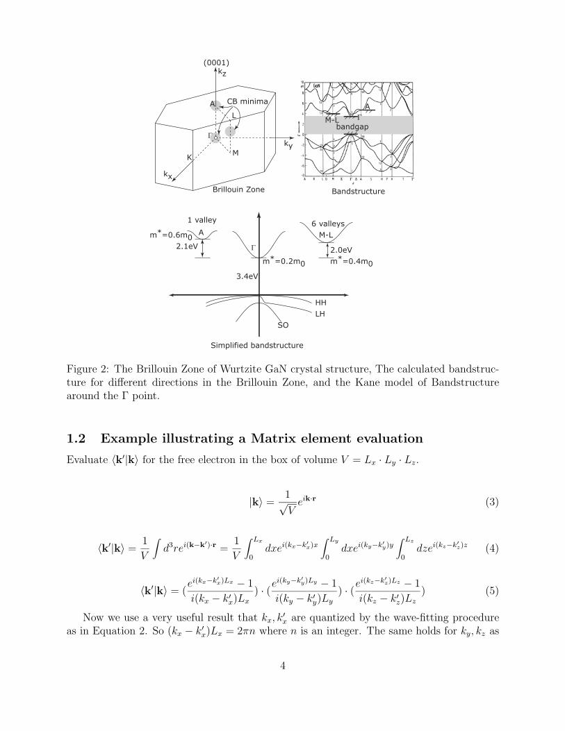
potential variation is periodic in nature. How is this problem solved? Bloch’s theoremprovides the vital link to the solution of the problem. It turns out that in a perfect crystal,you can remove the whole periodic crystal potential and lump it into the wonderful conceptof the ‘effective mass’ of the electron. By doing so, you have freed the electron from theshackles of widely fluctuating Coulombic potentials and have reduced the problem to thatof an electron in free space, albeit with a different mass 1. Solving the problem for theelectron taking the periodicity of the crystal into account yields the bandstructure of thesemiconductor, which stores a wealth of information. The Brillouin Zone, the bandstructure,and the simplified bandstructure around the CB minima and VB maxima for GaN, whichis the region of interest for most problems is shown in Figure 2. It is important to notethat the bandstructure is nothing but the allowed eigenvalues of the quantum mechanicalproblem for the perfect semiconductor. The k-values are quantized; the quantization is sofine that for all practical purposes, it is assumed continuous.
We now direct our attention towards the problem at hand - how to understand transporttheory. So the model we start with is really the first problem of an undergraduate quantummechanics class - you have a particle (electron, effective mass m∗) in a macroscopic crystal(say a GaN crystal). Let us assume the shape of the crystal to be a cube of side L 2. Sincethe particle is confined in a box, we model it as an infinite quantum well in 3 dimensions. Itis the good old particle in a box problem, which has well known solutions. The wavefunctionof the electron will be
ψ(x, y, z) =1√L3ei(kxx+kyy+kzz) =
1√L3eik·r (1)
which when subjected to the boundary conditions 3 yields the limits on the wavevectors-
k = (kx, ky, kz) =2π
L(nx, ny, nz) (2)
where nx, ny, nz are allowed only integral values (...,-1,0,1,...). The energy is E(k) = h2|k|22m∗
and the momentum is p = hk. The wavevector k for a free electron (not in a box) is relatedto its wavelength by the de Broglie relation λ = h
p; it is easy to see that it translates to k = 2π
λ.
When the electron is confined in a box, it can have only those wavelengths that can fit in thebox; so, the wavelengths are ‘quantized’, according to k. Electrons with wavevectors k → 0have very small momentum and are delocalised over the whole crystal, since their λ → ∞.On the other hand, electrons with large wavevectors have really small wavelengths, and canbe fitted into small microscopic areas. We will see how this is crucial in the phenomenonof screening, a very important phenomenon in transport and indeed in all of semiconductorphysics.
1This is the reason why you see that effective mass is not a scalar, but has dependence on the wavevectork. Roughly, since all directions are not the same in a crystal, neither should the periodic potential (andhence the effective mass in that direction). For our purpose though, we will be happy to deal with a directgap semiconductor that has an isotropic effective mass at the Γ point of the conduction band.
2L can be 1 cm; it is a macroscopic length, not microscopic!3The periodic boundary condition requires ψ(x+ L, y, z) = ψ(x, y + L, z) = ψ(x, y, z + L) = ψ(x, y, z)
3
Γ
K
A
ky
kz
kx
M
L
(0001)
ΓA
M-Lbandgap
Γ
M-LA
HHLH
SO
3.4eV
2.1eV 2.0eV
1 valley 6 valleys
m*=0.4m0
m*=0.6m0
m*=0.2m0
CB minima
Brillouin Zone Bandstructure
Simplified bandstructure
Figure 2: The Brillouin Zone of Wurtzite GaN crystal structure, The calculated bandstruc-ture for different directions in the Brillouin Zone, and the Kane model of Bandstructurearound the Γ point.
1.2 Example illustrating a Matrix element evaluation
Evaluate 〈k′|k〉 for the free electron in the box of volume V = Lx · Ly · Lz.
|k〉 =1√Veik·r (3)
〈k′|k〉 =1
V
∫d3rei(k−k′)·r =
1
V
∫ Lx
0dxei(kx−k′
x)x∫ Ly
0dxei(ky−k′
y)y∫ Lz
0dzei(kz−k′
z)z (4)
〈k′|k〉 = (ei(kx−k′
x)Lx − 1
i(kx − k′x)Lx
) · (ei(ky−k′
y)Ly − 1
i(ky − k′y)Ly
) · (ei(kz−k′
z)Lz − 1
i(kz − k′z)Lz
) (5)
Now we use a very useful result that kx, k′x are quantized by the wave-fitting procedure
as in Equation 2. So (kx − k′x)Lx = 2πn where n is an integer. The same holds for ky, kz as
4

well. Using this, we see that unless kx = k′x, ky = k′y, kz = k′z all hold true, the value of theintegral would be zero. If they do hold, the value is ONE (prove it!). Thus, the result is
〈k′|k〉 = δkx,k′xδky ,k′
yδkz ,k′
z= δk,k′ (6)
2 Transport of Bloch electrons in perfect semiconduc-
tors
Consider a semiconductor crystal that is perfect - i.e., there are no defects or impurity dopingof any kind. Let us follow the motion of an electron in the valence band in the presenceof a force (due to electric field), pointing to the right (+k) (see Figure 3). A force impartsmomentum to the electron, moving it into the next nearest state on the right, the electronin the next nearest state to its nearest state on right, and so on, according to the ‘Newton’slaw’ in k-space,
F = hdk
dt. (7)
The force may be due to an externally applied electric field (E), magnetic field B, or acombination of both. In general, one writes the equation of motion as
F = (−e) · [E + v × B] = hdk
dt. (8)
The electron at the end of the Brillouin Zone (BZ) in the VB “flips over”, and re-entersthe 1st BZ from the left, by acquiring a reciprocal lattice vector G from the lattice; such aprocess is called an Umklapp4 process. Umklapp processes occur so long as the field is nottoo high to cause the transition of an electron from one band to the other. If the force is toostrong, instead of Umklapp processes, an electron can ‘tunnel’ through the forbidden gap tothe next nearest empty band - this is the famous ’Zener’ tunneling process, which is usedfor commercially available Zener diodes.
The role of the force (through the electric field) is to impart the electron momentum;the velocity and acceleration of the electrons are determined by the bandstructure. We haveseen already that the velocity is given by
v =1
h
∂E(k)
∂k=
1
h∇kE(k), (9)
and the acceleration is given by
a =F
m. (10)
Keeping these facts in mind, we plot the bandstructure, the effective mass m, the ve-locity, and the acceleration of the electron in the valence band in Figure 3.
Many important features can be inferred from this figure. First, if one has a valence bandfilled with electrons, there can be NO NET CURRENT in a perfect semiconductor, even in
4The German verb umklappen means to flip over.
5

-G/2 G/2
E E
k
k
a a
v v
m* m*
0
Bandstr
uctu
reEffective
m
ass
Velo
city
Accele
ration
ValenceBand
ConductionBand
Figure 3: Bandstructure, effective mass, velocity, and acceleration of Bloch electrons in avalence and a conduction band.
the presence of an electric field. This happens since the electrons move within the bands inendless cycles, and a sum of the velocities due to all electrons is zero, since for every electronwith a positive velocity, there is one with an equivalent negative velocity.
Strange things happen if one considers only ONE electron moving in a empty conductionband in a perfect semiconductor crystal. From Figure 3, it is clear that similar to the motionof an electron in the filled valence band, the electron in the CB will undergo oscillations ink-space, as well as real space. This is because after each cycle of period T = hG/F , theelectron returns to where it started from in both k-space (obvious), and in real space as well(since area under velocity -time curve is zero)! Such oscillations are called Bloch oscillations,and they remain a source of great interest to this day, as a possible source of microwaveradiation.
However, we know very well that in real semiconductors, when one applies a force oncarriers (via electric field), there is a current. The reason is the presence of scattering. Inreal semiconductors, there will always be impurities present, which will scatter carriers, andBloch oscillations are stopped far before carriers can reach the edge of the Brillouin zones.Carrier scattering forces electrons back to the bottom of the CB or holes back to top of theVB; thus, we can conclude that characteristic scattering times (such as those that enter inthe expression for mobility, µ = eτ/m) are far smaller that the Bloch oscillation period.
6

This leads us naturally to study transport in real semiconductors, which is dominated byscattering off impurities, defects, and phonons, all of which are perturbations from the perfectcrystal.
3 Effective Mass Approximation, Envelope Functions
Before we jump into considering real semiconductors with impurities and correspondingperturbations from perfect periodic potentials, it is worthwhile to develop a very powerfulformalism that greatly simplifies our treatment of transport properties. So long as theperturbations of the crystal potential is not drastic, one can re-cast the Schrodinger equationin a form that is very useful for discussing transport and device applications. One runs intoa fundamental problem in dealing with a particle location in real space and its momentumat the same time. To do that, the concept of a wave packet is necessary. Wave packets,unlike pure Bloch-eigenstates, have a finite spread both in the momentum and real space.A wave packet is nothing but a linear combination of Bloch eigenstates for small k−valuesaround a region of interest in the Brillouin zone. For most cases, it suffices to investigateproperties of electrons and holes located very close to the band extrema in the k−space;therefore, one collects Bloch eigenstates around such points, and creates a wavepacket bytaking their linear combinations.
To illustrate this, let us consider the 1-dimensional case. We construct a wavepacket bytaking a linear combination of Bloch eigenstates φnk(x) from the nth band with wavevectork. The sum is over the whole BZ.
ψ(x) =∑n
∑k
C(k)φnk(x) =∑n
∫ dk
2πC(k)φnk(x) (11)
We now make two crucial approximation -a) We assume that wavefunctions from only one band play a part in the wavepacket, andthus drop the sum over all bands.b) We assume that in the single band we are interested in, wavevectors from a small regionsay around k0 = 0 are important (see Figure 4).
Then, Bloch functions can be written as φnk(x) = eikxunk(x) ≈ un0(x)eikx = φn0(x)e
ikx.Then the wavepacket takes the form
ψ(x) ≈ φn0(x)∫ dk
2πC(k)eikx = φn0︸︷︷︸
Bloch
· C(x)︸ ︷︷ ︸envelope
, (12)
where the integral term is identified as the Fourier transform of the weights C(k) ↔ C(x).The real-space function C(x) which is a Fourier transform of the weights of the wavepacket iscalled as the envelope function; since the weights C(k) are over a small region in k−space,C(x) is spread over real space. It is typically a smooth function spreading over several latticeconstants. This is illustrated in Figure 5.
How does the wavepacket behave when we apply the periodic crystal Hamiltonian H0
on it? Since φnk(x) are Bloch-eigenfunctions of this Hamiltonian, H0φnk(x) = En(k)φnk(x),
7

E
kk0
∆k ∆r∼1/∆k
atomsr
RECIPROCAL
SPACE
REAL
SPACE
ψπ
φ
ψ
( )( )
( ) ( )
( ) ( )
( )
rd k
C k r
r C r
d
d nk
k k k
envelopefunctio
=
→ ≈
∈ ±∆∫ 20
nn
nk
BlochFunction
r
φ0( )
π/a−π/a
Figure 4: A wavepacket is constructed by taking Bloch functions from a small region of thereciprocal space, and summing them with weights. The weights C(k) have a small extent ∆kin reciprocal space; when carried over to real space, the spread is large, since ∆r ∼ 1/∆k;thus the wavepacket has a finite spread in real space, and represents the wavefunction of aparticle. If we restrict the sum in reciprocal space to 1% of the BZ, the wavepacket spreadsover 1/0.01 = 100 atoms in real space. The real space wavefunction is given by the Blochwavefunction at the k0 point, modulated by an envelope function C(r), which is the Fouriertransform of the weights C(k).
and we recover
H0ψ(x) =∫ dk
2πC(k)En(k)φnk(x) ≈ φn0(x)
∫ dk
2πC(k)En(k)eikx. (13)
We now write out the energy eigenvalues as a Taylor-series of small wavevectors aroundk = k0 = 0,
En(k) =∑m
amkm (14)
and Schrodinger equation becomes
Hψ(x) ≈ φn0(x)∑m
∫ dk
2πC(k)kmeikx. (15)
We now use a property of Fourier transforms - if f(k) ↔ f(k), then kf(k) ↔ (−id/dx)f(x),and in general, kmf(k) ↔ (−id/dx)mf(x). Thus,
∫ dk
2πkmC(k)eikx ↔ (−i d
dx)mC(x), (16)
and the Schrodinger equation is recast as
8

Periodic Part ofBloch Functions
EnvelopeFunction
Atoms
φni r
n nr e u r u r0
0
0 0( ) ( ) ( )( )= =⋅
C r( )
ψ φ( ) ( ) ( )r r C rn≈ 0
Envelope Function
Figure 5: Envelope function C(r) modulates the Bloch function φn0(x) to produce the wave-function of the wavepacket ψ(x)
Hψ(x) ≈ φn0(x)En(−i∇)C(x), (17)
which can be generalized to the 3-D case. Thus, in the energy term, we make the substitutionk → i∂/∂r, making it an operator that acts on the envelope function only. This step is crucial- the Bloch function part has been pulled out as a coefficient; no operators act on it.
Now, instead of the periodic potential Hamiltonian, if we have another potential (say aperturbation) V (r) present, Schrodinger equation becomes
H0φn0(r)C(r) + V (r)φn0(r)C(r) = Eφn0(r)C(r), (18)
and using Equation 17, it becomes
[En(−i∇) + V (r)]C(r) = EC(r), (19)
where the Bloch functions do not appear at all! Furthermore, if we already know thebandstructure of the semiconductor, then we can write the energy around the point k0 = 0of interest in terms of the effective mass, and the operator En(−i∇) thus becomes
En(k) ≈ Ec(r) +h2k2
2m→ En(−i∇) ≈ Ec(r) − h2
2m∇2, (20)
and the Schrodinger equation takes the enormously simplified form
[− h2
2m∇2 + Vimp(r)]C(r) = [E − Ec(r)]C(r), (21)
which is the celebrated “Effective Mass Approximation”. Take a moment to note whathas been achieved. The Schrodinger equation has been re-cast into a much simpler prob-lem of a particle of mass m, moving in a potential Ec(r) + V (r)! All information aboutthe bandstructure and crystal potential has been lumped into the effective mass m. Thewavefunctions are envelope functions C(r), from which one recovers the real wavefunction of
9

the wavepacket by multiplying with the Bloch function - ψ(r) ≈ φn0(r)C(r) = un0(r)C(r).The envelope functions C(r) can be actually determined for any potential - it amounts tosolving the Schrodinger equation for a particle in the potential Ec(r) + V (r). Note that theenvelope function in the absence of any impurity potential V (r) = 0 is given by
C(r) =1√Veik·r, (22)
and the corresponding eigenvalues of the Schroodinger equation are given by
E = Ec(r) +h2|k|22m
. (23)
If we consider electrons at the bottom of the conduction band, Ec(r) is the spatial varia-tion of the conduction band edge - exactly what one draws in band diagrams. An impuritypotential can now be included as a perturbation to the periodic crystal, and the new energyeigenvalues can be found. As an example, consider an ionized impurity, which has a Coulombpotential. The effective mass equation takes the form
[− h2
2m∇2 − e2
4πεr]C(r) = (E − Ec)C(r), (24)
which is identified as the same as the classic problem of a hydrogen atom, albeit with twomodifications - the mass term is an effective mass instead of the free electron mass, and thedielectric constant is that of the semiconductor. Then, the new energy levels that appearare given by
E − Ec = E∞m
ε2r, (25)
and the effective Bohr-radius is given by
aB = aB
εrm
(26)
In bulk semiconductors, the band-edge variation in real space can be varied by applyingelectric fields, or by doping variations. In semiconductor heterostructures, one can furtherengineer the variation of the band-edge Ec(r) in space by quasi-electric fields - the band edgecan behave as quantum-wells, wires, or dots, depending upon composition of the semicon-ductor. The effective mass approximation is a natural point of departure, where analysis ofsuch low-dimensional structures begins.
4 Transport theory - Real Semiconductors
If you apply an electric field and measure the drift velocity of electrons in a bulk semicon-ductor, you will see what is called the velocity-field characteristic. It is schematically shownin the left part of Figure 6. Drift velocity is proportional to the applied field for low fields;this is the ‘ohmic’ regime characterized by the electron mobility µ = vd/F . As you rampup the field, the velocity will approach a saturation value - this is the ‘hot-electron’ regime
10

of transport. If you run Hall measurements on mobile carriers in a bulk semiconductor anda two-dimensional electron gas at varying temperatures and measure the mobility, you willsee behavior depicted in the right part of Figure 6. Most of our study in transport theoryis geared towards understanding from a quantum-mechanical viewpoint the reasons for thiskind of behavior.
vd
F
vcmssat ∼ 107
µ( )300 10002
KvF
cmV s
d=⋅
∼
overshoot
T
µ
2DEG
Bulk
Si
GaAs
Figure 6: Velocity field curves (left) of Si and GaAs showing some definitions. Mobility versustemperature for generic semiconductor bulk and two-dimensional electron gas (2DEG). Thefigure is for motivating the study of transport theory
4.1 Setting up the Quantum Mechanical Problem
We begin with a completely general time-dependent Schrodinger equation
ih∂
∂tΨ(r, t) = (H0 +H1)Ψ(r, t) (27)
We split the Hamiltonian into two parts. The first part,
H0 = − h2
2m∇2 + EC(r) (28)
is the Effective Mass Hamiltonian that we derived earlier (Equation 21). For a bulksemiconductor, H0 is the crystal potential, which upon solution yields the bandstructure asthe eigenvalues. We then concentrate on only the small region around the band extrema(CB minima or VB maxima).
The second part of the Hamiltonian is a small perturbation to the CB minimum intro-duced by impurities such as charged dopants, vacancies, or dislocations -
H1 = Perturbation (29)
11

Solving the exact part gives us the set of eigenfunctions Φm(r) and eigenvalues Em cor-responding to the Hamiltonian of the pure system, H0 -
H0Φm(r) = EmΦm(r) (30)
For the time dependent solution of the problem (with the scattering potentials), weexpand the time dependent wavefunction in terms of the unperturbed eigenfunctions -
Ψ(r, t) =∑m
ψm(t)Φm(r) (31)
The time-dependent equation (Equation 27) then becomes
ihd
dtψm =
∑n
〈m|H|n〉ψn (32)
Since the H0 part has been solved exactly, we can use it to get the relation
d
dtψm(t) +
iEm
hψm =
∑n
〈m|H1|n〉ih
ψn (33)
For a homogenous semiconductor, the solutions of the pure Hamiltonian are planewaves
Φk(r) =1√Veik·r, (34)
where V = LxLyLz is the sample volume. The quantization of wavevectors is given byki = ni
2πLi, i = x, y, z. The corresponding eigenvalues are given by
Ek = EC +h2|k|22m
(35)
4.2 Fermi’s Golden Rule
Evaluation of scattering rates requires us to use one of the most useful results of timedependent perturbation theory in quantum mechanics. Don’t throw your hands up in despair,since it is not only simple, it is extremely useful too. Knowing it will help you figure out alot of stuff in your research, no matter which field you are thinking about working in. Theresult is known by the glorified name of ‘Fermi’s Golden Rule’5.
We will derive Fermi’s Golden Rule (FGR6) with the following problem in mind. Wehave an incident electron with wavevector along the z direction (Figure 7) in a uniformbulk semiconductor of dimensions V = LxLyLz. The semiconductor is pure, except for asmall impurity with a time-independent potential U(r) located somewhere in the bulk. Theincident beam wavefunction is given by eikz where k = |k|.
We have a detector at an angular position (θ, φ) and would like to find the probabilityPS(θ, φ) of finding the portion of the beam scattered by the potential U(r) at that angular
5Golden is no exaggeration; however, refer to Kroemer’s book, pg. for what he has to say about licensingthe rule!
6I hate acronyms myself when I come across them. Please bear with me for this one three letter word!
12

U(r)
k
k’
L z
L yL xA=
Detector
e ikz
x
yz
Figure 7: Figure for setting up the problem of scattering. An incident electron is scatteredby a scattering potential U(r) in an otherwise pure semiconductor. A detector is placed tofind the angular dependence of scattering.
location. The result we derive is valid only in a weak scattering limit, i.e., the total scatteringprobability is much less than unity
PS =∫ π
0dθ sin(θ)
∫ 2π
0dφP (θ, φ) 1 (36)
In Equation 33, we saw how the time-coefficients of the solved wavefunction are linkedto impurity potentials. A perturbation always causes transitions between allowed statesof a exactly solved problem with known eigenfunctions and eigenvalues. In this problem,the exactly solved problem is again of the semiconductor bandstructure with allowed statesindexed by the wavevectors |k〉. The eigenfunction and eigenvalues are given by Equation 34and Equation35 respectively.
To evaluate the probability of a state in the eigenstate |k〉 to scatter into any state |k′〉,we have to find the amplitude of that state in the eigenfunction expansion and square it.The amplitudes are governed by Equation 33. We now revert to the quantum number index(m,n) → (k, k′) since the allowed states have been solved. Starting with the equation
d
dtψk′(t) +
iEk′
hψk′ =
∑k′′ =k′
〈k′′|H1|k′〉ih
ψk′′ (37)
The electron is incident with a wavevector along z at t = 0. So, the initial wavefunctionis
13

Ψ(r, t = 0) =1√Veik·r (38)
From Equation 31, we get Ψ(r, t = 0) =∑
k′ ψk′(t = 0)Φk′(r). So ψk′(t = 0) = 1 fork′ = k and 0 for all other k′. To find the amplitudes ψk′(t) at all other times, we have tosolve Equation 33. If the scattering potential is absent (U(r) = 0), then the equation issolved easily, giving
ψ0k′(t) = ψ0
k′(0)e−iEk′ t
h . (39)
We label the solution by ‘0’ to emphasize that it is a zero order solution. From Equa-tion 31, it is easy to see that only the amplitude of state |k′〉 = |k〉 evolves with time,whereas the amplitude of all other states is 0. When there is a nonzero scattering potential,there are transitions between different eigenstates, so the amplitudes of |k′〉 = |k〉 will notbe zero anymore. However, the solution of Equation 33 is not simple anymore, and we haveto take the route of successive approximations now. It is crucial to understand this part toappreciate the limitations of FGR.
We start by substituting the solution of the zero order solution on the RHS of Equation 33and solve for the first order solution. This process is repeated for higher order solutions.However, if the scattering potential happens to be weak, it turns out that the first ordersolution is adequate and leads to Fermi’s Golden Rule. Doing that, our time evolutionequation becomes
d
dtψk′(t) +
iEk′
hψk′ =
〈k′|U(r)|k〉ih
e−iEk′ t
h (40)
Subject to the initial condition Equation 39, the solution gives the amplitude of state|k′〉 at time T
ψk′(T ) = e−iEk′T
h〈k′|U(r)|k〉
ih
∫ T
0e−i
(Ek−Ek′ )Th dt (41)
Thus, the probability of finding an electron scattered into the final state |k′〉 is the squareof the amplitude of that state. That is exactly what we have determined in Equation 41.So,
P (k′,k) = |ψk′(T )|2 =|〈k′|U(r)|k〉|2
h2 |∫ T
0e−i
(Ek−Ek′ )Th dt|2 (42)
T can be seen as the time taken for the electron to traverse the length Lz; it is thus givenby T = Lz
v= mV
hkA, where A = LxLy is the cross sectional area. The probability can be recast
in the form
P (k′,k) = T|〈k′|U(r)|k〉|2
h2 g(Ek′ − Ek) (43)
where
g(ε) =1
T|sin(εT/2h)
(εT/2h)|2 (44)
14

Using a special property of the function∫+∞−∞ dεg(ε) = 2πh, we see that in the limit of a
long time T → ∞, the function g becomes a delta function. Thus, LimT→∞g(ε) = 2πhδ(ε).This allows us to write the probability as
P (k′,k) = TS(k′,k) (45)
where
S(k′,k) =2π
h|〈k′|U(r)|k〉|2δ(Ek′ − Ek) (46)
This is the traditional way of stating the famous FGR for time-independent stationarypotentials. Note that this is not yet a measurable probability, since the measured probabilitywill be a sum over all |k′〉 states. Thus, to find a measurable probability, we need to sumthe probability over all such final states.
PS =∑k′P (k′,k) (47)
Using the recipe∑
k′(...) → V(2π)3
∫d3k′(...), we get
PS =V
(2π)3
∫ ∞
0
∫ π
0
∫ 2π
0k′2dk′ sin(θ)dθdφP (k′,k) (48)
Remembering the problem we started out with, we see that the angular probability cannow be evaluated. Comparing with Equation 36, we write
P (θ, φ) =V
(2π)3
∫ ∞
0dk′k′2P (k′,k) (49)
Using FGR for P (k′,k), we get
P (θ, φ) =V T
4π2h
∫dk′k′2|〈k′|U(r)|k〉|2δ(Ek′ − Ek) (50)
We now use two important techniques. We transform the variable of integration to theargument of the delta function (k′ → Ek′) using the identity dk′ = dk′
dEk′dEk′ = mk′
h2 dEk′ . We
do this to take advantage of a very important property of a delta function -
∫ b
adεδ(ε− ε0)F (ε) = F (ε0) (51)
if a < ε0 < b, and is 0 otherwise. Using this useful result, we get
P (θ, φ) =V T
4π2h
mk
h2 |〈k′|U(r)|k〉|2 (52)
The delta function enforced energy conservation in the scattering process (Ek′ = Ek),and as a result, also required us to conserve the magnitude of momentum (k′ = k). Usingthe explicit form of the matrix element 〈k′|U(r)|k〉 = 1
V
∫d3U(r)ei(k′−k)·r, we write the
probability in the form
15

P (θ, φ) =(m)2
4π2h4A|∫d3U(r)ei(k′−k)·r|2 (53)
The angular dependence is hidden in the (k′ − k) term. We will encounter it whenstudying ionized impurity scattering that has a strong angular dependence.
This result can be recast in a visually more appealing form by rewriting P (θ, φ) asP (θ, φ) = σ(θ, φ)/A, where
σ(θ, φ) =(m)2
4π2h4 |∫d3U(r)ei(k′−k)·r|2 (54)
is referred to as the ‘scattering cross section’. The total scattering scattering cross sectionσS is evaluated by integrating over all angular contributions
σS = PSA =∫ π
0dθ sin(θ)
∫ 2π
0dφσ(θ, φ) (55)
Scattering cross section lets us visualize the scatterer as a solid obstacle of cross sectionalarea σS, which will scatter an electron with the probability σS/A. The typical problem intransport is electrons moving in a semiconductor with a density NI of scattering centers (orimpurities. In time t, the total number of scatterers an electron encounters will be NIAvtwhere v is the velocity. Thus, the probability that the electron will be scattered in time t is
Pr(t) =t
τ=
t1
σSNIv
(56)
This relation holds only for short intervals (t τ). For large t, it is Pr(t) = 1 − e−tτ
(prove it!). Thus using T = Lz
v= mV
hkA, P (k′,k) = TS(k′,k), and PS =
∑k′ P (k′,k), the
mean free time between two scattering events (collisions) can be written as
1
τc= σSvNI =
∑k′
(NIV )S(k,k′) (57)
This relation is easy to understand.∑
k′ S(k,k′) is the rate at which an electron ofmomentum k is scattered by a single impurity. Multiplying by the total number of impuritiesNIV , the total scattering rate is obtained.
To find the scattering time that goes into determining mobility, we have to use themomentum scattering rate, τm. Experimental mobility is related to the momentum scatteringtime by µ = eτm/m
. The scattering rate we just derived is the inter-collision time. Collisionrate is 1
τQwhere τQ, the collision time determined by FGR is also called the quantum lifetime.
From Figure 8, we note that some scattering events can change the angle of the k vector byvery large amounts. Others have a weak effect. If there is small angle scattering, the currentis higher, and hence the mobility is higher, so the momentum scattering rate is smaller. Ifthe angle of scattering is large, momentum scattering rate will be smaller than the quantumscattering rate. This can be heuristically built into the formalism by writing
1
τm=
1
τQ[1 − cos(θ)] =
1
τQ[1 − k0 · k1
|k0|2 ] (58)
16

k0
k1
θ
θ
1 11
τ τθ
m Q
Cos= −[ ( )]
F
k1
Figure 8: Figure to show the difference between the quantum lifetime τQ and the transportlifetime τm. If there is a small angle scattering, current is higher, and thus mobility is higher.For large angle scattering, current is lower, and mobility is lower. Thus, heuristically, we cansay that the momentum lifetime and quantum lifetime (which is time between collisions) arerelated by 1
τm= 1
τQ(1 − cos(θ))
This result can be got by a rigorous analysis, so we believe in it and go ahead and use itto calculate mobility. Thus, momentum scattering rate is given by incorporating this smallchange to Equation 37 -
1
τc= σSvNI =
∑k′
(NIV )S(k,k′)(1 − cos(θ)) (59)
where cos(θ) = k·k′|k|2 .
4.3 Example illustrating application of Fermi’s Golden Rule
To get comfortable with Fermi’s Golden rule we apply it to study scattering of a wavelikeparticle from a rectangular barrier of height and thickness d.
Consider the problem of a wave incident on the rectangular barrier. The classical prob-ability of reflection R is 1 for energy E < and 0 for E > . Quantum mechanically, thebehavior is more interesting. The reflection probability is given by
R =2R− 2R cos(2k1d)
1 +R2 − 2R cos(2k2d)(60)
where R = |r|2 is the reflection probability for a single barrier, and r = k1−k0
k1+k0is the
reflection amplitude for a single barrier. Let us see how we can apply Fermi’s Golden Ruleto solve the same problem.
Fermi’s Golden Rule will tell us the probability of scattering due to a small perturbationto the exactly solved Hamiltonian potential. Here, the exactly solved Hamiltonian is the freeelectron Hamiltonian. The solved wavefunctions are planewave states, given by
|k〉 =1√Veik·r (61)
17

If the particle is reflected from the barrier, we say that it has been scattered. FGR willtell us the probability of this event -
PS = T∑k′S(k′, k) =
∑k′
2πT
h|U(k′,k)|2δ(Ek′ − Ek′) (62)
The barrier is in the z direction; the initial momentum vector of the electron points inthe z direction - kz = k0, kx = ky = 0. So the matrix element of the barrier potential is givenby
〈k′||k〉 =V
∫ Lx
0dxei(kx−k′
x)x∫ Ly
0dxei(ky−k′
y)y∫ d
0dzei(kz−k′
z)z (63)
which, on using results of Example 1 evaluates to
〈k′||k〉 =Lz
δkx,k′xδky ,k′
y(ei(kz−k′
z)d − 1
i(kz − k′z)) (64)
Thus, the scattered electrons have the same transverse momenta as the incident (kx, ky) =(k′x, k
′y). So, the sum over all scattered k′ runs over only k′z. Thus, we have
PS =∑k′
z
2πT
h|U(k′,k)|2δ(Ek′ − Ek′) (65)
where
|U(k′,k)|2 =42
L2z(k − k′z)2
sin2((k − k′z)d
2) (66)
Converting the sum over k′z to an integral using the recipe∑
k′z(...) → Lz
2π
∫dk′z(...) and
using the transformation dk′z = dEk′ dk′z
dEk′we get
PS =LzT
h
∫dEk′δ(Ek′ − Ek)
dk′zdEk′
|Uk,k′|2 (67)
The delta function forces energy conservation; k′ = k → k′z = k0. Also, dk′z
dEk′= m
h2k′z.
Using this, the scattering probability becomes
PS =mT2
h3k30Lz
sin2(k0d) (68)
Using T = Lz
v0= mLz
hk0, we get
PS = (m
h2k20
)2 sin2(k0d) (69)
This is the final scattering rate. It certainly does not look like the quantum mechanicalresult for probability of reflection as in Equation 38. The difference brings in focus theassumptions that are inherent in FGR. Consider the QM result. Let us see how the expressionlooks for small R. Then, neglecting R and R2 in the Dr, the expression for reflectionprobability Equation 38 reduces to
18

RB 2R− 2R cos(2k2d) = 4R sin2(k2d) =4(k2 − k1)
2
(k2 + k1)2sin2(k2d) (70)
If R is small, k2 k1 = k0, and the expression becomes
RB (k2 − k1
k0
)2 sin2(k0d) (71)
Since k2 =√
2m∗(E−EC−)
h2 and k2 =√
2m∗(E−EC)
h2 , k22 − k2
1 = 2mh2 2k0(k2 − k1). Using
this, the result becomes
RB (m
h2k20
)2 sin2(k0d) (72)
This is exactly the result we got from the FGR calculation. So the assumption in FGRof a weak scattering potential is very important and should always be borne in mind whenapplying the rule.
FGR has widespread customers. A short list of it’s clients other than semiconductortransport are optics, atomic processes, spectroscopy (Raman, NMR, etc) etc. Whereverthere is a time-dependent transition between quantum mechanical states is involved, FGRrules.
5 Case study of scattering in semiconductors
Low field mobility is calculated by doing the following -
1) Identify the defect (perturbation) and choose a suitable model for it’s potential Ui(r)for the ith type of impurity.
2) Calculate the momentum scattering rate for the particular type of impurity and sumit over all available final states k′.
3) Calculate the total scattering rate using the Matheissen’s rule - 1τ
=∑
i1τi
.
4) Average the momentum scattering rate for drift velocity (Eqn 74).
5) Calculate the mobility using µ = eτm/m.
We have gone through the whole formalism and have armed ourselves now with all thetools needed for doing the above steps. The following sections would be really short sincewe have done all the hard work earlier.
19

5.1 Example - Ionized impurity scattering in bulk semiconductorsand 2DEGs
Consider an ionized impurity in a bulk semiconductor. We find the quantum scatteringtime τQ for scattering from state |k〉 to a general final state |k′〉. The impurity may be anintentional donor or acceptor, or a charged vacancy state or any such impurity. Let thecharge on the impurity be Z Coulombs. Equation 34, Equation 67 yield
σ(θ, φ) =4L4
D
a20
1
(1 + qLD)2(73)
where a0 = 4πε0Kh2
mq2 , the effective Bohr radius. Since Coulombic scattering is elastic,q = k − k′ can be written as
q2 = 2k2[1 − cos(θ)] (74)
where k = |k| = |k′|. Using this, writing γ = 2kLD and integrating over all angles (θ, φ)7,we get the total scattering cross section as
σS =π
k4a20
γ4
1 + γ2(75)
Thus, from Eq. 37, the quantum scattering rate is given by
1
τQ(k)= NI · hk
m· π
k4a20
γ4
1 + γ2(76)
The momentum relaxation rate can be got similarly by using Equation 39. The result is
1
τm(k)= NI · hk
m· 2π
k4a20
[ln(1 + γ2) − γ2
1 + γ2] (77)
The total momentum scattering time is found by an averaging procedure. It is easy toconvert τm(k) → τm(E), since the dispersion E(k) = h2k2
2m is known. For drift velocity alongan applied field Fz (along the z axis), the averaging8 procedure for a Fermi-Dirac distributedcarrier population is given by
〈τm〉 = −2
3
∫ ∞
0
τm(E) ∂f0
∂(E/kBT )(E/kBT )3/2d(E/kBT )∫∞
0 f0(E/kBT )1/2d(E/kBT )(78)
Using this recipe, we get the mobility as
µimp =e〈τm〉m
=27/2(4πε0K)2(kBT )3/2
π3/2Z2e3(m)1/2NI [ln(1 + γ20) − γ2
0
1+γ20]
(79)
where Z is the total electron charges in the impurity and γ0 = 2m
h( 2
m 3kBT )1/2LD. Thedependence of this mobility on temperature T and impurity density NI is seen to be
7From now on, you need to evaluate all integrals yourself and verify the results!8Seeger, Semiconductor Physics, Pg 50
20

µimp ∝ T32
NI
(80)
In bulk semiconductors at low temperatures, ionized impurities set the mobility limits.This is the mobility dependence in Figure 4 at low temperatures (right curve, increasingmobility).
For 2DEGs, the phenomena of quantization and degeneracy of conducting electrons (allconducting electrons have k kF =
√2πn2D) change the averaging procedure9 and make
the problem easy. Also, the remote location of impurities (modulation doping) introducesan exponential decay of the Coulomb potential. This results in much higher mobilities. Animportant fact is there is no temperature activation of carriers required for a 2DEG; the2DEG density is independent of temperature. Thus, the ionized impurity limited mobilityis independent of temperature for a 2DEG. This results in the ‘flat’ mobility saturation atlow temperatures for 2DEGs (right plot, Figure 3).
5.2 Other scattering mechanisms and where to read about them
At room temperature, the mobility in a reasonably pure semiconductor is almost always lim-ited by phonon scattering. Phonon scattering is very important for operational devices andis treated well in Seeger’s book (Semiconductor Physics). In fact, all scattering mechanismsare very well treated in this book. I highly recommend it if you want to learn more on trans-port and scattering. However, Seeger’s book is an ‘old’ book, it does not include quantumstructures like quantum wells, etc. For a newer treatment (though not as comprehensive asSeeger), John Davies’ book (Physics of low dimensional semiconductors) is recommended.Another book which does a good and compact treatment of transport properties is Wolfe,Holonyak and Stillman’s ‘Physical properties of semiconductors’. For a comprehensive re-view of 2DEG transport properties, and every conceivable property of the 2DEG, refer tothe ‘Bible’ of 2DEGs - a journal article that can be downloaded from the web. The article isby Ando, Fowler and Stern; it appeared in Reviews of Modern Physics, (Rev. Mod. Phys.54, 437-672 (1982)).
Alloy disorder scattering is important for transport in ternary (or even binary - SiGe)alloys. For 2DEGs, interface roughness scattering becomes severe at high 2DEG densities.Dislocation scattering is proving to be a hindrance for the III-V nitride semiconductorsmaking it bigger than what they already are.
5.3 High field transport
Consider an electron moving in the presence of impurity scattering with an increasing electricfield. In the ‘ohmic’ regime we defined a mobility as the ratio of drift velocity and field. Nowin the microscopic picture, the electron starts from zero velocity, accelerates by gaining energyfrom the field, and then scatters. This is the way it traverses the length of a semciconductordevice. It is depicted in Figure 9.
9John Davies, Pg 356
21

After every scattering event, the electron starts gaining momentum (and hence energy)from the applied field. The energy it acquires before the next collision increases as theelectric field increases. At a particular value of the electric field, the energy gained betweentwo collisions becomes larger than the optical phonon energy hωop. When this happens, theprobability of the electron losing all it’s energy to the lattice by the emission of an opticalphonon becomes large. The emission of a phonon results in no increase in current; it justheats the device. Any further increase of the field will cause an increase in the number ofoptical phonons emitted, with no increase in the drift velocity. The drift velocity is said tobe saturated.
Device
Leftcontact
Rightcontact
0 Lz
kz
t
0
L
t
z(t)
Figure 9: Figure depicting the actual transport process with time. The second shows howthe z component of momentum increases linearly with time (kz(t) = F
ht) till it gets scattered
to a random state. The third figure shows the progress of the particle in real space withtime as it traverses the length of the device.
Thus, a fair back of the envelope estimate of the saturated drift velocity can be madeby equating the kinetic energy at the saturated drift velocity KE = 1
2mv2
d to the opticalphonon energy in the semiconductor -
vsatd ∼
√2hωop
3m(81)
For GaN, hωop = 92meV,m = 0.2m0, and the drift velocity estimate is vsatd ∼ 4 ×
107cm/s. This is a good ‘order of magnitude’ estimate. The true value is vsatd ∼ 2×107cm/s.
Thus, the velocity-field curve saturates; this is shown in Figure 3, left graph.In direct gap semiconductors (GaAs, GaN, etc) there are two CB minimum in the E − k
diagram. Γ valley is the lowest and X valley is the second lowest valley. The X valley has asmaller curvature and hence a larger effective mass. At high fields, when high ks are achieved
22

between collisions, it becomes possible for electrons to transfer from the Γ tot eh X valley;the onset of this phenomena causes a region where the velocity decreases with increasingfield. This is the origin of negative differential resistance (NDR) which is put to use to makeGunn oscillators which have very high frequency oscillations.
The velocity-field characteristics are of utmost importance in submicron devices. Thereason is that for the same applied voltage, the field in a small length device will be large.Thus, saturation of drift velocity is achieved under fairly low voltages. With the miniatur-ization of transistors and decreasing gate lengths, it is very important for a device engineerto understand the hidden theories behind the velocity-field characteristics for innovation.
5.4 Transport Regimes
In a sufficiently pure semiconductors, electron wavelengths are sufficiently delocalized andcan spread over large distances (large λ → small k). For such cases, transport occurs inthe bands, this regime of transport is called band transport. Figure 10 shows schematicallythis form of transport. For low field regime, the transport proceeds by scattering fromimpurities. For high field regime, there are optical phonon emissions, but all transport isin the conduction (or valence) band. If there is a lot of disorder in a semiconductor (say
Localizedcarrierpockets
F
Hoppingtransport
No carriers
F
Very large disorder (grains)
Carriers everywhere
Momentumdephasing byscattering
Dilute defects
k
Band transport
Low disorder (extended states)
Figure 10: Band transport and Hopping regimes of transport. Band transport has beendiscussed in this work. Hopping transport requires activation to surmount the barriersbetween nearby localized pockets of carriers.
an polycrystalline semiconductor with grain boundaries), then there will be small localizedpockets of carriers which will have to surmount the potential barriers between them tocarry current. This process requires an activation energy, and the activation energy can bemeasured. This form of transport is very different in characteristic from band transport.The transport is called ‘activated’ or ‘hopping’ transport because the carriers hop from one
23

localized state to the other. Theoretical treatment of transport in such disordered systemsrequires percolation theory and sophisticated techniques such as Green’s functions, which Ileave for you to explore.
6 Formal Transport theory
Much of the following summary is collected from textbooks and research articles. The mainreferences for this section are Seeger [1], Wolfe et. al. [2], and Davies [3]. No claim tooriginality is made for much of the material. The subsection on generalization of mobilityexpressions for arbitrary dimensions and arbitrary degeneracy is original, though much of itis inspired from the references.
6.1 Boltzmann transport equation
A distribution-function f(k, r, t) is the probability of occupation of an electron at time t atr with wavevectors lying between k,k + dk. Under equilibrium (E = B = ∇rf = ∇Tf = 0,i.e., no external electric (E) or magnetic (B) field and no spatial and thermal gradients), thedistribution function is found from quantum-statistical analysis to be given by the Fermi-Dirac function for fermions -
f0(ε) =1
1 + eεk−µ
kBT
, (82)
where εk is the energy of the electron, µ is the Fermi energy, and kB is the Boltzmannconstant.
Any external perturbation drives the distribution function away from the equilibrium;the Boltzmann-transport equation (BTE) governs the shift of the distribution function fromequilibrium. It may be written formally as [2]
df
dt=
Ft
h· ∇kf(k) + v · ∇rf (k) +
∂f
∂t, (83)
where on the right hand side, the first term reflects the change in distribution functiondue to the total field force Ft = E+v×B, the second term is the change due to concentrationgradients, and the last term is the local change in the distribution function. Since the totalnumber of carriers in the crystal is constant, the total rate of change of the distribution isidentically zero by Liouville’s theorem. Hence the local change in the distribution functionis written as
∂f
∂t=∂f
∂t|coll − Ft
h· ∇kf(k) − v · ∇rf(k) +
∂f
∂t, (84)
where the first term has been split off from the field term since collision effects are noteasily described by fields. The second term is due to applied field only and the third is dueto concentration gradients.
Denoting the scattering rate from state k → k′ as S(k,k′), the collision term is given by
24
∂f(k)
∂t|coll =
∑k′
[S(k′,k)f(k′)[1 − f(k)] − S(k,k′)f(k)[1 − f(k′)]]. (85)
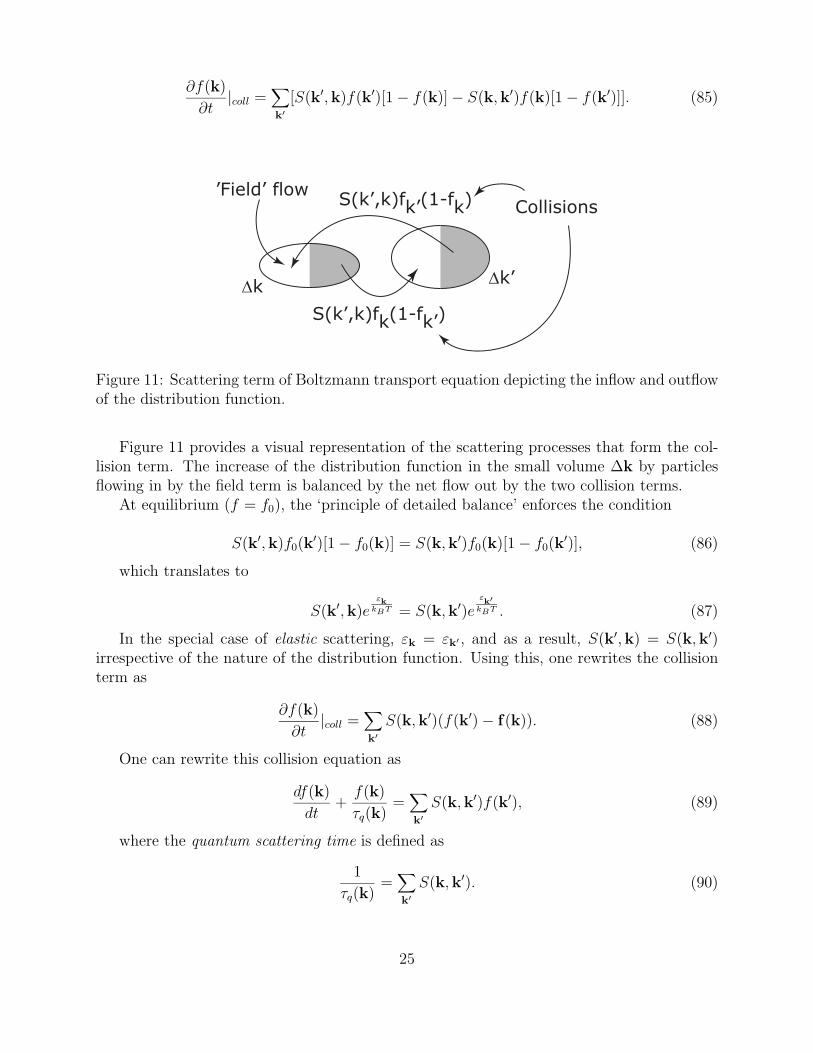
S(k’,k)fk’(1-fk)
S(k’,k)fk(1-fk’)
∆k’∆k
’Field’ flowCollisions
Figure 11: Scattering term of Boltzmann transport equation depicting the inflow and outflowof the distribution function.
Figure 11 provides a visual representation of the scattering processes that form the col-lision term. The increase of the distribution function in the small volume ∆k by particlesflowing in by the field term is balanced by the net flow out by the two collision terms.
At equilibrium (f = f0), the ‘principle of detailed balance’ enforces the condition
S(k′,k)f0(k′)[1 − f0(k)] = S(k,k′)f0(k)[1 − f0(k
′)], (86)
which translates to
S(k′,k)eεk
kBT = S(k,k′)eεk′
kBT . (87)
In the special case of elastic scattering, εk = εk′ , and as a result, S(k′,k) = S(k,k′)irrespective of the nature of the distribution function. Using this, one rewrites the collisionterm as
∂f(k)
∂t|coll =
∑k′S(k,k′)(f(k′) − f(k)). (88)
One can rewrite this collision equation as
df(k)
dt+f(k)
τq(k)=∑k′S(k,k′)f(k′), (89)
where the quantum scattering time is defined as
1
τq(k)=∑k′S(k,k′). (90)
25

A particle prepared in state |k〉 at time t = 0 by an external perturbation will be scat-tered into other states |k′〉 due to collisions, and the distribution function in that state willapproach the equilibrium distribution exponentially fast with the time constant τq(k) uponthe removal of the applied field. The quantum scattering time τq(k) may be viewed as a‘lifetime’ of the particle in the state |k〉.
Let us now assume that the external fields and gradients have been turned on for a longtime. They have driven the distribution function to a steady state value f from f0. Theperturbation is assumed to be small, i.e., distribution function is assumed not to deviate farfrom its equilibrium value of f0. Under this condition, it is common practice to assume that
∂f
∂t=∂f
∂t|coll = −f − f0
τ, (91)
where τ is a time scale characterizing the relaxation of the distribution. This is therelaxation time approximation, which is crucial for getting a solution of the Boltzmanntransport equation.
When the distribution function reaches a steady state, the Boltzmann transport equationmay be written as
∂f
∂t= −
(f − f0
τ
)− Ft
h· ∇kf(k) − v · ∇rf(k) = 0, (92)
where the relaxation time approximation to the collision term has been used. In theabsence of any concentration gradients, the distribution function is given by
f(k) = f0(k) − τFt
h· ∇kf. (93)
Using the definition of the velocity v = 1/h(∂εk/∂k), the distribution function becomes
f(k) = f0(k) − τFt · v∂f(k)
∂ε, (94)
and since the distribution function is assumed to be close to f0, we can make the replace-ment f(k) → f0(k), whence the distribution function
f(k) = f0(k) − τFt · v∂f0(k)
∂ε(95)
is the solution of BTE for a perturbing force Ft.
6.1.1 Electric field
The external force Ft may be due to electric or magnetic fields. We first look for the solutionin the presence of only the electric field; thus, Ft = −eE.
Using Equation 95, for elastic scattering processes one immediately obtains
f(k′) − f(k) = eτ∂f0
∂εE · v︸ ︷︷ ︸
f(k)−f0(k)
(1 − E · v′
E · v ) (96)
26

k
k’
E
θ
αβ
γ
z
x
y
Figure 12: Angular relations between the vectors in Boltzmann transport equation.
for a parabolic bandstructure (v = hk/m). Using this relation, the collision term in theform of the relaxation time approximation becomes
∂f(k)
∂t=∑k′S(k,k′)(f(k′) − f(k)) = −(f(k) − f0(k))
τm(k), (97)
where a new relaxation time is defined by
1
τm(k)=∑k′S(k,k′)(1 − E · k′
E · k ). (98)
This is the momentum relaxation time.Let the vectors k,k′,E be directed along random directions in the 3−dimensional space.
We fix the z−axis along k and the y−axis so that E lies in the y− z plane. From Figure 12,we get the relation
k′ · Ek · E = cos θ + sin θ sin γ tanα, (99)
where the angles are shown in the figure.When the sum over all k′ is performed for the collision term, the sin(γ) sums to zero and
the momentum relaxation time τm(k) becomes
1
τm(k)=∑k′S(k,k′)(1 − cos θ). (100)
We note here that this relation can be generalized to an arbitrary number of dimen-sions, the three-dimensional case was used as a tool. This is the general form for momentum
27

scattering time, which is used heavily in the text for finding scattering rates determining mo-bility. It is related to mobility by the Drude relation µ = e〈τ(k)〉/m, where the momentumscattering time has been averaged over all energies of carriers.
The quantum scattering rate 1/τq(k) =∑
k′ S(k,k′) and the momentum scattering rate1/τm(k) =
∑k′ S(k,k′)(1−cos θ) are both experimentally accessible quantities, and provide a
valuable method to identify the nature of scattering mechanisms. The momentum scatteringtime τm(k) measures the average time spent by the particle moving along the external field.It differs from the quantum lifetime due to the cos θ term. The angle θ is identified fromFigure 12 as the angle between the initial and final wavevectors upon a scattering event.Thus for scattering processes that are isotropic S(k,k′) has no angle dependence, the cos θterm sums to zero, and τq = τm. However, for scattering processes that favor small angle(θ → 0) scattering, it is easily seen that τm > τq.
6.2 Mobility- basic theory
We will now arrive at a general expression for the drift mobility of carriers of arbitrarydegeneracy confined in d spatial dimensions. d may be 1,2 or 3; for d = 0, the carrier inprinciple does not move in response to a field. Let the electric field be applied along the ith
spatial dimension, (E = Eii) and the magnetic field B = 0. We assume an isotropic effectivemass m. Starting from the Boltzmann equation for the distribution function of carriersf(k, r, t), and using the relaxation-time approximation solution, we write the distributionfunction as
f(k) = f0(k) + eFiτ(k)vi∂f0
∂ε, (101)
where τ(k) is the momentum relaxation time and vi is the velocity of carriers in the ith
direction in response to the field.The total number of carriers per unit ‘volume’ in the d−dimensional space is
n =∫ ddk
(2π)df(k) =
∫dεf(ε)gd(ε), (102)
where the generalized d−dimensional DOS expressed in terms of the energy of carriers isgiven by
gd(ε) =1
2d−1πd2 Γ(d
2)(2m
h2 )d2 ε
d2−1. (103)
Here h is the reduced Planck’s constant and Γ(...) is the gamma function. Using this,and the parabolic dispersion we can switch between the k-space and energy-space.
The current in response to the electric field along the ith direction is given by
J = 2e∫ ddk
(2π)dvf(k). (104)
Using the distribution function from the solution of the BTE, we see that the f0 termintegrates out to zero, and only the second term contributes to a current.
28

For a particle moving in d−dimensions the total kinetic energy ε is related to the averagesquared velocity 〈v2
i 〉 along one direction by the expression 〈v2i 〉 = 2ε/dm. Using this result,
we re-write the current as
Ji = en (− 2e
dm
∫dετmε
d2
∂f0
∂ε∫dεf0(ε)ε
d2−1
)
︸ ︷︷ ︸µd
Fi, (105)
where the mobility in the d−dimensional case is denoted by the underbrace. τm, themomentum relaxation time due to scattering events calculated in the Born approximationby Fermi’s golden rule using the scattering potential, turns out to depend on the energy ofthe mobile carrier and the temperature. Let us assume that it is possible to split off theenergy dependence of the relaxation time in the form
τm = τ0
(ε
kBT
)n
, (106)
where τ0 does not depend upon the energy of the carriers. Using this, and the fact thatf0(ε) → 0 as ε→ ∞ and εm → 0 as ε→ 0, the expression for mobility can be converted byan integration by parts to
µd =eτ0m
·(
Γ(d2
+ n+ 1)
Γ(d2
+ 1)
)·F d
2+n−1(ζ)
F d2−1(ζ)
, (107)
where Fj(ζ) are the traditional Fermi-Dirac integrals of the jth order defined as
Fj(ζ) =1
Γ(j + 1)
∫ ∞
0dx
xj
1 + ex−ζ. (108)
Equation 107 may be viewed as a generalized formula for mobility of carriers in d−dimensionalspace.
Note that this is a general expression that holds true for an arbitrary degeneracy ofcarriers that are confined in arbitrary (d) dimensions. We now proceed to use this form of theexpression for determining the mobility for two extreme cases. The strongly non-degenerate(‘ND’) case, where ζ −1 and the strongly degenerate (‘D’) case, where ζ +1.
For the non-degenerate case, the Fermi integrals can be shown to reduce to Fj(ζ) ≈ eζ .This reduces the expression for mobility to the simple form
µNDd ≈ eτ0
m
(Γ(d
2+ n+ 1)
Γ(d2
+ 1)
). (109)
For the strongly degenerate case, we make another approximation of the Fermi-Diracintegral. We re-write it as
Fj(ζ) =eζ
Γ(j + 1)[∫ ζ
0dx
xj
eζ + ex+∫ ∞
ζdx
xj
eζ + ex]. (110)
In the first integral, ex eζ and in the second integral, ex eζ since ζ 1. Using thisand retaining only the leading power of ζ, the Fermi-Dirac integral can be approximated as
29

Fj(ζ) ≈ ζj+1/Γ(j+2). Further, ζ = εF/kBT where εF is the Fermi-energy that is known forthe degenerate case if one knows only the carrier density. So the expression for degeneratecarrier mobility finally reduces to the simple form
µDd ≈ eτ0
m
(εF
kBT
)n
. (111)
The validity of the degenerate and non-degenerate limits rests on the accuracy of the ap-proximations made to the Fermi-Dirac integrals. For strong degeneracy and non-degeneracy,the approximations for the three-dimensional case are shown with the exact Fermi-Diracintegrals in Figure 13.
-15 -10 -5 0 5 10 15
0.001
0.1
10
ζ = −( )E E k TF c B/
F3 2/ ( )ζ
ζ 3 2
52
/
( )Γ
eζ
Stronglydegenerate
Stronglynon-degenerate
CB
VB
EFCB
VB
EF
d=3 Crossover
Figure 13: Accuracy of the approximations to the Fermi-Dirac integral in extreme degeneracyand extreme non-degeneracy.
6.3 Statistics for two- and three-dimensional carriers
The concentration of free carriers in the conduction band determines the location of theFermi level. The carrier density for the d−dimensional case is given by
n =∫dεgd(ε)f(ε), (112)
where gd(ε) is the d−dimensional density of states and f(ε) is the distribution function.The distribution function is the solution of the Boltzmann transport equation. From theBoltzmann transport equation, the perturbation term in the distribution function has a∂f0/∂k term that is odd in k and integrates to zero. So the only term contributing to thecarrier density is f0(ε), the equilibrium value of the distribution function given by the Fermi-Dirac function. This is saying nothing more than the fact that the carrier density does notchange from the equilibrium value upon application of a field. Thus, the carrier density for
30

the d−dimensional case is evaluated using the generalized d−dimensional density of statesto be
n =1
2d−1
(2mkBT
πh2
)d/2
F d2−1(ζ), (113)
where Fd/2−1(ζ) is the Fermi-Dirac integral.For the three-dimensional case, it reduces to the form
n3d = 2
(mkBT
2πh2
)3/2
︸ ︷︷ ︸N3d
c
F1/2(ζ), (114)
where N3dc is the 3-d band-edge density of states. The result holds true for arbitrary
degeneracy. Sometimes, ζ is needed as a function of the carrier density and temperature;this is achieved by inverting the above expression by a numerical technique (the Joyce-Dixonapproximation [4])
ζ ln(n
Nc
) +4∑
m=1
Am(n
Nc
)m, (115)
where the constants Am = 3.536 × 10⁻¹,−4.950 × 10⁻³, 1.484 × 10⁻⁴,−4.426 × 10⁻⁶ form = 1, 2, 3, 4 respectively. The Joyce-Dixon approximation holds good for the entire rangeof degeneracies that are achievable in semiconductors.
Similarly, for the two-dimensional case, we get immediately
n2d =mkBT
πh2︸ ︷︷ ︸N2d
c
ln(1 + eζ), (116)
which is a well known result for 2-d carrier density. For the 2-d case, ζ = (εF − εi)/kBTwhere εi is the lowest subband energy.
6.4 Screening: Semiclassical Theory
In an insulator, atomic charges rearrange to screen external potentials. That is why we havethe dielectric constant K, and the vacuum Coulomb potential V (r) = e
4πε0ris screened to
a value V (r) = e4πε0Kr
. In a doped semiconductor, there are mobile carriers moving aroundand assist in screening further. The K gets changed. How? Let us see.
To understand the effect of screening, we start with an analogy. Consider a river witha rough bed. If there is a lot of water in the river (see Figure 14), a boat moving onthe surface would be unaffected by the rough bed. The rough bed is ‘screened’ by water.However, if there is insufficient water, the rough bed shows up and impedes motion of theboat. Screening in semiconductors is very similar in behavior. Consider a band diagramshown in Figure 14. There is a impurity potential δV that causes a perturbation of the flatband diagram. This perturbation would be smoothed out by the flow of mobile carriers.
31
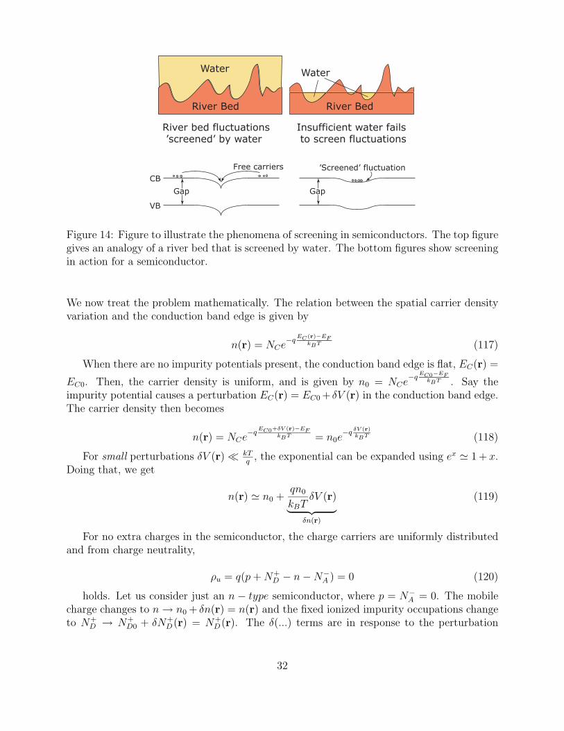
Water
River Bed
Water
River Bed
River bed fluctuations ’screened’ by water
Insufficient water fails to screen fluctuations
Free carriersCB
VB
Gap Gap
’Screened’ fluctuation
Figure 14: Figure to illustrate the phenomena of screening in semiconductors. The top figuregives an analogy of a river bed that is screened by water. The bottom figures show screeningin action for a semiconductor.
We now treat the problem mathematically. The relation between the spatial carrier densityvariation and the conduction band edge is given by
n(r) = NCe−q
EC (r)−EFkBT (117)
When there are no impurity potentials present, the conduction band edge is flat, EC(r) =
EC0. Then, the carrier density is uniform, and is given by n0 = NCe−q
EC0−EFkBT . Say the
impurity potential causes a perturbation EC(r) = EC0 + δV (r) in the conduction band edge.The carrier density then becomes
n(r) = NCe−q
EC0+δV (r)−EFkBT = n0e
−qδV (r)kBT (118)
For small perturbations δV (r) kTq
, the exponential can be expanded using ex 1 + x.Doing that, we get
n(r) n0 +qn0
kBTδV (r)︸ ︷︷ ︸
δn(r)
(119)
For no extra charges in the semiconductor, the charge carriers are uniformly distributedand from charge neutrality,
ρu = q(p+N+D − n−N−
A ) = 0 (120)
holds. Let us consider just an n − type semiconductor, where p = N−A = 0. The mobile
charge changes to n→ n0 + δn(r) = n(r) and the fixed ionized impurity occupations changeto N+
D → N+D0 + δN+
D (r) = N+D (r). The δ(...) terms are in response to the perturbation
32

δV (r), which is screening in action. The screened potential can be got by solving Poisson’sequation that relates charges to potentials -
∇2(EC0 + δV (r)) = −ρ(r)ε(0)
= −q(N+D + δN+
D (r)) − (n0 + δn(r))
ε(0)(121)
Flatband conditions take out the constant terms in the equation, and we are left withonly the δ(...) terms -
∇2δV (r) = −q(δN+D(r) − δn(r))
ε(0)(122)
Using our approximations δn(r) qn0
kBTδV (r) and δN+
D (r) −qN+D0
kBTδV (r), we get
∇2δV (r) =q2n
ε(0)kBTδV (r) =
1
λ2D
δV (r) (123)
Where we have defined λD =√
ε(0)kBTq2n , the Debye screening length. Here, n is an
effective carrier concentration that is effective in screening. It is generally not equal to thefree mobile carrier density. For a n-type sample the effective electron screening concentrationis given by
n = n+n(ND − n)
ND
(124)
For completely ionized non-degenerate carriers, it is a good approximation to assume thescreening electron density to be doping density, i.e., n = ND.
Now we have a equation that we can apply to solve for any fluctuating potential δV (r).For the special case of a spherically symmetric fluctuation (example, Coulombic potentialaround a charged donor), Equation 57 becomes
d2
dr2(rδV (r)) =
r
λ2D
δV (r) (125)
The solution for this equation for the Coulombic potential V (r) = q2
4πε0Kris the screened
potential V (r) = q2
4πε0Kre−r/λD . The Coulombic potential is thus ‘screened’ by the Yukawa
potential which reduces the potential very quickly within a few Debye lengths. We will usethis result in evaluating ionized impurity scattering rates later.
For two-dimensional electron gases, it turns out that screening is much weaker. There isa surprising result that the screening length is a constant independent of the 2DEG densityfor all practical purposes. The 2DEG screening length is called the Thomas-Fermi length,and is given by
λTF =2πε0Kh
2
q2m=a
B
2(126)
where aB is the effective Bohr radius in the semiconductor.
From the form of FGR, we see that the scattering potential U(r) always appears as amatrix element
33
U(q) = 〈k + q|U(r)|k〉 =∫d3re−iqrU(r)︸ ︷︷ ︸
FT (U(r))
(127)
where q = k′ − k. It is easy to see that this is nothing but the Fourier transform of thepotential U(r). Fourier transform is an extremely useful technique to solve such problems.To start off, let me state a very useful result10 - the 3D Fourier transform of the bare Coulombpotential U(r) = e2
4πε0ris given by
U(q) =e2
ε0q2(128)
For a semiconductor without free carriers, this is scaled by the static dielectric constantK - U(q) = e2
ε0Kq2 . Note that it diverges as q → 0 - this is indicative of the long-range natureof the Coulomb potential. We derive the Fourier transform for a screened Coulomb potentialUsc(r) = e2
4πε0Kre−r/λD in the following.
Usc(q) =∫d3eiq·rUsc(r) (129)
Align z − axis along q.
Usc(q) =e2
4πε2K
∫r2 sin(θ)drdθdφ
e− r
λD
reiqr cos(θ) (130)
Writing 1/λD = qD, and evaluating this integral gives us
Usc(q) =e2
ε0K(q2 + q2D)
=U(q)
ε(q)(131)
where ε(q) = 1 +q2D
q2 is a scaling factor that the bare Fourier transform can be divided
by to get the screened Fourier transform. qD = 1/λD is the Debye-Huckel wavevector. Notethat screening has removed the divergence as q → 0. Thus screening removes the long-rangecomponents of the Coulomb potential.
For a 2DEG, the Fourier Transform scaling factor after screening is given by
ε(q) = 1 +qTF
q(132)
where qTF = 1/λTF . Screening is weaker for a 2DEG than in 3D11. So the Fouriertransform of any screened Coulombic potential will be the Fourier transform of the barepotential divided by this factor.
10pg 350, John Davies11John Davies, pg 352
34

6.5 Screening by 2D/3D Carriers: Formal Theory
An important effect of the presence of mobile carriers in a semiconductor is screening. Sincewe are interested in scattering of mobile carriers from various defect potentials in the III-Vnitrides, we summarize the theoretical tool used to attack the problem of screening in thepresence of free carriers in the semiconductor.
The permittivity of vacuum is denoted as ε0. If a material has no free carriers, an externald.c. electric field E will be scaled due to screening by movement of electron charge clouds ofthe atoms and the nuclei themselves - this yields the dielectric constant of the material, ε(0).The electric field inside the material is accordingly scaled down to E/ε(0)ε0. If the electricfield is oscillating in time, the screening by atomic polarization becomes weaker since thenuclei movements are sluggish, and in the limit of a very fast changing field, only the electroncharge clouds contribute to screening, resulting in a reduced dielectric constant ε(∞) < ε(0).These two material constants are listed for the III-V nitrides in Table 1, and are relatedto the transverse and longitudinal modes of optical phonons by the Lyddane-Sachs-Tellerequation ε(0)/ε(∞) = ω2
LO/ω2TO [5].
The situation is more lively in the presence of mobile carriers in the conduction band[6]. In the situation where the perfect periodic potential of the crystal lattice is disturbedby a most general perturbing potential V (r)eiωte−Γt (the potential may be due to a defect,impurity, or band variations due to phonons), additional screening of the potential is achievedby the flow of the mobile carriers. Lindhard first attacked this problem and with a random-phase approximation (RPA), arrived at a most-general form of the relative dielectric constantε(q, ω) given by [7]
ε(q, ω) = ε(∞) + (ε(0) − ε(∞))ω2
TO
ω2TO − ω2
+ ε(0)Vuns(q)∑k
fk−q − fkhω + iΓ + εk−q − εk
. (133)
Here, the first two terms take into account the contributions from the nuclei, the coreelectron clouds, and the valence electron clouds. The last term has a sum running overthe free carriers only, and is zero for an intrinsic semiconductor. With this form of thedielectric function, the unscreened spatial part of the perturbation Vuns(q) gets screened toVscr = Vuns(q)/ε(q, ω). Here Vuns(q) is the Fourier-coefficient of the perturbing potentialV (q) =
∫ddreiqrV (r).
We are interested exclusively in static perturbations (defects in the material), and thusthe time dependent part ω, hω + iΓ → 0. With the approximations fk−q − fk ≈ −q · ∇kfkand εk−q − εk ≈ −h2q · k/m, the dielectric function may be converted to [5]
ε(q) = ε0(1 + V (q)∑k
∂f
∂ε), (134)
which is a very useful form that applies regardless of the dimensionality of the problem.For 2-dimensional carriers, a Coulombic potential V (r) which has the well-known Fourier
transform V2d(q) = e2/L2ε(0)ε0q, where L2 is the 2DEG area and q is the 2DEG wavevector[3], the dielectric function may be written as
ε2d(q) = ε(0)(1 +e2
qε(0)ε0
∂(∑
k fk/L2)
∂ε) = ε(0)(1 +
qTF
q). (135)
35

Since the factor in brackets is the sheet density∑
k fk/L2 = ns, we get the ‘Thomas-Fermi’
screening wavevector qTF given by
qTF =me2
2πε(0)ε0h2 =
2
aB
, (136)
aB being the effective Bohr-radius in the semiconductor. Thus, the screening in a perfect
2DEG is surprisingly independent of the 2DEG density, and depends only on the basicmaterial properties, within limits of the approximations made in reaching this result [8].For quasi-2DEGs, where there is a finite extent of the wavefunction in the third dimension,the dielectric function acquires form-factors that depend on the nature of the wavefunction.Finally, the screened 2-d Coulomb potential is given by
Vscr(q) =e2
ε0ε(0)(q + qTF ). (137)
Similarly, for the 3-d case, the Coulomb potential V (q) = e2/L3ε0ε(0)q2 leads to a dielec-tric function
ε3d(q) = ε(0)(1 +q2D
q2), (138)
where Debye screening-wavevector qD is given by
qD =
√√√√e2NcF−1/2(ζ)
ε0ε(0)kBT, (139)
for an arbitrary degeneracy of carriers.
6.6 Mobility of two- and three-dimensional carriers
6.6.1 Two-dimensional carriers
The wavefunction of electrons for band-transport12 in 2DEG is
〈r|k〉 =1√Aeik·rχ(z)unk(r), (140)
where the wavefunction is decomposed into a plane-wave part in the 2-dimensional x− yplane of area A and a finite extent in the z−direction governed by the wavefunction χ(z). k, rare both two-dimensional vectors in the x− y plane. unk(r) are the unit-cell-periodic Bloch-wavefunctions, which are generally not known exactly. The Kane model of bandstructurepresents an analytical approximation for the Bloch-functions [9], which is not presented inanticipation of the cancellation of the Bloch-function for transport in parabolic bands.
Assuming that the defect potential is given by V (r, z), which depends on both the in-planetwo-dimensional vector r and z perpendicular to the plane, time-dependent perturbation
12In the presence of heavy disorder, the wavefunctions are localized and transport occurs by hopping andactivation. For such cases, we cannot assume plane-wave eigenfunctions for electrons. All samples studiedhere are sufficiently pure, localization effects are neglected.
36

theory provides the solution for the scattering rate of electrons in the 2DEG. Scattering ratefrom a state |k〉 to a state |k′〉 is evaluated using Fermi’s Golden Rule [3]. The use of Fermi’sGolden rule in the δ−function form is justified since the typical duration of a collision in asemiconductor is much less than the time spent between collisions [7, 10]. The scatteringrate is written as
S(k,k′) =2π
h|Hk,k′|2δ(εk − εk′), (141)
where Hk,k′ = 〈k′|V (r, z)|k〉 · Ik,k′ is the product of the matrix element 〈k′|V (r, z)|k〉 ofthe scattering potential V (r, z) between states |k〉, |k′〉 and the matrix element Ikk′ betweenlattice-periodic Bloch functions. Owing to the wide bandgap of the III-V nitrides, thematrix element Ikk′ ≈ 1, the approximation holding good even if there is appreciable non-parabolicity in the dispersion [9].
By writing the scattering term in the form of Equation 141, we reach a point of connectionto the Boltzmann-transport equation. Once the matrix element is determined, the momen-tum relaxation time τm(k) of the single particle state |k〉 is evaluated from the solution ofthe Boltzmann-transport equation as
1
τm(k)= N2D
∑k′S(k′, k)(1 − cos θ), (142)
where N2D is the total number of scatterers in the 2D area A and θ is the angle ofscattering. Implicit in this formulation is the assumption that all scatterers act independentlyof each other, which is true if they are in a dilute concentration. If this does not hold (asin heavily disordered systems), then one has to take recourse to interference effects frommultiple scattering centers by the route of Green’s functions [11]. The impurity concentrationin AlGaN/GaN 2DEGs is dilute due to good growth control - this is confirmed by the bandtransport characteristics.
θk
k’qεF
kx
ky
Fermi circle
Γ-valley edge
E0
Figure 15: Visualization of the scattering process on the 2DEG Fermi-circle.
We write q = k − k′ as depicted in Figure 15. Since states for the subband with ε < εF
are filled, they do not contribute to transport. Transport then occurs by scattering in theFermi circle shown in the figure, and |k| = |k′| ≈ kF . From the figure, the magnitude of q
37

is q = 2kF sin(θ/2) where θ is the angle of scattering. This makes 1 − cos θ = q2/2k2F . As a
result, all integrals in the vector q reduce to integrals over angle θ.Any measurement of transport properties samples over all state |k〉 values. Converting
the summation to an integral over the quasi-continuous wavevector states and exploiting thedegenerate nature of the carriers for averaging τm(k), the measurable momentum scatteringrate 〈1/τm〉 reduces to the simple form [3]
1
〈τm〉 = nimp2D
m∗
2πh3k3F
∫ 2kF
0|V (q)|2 q2√
1 − ( q2kF
)2, (143)
where nimp2D = N2D/A is the areal density of scatterers and kF =
√2πns is the Fermi
wavevector, ns being the 2DEG density.The perturbation potential matrix element is given by
Vnm(q) =1
A
∫dz(χ
n(z)χm(z)∫d2rV (r, z)eiq·r
), (144)
where n,m are the subband indices. This reduces to
V (q) = V00(q) =1
AF (q)V (q, z0) (145)
when only the lowest subband (n = m = 0) is occupied. Here, F (q) is a form factorthat is unity when the 2DEG spread in the z−direction is a delta function. The scatteringpotential
V (q, z0) =Vuns(q, z0)
ε2d(q)(146)
is the screened two-dimensional Fourier transform of the scattering potential of a scattererlocated at z0 for a perfect 2DEG (no z−spread), where the screened-dielectric function(Equation 135) was used.
For accurate evaluation of transport properties and scattering rates, the finite extent ofthe 2DEG along the z direction must be accounted for. The exact form of the wavefunctionfrom the self-consistent Schrodinger - Poisson solution is very useful in determining the 2DEGsheet density and the shape of the wavefunction.
However, for analytic evaluation of scattering rates, the Fang-Howard variational wave-function is a better candidate, and has been used successfully for transport calculations inthe past [3]. The form of the wavefunction is
χ(z) = 0, z < 0
χ(z) =
√b3
2ze−
bz2 , z ≥ 0, (147)
where b is a variational parameter. The parameter is chosen such that it minimizes the
energy; this is achieved when b =(33m∗e2ns/8h
2ε0εb)1/3
, where ns is the 2DEG density. The
centroid of the distribution (which is also a measure of the spread) is 〈z〉 =∫∞0 z|χ(z)|2 = 3/b.
38

Thus, if the 2DEG z−dependence in not important in a scattering mechanism, the Fang-Howard function reduces to an ideal sheet charge ρ(z) → ensδ(z) when b→ ∞.
The Fang-Howard variational wavefunction leads to a form factor
F (q) = η3 = (b
b+ q)3. (148)
Screening by free carriers in the 2DEG is also affected due to the finite extent. This isreflected in another form factor G(q) entering the 2D dielectric function
ε2d(q) = ε(0)(1 +qTF
qG(q)). (149)
The screening form factor G(q) is given by
G(q) =1
8(2η3 + 3η2 + 3η), (150)
and qTF is the Thomas-Fermi screening wavevector [8]. For a perfect 2DEG with noz−spread, η → 1, and both form factors F (q), G(q) reduce to unity. Thus, the Fang-Howardapproximation along with particular scattering potentials can be used for evaluating thescattering rates of electrons in AlGaN/GaN 2DEGs.
6.6.2 Three-dimensional carriers
The generalized formula for mobility (Equation 107) applied to three-dimensional carriers(d=3) reduces to
µ3d =eτ0m
Γ(n+ 52)
Γ(52)
Fn+ 12(ζ)
F 12(ζ)
=2eτ0
3mn3d
Γ(n+5
2)Fn+ 1
2(ζ), (151)
where n3d = N3dc F1/2(ζ).
Once τ0 is known for a scattering mechanism, ζ can be used from the Joyce-Dixon approx-imation (Equation 115) to calculate the mobility. Momentum scattering rates for varioustypes of scattering mechanisms are well known ([1, 5, 2]). Mobility for some scatteringmechanisms is now found used these scattering rates.
• Deformation potential Scattering
The deformation potential acoustic phonon momentum relaxation time is given by
τac =2πh4ρv2
s
(2m)32a2
C
ε−1/2
kBT, (152)
where the exponent n = −1/2, aC is the conduction-band edge deformation potential,and ρ, vs are the mass density and the sound velocity in the material respectively.Using this, and the fact that F0(ζ) = ln(1 + eζ), acoustic-phonon scattering limiteddrift mobility becomes
39

µac =2ehρv2
s
3πn3dma2C
ln(1 + eζ), (153)
where ζ = εF/kBT . This is a convenient closed-form expression for evaluation ofmobility. The expression holds for an arbitrary degeneracy at arbitrary temperatures,which makes it much more useful than the traditionally used form of strongly non-degenerate limit. It is fortuitous that this form of mobility could be derived - itholds for all scattering mechanisms whose scattering rates have an energy exponent ofn = −1/2.
The traditional expression for deformation-potential acoustic phonon scattering limitedmobility in semiconductors in the strongly non-degenerate limit (ζ −1) is
µNDac =
2√
2πeh4ρv2s
3(m)5/2a2C(kBT )3/2
, (154)
with a T−3/2 dependence. On the other extreme, for a strongly degenerate populationof carriers, the mobility is
µDac =
(π/3)1/3eh3ρv2s
(m)2a2Cn
1/33d (kBT )
, (155)
which is different from the non-degenerate case in the temperature dependence, and acarrier concentration dependence. Care needs to be exercised in using the expressionfor the strongly degenerate regime - if the acoustic phonon energy hvsk is larger thanthe thermal energy kBT which becomes very small at low temperatures, then the resultdoes not hold since the phonon number cannot be approximated by kBT/hvsk.
• Piezoelectric phonon Scattering
For piezoelectric phonon scattering, the relaxation rate is given by
τpz =2√
2πh2ρv2s
(m)1/2(ehpz/ε)2
ε+1/2
kBT, (156)
where ehpz/ε is the piezoelectric coefficient. Generalized mobility expression yields
µpz =16eρv2
s(kBT )
3πnh(ehpz/ε)2× F1(ζ), (157)
which is in a form that may be evaluated numerically.
For the strongly non-degenerate case, we get the mobility as
µNDpz =
16√
2πeh2ρv2s
3(ehpz/ε)2(m)3/2(kBT )1/2, (158)
40

which is the classical value quoted in texts [5] with the T−1/2 dependence. In thestrongly degenerate regime, we get
µDpz =
2(3π5)13 eh3ρv2
sn1/33d
(ehpz/ε)2(m)2(kBT ). (159)
• Ionized Impurity Scattering
Ionized impurity scattering time is given by [5]
τimp =16πε2(2m)1/2
e4NIK0
× ε3/2, (160)
where NI is the ionized impurity density and K0 is a weak function of energy, and maybe assumed constant in the calculations. Mobility is given by
µimp =128mε2(kBT )3
h3e3NIK0n× F2(ζ). (161)
In the non-degenerate case, we recover the traditional Brooks- Herring formula
µNDimp =
128√
2πε2
e3NIK0(m)1/2× (kBT )3/2, (162)
with the T 3/2 dependence. For strongly degenerate carriers, we get
µDimp =
24π3ε2h3n3d
e3NIK0(m)2, (163)
which is weakly temperature dependent (through K0), but now dependent on the 3dcarrier density.
• Alloy Scattering
For alloy scattering, the momentum relaxation rate is given by [5]
τalloy =2πh
V 20 Ω[x]x(1 − x)(2m/h2)3/2
× ε−1/2, (164)
where V0 is the alloy-scattering potential, x is the alloy composition, and Ω[x] is thevolume range of the alloy-scattering potential. This is again with an exponent ofn = −1/2. Using the techniques developed till now, we get the formally exact alloyscattering limited mobility to be
µalloy =2eh
3πmV 20 Ωx(1 − x)
kBT
n3d
ln(1 + eζ). (165)
We get the classical non-degenerate limit of mobility to be
41

µNDalloy =
2√
2eh4
3(m)5/2V 20 Ωx(1 − x)(kBT )1/2
, (166)
and the degenerate limit as
µDalloy =
(π/3)1/3eh3
(m)2V 20 Ωx(1 − x)n
1/33d
, (167)
where the degenerate nature of scattering removes the temperature dependence andadds a weak carrier density dependence.
• Polar optical phonon scattering
Polar optical phonon scattering limited mobility is given by
µPOP =4πε0ε
h
emNbose(T )q0, (168)
where 1/ε = 1/ε∞ − 1/ε0, the phonon-wavevector is given by hωop = h2q20/2m
, andNB(T ) = 1/(exp[hωop/kBT ] − 1) is the Bose-Einstein distribution function.
6.7 Material properties of III-V nitrides relevant to transport
For the calculation of transport properties of the III-V nitride semiconductors, it is essentialto know various properties of the material. The bandstructure is of utmost importance,determining the effective mass of carriers and the allowed energy and momentum eigenvaluesfor the carriers. The band-alignment is essential for analyzing transport of quantum-confinedcarriers at heterojunctions. The electro-mechanical properties such as deformation potentialsof the bands and acoustic wave (sound) velocities are essential in the electron-acoustic phononcoupling study. Optical deformation potential and optical phonon energies are essential incalculating optical phonon scattering rates. In what follows, these properties are surveyedfor the III-V nitride semiconductors with an eye for application for transport studies.
Bandstructure and alignmentSince we are interested in analyzing transport in GaN, a close look at the bandstructure
is in order. In Figure 2, the Brillouin zone, the theoretically calculated Bandstructure [12]and the simplified bandstructure [13] with only the lowest three conduction band valleys areshown.
Carriers residing in the lowest conduction-band valley (Γ-valley, direct gap) have aneffective mass of m = 0.2m0. The next band minimum is in the M − L direction of theBrillouin zone at 2.1 eV from the Γ point. The effective mass of carriers in this valleyis m
ML = 0.4m0. From the Brillouin-zone picture, there are six such equivalent minima.The next minimum is close to the M − L minimum in energy - it is at the A-point in theBrillouin-zone. The effective mass in this valley is m
A = 0.6m0. We note here that theeffective masses and energy separations of the M − L and A valleys are from theoreticalbandstructure calculations [13] whereas that of the Γ valley has been verified experimentally([14, 15]).
42

Table 1: Material properties of GaN for transport calculations [17]
Property Symbol GaN AlN InN Units
Effective mass (Γ valley) m 0.2 0.5 0.1 m0
Mass density ρ 6.15 3.23 6.81 g/cm−3
Static dielectric constant ε(0) 8.9 8.5 15.3 -High frequency dielectric constant ε(∞) 5.35 4.77 8.4 -
Optical phonon energy hωop 92 100 89 meVDeformation potential Ξ 8.3 9.5 7.1 meV
Sound velocity (Longitudinal) vs 8 11 5.2 105 cm/s
The large separation of the direct-gap Γ valley minima from the other minima at A,L−M (∆ε ≥ 1 eV) bodes well for low-field transport analysis; a parabolic dispersion ε =h2k2/2m is a good approximation. The effective mass is m = 0.2m0, and has been reportedto be isotropic [16], which simplifies the transport analysis. Figure 16 depicts the banddiscontinuities between the three members of the nitride family - InN, GaN, and AlN.
AlN GaN InN
2.1eV
0.7eV
6.2eV
3.4eV0.8eV
0.65eV
1.95eV
Ec
Ev
Figure 16: The band alignment in the III-V nitrides. Note that the fundamental bandgap ofInN was previously believed to be 1.9eV - measured on heavily doped polycrystalline films.However, developments in growth techniques only recently made it possible to grow puresingle crystals which lead to the new bandgap. The band alignment of InN is assumed tofollow the same 3:1 ratio as in the case of GaN and AlN; it has not been experimentallymeasured yet.
The phonon dispersion curves of GaN have been calculated theoretically and measuredexperimentally as well. The experimental determination of phonon dispersion curves istraditionally done by the technique of neutron scattering. However, this technique requiresunstrained samples of large sizes, which has not been possible till date. Bulk unstrainedGaN samples of GaN can be grown by high pressure techniques, however, these samplesare small in size (5 × 5mm). Ruf et. al. [18] overcame the size limitation by using the
43

Γ ΑΑ
L-O branch
L-A branch
ω
kω~vsk
ω~ω092meV
vs=8x105cm/s
GaN phonon dispersion (simplified model)
Brillouin zone edge
Figure 17: Phonon dispersion of GaN with the two parameters needed for transport studies.
similar technique of inelastic X-Ray scattering for determining the phonon-dispersion of thematerial. They found very close agreement between the measured phonon-dispersion andthe calculated dispersions by ab-initio techniques.
Since our interest in this work is aimed towards determining the electron-phonon couplingfor transport calculations, we use the simplified phonon-dispersion shown in Figure 17. Thepresence of both longitudinal and transverse modes of phonon propagation complicates theusage - we will assume only the longitudinal components since the effect of the transversemodes is much weaker.
The longitudinal sound velocities are given by vs =√c11/ρ and vs =
√c3/ρ for the [1000]
and [0001] directions of the wurtzite lattice. Since c11 ∼ c33 for GaN, AlN, and InN, it is agood approximation to assume that sound velocity is isotropic along the two directions; thesound velocities are tabulated in Table 1. Since acoustic phonons couple to electrons in thesemiconductor through the deformation potential, the deformation potentials of the lowestconduction band valley are also listed in Table 1.
7 Current research, future directions
I list some topics of intense current interest. These are related to topics on transport theorycovered in the class and you should be able to read papers related to these topics -
• Transport of electrons in 2DEGs - The integral and fractional quantum Hall effects. Ithas already generated four Physics Nobel prizes.(Von Klitzing, Stormer, Tsui, Laugh-lin).
44

• Transport in Disordered electronic systems - Metal-Insulator transistions in bulk and2DEGs, Localization, etc. Has garnered at least 2 Physics Nobel prizes.(Mott, Ander-son).
• Ballistic transport through quantum point contacts, quantized conductance.
• Transport in Quantum Wires, Dots.
• Transport in Nanotubes and Nanowires.
• Spin transport and spin scattering in dilute magnetic semiconductors.
References
[1] K. Seeger, Semiconductor Physics, An Introduction. Berlin: Springer Verlag, 6th ed.,1999.
[2] C. M. Wolfe, N. Holonyak Jr., and G. E. Stillman, Physical Properties of Semiconduc-tors. Englewood Cliffs, New Jersey: Prentice Hall, 1st ed., 1989.
[3] J. H. Davies, The Physics of Low-Dimensional Semiconductors. Cambridge, UnitedKingdom: Cambridge University Press, 1st ed., 1998.
[4] W. B. Joyce and R. W. Dixon Appl. Phys. Lett., vol. 31, p. 354, 1977.
[5] C. Hamaguchi Basic Semiconductor Physics, p. 280, 2001.
[6] J. Ziman Theory of Solids, Cambridge University Press, 1972.
[7] D. K. Ferry, Semiconductor Transport. London: Taylor & Francis, 1st ed., 2000.
[8] T. Ando, A. B. Fowler, and F. Stern Rev. Mod. Phy., vol. 54, p. 437, 1982.
[9] B. M. Askerov, Electron Transport Phenomena in Semiconductors. Singapore: WorldScientific, 1st ed., 1994.
[10] H. Kroemer, Quantum Mechanics for Engineering, Materials Science, and AppliedPhysics. Englewoods Cliff, New Jersey: Prentice Hall, 1st ed., 1994.
[11] G. D. Mahan, Many Particle Physics. New York: Kluwer Academic/Plenum Publishers,3rd ed., 2000.
[12] S. Bloom, G. Harbeke, E. Meier, and I. B. Ortenburger Phys. Stat. Solidi, vol. 66, p. 161,1974.
[13] U. Bhapkar and M. S. Shur J. Appl. Phys., vol. 82, p. 1649, 1997.
[14] A. F. Brana, C. Diaz-Paniagua, F. Batallan, J. A. Garrido, E. Munoz, and F. OmnesJ. Appl. Phys., vol. 88, p. 932, 2000.
45
[15] W. Knap, S. Contreras, H. Alause, C. Skierbiszewski, J. Camassel, M. Dyakonov, J. L.Robert, J. Yang, Q. Chen, M. A. Khan, M. L. Sadowski, S. Huant, F. H. Yang, M. Goian,J. Leotin, and M. S. Shur Appl. Phys. Lett., vol. 70, p. 2123, 1997.
[16] I. Vurgaftman, J. R. Meyer, and L. R. Ram-Mohan J. Appl. Phys., vol. 89, p. 8815,2001.
[17] E. archive New Semiconductor Materials Characteristics and Propertieshttp://www.ioffe.rssi.ru/SVA/NSM/.
[18] T. Ruf, J. Serrano, M. Cardona, P. Pavone, M. Pabst, M. Krisch, M. D’Astuto, T. Suski,I. Grzegory, and M. Leszczynski Phys. Rev. Lett., vol. 86, p. 906, 2001.
46