charge carrier recombination dynamics in hybrid metal
TRANSCRIPT

Charge Carrier Recombination
Dynamics in Hybrid Metal Halide
Perovskite Solar Cells
Dissertation zur Erlangung des
naturwissenschaftlichen Doktorgrades
der Julius-Maximilians-Universität Würzburg
vorgelegt von
David Kiermaschaus Pleß, Polen
Würzburg 2020

Eingereicht am: 19.03.2020
bei der Fakultät für Physik und Astronomie
1. Gutachter: Prof. Dr. Vladimir Dyakonov
2. Gutachter: Prof. Dr. Christian Schneider
3. Gutachter:
der Dissertation
Vorsitzende(r):
1. Gutachter: Prof. Dr. Vladimir Dyakonov
2. Gutachter: Prof. Dr. Christian Schneider
3. Gutachter: Prof. Dr. Karl Mannheim
im Promotionskolloquium
Tag des Promotionskolloquiums: 15.07.2020
Doktorurkunde ausgehändigt am:
ii

Contents
1. Introduction 1
2. Hybrid Halide Perovskites for Photovoltaic Applications 5
2.1. Crystal Structure . . . . . . . . . . . . . . . . . . . . . . . . . . . . . . . . . . 5
2.2. Optoelectronic Properties . . . . . . . . . . . . . . . . . . . . . . . . . . . . . 8
2.3. Perovskite Photovoltaics . . . . . . . . . . . . . . . . . . . . . . . . . . . . . . 14
2.3.1. Device Layout and Working Principle . . . . . . . . . . . . . . . . . . 14
2.3.2. Current-Voltage Characterization and Photovoltaic Performance . . 18
2.3.3. Hysteresis Effects . . . . . . . . . . . . . . . . . . . . . . . . . . . . . . 22
3. Charge Carrier Recombination in Semiconductors 29
3.1. Recombination Mechanisms . . . . . . . . . . . . . . . . . . . . . . . . . . . 29
3.1.1. Shockley-Read-Hall Recombination . . . . . . . . . . . . . . . . . . . 31
3.1.2. Radiative Recombination . . . . . . . . . . . . . . . . . . . . . . . . . 35
3.1.3. Auger Recombination . . . . . . . . . . . . . . . . . . . . . . . . . . . 37
3.2. Charge Carrier Lifetimes . . . . . . . . . . . . . . . . . . . . . . . . . . . . . . 38
3.3. Relationship between Recombination and PV Parameters . . . . . . . . . . 39
4. Experimental Methods 45
4.1. Materials . . . . . . . . . . . . . . . . . . . . . . . . . . . . . . . . . . . . . . . 45
4.2. Device Preparation . . . . . . . . . . . . . . . . . . . . . . . . . . . . . . . . . 48
4.3. Transient Electrical Techniques . . . . . . . . . . . . . . . . . . . . . . . . . . 52
4.3.1. Open-Circuit Voltage Decay . . . . . . . . . . . . . . . . . . . . . . . . 53
4.3.2. Transient Photovoltage . . . . . . . . . . . . . . . . . . . . . . . . . . 54
4.3.3. Charge Extraction . . . . . . . . . . . . . . . . . . . . . . . . . . . . . . 56
5. Capacitive Eects in Transient Electrical Measurements 59
5.1. Introduction . . . . . . . . . . . . . . . . . . . . . . . . . . . . . . . . . . . . . 60
5.2. Devices and Current-Voltage Characteristics . . . . . . . . . . . . . . . . . . 63
5.3. Determination of Charge Carrier Lifetimes . . . . . . . . . . . . . . . . . . . 65
5.4. Effect of External Conditions on Voltage Decay . . . . . . . . . . . . . . . . 67
5.5. Analytical Description of OCVD and Lifetimes . . . . . . . . . . . . . . . . . 74
iii

Contents
5.6. Impact of Capacitive Effects on Charge Carrier Density . . . . . . . . . . . . 82
5.7. Summary . . . . . . . . . . . . . . . . . . . . . . . . . . . . . . . . . . . . . . . 86
6. Bulk Recombination in MAPbI3 Solar Cells Revealed by Active Layer
Thickness Variation 89
6.1. Introduction . . . . . . . . . . . . . . . . . . . . . . . . . . . . . . . . . . . . . 90
6.2. Devices and Current-Voltage Characteristics . . . . . . . . . . . . . . . . . . 92
6.3. Relation between Charge Carrier Density and Open-Circuit Voltage . . . . 98
6.4. Relation between Charge Carrier Lifetime and Open-Circuit Voltage . . . . 101
6.5. Charge Carrier Dynamics and Recombination Order . . . . . . . . . . . . . 104
6.6. Transient and Steady-State Parameters . . . . . . . . . . . . . . . . . . . . . 106
6.7. Summary . . . . . . . . . . . . . . . . . . . . . . . . . . . . . . . . . . . . . . . 109
7. Improved Open-Circuit Voltage of Evaporated Perovskite Solar Cells
by Post-Annealing 111
7.1. Introduction . . . . . . . . . . . . . . . . . . . . . . . . . . . . . . . . . . . . . 112
7.2. Devices and Current-Voltage Characteristics . . . . . . . . . . . . . . . . . . 114
7.3. Ideality Factor from Current-Voltage Characteristics in the Dark . . . . . . 117
7.4. Analysis of Charge Carrier Lifetimes . . . . . . . . . . . . . . . . . . . . . . . 120
7.5. External Quantum Efficiency of Electroluminescence . . . . . . . . . . . . 124
7.6. Discussion . . . . . . . . . . . . . . . . . . . . . . . . . . . . . . . . . . . . . . 125
7.7. Summary . . . . . . . . . . . . . . . . . . . . . . . . . . . . . . . . . . . . . . . 127
8. Impact of Active Area Masking on Current-Voltage Characterization
of Solar Cells 129
8.1. Introduction . . . . . . . . . . . . . . . . . . . . . . . . . . . . . . . . . . . . . 130
8.2. Current-Voltage Characteristics . . . . . . . . . . . . . . . . . . . . . . . . . . 132
8.3. Influence on Open-Circuit Voltage . . . . . . . . . . . . . . . . . . . . . . . . 133
8.4. Influence on Fill Factor . . . . . . . . . . . . . . . . . . . . . . . . . . . . . . . 137
8.5. Consequences for the Power Conversion Efficiency . . . . . . . . . . . . . . 141
8.6. Summary . . . . . . . . . . . . . . . . . . . . . . . . . . . . . . . . . . . . . . . 143
9. Summary 145
9.1. Zusammenfassung . . . . . . . . . . . . . . . . . . . . . . . . . . . . . . . . . 148
Bibliography 152
A. Publications and Conference Contribution 195
B. Danksagung 197
iv

1. Introduction
The Need for Renewable Energy Sources
There is conclusive evidence that the increase in the Earth’s temperature and the fast
disappearance of snow and ice over the past decades are largely caused by the human
influence on the greenhouse effect, which describes the atmosphere’s ability to trap
the emitted radiation from the planet’s surface. The industrial revolution in combina-
tion with the population growth caused a dramatic rise of greenhouse gases like carbon
dioxide (CO2), methane (CH4) and nitrous oxide (N2O) over the last centuries. For ex-
ample, the CO2 concentration in the atmosphere has increased by more than 40 % from
280 ppm to 400 ppm since 1850. [1] These gases absorb energy in the infrared range
of the electromagnetic spectrum and therefore have a huge impact on the observed
global warming by intensifying the greenhouse effect. To counteract this process and
limit the anthropogenic temperature increase to a maximum of 2 °C on average above
pre-industrial levels, 197 nations negotiated an arrangement at the United Nations Cli-
mate Change Conference 2015. [2] To this date, more than 180 parties have already rat-
ified to the so-called Paris Agreement. [3] To reach the goal of a maximum temperature
increase of 2 °C, net zero CO2 emissions until 2060 to 2070 are required. [4] It has been
even suggested that the mean average should be limited to a lower value of 1.5 °C in or-
der to reduce the climate-related risks for nature and mankind. [5] Calculations revealed
that the existing energy infrastructure will exceed the remaining carbon budget for the
1.5 °C target if operated as historically. More than half of these emissions originate
from fossil fuel-burning power plants, [6] which illustrates that the expansion of power
plants based on renewable and environmental friendly energy sources will be of cen-
tral importance for the civilization in the coming decades. Many nations are already
focusing on increasing the contribution of renewable energy sources to power gener-
ation. In 2018, almost 35 % of the total power generation in Germany was produced
by renewable energy sources. Out of these renewables, photovoltaic (PV) installations
are among the largest clean energy sources with a market share of 20.5 %. [7] PV sys-
tems have great advantages over other energy sources such as direct access to sunlight
over the entire Earth. The utilization of sunlight would easily cover the world’s energy
demand, which explains the intensified research on solar cells in recent decades.
1

1. Introduction
Generations of Photovoltaic Devices
Today, the PV market is almost exclusively dominated by silicon (Si) as a photoac-
tive layer. Solar cells of this type can be manufactured from silicon of different de-
grees of crystallinity. Under laboratory conditions, monocrystalline devices can reach
power conversion efficiencies (PCEs) up to 26.3 %, [8] while polycrystalline silicon has
a slightly lower record PCE of 21.9 % [9] due to losses at grain boundaries. Despite the
lower efficiency, the majority of installed PV systems are polycrystalline. [10] As a conse-
quence of long research activities and improved economies of scale, the dominance of
Si-based solar systems can be explained by the rapid decline in prices over the previous
decades. [11]
Nevertheless, research is also focused on other material systems and technologies as
illustrated in Figure 1.1. While crystalline silicon solar cells belong to the 1st generation
of PVs, the 2nd generation can be described as a thin-film technology since the active
layer thickness of these devices is reduced from hundreds to a few micrometers. Well-
known representatives of this generation include cadmium telluride (CdTe), gallium
arsenide (GaAs) and copper indium gallium (di)selenide (CIGS). Although GaAs cells
are expensive which is one of the main reasons why they are not widely used, they cur-
rently hold the world record in efficiency for a single-junction solar cell at 29.1 %. [11]
Latest solar cell concepts are partially based on even thinner active layers in the range
of a few hundred nanometers composed of organic or hybrid organic-inorganic mate-
rials. These devices are referred to as 3rd generation solar cells. The pioneers of this
generation were the so-called dye-sensitized solar cells (DSSCs) and organic photo-
voltaics (OPVs). The former were introduced in 1991 by O’Regan and Graetzel by com-
bining titanium dioxide (TiO2) with a charge-transfer dye to sensitize the light harvest-
ing layer. [12] Although research on organic semiconductors has been going on for many
years, a major breakthrough for OPVs was the combination of two organic films leading
to an acceptor-donor interface which paved the way to efficient organic solar cells. [13]
Over the past decades, fullerenes and their derivates have been predominantly used
as electron acceptor materials for organic solar cells. Very recently, fullerene-free ac-
ceptors with higher absorption coefficients have been proposed to increase the device
performance. [14,15] With these newly synthesized acceptor materials, state-of-the-art
OPVs can reach efficiencies of more than 15 %. [16]
Another technology that is part of the 3rd generation of PVs are perovskite solar cells.
Since the first use of a perovskite absorber in 2009, [17] solar cell research was domi-
nated by this class of semiconductors. Starting with a PCE of 3.8 % in a DSSC config-
uration, the efficiency quickly climbed to 10 % in the following years when the liquid
electrolyte was replaced by a solid-state transport layer. [18,19] Further improvements in
2

3rd Generation:Organic / Hybrid
2nd Generation:Thin-Film
1st Generation:Silicon
Photovoltaics
amorphousSilicon
polycrystallineSilicon
monocrystallineSilicon CdTe / GaAs
CIGS
DSSC
Organic
Perovskite
Figure 1.1.: Three generations of existing PV technologies.
material composition, the introduction of new device configurations with novel trans-
port/interface layers and optimizations in the film formation led to a current record
PCE of 25.2 %. [20] Within only ten years of intensive research, the efficiency of these
devices has improved faster than ever before in the history of PVs. Despite the great
attention paid to this technology, there are still many unsolved problems. The solar
cells still suffer from a deficiency in long-term stability and also the use of toxic mate-
rials should be minimized. More importantly, the understanding of the basic physical
properties and working principles of these devices is still largely missing and prevents
further rise in efficiency. As a recent study emphasized, the greatest potential for fur-
ther PCE improvements is to minimize charge carrier recombination losses. [21] How-
ever, carrier dynamics are – so far – mostly studied on pure films, whereas very little is
known about recombination processes in fully operational devices as it is not straight-
forward to address this fundamental topic. This can be explained by the fact that solar
cells are complicated devices composed of a multitude of different layers complicating
the application and interpretation of the experimental methods.
Outline of the Thesis
The aim of this thesis is to contribute to a better understanding of recombination losses
in fully working perovskite solar cells and the experimental techniques which are ap-
plied to determine these losses. Chapter 2 focuses on introducing the class of lead
halide perovskite semiconductors and their application in PV devices. Chapter 3 ad-
dresses the main charge carrier recombination mechanisms and provides physical back-
ground for the interpretation of the herein performed measurements. The experimen-
tal background on the preparation of perovskite solar cells, the used materials and the
measurement methods are summarized in Chapter 4. The main experimental results
3

1. Introduction
are then divided into four individual and separate studies. Chapter 5 sheds a light on
the experimental techniques and provides new insights for the interpretation of the re-
sults obtained by these methods. Based on these findings, recombination dynamics
under operating conditions are identified in perovskite solar cells in Chapter 6 by vary-
ing the absorber thickness. With the aim of reducing charge carrier losses, Chapter 7
investigates the impact of post-annealing on the performance and the recombination
kinetics in vacuum deposited PV devices. Chapter 8 provides a detailed analysis on
the commonly applied method of masking the active area during characterization of
perovskite solar cells.
4

2. Hybrid Halide Perovskites for
Photovoltaic Applications
This chapter provides a detailed overview on the material class of hybrid metal halide
perovskites and their application as photoactive materials in solar cells. First, a short
insight into the crystal structure is given and the precursor materials for perovskite
synthesis are discussed. Afterwards the optoelectronic properties are described, which
underline the suitability for PV applications. Finally, solar cells based on metal halide
perovskites will be discussed in more detail including the device layout and current-
voltage characterization.
2.1. Crystal Structure
The term ’perovskite’ originally derives from the mineral calcium titanium oxide (CaTiO3)
discovered by the Prussian mineralogist Gustav Rose in 1839 in the Ural Mountains and
named in honor of Lev A. Perowski. [22] Today’s perovskites, which are implemented
in solar cells have very little in common with that mineral except for their ABX3 crys-
tal stoichiometry. In case of photoactive absorbers, A is usually a large cation, B is a
smaller metallic cation and X is an halogen anion. These metal halide perovskites were
first described in 1893, [23] long before the solar cell was invented. As shown in Figure
2.1, the inorganic BX3 sublattice is arranged in an octahedron and stabilized by the
A-site cation which has to be small enough to fit in the interstices. During the inten-
sive research over the last years, many different ion combinations have been identified
for the use in optoelectronic applications. In most cases, lead or tin represent the B
cation in the oxidation state +2 (Pb2+ or Sn2+) at the body-center of a unit cell, while
the face-centered X positions are halides such as I−, Br− or Cl− which are arranged
in an octahedron. Organic molecules like methylammonium (CH3NH3+, abbreviated
with MA+) and formamidinium (CH5N2+, abbreviated with FA+) and inorganic atoms
like Cs+ can be located at the corner positions. The most popular compound, studied
also in the first publication of a perovskite solar cell, is methylammonium lead iodide
(MAPbI3) which crystallizes in a tetragonal symmetry at room temperature where two
5

2. Hybrid Halide Perovskites for Photovoltaic Applications
A: MA+, FA+, Cs+
B: Pb2+, Sn2+
X: I-, Br-
a
bc
Figure 2.1.: Schematic illustration of the ABX3 perovskite crystal structure. Inorganic BX3
octahedra form a 3D lattice with the empty spaces being filled by the larger A cation.Widely used components for the preparation of PV devices are also listed, wherebythe most frequently studied combination is MAPbI3. In addition to the tempera-ture, the choice of the materials determines the symmetry in which the perovskite isformed.
lattice constants a and b are of the same value and smaller than the third lattice con-
stant c (a = b = 8.86A < c = 12.66A). [24] If MAPbI3 is heated to over about 327 K degrees,
a cubic crystal structure (a = b = c = 6.33 A) is formed, while an orthorhombic crystal
is present for temperatures below about 161 K (a = 8.86 A, b = 8.58 A, c = 12.62 A). [25–29]
While the cubic structure has the highest symmetry, both tetragonal and orthorhom-
bic phases are formed by tilting the PbI64 – octahedron around the c-axis resulting in a
reduced symmetry.
In general, the crystal structure is not only a function of temperature but is strongly
influenced by the radii of the individual ions. To predict the structure, distortion and
stability of the crystal, the tolerance factor t
t = r A + rXp2(rB + rX )
(2.1)
was proposed by Goldschmidt in the 1920s, where r A, rB and rX are the radii of the A,
B and X ions, respectively. [30] Most perovskites are characterized by a t value rang-
ing from 0.7 to 1.1. To form a cubic crystal phase, t must be in the range of 0.9 -
1.0, while it takes lower values in the case of less symmetric lattice structures. [31] With
r A = 0.180 nm for the MA+ cation, rB = 0.132 nm for the Pb2+ cation and rX = 0.206 nm
for the I− anion, t can be calculated to be 0.81 for MAPbI3 in line with the tetragonal
crystal phase at room temperature. [27] It is reported, that the tolerance factor is not
sufficient enough to make reliable statements if a stable perovskite can be formed. [32]
6

2.1. Crystal Structure
Since the BX6 octahedron defines the basic unit for the perovskite structure, the octa-
hedral factor µ
µ= rB
rX(2.2)
was introduced as an additional criterion. [33] It usually takes values in the range of
0.44 < µ < 0.89 and reliably predicts, in combination with t , the formation of a per-
ovskite lattice. If µ is smaller than 0.44, no BX6 octahedron and consequently no per-
ovskite structure can be formed. For MAPbI3, µ= 0.54 which verifies the stability of the
compound.
Both the tolerance factor and the octahedral factor developed to widely used quan-
tities in the material screening of new ions for the synthesis of light-absorbing per-
ovskites. The successful story was triggered by the combination of different ions, such
as the mixing of iodide and bromide in MAPb(I1−xBrx)3. [34] In addition to the exchange
of halides, many researchers tried to find new A-site cations as well. A major break-
through was the alloying of MA+ and FA+ cations in (FAPbI3)1−x(MAPbBr3)x stochiome-
tries leading to the first reported efficiencies of around 20 %. [35–37] This material com-
position turned out to be also beneficial for the long-term stability, since it is reported
for pure FAPbI3 that two polymorphs with quite different material characteristics exist
at room temperature: a black perovskite material and a yellow non-perovskite counter-
part. [38] A reduction of the undesirable yellow phase impurities was enabled by the the
introduction of Cs+ into mixed cation/mixed halide perovskites. [39,40] Scientists have
exploited the diversity of the periodic table even further and used additional elements
in the synthesis such as the alkali metal ions Rb+ or K+. These ions are expected to be
too small to form a stable perovskite crystal lattice if they are the only A-site cations
in the system. Nevertheless, they can be incorporated into so-called quadruple cation
perovskites which also include MA+, FA+ and Cs+. [41,42] However, NMR studies sug-
gest that only cesium may be integrated into the lattice, while the other smaller cations
are not part of the crystalline framework. [43] With the aim of increasing the stability
also larger organic cations like guanidinium (CH6N3+) were added to MAPbI3. [44] As
the only A-site cation in the perovskite, they would yield a tolerance factor above 1 and
the formation of a two-dimensional crystal lattice for which reason they can only be
used in mixed perovskites. There are also great efforts to replace lead with less toxic
or even non-toxic metals like tin or bismuth, but these have not been successful yet as
the efficiencies are not yet adequate. [45,46] As a consequence of the compositional en-
gineering during the last years, multi-cation perovskites comprising different halides
are among the most stable and efficient perovskite solar cells so far.
7

2. Hybrid Halide Perovskites for Photovoltaic Applications
2.2. Optoelectronic Properties
Before the first application in solar cells, perovskites were utilized in many different
applications. For example, the class of oxide perovskites like barium titanate (BaTiO3)
are known for their ferroelectric, piezoelectric, dielelectric and pyroelectric character-
istics. [47,48] Bednorz and Müller have also discovered superconducting properties at
high temperatures in some perovskite compounds and were awarded the Nobel Prize
for their work in 1987. [49] Although known since more than 100 years and extensively
analyzed for magnetic, optical and electronic properties, the last decade has sparked
an unprecedented interest in the family of perovskites.
Band Structure, Absorption and Charge Carrier Generation
The class of metal halide perovskites, where the commonly used oxide anions are re-
placed by halide anions shows semiconducting properties that are a precondition for
PV applications. It is exclusively the anorganic PbI64 – cage that leads to the forma-
tion of the valence and conduction bands (VB and CB, respectively) and an electronic
band gap as it is schematically depicted in Figure 2.2a. The valence band maximum
(VBM) consists of a Pb(6s) - I(5p) σ-antibonding (σ∗) orbital with the iodide orbital
being the dominant one. The conduction band minimum (CBM) is composed of a
Pb(6p) - I(5p) σ∗ orbital, where most of the empty states originate from the lead. [50–52]
This is in line with the formal electronic configuration of the ions in the lead iodide
octaedron: 5d106s26p0 for Pb2+ and 5p6 for I−. The fully occupied 5p6 orbitals from the
iodide are therefore relevant for the VBM, while empty 6p0 orbitals from the lead are
dominant at the CBM. [53] This indicates that lead plays a central role for the optoelec-
tronic properties and explains the difficulty of identifying high-performance lead-free
alternatives. As the VBM and CBM are at the same position (Γ-point) of the first bril-
loin zone, MAPbI3 is a direct semiconductor and features a band gap Eg of around
1.6 eV at room temperature. [24,54–56] However, there is a discussion going on whether
the band gap is of direct-indirect nature since strong spin-orbit coupling could lead
to Rashba splitting of the CB. [57,58] In contrast to the inorganic counterparts, the MA+
cation does not contribute to the density of states (DOS) at the band edges, but creates
deep states in the bands and thus primarily stabilizes the crystal and ensures charge
neutrality. [51,52] However, calculations have revealed that molecular disorder and rota-
tions of the organic cation can influence the band structure significantly and induce
direct-indirect band gap fluctuations. [54,59,60] These rotations also affect the dielectric
properties and might be responsible for the high dielectric constant of the material
like suggested by several reports. [61,62] The degrees of rotational freedom of the MA+
8

2.2. Optoelectronic Properties
cation are only relevant for the tetragonal and cubic crystal phase but are restricted in
the orthorhombic structure. [28]
The composition of the valence and conduction band also determines the optical ab-
sorption properties of lead halide perovskites. Figure 2.2b shows the absorption mech-
anisms for materials employed in first, second and third generation solar cells, namely
i) Si, ii) GaAs and iii) MAPbI3. According to Fermi’s golden rule, the transition rate is
determined by the transition matrix from states in the VB to states in the CB and the
DOS in both bands. In comparison to Si, where band transitions require the assistance
of phonons, MAPbI3 possesses a transition probability that is two orders of magnitude
larger since it is a direct semiconductor. [63] In contrast, calculations revealed no sig-
nificant differences in the transition matrices of GaAs and MAPbI3. [64] A closer look at
the orbitals that form the VBM and CBM reveals large differences in the DOS of these
two materials. While the VBs are mostly ruled by p orbitals in all compounds, different
orbitals are dominant in the CBs. The GaAs CB is composed of s states, while the CB
from the perovskite is derived from lead p orbitals. Since p states are less dispersive
and have two additional atomic orbitals compared to s states, it can be concluded that
the DOS of MAPbI3 exceeds the DOS of GaAs as confirmed by calculations from Yin et
al. [64,65] Benefiting from both the direct band gap and the p states in both the VB and
CB, perovskites have higher absorption coefficients compared to the fully inorganic
semiconductors which is indicated by the arrow thicknesses in Figure 2.2b. [64,66] As a
direct consequence, thin perovskite layers in the range of a few hundred nanometers
are sufficient to absorb enough light for highly efficient perovskite solar cells.
ener
gy
Eg
I (5p)
Pb (6p)
Pb (6s)
CB
VB
Si p As p Pb s + I p
Si p, s Ga s + As s Pb p
i) Si ii) GaAs iii) MAPbI3
VB
CB
(a) (b)
Figure 2.2.: (a) Simplified bonding diagramm of MAPbI3 illustrating the formation of boththe valence and conduction band. It is only the s- and p-orbitals of lead and iodinethat are relevant while the MA+ molecule does not lead to any states close to theVBM and CBM. [50,51] (b) Absorption schemes for i) Si, ii) GaAs and iii) MAPbI3. Asindicated by the black arrows, the perovskite has the strongest absorption due to thedirect band gap and the p orbitals in the VB and CB. [65]
9
2. Hybrid Halide Perovskites for Photovoltaic Applications
Another feature, perovskites are known for, are low exciton binding energies EB . De-
pending on the EB set by the Coulomb interaction, excitons can generally be classified
into two different categories: the strongly bound Frenkel [67] excitons and the weakly
bound Wannier-Mott [68] excitons whose radius exceeds the lattice spacing. First pub-
lications, conducted on MAPbI3 perovskites, revealed values for the binding energy
in the range of EB = 37 – 50 meV at 4.2 K pointing towards excitons of Wannier-Mott
type. [69,70] As a result of intensified research over the last few years, lower energies in
the range of ≈ 5 – 10 meV were found in room temperature studies. [71–74] The observed
values for EB are typical for semiconductors with large dielectric constants and low ef-
fective carrier masses and are close to those reported for GaAs (EB ≈ 4 meV). [74–76] As
these binding energies are similar to the thermal energy (kB T ≈ 25.7 meV at T = 300 K),
almost all photogenerated charge carriers are present as free charge carriers and are
not bound as excitons as confirmed by theoretical and experimental studies. [77–79] The
generation of free charge carriers upon photoexcitation is desirable for PV applications
and in contrast to organic semiconductors, where low dielectric constants and large ef-
fective masses result in Frenkel excitons. [75] For this reason, the so-called bulk hetero-
junction layout [80,81] is required in OPVs to provide efficient exciton-dissociation via
charge-transfer states. [82]
Charge Carrier Transport
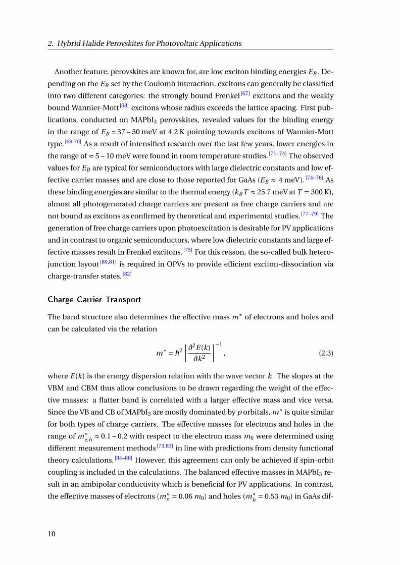
The band structure also determines the effective mass m∗ of electrons and holes and
can be calculated via the relation
m∗ =ħ2[∂2E(k)
∂k2
]−1
, (2.3)
where E(k) is the energy dispersion relation with the wave vector k. The slopes at the
VBM and CBM thus allow conclusions to be drawn regarding the weight of the effec-
tive masses: a flatter band is correlated with a larger effective mass and vice versa.
Since the VB and CB of MAPbI3 are mostly dominated by p orbitals, m∗ is quite similar
for both types of charge carriers. The effective masses for electrons and holes in the
range of m∗e,h ≈ 0.1 – 0.2 with respect to the electron mass m0 were determined using
different measurement methods [73,83] in line with predictions from density functional
theory calculations. [84–86] However, this agreement can only be achieved if spin-orbit
coupling is included in the calculations. The balanced effective masses in MAPbI3 re-
sult in an ambipolar conductivity which is beneficial for PV applications. In contrast,
the effective masses of electrons (m∗e = 0.06 m0) and holes (m∗
h = 0.53 m0) in GaAs dif-
10

2.2. Optoelectronic Properties
fer significantly because the band bending is different in the VB and CB as it is a p-s
type semiconductor (see Figure 2.2b). [63,87]
The most important parameter regarding charge transport is the charge carrier mo-
bility µ. Several techniques have been employed to determine µ in lead halide per-
ovskites which led to a wide range of reported values. Photoluminescence quench-
ing (PLQ) measurements revealed mobilities in the range of µ≈ 1 cm2/(Vs) for both
electrons and holes in MAPbI3. [88,89] Other contactless measurement methods, such as
time-resolved microwave conductivity (TRMC) or time-resolved terahertz spectroscopy
(TRTS), where usually the sum Σµ of electron and hole mobilities is being probed, re-
vealed values in the range of 20 – 70 cm2/(Vs). [90–93] Even higher mobilities of more
than 100 cm2/(Vs) have been measured on single crystals using electrical measure-
ment methods, like time-of-flight (TOF) or space charge limited current (SCLC). [94,95]
This large range of reported values might be partially explained by different sample
qualities and preparation methods of the studied perovskite films, but can also be at-
tributed to the applied measurement techniques as the excitation intensities of steady-
state and pulsed methods can vary significantly. [96] Furthermore, it is of importance
whether the mobility is investigated locally within a crystal domain or long-range trans-
port properties are measured. For example, the influence of grain boundaries on charge
carrier transport is still being discussed and is not yet fully understood. [97,98] A recent
study by Lim et al. has determined long-range charge carrier mobilities of 2 cm2/(Vs)
for polycrystalline MAPbI3 films, which is lower compared to the already discussed val-
ues and indicates that these large mobilities describe short-range transport proper-
ties. [99] Although the mobilities for low temperature solution-processed materials (see
Section 4.2) are considered to be high, they are rather small compared to other inor-
ganic semiconductors such as Si or GaAs, where the electron mobility is in the range
of 1500 – 8000 cm2/(Vs). [87,100] In the simple drude picture, µ of a conductor depends
only on m∗, the average scattering time of a charge carrier τscat and the elementary
charge q of a charge carrier via the relation [101]
µ= q ·τscat
m∗ . (2.4)
Considering the similar values for the effective masses in perovskites and Si/GaAs, the
low mobilities of MAPbI3 have to result from a large variation of τscat and therefore
different electron-phonon coupling. In principle, temperature-dependent measure-
ments can reveal the nature of mobility limitations caused by scattering. Several stud-
ies found a power law of µ ∝ T −1.5 leading to the conclusion that elastic scattering
with acoustic phonons is the main limiting factor in the room temperature tetrag-
onal phase. [91,102,103] In some cases even stronger temperature dependencies are re-
11

2. Hybrid Halide Perovskites for Photovoltaic Applications
ported. [104,105] In contrast, calculations have demonstrated that the coupling to acous-
tic phonons is rather weak and would limit the mobility to a few thousand cm2/(Vs). [106,107]
Recent studies concluded both experimentally [108] and theoretically [109] that scatter-
ing with longitudinal optical phonons associtated with Fröhlich coupling is dominant
at room temperature limiting the maximum achievable mobility to 30 – 80 cm2/(Vs),
which is in agreement with experimental results. [110] The theory of enhanced Fröhlich
interactions is supported by the polar nature of Pb-I bond in MAPbI3. [111] In line with
this picture, Zheng et al. clarified that the formation of large polarons also plays an im-
portant role for charge carrier transport and decreases µ by a factor of two. [112] How-
ever, the temperature dependence of this scattering theory does not match with experi-
mental results and is thus still under debate since scattering with polar optical phonons
scales theoretically with µ∝ T −0.5. [104,113] Since the temperature dependence of mo-
bility is typically ruled by a superimposition of different scattering processes, it is also
suggested that non-conventional models should be used for the description of carrier
charge transport in lead halide perovskites. [113,114]
Furthermore, the mobility as well as the charge carrier lifetime τ determine the dif-
fusion length LD which is defined as [115]
LD =√
kB T
qµτ. (2.5)
Here, T is the temperature and kB the Boltzmann constant. Considerations on charge
carrier recombination and its impact on τ will be provided in Chapter 3. LD speci-
fies the mean free path length between the generation and recombination of a charge
carrier in a semiconductor and is an important parameter, as it defines the optimal
layer thickness of a solar cell. It is also considered to be a quality factor of a material
since it comprises both the transport and recombination properties. The chronologi-
cal evolution of the experimentally determined diffusion lengths for MAPbI3 is shown
in Figure 2.3, where the data is visualized with different colors depending on whether
the value was determined on a film (blue) or a crystal (green). The diffusion length of
a few nanometers in 2009 was increased by several orders of magnitude within a few
years and now amounts to several hundred micrometers determined on single crys-
tals. [95,116] Intensive optimization of the preparation and deposition methods of per-
ovskites has allowed even polycrystalline films to have long diffusion lengths in the
range of ≈ 10 µm and thus being close to single crystal quality. [92,117] Since state-of-
the-art perovskite solar cells typically only have thin active layers of a few hundred
nanometers, the high diffusion lengths allow for efficient charge carrier extraction.
12

2.2. Optoelectronic Properties
0.001
0.01
0.1
1
10
100
1000
diffu
sion
leng
th [µ
m]
201920172015201320112009
time [year]
crystal film
Figure 2.3.: Evolution of measured LD values for MAPbI3 in the last decade. Through pro-cess optimization, the diffusion length of the charge carriers in films (blue points)could be increased by several orders of magnitude. In addition, values determinedon crystals (green points) are presented to show that the polycrystalline films areof almost single crystalline quality. Values are collected from the following Refer-ences [17,88,89,92,95,115–120].
So far, mostly MAPbI3 as the most representative absorber was discussed in this
section. However, the exchange of individual ions can have a significant influence
on the optoelectronic properties. Depending on the chemical composition, the band
gap can be continuously tuned over a wide range. By replacing or intermixing I− with
Br− or Cl−, the band gap is increased to 2.33 eV for pure methylammonium lead bro-
mide (MAPbBr3) and 3.12 eV for methylammonium lead chloride (MAPbCl3). [121,122]
Other works have successfully substituted the A-site cation by Cs+ (cesium lead iodide,
CsPbI3: Eg = 1.73 eV) or FA+ (formamidinium lead iodide, FAPbI3: Eg = 1.48 eV). [123,124]
Band gap tuning also has been exploited by replacing the Pb2+ cation with other met-
als like tin where methylammonium tin iodide (MASnI3) leads to Eg = 1.30 eV. Interest-
ingly, the band gap does not follow a linear trend if Sn2+ is mixed with Pb2+ and Eg
decreases even further to 1.17 eV for both MASn0.75Pb0.25I3 and MASn0.50Pb0.50I3 com-
pounds as reported by Hao and coworkers. [125] This variability has allowed perovskites
to be employed not only in single-junction devices, but also in a multi-junction con-
figuration in tandem solar cells [126,127] and other applications. For example, exten-
sive research efforts are also focused on the implementation in photodetectors, [128,129]
light-emitting diodes (LEDs), [130,131] lasers [132,133] or scintillators [134] for the detection
of ionizing radiation. [135] Due to their optoelectronic properties and versatility, lead
halide perovskites thus represent a new class of interesting organic-inorganic semi-
conductors offering a wide range of possible applications.
13

2. Hybrid Halide Perovskites for Photovoltaic Applications
2.3. Perovskite Photovoltaics
This section describes the working principle of perovskites solar cells and gives a short
introduction to the variability of possible device layouts. Further, the current-voltage
characteristic is explained and the most important PV parameters like the PCE are in-
troduced. In the end, the so-called current-voltage hysteresis, often observed in per-
ovskite solar cells, will be discussed.
2.3.1. Device Layout and Working Principle
Perovskite Solar Cell Architectures
The scientific interest in solar cells based on metal halide perovskite materials during
the last decade led to a multitude of different device architectures. Kojima et al. imple-
mented both MAPbI3 and MAPbBr3 in DSSCs, where the thin perovskite layer replaced
a dye. [17] These electrochemical cells typically employ a µm-thick mesoporous TiO2
layer on which the dye/perovskite layer is deposited. The photogenerated electron-
hole pair is separated and the electron is transferred to the titanium dioxide lattice and
further to an electrode. The mesoporous structure complicates the contact between
the dye and a hole extraction layer, which is necessary to transport the positive charge
to the counter electrode. To overcome this issue, a liquid electrolyte is used, allowing
for a full penetration of the TiO2/dye network. The first perovskite solar cell used the
redox pair I2/I− as an electrolyte. In this system, the I− ions get oxidized to elementary
iodine by transferring an electron to the perovskite layer. Then, it gets reduced again
at the counter electrode to close the electrical circuit. The energy of electrons in the
valence band of the perovskite has therefore to match the oxidation potentials of the
halides in the electrolyte. In contrast, excited electrons from the perovskite cannot flow
to the liquid electrolyte since no states at the corresponding energies are available.
It took 3 years for the perovskite to re-enter the PV stage with a more than twofold in-
crease in efficiency from 3.8 % to around 10 %. [19] This was realized by introducing the
solid-state hole transport layer (HTL) 2,2,7,7–tetrakis(N,N–p–dimethoxy–phenylamine)–
9,9–spirobifluorene (spiro-MeOTAD) to replace the liquid electrolyte which also im-
proved the device stability significantly. The concept of a so-called solid-state DSSC
was already introduced in the 90s by Tennakone, [136] Murakoshi [137] and Bach. [138] A
milestone in the development of perovskite PVs was the replacement of n-type TiO2
with insulating aluminium oxide (Al2O3) which increased the PCE even further. [18] Two
important conclusions were drawn from this work: first, it became apparent that an
additional capping layer of perovskite on top of mesoporous TiO2 does not limit the ef-
14

2.3. Perovskite Photovoltaics
ficiency, which clearly distinguishes the structure from a regular DSSC. Second, charge
transfer to TiO2 was not needed since the transport of electrons in the perovskite was
faster than in mesoporous titanium dioxide, which was interpreted as a clear indication
of amibipolar transport. These publications are considered as pioneering works guid-
ing further research on perovskites and paved the way for the layouts currently in use.
Figure 2.4a depicts the architecture just described, which is one of the most frequently
employed designs for perovskite solar cells. A glass substrate is initially coated with the
electrode, a transparent conductive oxide that must be light-transmitting since the fi-
nal solar cell is illuminated from the glass side. In case of the mesoporous architecture,
fluorine-doped tin oxide (FTO) is preferred because it resists the necessary sintering of
the mesoporous TiO2 layer at 400 – 500 °C. Electron transport in porous TiO2 is usually
limited by trapping and detrapping in sub-band gap states [139] and leads therefore to
low mobilities of around 10−2 cm2/(Vs), [140] which explains the faster transport in the
perovskite film observed by Lee et al. when TiO2 is replaced by insulating Al2O3. [18] In
the past years, a number of other mesostructures were also implemented as electron
transport layers (ETL) such as zinc oxide (ZnO), [141] zirconium dioxide (ZrO2) [142] or
tin dioxide (SnO2). [143] The porous network is then infiltrated by the perovskite with a
closed capping layer. An HTL in combination with an electrode completes the solar
cell. Among the HTM’s, spiro-MeOTAD is the most commonly chosen material, al-
though a variety of other compounds can also be used. [144] Gold, silver or other metals
are then applied as the electrode.
The ambipolar transport and the high carrier diffusion lengths (see Section 2.2) also
allow the mesoporous network to be substituted by a planar transport layer as illus-
transparent conductive oxideglass substrate
V
perovskite
transport layer
metal
mesoporous scaffold
metal
transport layer
transport layer
perovskite
transparent conductive oxideglass substrate
V
(a) mesoporous device layout (b) planar device layout
Figure 2.4.: Device architectures for perovskite solar cells. In (a), a mesoporous scaffoldis used as a transport layer, while a planar configuration is shown in (b). The glasssubstrate is coated with a transparent conductive oxide acting as an electrode andfollowed by a transport layer, which can be either planar or mesoporous. The activelayer with the perovskite and another transport layer are located above. Finally, ametal electrode completes the solar cell.
15

2. Hybrid Halide Perovskites for Photovoltaic Applications
trated in Figure 2.4b. Here, the perovskite is embedded between the HTL and ETL re-
sulting in a p-i-n or n-i-p configuration. Instead of FTO, indium-doped tin oxide (ITO)
is often implemented as an transparent conductive oxide. Various transport materi-
als have been established in the meantime, whereby poly(3,4–ethylenedioxythiophe-
ne):poly(styrenesulfonate) (PEDOT:PSS) [145] and poly–(bis(4–phenyl)(2,4,6–trimethyl-
phenyl)amine) (PTAA) [146] are the most prominent representatives of the HTLs and the
C60[145,147] fullerene or [6,6]-phenyl-C-61-butyric acid methyl ester (PC61CM) [148,149]
are frequently used as ETLs. Often a sequence of several transport layers [146,150] is com-
bined or dopants [151,152] are added to increase the conductivity and improve charge
carrier extraction. The great potential of this design, which is similar to those of or-
ganic solar cells, was demonstrated by Liu et al. in 2013, when PCEs of over 15 %
were achieved. [153] The planar device architecture exhibits several advantages over the
mesoporous design such as simplified fabrication and usually reduced hysteresis dur-
ing current-voltage measurements as discussed in more detail in Section 2.3.2. Never-
theless, PCEs of over 20 % can be achieved regardless of layout. [154]
Operating Principle
The working principle is quite similar in both type of devices and depends strongly on
the optoelectronic properties of the perovskite itself. To generate electricity, a number
of different steps are necessary as summarized in Figure 2.5. In the very first step, an
incident photon is absorbed. According to the photovoltaic effect, [155,156] which de-
scribes the interaction of light with matter, an electron is lifted from the valence band
to a higher energetic state in the conduction band of the semiconductor (i). If the en-
ergy of the photon is not sufficient, no absorption can occur, while charge carriers with
excess kinetic energy are created if the energy is higher than Eg (ii). For MAPbI3, it
has been shown that the cooling of these so-called hot-carriers (due to a larger effec-
tive temperature compared to the temperature of the crystal lattice) is regulated by the
emission of longitudinal optical phonons, providing lifetimes in the range of 1 – 100 ps
which is longer compared to conventional semiconductors. [157,158] The slow thermal-
ization processes are attributed to a hot-phonon bottleneck caused by an increased
phonon reabsorption in the presence of a non-equilibrium phonon population at high
carrier densities. [74,159] Irrespective of whether charge carriers were generated accord-
ing to (i) or (ii), they are initially present as excitons, which is indicated in step (iii). As
already described in Section 2.2, these are weakly bound Wannier-Mott excitons which
get separated on the ps time scale. [160] The fact that hot charge carriers are present as
free carriers qualifies lead halide perovskites as candidates for hot carrier solar cells,
where excited charge carriers with excess energy get separated and extracted before
16

2.3. Perovskite Photovoltaics
-+
-
+
-
+
(iii) (iv)
(v)
(v)
anode
cathodeperovskite
-
+(ii)(i)
-
+
CB CB
VBVB phonon
absorption separation and transport
ħEg ħEgphonon
Figure 2.5.: Schematic depiction of the working mechanism of a perovskite solar cell. Pho-tons with the energy of the band gap (i) or with a higher energy (ii) are absorbed andgenerate a weekly bound exciton. After the separation of the electron hole pair (iii)both types of charge carriers diffuse to the respective contacts (iv) and get extracted(v). Further details are given in the text. For clarity, charge carrier recombination isneglected and will be discussed in Chapter 3.
they relax to the VBM and CBM, respectively. [161,162] After the carriers are separated and
a splitting of the electron and hole quasi Fermi levels EF n and EF p is established, they
must move to separate electrodes. For this reason, every solar cell requires a build-in
asymmetry that ensures that charge carriers with different polarities can be collected
and extracted independently at individual contacts (steps (iv) and (v)). Accordingly,
the transport layers and contacts are of central importance for the working principle
of perovskite solar cells and a prerequisite to obtain a diode structure. Usually a good
transport layer is characterized by a selectivity to only one carrier type. This can, for ex-
ample, be achieved by energy level alignment, allowing one kind of carriers to enter the
layer and blocking the opposite charge carriers due to a lack of free energetic states. [163]
Würfel et al. also demonstrated that a difference in electron and hole conductivities
in two regions of a device already can be sufficient to obtain charge carrier separa-
tion. [164] When the HTL and ETL get in contact with the perovskite, the Fermi level EF
equilibrates over the whole device and the difference of work functions of the trans-
port layers results in a build-in voltage Vbi . Depending on the solar cell technology, Vbi
can be present over the whole absorber width or narrowed down to a thin space charge
region. The role of Vbi is intensively discussed in literature, since its strength and the
length over which it extends has a direct influence on charge carrier separation mech-
anism both in the dark and under illumination. [165,166] The interplay of the build-in
voltage, charge carrier drift and charge carrier diffusion was very recently investigated
by the group of Nazeerudin. [167] The authors varied Vbi by shifting the work function
of the ETL by about 1 eV and observed very similar Voc ’s, indicating that the build-in
electrical field plays a minor role in the operation mechanism. The open-circuit volt-
age is therefore controlled by charge carrier recombination and the quasi Fermi levels
17

2. Hybrid Halide Perovskites for Photovoltaic Applications
in the perovskite with the transport layers following the respective levels. As a direct
consequence, a flat band structure is assumed to exist in the perovskite and carrier
transport should be ruled by diffusion and not by drift due to electrical fields. [167,168]
This result is also supported by cross sectional Kelvin probe force microscopy mea-
surements, which revealed a field-free MAPbI3 layer embedded in a device configura-
tion under both short- and open-circuit conditions. [169] The observed field-screening
is attributed to the rearrangement of mobile ions in the perovskite film, which will be
further addressed in Section 2.3.3. In line with previous statements, calculations [165]
have demonstrated that PV devices benefit from diffusion dominated transport if the
diffusion length is higher than the active layer thickness which is indeed the case for
most lead halide perovskite solar cells (see Section 2.2). Nevertheless, the exact work-
ing principle of perovskite solar cells still remains topic of ongoing research and more
experimental work is necessary since a better understanding would help to boost the
PCE even further.
2.3.2. Current-Voltage Characterization and Photovoltaic
Performance
The main characterization of PV devices is realized by measuring the current depen-
dence on a externally applied voltage, which is usually referred to as the current-voltage
( j -V ) response. In order to compare different solar cells with each other, standard illu-
mination conditions have been introduced. The AM1.5 G spectrum with an irradiance
of 100 mW/cm² is often termed “1 sun” illumination and defines the incident power PL
the solar cell is illuminated with. The spectral distribution is set by the global (G) stan-
dard reference spectrum (average of direct and diffuse solar irradiance) passing the air
mass (AM) under the solar zenith angle of cos(1/1.5) = 48.19°. [170] The j -V characteris-
tics normalized to the active area of a typical perovskite solar cell both in the dark and
under 1 sun illumination are summarized in Figure 2.6a in a linear and in Figure 2.6b
in a semi-logarithmic representation. Several points of interest are highlighted for the
illuminated curve, namely the the short-circuit current density ( jsc ), the open-circuit
voltage (Voc ) and the maximum power point (MPP). When both contacts are connected
through an external circuit and no voltage is applied, the resulting current is called jsc ,
where the corresponding band diagram is depicted in Figure 2.6c. In this scenario, the
Fermi level is equilibrated over the whole device and the photogenerated charge carri-
ers get extracted at the respective contacts. As discussed already in the previous Sec-
tion 2.3.1, charge transport can occur via both drift or diffusion, depending on Vbi . For
clarity, mobile ions (see Section 2.3.3) and doping are not considered in Figure 2.6c. In
18

2.3. Perovskite Photovoltaics
-20
-10
0
10
20cu
rren
t den
sity
[mA
/cm
²]
1.00.80.60.40.20.0-0.2
voltage [V]
8
6
4
2
0
power density [m
W/cm
²]
dark illuminated power density
jsc
Voc
MPP
10-5
10-4
10-3
10-2
10-1
100
101
102
curr
ent d
ensi
ty [m
A/c
m²]
1.21.00.80.60.40.20.0-0.2
voltage [V]
dark illuminated fit
Rseries
limited
Rshunt
limited exp. regime
(a) (b)
-
Short-circuit conditions:
perovskite
HTL
EFn
EFp
ETL
++
--
EF
perovskite
+
-
+
Open-circuit conditions:
perovskite
perovskite HTL
EFn
EFp
ETL
qVoc
+ + + + + +
- - - - - -
(c) (d)
Figure 2.6.: (a) Current-voltage characteristics in the dark and under simulated AM1.5 G il-lumination (left axis) and the power density (right axis) of a perovskite solar cell. Themaximum power point indicates the part of the j -V curve where the power densityhas its maximum (green dashed line). The fill factor is defined by the maximumpower point and corresponds to the ratio of the maximum power density and theproduct jsc ·Voc . (b) Semi-logarithmic representation of both j -V curves includinga fit according to Equation 2.8. In addition, band diagrams of a solar cell are shownunder (c) short-circuit and (d) open-circuit conditions. [163,166] At short-circuit, thephotogenerated charge carriers are extracted, whereas at open-circuit conditions,the generation rate equals the recombination rate and the resulting quasi Fermi levelsplitting creates Voc .
contrast to short-circuit, current flow is suppressed and no charge carriers get extracted
under open-circuit conditions when the quasi Fermi level splitting (EF n and EF p ) due
to photogenerated charge carriers is fully compensated by an externally applied bias,
the Voc (Figure 2.6d). Under these conditions, both the VB and the CB are aligned flat
and the recombination rate balances the photogeneration rate. This point is therefore
of particular interest for investigating recombination losses in PV devices and will be
19

2. Hybrid Halide Perovskites for Photovoltaic Applications
addressed in this thesis. Increasing the voltage further to values above Voc leads to an
injection of charge carriers, which recombine inside the device. Another feature of the
illuminated j -V response is the MPP, located at the voltage where the power density
j (V ) ·V (Figure 2.6a, green line) has its maximum (Pmax). The MPP determines the fill
factor FF, which is defined as
F F = Pmax
jsc ·Voc= jMPP ·VMPP
jsc ·Voc(2.6)
and can be understood as the ratio between the theoretically possible power ( jsc ·Voc )
and the maximum power output of the device which is illustrated by the two grey
squares in Figure 2.6a. Thus, it describes the "squareness" of the j -V curve. With the
above-mentioned PV parameters, the PCE of a solar cell can be written as
PC E = Pmax
PL= jsc ·Voc ·F F
PL. (2.7)
Highly efficient solar cells therefore require that jsc , Voc and FF are optimized at the
same time. To obtain the maximum power, an external load must be adjusted such
that the solar cell is at the MPP under illumination.
In general, the relation between current and voltage of a solar cell can be described
by the generalized Shockley equation [171]
j (V ) = j0
[exp
(e(V − j Rser i es)
ni d kB T
)−1
]+ V − j Rser i es
Rshunt− jph , (2.8)
where j0 is the dark saturation current density, ni d is the diode ideality factor, Rser i es
is the series resistance, Rshunt is the shunt resistance and jph is the photocurrent den-
sity. The impact of these parameters is demonstrated in Figure 2.6b by fitting the j -V
response in the dark ( jph = 0) with Equation 2.8 (red dashed line). The exponential
diode behavior of the device is controlled by the combination of the material proper-
ties j0 and ni d . Recently, Cuevas pointed out that a more suited expression for j0 is
"thermal equilibrium recombination current" since it corresponds to the recombina-
tion of charge carriers generated by the thermal background radiation. [172] In case of
ideal diodes (ni d = 1), j0 contains all information about charge carrier recombination.
However, in many cases ni d deviates from unity and is therefore also used as an ad-
ditional parameter describing the dominant recombination processes in solar cells as
discussed in Section 3.3. [173,174] The divergence of the exponential behavior is a conse-
quence of resistive losses induced by Rser i es and Rshunt . Resistances inside the device
and from the electrical circuit are included in Rser i es , which can negatively influence
the FF. The impact of the series resistance can be observed for high voltages in Fig-
20

2.3. Perovskite Photovoltaics
ure 2.6b. Rshunt accounts for leakage currents inside the device, for example caused
by pinholes and affects the diode current at low voltages. In case of low Rshunt , it is
even possible that the open-circuit voltage is reduced. High parallel resistances and
low series resistances should therefore always be aimed for.
Bucket Analogy
To illustrate the introduced PV parameters, a solar cell is compared with a bucket in the
following. The comparison between a bucket and a solar cell is based on lectures from
Yablonovitch and was recently adopted by a book [175] from Green and co-workers. A
modified version is shown in Figure 2.7 to demonstrate the different states in which the
solar cell is operating under jsc , MPP and Voc conditions. A PV device is symbolized by
an empty bucket, which gets filled with water drops representing excited charge carri-
ers in the active layer. At the bottom, a valve controls the water flow and therefore also
the water level and pressure inside the bucket. Both, water flow and water level corre-
spond to the current and the voltage of the solar cell. The water flow drives a wheel,
where the dissipated power depends on the product of flow and pressure. This is the
analogy to the power generated by a PV device. Thus, the valve controls the rotational
speed of the wheel and determines the current state of the bucket. In the solar cell pic-
ture, it corresponds to the resistance of the load which is connected to the device. In the
band
gap
(i) short-circuit conditions: (iii) open-circuit conditions:(ii) maximum power point:
jscjmpp
Vm
pp Voc
Figure 2.7.: Bucket analogy of the working principle of a solar cell. The bucket represents aPV device where the height corresponds to the band gap of the active layer. A waterwheel has its equivalence in the power output of a solar cell. When it rains, the waterdrips into the bucket and the position of the valve determines the condition thatsets inside. Under (i) short-circuit, the valve is fully open, all the water flows out andthe water level, which corresponds to the voltage, is close to zero. At (ii) MPP, thevalve is set so that the product of water level and water flow (current in a device)is maximized and the wheel turns at the highest rotational speed. In contrast, thevalve is completely closed under (iii) open-circuit and the resulting water level isequivalent to Voc . [175]
21

2. Hybrid Halide Perovskites for Photovoltaic Applications
case of an open valve, the collected water drops out of the bucket, preventing the wa-
ter level from increasing. Since no pressure can build up, the wheel does not turn and
no power is generated. This situation corresponds to a solar cell under (i) short-circuit
conditions. The power output can by increased by closing the valve continuously un-
til it reaches the MPP. At this point, the water level and water flow are optimized such
that wheel rotates with the maximal rotational speed, which is equivalent to a solar
cell operating at its (ii) MPP. If the valve is further closed, the wheel gets slower again
and the dissipated power decreases towards zero in the case of a closed bucket. This
state corresponds to (iii) open-circuit conditions, where the maximum water height is
reached and the solar cell provides the Voc . However, under these conditions, the water
level would increase until it finally spills over which cannot be observed in real devices
since the Voc is always smaller than Eg . Therefore, additional loss processes, the re-
combination of charge carriers, must be considered and will be discussed in Chapter
3.
2.3.3. Hysteresis Eects
One of the most controversial phenomena in perovskite solar cells is the so-called hys-
teresis. It describes slow, time-dependent processes that usually occur in electrical
measurements. During current-voltage characterization, the direction of the measure-
ment, i.e. whether the voltage is swept from negative to positive (forward) or vice versa
(backwards), can have a large influence on the resulting current. Figure 2.8 shows
two sets of j -V curves in the dark and under illumination, where the degree of hys-
teresis differs significantly and complicates the determination of PCE. The scan rate
was 0.5 V/s such that the entire measurement was performed on a time scale of sec-
onds. Both devices show a higher performance when the current response is mea-
sured from positive to negative voltages. The difference between the studied devices
are the transport layers surrounding the MAPbI3 film. In case of Figure 2.8a, a p-i-n
architecture is used with PEDOT:PSS as the HTL and a combination of PC61BM and
C60 as ETL’s. In Figure 2.8b, the perovskite is sandwiched between planar TiO2 and
poly(3-hexylthiophene-2,5-diyl) (P3HT) leading to a n-i-p layout. Obviously, the im-
plemented transport materials and the structure of the device strongly influence the
gap between the forward and backward scans in line with other reports. [176–183] The
composition of the perovskite also determines the extent of hysteresis, where the in-
corporation of FA+, Cs+, Rb+ and K+ as the A-position cations having a diminishing
effect. [184–186] However, it is not only the materials involved that play a role, but also
the conditions under which the solar cell is being measured. Numerous publications
have shown that the bias prior to a j -V loop, [180,187,188] the applied voltage range [189]
22

2.3. Perovskite Photovoltaics
-15
-10
-5
0
5cu
rren
t den
sity
[mA
/cm
²]
1.00.80.60.40.20.0
voltage [V]
/ dark/ illuminated
PEDOT:PSS / MAPbI3 / PC61BM / C60
PCE = 7.0 %
PCE = 7.8 %-15
-10
-5
0
5
curr
ent d
ensi
ty [m
A/c
m²]
1.00.80.60.40.20.0
voltage [V]
TiO2 / MAPbI3 / P3HT
/ dark/ illuminated
PCE = 1.6 %
PCE = 7.4 %
(a) (b)
Figure 2.8.: Examples of j -V characteristics from MAPbI3 solar cells with hysteresis. Whena voltage is applied, the measured current in the dark and under 1 sun illuminationdepends on the direction of the voltage sweep which complicates the PCE determi-nation. The device in (a) uses PEDOT:PSS as a HTL and a combination of PC61BMand C60 as ETL’s and corresponds therefore to a p-i-n layout. In contrast, the curvesin panel (b) are determined on a n-i-p solar cell, where a compact TiO2 layer actsas the ETL and P3HT as the HTL. In both cases, ITO and gold are employed as elec-trodes and the scan rate was set to be 0.5 V/s.
and the scan rate [187,190] are also important. The anomalous behavior can also be af-
fected by light soaking [191,192] and temperature. [193,194]
In principle, hysteresis during j -V characterization is a property common to all types
of solar cells. For example, silicon PVs or DSSCs also reveal differences between for-
ward and backward sweeps at sufficiently high scanning speeds. [195,196] This is ascribed
to capacitive effects in the device, where charge carriers cannot follow the voltage cy-
cling. In the simplest case, the solar cell acts as a plate capacitor and gets charged dur-
ing the forward scan and discharged during the backward scan. Additional contribu-
tions to hysteresis may be caused by trapping and release of charge carriers, when the
release rate of traps is slower compared to the scan velocity. However, these effects only
become visible during short measurement times in the millisecond range, which is in
clear contradiction to perovskite solar cells. Here, the hysteresis is more pronounced
and sometimes still present at very slow scan rates. [187] It has been even shown that
the PL intensity measured on films or the Voc and PCE of full devices can build up to
several hundred of seconds. [182,190,197] Consequently, additional effects must be taken
into account to explain the observed anomalies.
23
2. Hybrid Halide Perovskites for Photovoltaic Applications
Ferreoelectricity
The physical origin of the hysteresis effect has been debated for a long time and vari-
ous explanations have been proposed. Initially, polarization of the perovskite was sug-
gested to be responsible for hysteresis, because a large variety of ABX3 compounds is
known for its polarizability which causes, for example, ferroelectric behaviour. How-
ever, there are a several conflicting works on the presence of ferroelectricity. Theoret-
ical studies opened up the possibility that lead halide perovskites show spontaneous
electric polarization in the tetragonal phase. Different origins have been suggested like
oriental polarization from the MA+ dipole or ionic polarization induced whether by
a displacement between MA+ and the lead iodide sublattice or a shift of Pb2+ within
the PbI64 – octahedral. [198–200] Out of these possible contributions, the largest part is
attributed to the asymmetric organic cation. [198,200] In line with these reports, Pecchia
et al. proposed ferroelectric order in MAPbI3 at length scales of 8 – 10 nm where elec-
trons and holes can accumulate separately. [201] In contrast, it is also calculated that the
ferroelectric behaviour is not stable at room temperature and can only be observed for
temperatures below 50 K. [202] Additionally, experimental works spread further confu-
sion within the scientific community as contradictory results on the question, if lead
halide perovskites are [203–206] of ferroelectric nature or not, [207,208] exist. It is postu-
lated that dipoles in the perovskite would result in an internal electrical field which can
strengthen or weaken an externally applied field leading to the observed differences in
scan directions during j -V characterization. [180,209] However, this theory seems un-
likely to be the main origin of hysteresis since the timescale of switching domains are
reported to be in the range of ~ 0.1 – 1 ms and thus intrinsically too fast compared to
the observed effects on the timescale of seconds (see Figure 2.8). [210] It is also demon-
strated, that the rotations of the organic cation do not influence photogenerated charge
carriers at all. [62]
Trapping and Detrapping of Charge Carriers
Further speculations exist, that charge trapping and detrapping processes may be in-
volved in hysteresis during j -V measurements. [211] Trap states are associated with de-
fects in the crystal lattice that are able to trap electrons or holes. These processes can
occur in the bulk of the perovskite and at the interfaces to the transport layers. It is
suggested that photogenerated charge carriers are trapped when a forward bias is ap-
plied and then released again when the voltage is set to zero again during a measure-
ment. This mechanism can then result in differences between the forward and back-
ward scans. [212] The theory is supported by different works where passivating layers are
24
2.3. Perovskite Photovoltaics
implemented in devices to reduce the amount of traps states leading to a decreased
hysteresis. For example, the group of Snaith passivated the surface of TiO2 with the
fullerene C60 resulting in an increased PCE and a reduced current-voltage discrepancy
between both scan directions. [213] Similarly, Shao et al. deposited PC61BM on top of
a perovskite layer and measured that the amount of surface trap states is reduced by
more than two orders of magnitude, again decreasing the hysteresis significantly. [176]
This theory therefore supports the large influence of the transport layers on the emer-
gence of hysteresis. However, since the presence of trap states is not a property that
is exclusively encountered in perovskite solar cells, there must be further explanations
for j -V hysteresis.
Mobile Ions
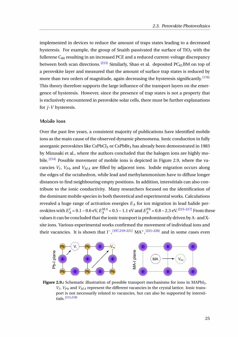
Over the past few years, a consistent majority of publications have identified mobile
ions as the main cause of the observed dynamic phenomena. Ionic conduction in fully
anorganic perovskites like CsPbCl3 or CsPbBr3 has already been demonstrated in 1983
by Mizusaki et al., where the authors concluded that the halogen ions are highly mo-
bile. [214] Possible movement of mobile ions is depicted in Figure 2.9, where the va-
cancies VI , VPb and VM A are filled by adjacent ions. Iodide migration occurs along
the edges of the octahedron, while lead and methylammonium have to diffuse longer
distances to find neighbouring empty positions. In addition, interstitials can also con-
tribute to the ionic conductivity. Many researchers focused on the identification of
the dominant mobile species in both theoretical and experimental works. Calculations
revealed a huge range of activation energies E A for ion migration in lead halide per-
ovskites with E IA = 0.1 – 0.6 eV, E M A
A = 0.5 – 1.1 eV and E PbA = 0.8 – 2.3 eV. [215–217] From these
values it can be concluded that the ionic transport is predominantly driven by A- and X-
site ions. Various experimental works confirmed the movement of individual ions and
their vacancies. It is shown that I−, [197,219–221] MA+, [221–226] and in some cases even
Pb
Pb-
I pla
ne
MA
-I p
lane
Pb
Pb Pb
Pb VPb
Pb
I
I
I
I
I
I
VI I
I I
I I
I
MA VMA
Figure 2.9.: Schematic illustration of possible transport mechanisms for ions in MAPbI3.VI , VPb and VM A represent the different vacancies in the crystal lattice. Ionic trans-port is not necessarily related to vacancies, but can also be supported by intersti-tials. [215,218]
25

2. Hybrid Halide Perovskites for Photovoltaic Applications
Pb2+ [222,227] ions are moving in the crystal lattice under electrical fields. Further, the
diffusion coefficients have been determined to be in the range of 10−9 cm2/s for iodide
and 10−12 cm2/s for methylammonium. However, the concentration of MA+ ions is
one order of magnitude higher compared to mobile I− ions. [221] Senocrate et al. con-
cluded that the experimentally observed ionic conductivity in MAPbI3 is higher than it
is calculated in the case of pure MA+ movement pointing towards iodide-driven hys-
teresis effects. [226] The effect of illumination on the ionic conductivity has also been
investigated leading to the conclusion that light generates additional iodine vacancies
in the perovskite. [228] Very recently, Meggiolaro et al. tried to obtain a more compre-
hensive picture of mobile ions and they linked the variation of measured activation
energies and diffusion parameters to the polycrystallinity of perovskite films where the
surfaces dominate ion migration behavior. [229] This is in line with reports, where grains
boundaries have been identified as the main transport pathways for ions. [230]
The extact mechanism how mobile ions influence electrical measurements like j -V
characterization is still under debate. Figure 2.10 illustrates the ion distribution and
its impact on band alignment at both short-circuit and open-circuit conditions under
equilibrium. For clarity, only methylammonium and iodide ions/vacancies (MA+, I−,
V−M A and V+
I ) are included in the scheme since these are believed to contribute most
to hysteresis effects like discussed before. Under jsc conditions (Figure 2.10a), mobile
ions move trough the perovskite film according to the build-in electrical field (see Fig-
ure 2.6c). This results in the screening of the built-in potential, which can not further
act as a driving force for the extraction of charge carriers leading to a reduced jsc as
shown in Figure 2.8b. When a forward voltage is applied and the scanning speed is
faster compared to the moving ions, band valleys are generated in the CB and VB forc-
ing excited electrons to accumulate close to the HTL and holes close to the ETL. Both
types of charge carriers are therefore trapped at the wrong electrodes which leads in
case of non-selective contacts to increased charge carrier recombination at the inter-
faces reducing both F F and Voc . [231,232] If the applied voltage approaches and exceeds
Voc , the driving force that separates ions, vanishes. This situation is summarized in
Figure 2.10b, where the ions are uniformly redistributed again. In the backward scan,
FF and Voc are increased since the charge carrier transport and recombination are not
negatively affected by an unfavorable ion distribution in the device. It is obvious that
hysteresis effects therefore can be described as a combination of ionic and electronic
charge carrier distributions in the device. The hypothesis of non-selective transport
layers in combination with mobile ions is supported by a large number of transient
experiments, like the slow build-up of open-circuit voltage after switching on the light
26

2.3. Perovskite Photovoltaics
-
perovskite
HTL
ETL
+ +
--
EF
Short-circuit conditions at equilibrium:
perovskite
+
MA+VMA
-+VI
VMA-
I-
I-
+VI
MA+
-
+
perovskite
perovskite HTL
EFn
EFp
ETL
+ + + + + +
- - - - - -
Open-circuit conditions at equilibrium:
+VI
+VI
MA+
MA+
I-
I-
VMA- VMA
-
(a) (b)
Figure 2.10.: Impact of mobile ions on band energetics at (a) short-circuit and (b) open-circuit conditions under equilibrium. [231,232] At jsc conditions, the build-in potentialforces the ions to move close to the interfaces to the transport layerts. This resultsin a screening of the build-in field, where the extracted charge carriers are mostlydriven by diffusion. In contrast, when the device is stabilized under Voc conditions,the ions are redistributed again. Further explanations on how mobile ions can influ-ence current-voltage measurements are provided in the main text.
and drift-diffusion simulations and is therefore widely accepted to be the main cause
of hysteresis. [218,232–237]
During the last years, many researchers focused on the elimination of current-voltage
hysteresis in perovskite solar cells. Various approaches were applied to both the per-
ovskite itself and the surrounding transport layers. To suppress ion movement, Ferdani
et al. substituted the organic cation to increase the activation energy for ion diffusion.
It was demonstrated, that partial replacement of methylammonium by guanidinium in
MAPbI3 suppressed iodide transport. [238] Other attempts optimized the transport lay-
ers and the interfaces to reduce charge carrier recombination and the observable hys-
teresis. [176,179,239,240] To quantify the extend of hysteresis effects, several publications
introduced the hysteresis index H I , [241–244] which quantifies the difference between
the forward and the backward j -V scan. To give an example, according to Li et al., it
can be expressed as follows [244]
H I = PC Eback −PC E f or
PC Eback, (2.9)
where PCE f or and PCEback correspond to the PCE determined from forward and back-
ward scan directions, respectively. A solar cell without hysteresis thus has a H I value
of zero, which increases the larger the difference between forward and reverse direc-
tion gets. However, it is under debate if H I is a useful parameter to describe hysteresis
in perovskite-based devices since it does not account for all relevant conditions like
27

2. Hybrid Halide Perovskites for Photovoltaic Applications
for example the material system or the scan speed. [245] In contrast, it is suggested to
monitor the stability of the important parameters such as jsc , Voc and PCE over time.
For this reason, several authors developed protocols and guidelines for a correct PCE
determination of perovskite solar cells highlighting the importance of stabilized PV pa-
rameters. [246–248]
28

3. Charge Carrier Recombination
in Semiconductors
The following chapter provides insights into loss processes in semiconductors, namely
charge carrier recombination. Carrier recombination dynamics are very relevant for
the functionality of optoelectronic devices. An overview over the most important re-
combination mechanisms will be given, including their impact on the charge carrier
lifetime τ. Finally, it will be highlighted how these recombination mechanisms are con-
nected to PV parameters like Voc in fully working devices.
3.1. Recombination Mechanisms
Recombination of charge carriers is of fundamental importance for semiconductors
in electronic devices like solar cells, LEDs and transistors. In general, all processes
which lead to a depopulation of the excited species are described by recombination
mechanisms and are therefore considered as charge carrier losses. In PV devices, these
carriers cannot consequently get extracted anymore. Thus, in order to increase the
efficiency of a solar cell, every researcher strives for a reduction of unwanted recom-
bination processes. An overview over possible loss mechanisms relevant for the oper-
ation of PVs is provided in Figure 3.1. These processes can be categorized according
to the number of involved particles. Monomolecular or first-order recombination de-
scribes processes with only one particle. This can, for example, be the recombination
of an exciton. As discussed in Section 2.2, photoabsorption yields mostly free charge
carriers instead of excitons. Accordingly, this type of recombination can be neglected
for perovskites, but plays an important role in OPVs. [249] On the other hand, Shockley-
Read-Hall (SRH) recombination is considerably more important for perovskite solar
cells (see (i) in Figure 3.1). In this case, a trap (defect) leads to an energetic state within
the band gap which captures an electron or hole by simultaneous emission of phonons
and mediates therefore a recombination event. Since only one charge carrier is re-
quired for the process, it also represents first-order recombination. At higher charge
carrier concentrations, (see (ii)) band-to-band or second-order (bimolecular) recom-
29

3. Charge Carrier Recombination in Semiconductors
CBM
VBM
-
+
-
+
-
+
photon
-
trap(i) (ii) (iii)
phonon
Figure 3.1.: Overview of different charge carrier recombination mechanisms in semicon-ductors. Trap–assisted recombination is shown in (i), which is induced by energeticstates inside the band gap. This process is usually dominating at low carrier concen-trations, where the density of trap states rules. This mechanism is often describedby Shockley–Read–Hall theory and corresponds to a first-order process. A direct re-combination of an electron in the CB and a hole in the VB with the emission of aphoton is called (ii) band–to–band recombination. Since two particles are involvedin the process, it is often referred to as a second-order process. A three particle lossmechanism is (iii) Auger recombination, where the energy which results from a di-rect electron-hole recombination is transferred to another electron or hole. For allthese processes energy and momentum conservation must be fulfilled.
bination starts to be dominant which involves both an electron in the CB and a hole
in the VB. Here, the recombination event depends on the product of the electron and
hole carrier concentrations n and p, which can be summarized as n2. The recombina-
tion of free charge carriers normally induces the emission of photons, for which reason
these processes are also referred to as radiative recombination. If the excess energy is
directly reabsorbed by a third charge carrier, the process is called Auger recombination
and corresponds to a third-order mechanism scaling with n3. The excited carrier, inde-
pendent if it is an electron or a hole, thermalizes then back to the band edge by emitting
phonons. Just like SRH recombination, this mechanism is also part of non-radiative re-
combination processes and dominates under high charge carrier densities. [250] Since
non-radiative recombination losses lead to the emission of phonons, they increase the
lattice temperature of the solar cell absorber.
Taking all these processes into account, the time-dependent change of charge carrier
density n can be determined by the differential equation
dn
dt=−k1n −k2n2 −k3n3, (3.1)
with k1, k2 and k3 as the respective rate constants of first-, second- and third order
recombination. For simplicity, the generation, diffusion and drift of charge carriers is
neglected in this expression. Since the dominating processes for each rate constant are
known, k1, k2 and k3 can also be substituted by the rate constants kSRH , kr ad and kAug .
30

3.1. Recombination Mechanisms
These processes can be divided into two categories: avoidable and unavoidable charge
carrier recombination as will be further outlined in this chapter.
3.1.1. Shockley-Read-Hall Recombination
Charge carrier recombination via defects is an important loss mechanism in semi-
conductor devices. This type of recombination is usually described within the frame-
work of Shockley-Read-Hall recombination, developed in the middle of the 20th cen-
tury. [251,252] A localized trap can result in an energetic state within the band gap which
can mediate recombination events between electrons and holes from the CB and VB,
respectively. If a trap captures a charge carrier, this carrier can either be released again
by thermal activation or it recombines with a particle of opposite polarity. Therefore,
the time until both carrier types are captured is in competition with the release time of
the trapped carrier and therefore determines the effectiveness of the defect state. Im-
purities, where the time of capturing both charge carriers is shorter than the release
time are called recombination centers. [253] In order to ensure energy conservation,
trapping and detrapping is always related to the emission and absorption of phonons.
The energetic position of the defect state and thus the energy difference to the CB or
VB determines the number of phonons required for capturing a charge carrier. It fol-
lows intuitively that defect states which are located in the middle of the band gap have
the highest probability of mediating a SRH recombination event since energy exchange
with the crystal lattice is less likely when the energetic distance between two states is
large. Hence, a separation into deep traps which act as SRH recombination centers and
shallow traps which are prone to release the captured charge carriers is therefore useful
and frequently used in literature.
According to Shockley-Read-Hall theory, the recombination rate RSRH of photogen-
erated charge carriers via a recombination center with the energy ET can be expressed
using the equation
RSRH = np −n2i
τp (n +nt )+τn(p +pt ), (3.2)
where n and p are the electron and hole concentrations, ni is the equilibrium carrier
concentration of electrons/holes and τn and τp are electron and hole carrier lifetimes.
nt and pt describe the electron and hole densities when the Fermi level equals the
energy of the trap through which the charge carriers recombine and equals
nt = NC exp
(−EC −ET
kB T
)pt = NV exp
(−ET −EV
kB T
) (3.3)
31

3. Charge Carrier Recombination in Semiconductors
with the NC and NV as the effective density of states close to the band edges. The
charge carrier lifetimes τn and τp depend on the defect state density NT , the capture
cross section σ and the thermal velocity vth via
τn,p = 1
vthσn,p NT(3.4)
and correspond to the smallest mean time for a charge carrier between generation and
capture. The detailed derivation of these equations can be found in References [170,253].
In case of multiple defects, the SRH rate is a sum over all energies ET . Under the as-
sumption that photogenerated carriers and one SRH lifetime τSRH dominate (np > n2i ,
n À nt , p À pt ), the rate can be approximately simplified to [254–256]
RSRH ∝ n
τSRH. (3.5)
A closer look on Equation 3.2 reveals that SRH recombination is the largest, when the
energy level of the defect is in the center of the band gap (both EC −ET and ET −EV are
maximized) and the semiconductor is undoped, such that n ≈ p. However, it does not
explain the physical origin why recombination via defect states of different energies
proceeds differently. [256]
To get more insights into the physics behind SRH recombination, the parameters
defining Equation 3.4 have to be discussed in more detail, namely vth , σn,p and NT .
The product of the thermal velocity and the capture cross section is often referred to
as the capture coefficient kn,p which is expressed in units of m3/s. [257] This kinetic fac-
tor has been widely described by the theory of multiphonon processes as introduced
by Huang and Rhys [258] and others. [259,260] In this model, a band-like state and a de-
fect state are represented by two parabolas with the same shape, but shifted in energy
E and the configuration coordinate Q, which represents the potential energy surface.
This situation is exemplary visualized in Figure 3.2. The configurational space or coor-
dinate includes all changes of a defect state and its neighbors and is therefore a more
comprehensive parameter than the bond length alone. [261,262] A non-radiative transi-
tion from the upper parabola is enabled by tunneling and/or thermal excitation to a
vibrationally excited state of the lower parabola. The energetic difference of the two
minima of the parabolas ∆E corresponds, for example, to the energy difference be-
tween the CBM and the impurity state and defines the number of phonons P needed
for a transition via ∆E/ħω, where ħω corresponds to the phonon energy. In general, a
high number of P results in a low value of the capture coefficient. [257] However, it is not
only the number of phonons which is important for a transition but also the shift in Q,
which is quantified by the so-called Huang-Rhys factor SHR . It describes the strength
32

3.1. Recombination Mechanisms
configuration coordinate Q
ener
gy
E
E1E2
E = P ħ
EB
SHRħ
SHRħ
low T
high T
Figure 3.2.: Schematic illustration of a phonon-assisted transition between two states whichare represented by the green and blue parabolas, where the upper one describes theCB and the lower one a defect state. E1 and E2 correspond the energetic positionsand define the number of photons P needed to mediate the transition. The shift inQ is described by the Huang-Rhys factor SHR . In order to couple to a vibronic stateof the lower parabola, an electron needs to be thermally activated (high T, charac-terized by the energy barrier EB ) or to rely on a tunneling process (low T) as shownin the zoomed part. Modified from Reference [257].
of electron-phonon coupling with higher values indicating a stronger coupling. As dis-
cussed in Chapter 2.2, lead halide perovskites are polar semiconductors and thus polar
coupling seems justified. For this case, Ridley developed a complicated, but still ana-
lytical solution for SHR , which depends on several parameters such as the phonon en-
ergy, the lattice constant, the high- and low-frequency limit of the permittivity ε and ε∞and the radius of the defect. [260] The Huang-Rhys factor includes therefore the micro-
scopic characteristics of the involved states and is different for every single defect or for
example band-to-band transitions (see Section 3.1.2). It scales with the difference in Q
with a high shift in Q leading to large SHR values and vice versa. With the knowledge
of both SHR and P , the capture coefficient/transition rate kn,p = vthσn,p between the
parabolas can be calculated for differently charged defects as recently demonstrated
by Kirchartz et al. [256] The authors assumed a longitudinal optical phonon energy of
16.5 meV corresponding to Pb-I modes as determined by Sendner et al. [113] Thus, a
trap located in the middle of the band gap (0.8 V from the band edges) would require
49 phonons to be emitted making SRH recombination in general unlikely to occur. Fur-
ther, it was found that the defect energy level has a strong impact on kn,p with midgap
impurities leading to the highest transition rate. In addition, it is concluded that po-
lar materials with heavy elements and low phonon energies like MAPbI3 are highly
sensitive to ∆E , where the transition rate from non-midgap defects is substantially
lower compared to classical semiconductors. [256] This feature provides lead halide per-
ovskites with the ability to be tolerant to defects as long as they are not in the middle
33

3. Charge Carrier Recombination in Semiconductors
of the band gap. The defect density NT , also part of Equation 3.4, and the nature of
defects will be addressed in the next section.
Nature of Defects in Lead Halide Perovskites
Various theoretical publications focused on the calculation of energetic states and their
formation energies for all different types of defects like vacancies, interstitials and anti-
sites. For MAPbI3, it follows that 12 different intrinsic defects are possible which can
be divided into 3 vacancies, 3 interstitials and 6 anti-sites. Many publications agree
with the statement that most defects do not create states in the middle of the band
gap, but that these states are rather located in the bands or close to the band edges. For
example, Kim et al. conclude that vacancies such as VPb and VI only generate levels
close to the band edges opening up the possibility to act as doping sources. [263] Schot-
tky defects, where anion and cation vacancies occur together, do not even lead to traps
states inside the band gap. Another study by Yin et al. agrees with these results that
most intrinsic defects create only shallow energy levels except anti-site substitutions
like iodine on a lead or methylammonium position. [264] Luckily, these anti-sites suffer
from high formation energies and are thus unlikely to be present in a large quantity.
In 2015, a more fundamental study suggested the iodine interstitial and the iodine oc-
cupying a methylammonium position as possible candidates for recombination cen-
ters. [265] However, most of the theoretical studies focus on bulk defects and do not take
into account surfaces or grain boundaries, which are always present in polycrystalline
films. For this reason, some studies also analyzed defects related to grain boundaries
and predicted no appearance of deep trap states. [64,266] This is in line with Uratani et
al. where the authors predicted high formation energies for surface defects in case of
stoichiometrically balanced growth conditions. [267]
In contrast to theoretical works, experiments usually focus on the determination of
trap state energies and the corresponding defect densities since many experimental
techniques do not allow for the identification of the exact nature of the studied de-
fects. Using thermally stimulated current measurements, Baumann et al. reported
on traps with a depth of 0.5 eV with a rather low density of 1015 cm−3, probably not
relevant under operating conditions. [268] This energy level was confirmed by Martin
et al. and additional traps were found at 0.18 eV by applying the same experimen-
tal technique. [269] A large variation of defect energies (0.16 – 0.66 eV) was measured
via admittance spectroscopy, where the densities were determined to be in the range
of 1015 – 1017 cm−3. [270,271] A trap density of 1016 cm−3 was also implemented as a fit-
ting parameter to model transient PL decays. [78] Further, it has been highlighted that
grain boundaries do not act more dominant as recombination centers than the bulk
34

3.1. Recombination Mechanisms
of the material and therefore no changes in trap energies or densities are generally ex-
pected. [272] Measurements were not only conducted on polycrystalline films, but also
on crystals as demonstrated by Adinolfi et al. Performing space-charge limited current
measurements on MAPbI3 single crystals, trap densities were calculated to be in the
order of 1011 – 1012 cm−3, distributed within 0.25 eV near the band edges. [273] The fact
that mostly defects, which are not located in the middle of the band gap and moderate
trap densities are reported is in line with the theoretical predictions. The high distribu-
tion of the reported values can be probably related to different preparation methods,
the choice of precursor materials and the different measurements techniques.
The defect properties of lead halide perovskite can be attributed to electronic struc-
ture already discussed in Chapter 2.2. As depicted in Figure 2.2a, the CBM of MAPbI3
is mainly derived from empty Pb 6p orbitals, while the VBM is composed of Pb 6s and
I 5p orbitals. Since the VB originates from an antibonding coupling, the VBM is above
the atomic Pb and I orbitals. If, for example, an Pb vacancy is formed, it is surrounded
by I dangling bonds leading to an energetic defect state between the I p orbital and the
VBM and thus not within the band gap. Similar considerations can be also made for an
iodine vacancy, when the defect is formed by Pb dangling bonds. The energy level of
the corresponding state should be located between Pb p atomic orbital and the CBM
forming a shallow trap state. [65] Obviously, the defect tolerant nature can be ascribed
to the antibonding orbitals forming the bands. This is in contrast to many classical
semiconductors like Si or GaAs, where the VB is formed of bonding orbitals and the CB
is formed of antibonding orbitals both originating from the same atomic states. Any
vacancy therefore induces defects with energies deep inside the band gap. [257,274] The
unusual feature of the antibonding character in the VBM of lead halide perovskites is
considered to be the origin for their defect tolerance, [275] which can mostly be found
in metal-non-metal systems. [51]
3.1.2. Radiative Recombination
Band-to-band recombination describes a process, where an excited electron from the
CB recombines directly with a hole from the VB. This process is accompanied by the
emission of a photon, hence the term radiative recombination is often applied. To sat-
isfy the momentum conservation, semiconductors with an indirect band gap rely on
the additional emission of phonons during the recombination event. For this reason,
recombination between carriers from the VBM and CBM is disfavored in contrast to di-
rect semiconductors like MAPbI3. Considering the multiphonon model, as discussed
for the description of SRH recombination, direct recombination via the emission of
multiple phonons is highly unlikely to occur, hence it can be neglected for inorganic
35

3. Charge Carrier Recombination in Semiconductors
lead halide perovskites. [256] This is in contrast to OPVs, where it has been demonstrated
very recently that direct non-radiative recombination occurs in organic semiconduc-
tors and scales with the energy levels of the donor-acceptor materials. [276] This is as-
cribed to intramolecular vibrations, whereby the C-C double bond in particular plays
a significant role due to a large vibrational energy of 160 meV, for which reason only a
few phonons are required to mediate transitions. Since these bonds are unavoidable in
conjugated polymers, it sets an undesirable intrinsic limitation for OPVs.
The radiative recombination rate is typically expressed by [253]
Rr ad = kr ad (np −n2i ). (3.6)
Under thermal equilibrium, the principle of detailed balance between absorption and
emission links the radiative recombination coefficient kr ad to the absorption coeffi-
cient α. According to van Roosbroeck and Shockley, [277] the relation can be written
as
kr ad n2i =
∞∫0
4πn2rα(E)φbb(E)dE , (3.7)
where nr is the refractive index and φbb spectral black-body radiation. The equa-
tion shows, that the radiative rate under thermal equilibrium equals the generation
of electron-hole pairs by thermal background radiation. It is noted, that kr ad is car-
rier density independent and a material property which cannot be influenced by traps
or defects like SRH recombination. Further, the van Roosbroeck-Shockley equation
implies that highly absorbing materials also have high radiative rate constants. Re-
cently, Davies et al. [278] measured absorption spectra and applied Equation 3.7 in or-
der to calculate kr ad and compared the obtained values to extracted fitting parameters
from previously published transient terahertz photoconductivity measurements. [91]
The authors found coincidence between both methods and determined kr ad = 0.5 –
1.0·10−9 cm3/s at room temperature, clearly showing that a radiative recombination
in MAPbI3 event can be treated as an inverse absorption process. These values for
the radiative rate constant are in a similar range as reported in a multitude of publi-
cations obtained by fitting transient optical experiments. [92,279] The small variation of
reported values underlines the intrinsic nature of the parameter. To put the values in
perspective, indirect semiconductors such as Si demonstrate lower radiative rate con-
stants (kr ad = 5·10−15 cm3/s). [280]
Nevertheless, the determination of kr ad is often complicated due to a multitude of
different effects that result in the rate appearing lower. For example, it has been sug-
gested that a direct-indirect nature of the band gap due to the Rashba effect slows down
36

3.1. Recombination Mechanisms
radiative recombination. [281] The strong spin-orbit coupling in combination with an
inversion symmetry breaking rising from polar distortion could split the spin degen-
erate band edges in k-space. [282,283] Therefore, it is speculated that a phonon-assisted
recombination pathway could decrease the observed values for kr ad . However, the ef-
fect of Rashba splitting on recombination rates is under debate, since a recent publica-
tion verified the direct band gap via fast transient absorption and photoluminescence
measurements. [284] The authors observed an increase in PL intensity within the first pi-
coseconds indicating that radiative recombination has an increased probability if the
carriers thermalize to the band edges, which is a unique feature of direct semiconduc-
tors. Another effect, which can effectively prolong the measured lifetimes, is the re-
absorption of a previously emitted photon. [285] This process is called photon recycling
and is known to occur in direct semiconductors with high absorption coefficients. It
has been shown for lead halide perovskites, that photon recycling can increase carrier
lifetimes and mask internal radiative recombination rates. Further, it can increase the
device performance. [286–288]
Since radiative recombination is determined by the material and is unavoidable,
it sets an intrinsic limit for the open-circuit voltage and efficiency of any PV device.
For this reason, it is also considered as the basis for the calculation of the Shockley-
Queisser limit, which expresses the maximum theoretical efficiency of a single-junction
solar cell. [289]
3.1.3. Auger Recombination
Similar to SRH recombination, Auger recombination describes a non-radiative recom-
bination event, when the energy and momentum of an electron-hole recombination
is transferred to a third particle which subsequently thermalizes back to the VBM or
CBM. This type of recombination is usually important, when the carrier density is high.
Then, the probability that the third particle is close enough to recombination event of
two other charge carriers is increased. Auger recombination strongly depends on the
electronic band structure and is also affected by impurities and phonons which are
involved in the conservation of the momentum. [290] The inverse process of Auger re-
combination is called impact ionization, where an highly energetic electron collides
with another electron in a crystal and creates an electron-hole pair. [291]
In general, the recombination rate can be expressed as [163,291]
RAug = (kAug ,n ·n +kAug ,p ·p)(np −n2i ), (3.8)
37

3. Charge Carrier Recombination in Semiconductors
where kAug ,n and kAug ,p are the corresponding Auger rate constants, depending on if
an electron or a hole is involved as a third particle. Similar to radiative second-order
recombination, Auger recombination also represents an unavoidable loss channel in
solar cell materials. Wang et al. have demonstrated the impact of Auger recombination
under high illumination intensities in perovskite-based concentrator PVs. [250]
3.2. Charge Carrier Lifetimes
As already indicated in Equation 3.1, all discussed recombination processes occur in
parallel and therefore shorten the lifetime of photogenerated charge carriers and pre-
vent them from surviving in the valence and conduction bands. For this reason, each
charge carrier has a finite lifetime, which represents the time until it returns back to
a non-excited state via one of the possible recombination processes. In general, the
charge carrier lifetime describes the carrier concentration as a function of time.
The total recombination rate R is therefore the sum of the rates of all possible recom-
bination processes [170]
R = RSRH +Rr ad +RAug . (3.9)
Inserting Equations 3.2, 3.6 and 3.8 yields the full expression
R =[
1
τp (n +nt )+τn(p +pt )+kr ad + (kAug ,n ·n +kAug ,p ·p)
](np −n2
i ), (3.10)
which represents a more detailed reflection of Equation 3.1. Since no analytical so-
lutions exist for the full expression, numerical solutions usually need to be taken into
account. Nevertheless, the focus on special cases with the involvement of several sim-
plifications can still lead to analytical solutions [163,292] as will be exemplary shown in
the next paragraph.
Considering the SRH process as the only recombination mechanism in combination
with one SRH lifetime τSRH and a photogenerated charge carrier population as previ-
ously discussed in Equation 3.5, the recombination rate is
R = dn
d t=− n
τSRH. (3.11)
Thus, the solution of this differential equation reads
n(t ) = n(0) ·exp
(− t
τSRH
), (3.12)
38

3.3. Relationship between Recombination and PV Parameters
where n(0) corresponds to the initial photo-induced charge carrier density. In this case,
the charge carrier lifetime τSRH is a constant value and independent of charge carrier
density and includes characteristics of the material and the involved states (see Equa-
tion 3.4). However, this case is far from being general, as usually different recombina-
tion processes exist in real materials.
Generally, the presence of one recombination mechanism in a device allows to de-
fine a lifetime which characterizes this single process. If each of the recombination
processes summed up in Equations 3.9 and 3.10 are described by a lifetime, the total
lifetime τ can be calculated by adding up the different lifetimes reciprocally [170,293]
1
τ= 1
τSRH+ 1
τr ad+ 1
τAug. (3.13)
It is worth to note here, that the total lifetime is charge carrier density dependent and
thus varies with time. [163] As a direct consequence, lifetime comparison between dif-
ferent material systems and PV devices can only be conducted as the charge carrier
density is simultaneously measured as highlighted by Pivrikas et al. [294] and Stranks et
al. [295] in a scientific discussion. Nevertheless, many publications only report pure life-
times but fail to provide information regarding the measurement (illumination) con-
ditions and therefore the charge carrier density. By conducting PL measurements, for
example, it is only possible to determine the lifetime, but the carrier concentration in
the sample cannot be measured directly. For this reason, the intensity of the laser pulse
is used to estimate the charge carrier density in the film. In contrast, the present the-
sis will focus on the determination and analysis of charge carrier lifetimes in relation
to the corresponding measured charge carrier densities. This is a huge benefit of the
herein employed transient electrical methods (see Section 4.3 for details on the work-
ing principle of these techniques) as they allow to identify how carrier lifetime scales
with carrier concentrations. As a consequence, the dominant recombination mecha-
nism can also be calculated as it is shown in Chapter 6.
3.3. Relationship between Recombination and PV
Parameters
In the previous sections, various recombination processes that can occur in semicon-
ductors and thus also in solar cells were explained. So far, no connection has been
established to PV parameters such as the open-circuit voltage. In an ideal case, a semi-
conductor absorbs all photons corresponding to energies, which are higher than the
band gap. Since real devices do not have an external quantum efficiency of unity over
39

3. Charge Carrier Recombination in Semiconductors
the whole spectral range of sunlight, jsc is lower compared to a perfectly absorbing so-
lar cell. However, under jsc conditions, all photogenerated charge carriers should leave
the device as long as extraction time is longer than the recombination lifetime. This
assumption is justified for perovskite solar cells, since high mobilities and diffusion
lengths in combination with thin active layers allow for a fast extraction. The situation
can be different in OPVs, when excitons move trough large polymer domains providing
low carrier mobilities and promoting therefore a recombination event prior to charge
separation at an acceptor-donor interface. [249]
However, maximizing only the photocurrent is not sufficient to increase the effi-
ciency as the electrical power depends on the product of both current and voltage.
Hence, Voc has also to be increased for prepare high performing solar cells. Under
steady-state open-circuit conditions, the externally applied voltage compensates the
generated voltage from the device such that generation equals recombination and car-
rier extraction is completely suppressed. Recombination losses therefore prevent the
quasi Fermi level splitting from reaching its full potential and decrease the maximum
achievable voltage. Accordingly, the Voc itself is already a quantity which describes the
amount of recombination losses in fully working devices. For this reason, a connection
between recombination parameters (such as charge carrier lifetime and density and
the diode ideality factor) and the open-circuit voltage is necessary and will be intro-
duced in the next part.
After charge carrier generation and thermalization to the VBM and CBM, both elec-
trons and holes are in their respective bands for a finite lifetime until they disappear by
recombination. Under steady-state illumination, the electrons and holes are in thermal
equilibrium with the lattice and the charge carriers occupy the states in their bands
according to a Fermi distribution at the device temperature. It follows for density of
electrons in the CB [170]
n = NC exp
(−EC −EF n
kB T
)(3.14)
and in the same way for holes in the VB
p = NV exp
(−EF p −EV
kB T
). (3.15)
From these equations, the quasi Fermi levels can be determined to be
EF n = EC −kB T ln
(NC
n
)(3.16)
40

3.3. Relationship between Recombination and PV Parameters
for the electron quasi Fermi level and
EF p = EV +kB T ln
(NC
p
)(3.17)
for the hole quasi Fermi level. From a thermodynamic perspective, the quasi Fermi
levels of electrons and holes correspond to their electrochemical potentials ηn and
ηp . [170,296] The total energy of an electron and a hole can be calculated as the sum of
their electrochemical potentials corresponding to the externally measurable voltage V
via
eV = ηn +ηp = Eg −kB T ln
(NC NV
np
). (3.18)
It follows that the electrochemical energy of an electron-hole pair is not exclusively
determined by the band gap, but also ruled by the effective densities of states and the
charge carrier concentrations. This expression links the external parameter voltage
with internal parameters such as the carrier density and corresponds to the starting
point for the discussion on the impact of different recombination mechanisms on Voc .
Under open-circuit, the generation rate G and recombination rate R cancel out, such
that G = R. Assuming pure radiative recombination, the recombination rate can be
written as R ≈kr ad np according to Equation 3.6 if the photogenerated charge carrier
densities are substantially higher than the intrinsic ones. In this case, the product np
in Equation 3.18 can be replaced by G/kr ad and it follows
eVoc,r ad = Eg −kB T ln
(NC NV kr ad
G
). (3.19)
This equation quantifies the impact of the radiative rate constant on Voc . For a given
generation rate, it ultimately sets an intrinsic limit for the Voc of a solar cell, since both
Eg and kr ad are material constants. This limit is often referred to as the radiative limit
since it describes the maximum achievable photovoltage Voc,r ad in a PV device. More
details regarding this parameter will be provided in Chapter 7.
Analogous to the previous consideration, the voltage for pure SRH recombination
can also be calculated under the assumptions that n and p are predominantly photo-
generated (n ≈ p) and one dominant SRH lifetime as in Equation 3.5. It follows for the
SRH limited voltage Voc,SRH
eVoc,SRH = Eg −kB T ln
(NC NV
τ2SRHG2
)= Eg −2kB T ln
(pNC NV
τSRHG
). (3.20)
In this case, the photovoltage depends on the SRH lifetime, which is a parameter that
is determined by material properties like the defect density (see Equation 3.4). Thus, it
41

3. Charge Carrier Recombination in Semiconductors
can be addressed in order to increase Voc by the reduction of non-radiative recombi-
nation losses.
However, the cases of pure radiative or SRH recombination rarely occur in real solar
cells and a simultaneous combination of both mechanisms is more suited to describe
carrier dynamics. If both recombination processes are present, G = R ≈ kr ad np + n/τSRH
and the Voc,r ad+SRH can be calculated in analogy to both above-mentioned cases based
on Equation 3.18 and reads
eVoc,r ad+SRH = Eg −kB T ln
NC NV ·
− 1τSRH
+√
4Gkr ad + 1τ2
SRH
2kr ad
−2 . (3.21)
Equation 3.19, Equation 3.20 and Equation 3.21 underline, why Voc is sometimes re-
ferred to as the recombination parameter since it exclusively depends on the interplay
between generation and recombination.
In the next step, a connection between the dominant recombination mechanism and
ni d will be developed. Under open-circuit, the Shockley Equation 2.8 can be solved for
Voc with j = 0 and jph = jsc
Voc = ni d kB T
qln
(jsc
j0+1
)≈−ni d kB T
qln
(j0
jsc
). (3.22)
It has to be noted, that the impact of Rser i es is ignored since external current flow is sup-
pressed under these conditions. In addition, Rshunt is neglected as the current is small
compared to the recombination current trough the diode at sufficiently high voltages.
Subsequently, the + 1 term in the logarithm of Equation 3.22 can also be ignored as the
fraction jsc / j0 is usually orders of magnitude larger. By comparing the second term
in Equation 3.19 and Equation 3.20 with Equation 3.22, the similarity of the logarith-
mic expression is noticeable as G corresponds to jsc . [174] Accordingly, the prefactor in
front of kB T can be identified as ni d . It follows from Equation 3.19, that for pure radia-
tive recombination ni d = 1. In case of pure SRH recombination, Equation 3.22 reveals
ni d = 2. The ideality factor can therefore be used as a direct measure of the dominant
recombination mechanism, where a value of 1 < ni d < 2 indicates that both types of
recombination are present. [297]
In addition to the already discussed cases in Equation 3.19 and Equation 3.20, there
are also further limits for ni d . A detailed analysis of recombination pathways and their
relation to ni d can be found in References [174,298,299]. For example, ni d = 1 also applies
to SRH recombination in heavily doped semiconductors since n ≈ p does not hold any-
42

3.3. Relationship between Recombination and PV Parameters
more. In case of a n-doped material, n corresponds to the density of ionized dopants
N+D (n ≈ N+
D ) and n À p in the low injection regime. It follows for a pn-junction that
the ideality factors are different depending if a SRH recombination event takes place in
the quasi-neutral or the depletion region. Surface recombination due to non-selective
contacts can lead to ni d ≤ 1. If SRH recombination takes place through a series of re-
combination centers and the recombination is dominated by more than one trap, ni d
can exceed values of 2. [174,299]
After jsc and Voc are discussed, the influence of recombination on the last important
parameter, the F F , is still missing. The fill factor depends on both, the resistive losses in
the device (including shunt and series resistance) and the recombination losses and is
therefore the most complicated parameter in solar cells. Since no closed form solution
for the F F exist, it can only be described empirically as will be demonstrated in Chapter
8.
Extending the Bucket Analogy
Once the basics of charge carrier recombination have been introduced, the unfinished
picture of the water bucket from Chapter 2.3.2 can be completed. Recombination pro-
cesses prevent solar cells from reaching their full voltage potential and therefore hinder
the water bucket from being completely filled. Figure 3.3 depicts a water bucket under
open-circuit conditions (closed valve), as it has already been shown on the right-hand
side in Figure 2.7. Because the valve is closed, no water flows out of the bucket and
band
gap
Vloss,rad
Vloss,SRH
Voc
Figure 3.3.: Extented water bucket analogy under open-circuit conditions from Figure 2.7where charge carrier recombination prcoesses are included. Recombination pro-cesses lead to a leaky bucket where the shape and the size of the holes characterizethe recombination mechanisms. The lateral opening of the bucket represents un-avoidable losses due to radiative recombination and accordingly limits the waterlevel/the maximum achievable voltage. The other holes represent SRH recombina-tion which can be avoided.
43

3. Charge Carrier Recombination in Semiconductors
the water level reaches a maximum, which originates from the interplay between the
incident water drops (generation) and charge carrier recombination processes. The
introduced recombination losses correspond to holes of different sizes and shapes re-
ducing the water height significantly. SRH processes are illustrated as holes close to the
bottom of the bucket, since they are usually dominant at low charge carrier concentra-
tions. Because SRH recombination is avoidable, the holes also can be closed, for ex-
ample by a reduction of the defect density. Further, there is an opening over the whole
height of the bucket corresponding to radiative recombination losses. This mechanism
is not visualized by a circular hole, but by a larger opening that cannot be closed and
extends all the way to the bottom. This ensures that generation equals recombination
under very low light intensities even in case of no SRH processes being present. It ac-
cordingly limits the water height if all SRH recombination holes are closed and prevents
the water bucket from overflowing. As real devices always suffer from recombination
losses, the leaky bucket is a better representation in comparison to the bucket in Figure
2.7.
44
4. Experimental Methods
As already introduced in Section 2.3.1, perovskite solar cells consist of individual layers
of both organic and inorganic nature. In the following chapter, the materials used in
this thesis will be discussed and a short introduction into solar cell preparation will
be given. Furthermore, the working principle of the experimental methods will be
presented. Different measurement techniques are used to investigate recombination
processes in fully working devices under operation conditions. Open-Circuit Voltage
Decay and and Transient Photovoltage are measured to determine the lifetime of the
charge carriers, while the Charge Extraction method is applied in order to calculate the
corresponding charge carrier concentration.
4.1. Materials
Optoelectronic devices based on perovskite semiconductors rely on a complicated in-
terplay between different materials. As already introduced in Figure 2.4, different de-
vice layouts are established in the field of perovskite PV. The versatility of these lay-
outs has also contributed to a multitude of different transport layers and electrodes
which are used to prepare solar cells. In this thesis, both n-i-p and p-i-n solar cells
are studied in a planar device configuration. A mesoporous TiO2 scaffold is not em-
ployed as an electron transport layer, since it usually suffers from more pronounced
j -V hysteresis (see Section 2.3.3) and demonstrates slow transient behavior in opti-
cal and electronic measurements. [300] Since the PCE of a perovskite solar cell is not
exclusively determined by the active layer, but also affected by charge selective lay-
ers, extensive studies on the identification of high-performing transport materials ex-
ist. [144,301] Figure 4.1 provides an overview over the herein investigated transport lay-
ers. VB and CB energies of MAPbI3 and the energies of the highest occupied molec-
ular orbital (HOMO) and the lowest unoccupied molecular orbital (LUMO) of the dif-
ferent organic compounds are included in the diagram. The HOMO and the LUMO
correspond to the VB and CB in organic materials and originate from different hy-
bridizations of the s and p orbitals of carbon. The hybridization leads to alternat-
ing single and double bonds and therefore creates a delocalized π-electron system,
45
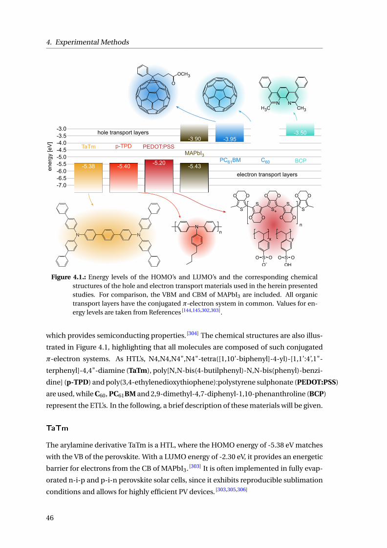
4. Experimental Methods
-3.0-3.5-4.0-4.5-5.0-5.5-6.0-6.5-7.0
ener
gy
[eV
]
-3.50
-4.10-3.95-3.90
-5.43-5.20
-5.40-5.38
TaTm p-TPD PEDOT:PSSMAPbI3
PC61BM C60 BCP
N N
Nn
n
S
O-OO
x
S
OH
OO
y
S
OO
S
OO
S
OO
S
OO
S+
OO
NNCH3H3C
OCH3
O
hole transport layers
electron transport layers
Figure 4.1.: Energy levels of the HOMO’s and LUMO’s and the corresponding chemicalstructures of the hole and electron transport materials used in the herein presentedstudies. For comparison, the VBM and CBM of MAPbI3 are included. All organictransport layers have the conjugated π-electron system in common. Values for en-ergy levels are taken from References [144,145,302,303].
which provides semiconducting properties. [304] The chemical structures are also illus-
trated in Figure 4.1, highlighting that all molecules are composed of such conjugated
π-electron systems. As HTL’s, N4,N4,N4",N4"-tetra([1,10’-biphenyl]-4-yl)-[1,1’:4’,1"-
terphenyl]-4,4"-diamine (TaTm), poly[N,N-bis(4-butilphenyl)-N,N-bis(phenyl)-benzi-
dine] (p-TPD) and poly(3,4-ethylenedioxythiophene):polystyrene sulphonate (PEDOT:PSS)
are used, while C60, PC61BM and 2,9-dimethyl-4,7-diphenyl-1,10-phenanthroline (BCP)
represent the ETL’s. In the following, a brief description of these materials will be given.
TaTm
The arylamine derivative TaTm is a HTL, where the HOMO energy of -5.38 eV matches
with the VB of the perovskite. With a LUMO energy of -2.30 eV, it provides an energetic
barrier for electrons from the CB of MAPbI3. [303] It is often implemented in fully evap-
orated n-i-p and p-i-n perovskite solar cells, since it exhibits reproducible sublimation
conditions and allows for highly efficient PV devices. [303,305,306]
46

4.1. Materials
p-TPD
Another wide band gap semiconducting arylamine, which is also serves as an HTL, is
p-TPD. It consists of a nitrogen atom with three aryl groups and belongs to the class of
polymers. With a HOMO level of -5.4 eV, it demonstrates good band alignment for the
injection of holes from the perovskite. Additionally, the LUMO energy of -2.4 eV en-
ables an efficient blocking of electrons. Its first implementation in perovskite PV was
reported in 2013 by Malinkiewicz et al. [302] It developed into a frequently used trans-
port material, not only in perovskite PV, [307,308] but also in the field of organic LEDs. [309]
After the preparation of thin p-TPD layers, the material displays hydrophobic character
due to the butylene group, which complicates the perovskite deposition on top, since
perovskites precursors are typically dissolved in hydrophilic solvents (see Section 4.2).
To overcome the wetting issue, several strategies [310,311] have been proposed, like the
additional deposition of an amphiphilic interfacial compatibilizer between p-TPD and
the perovskite. [308]
PEDOT:PSS
The last HTL is the water-based PEDOT:PSS, which is a mixture consisting of two com-
ponents. Figure 4.1 shows the chemical structure of the individual ingredients, with
the upper structure representing the PEDOT and the lower structure the PSS. The con-
jugated polymer PEDOT is consists of polythiophene and is mainly responsible for the
high electrical conductivity with values up to 4600 S/cm, [312] while the PSS counter-
part is based on polystyrene sulfonate. In thin films, both polymers are strongly inter-
linked, which results in a high transparency in the visible part of the electromagnetic
spectrum. Furthermore, by tuning the PEDOT:PSS ratio, the conductivity can be con-
trolled over several orders of magnitude. [313] In aqueous solution, PEDOT:PSS forms
micelles, with PSS forming the interface to H2O molecules while PEDOT is embedded
in the inner part of the aggregates, which leads to a high solubility and excludes toxic
solvents. [314] Over the past decades, these properties have contributed to the develop-
ment of PEDOT:PSS into a frequently encountered material in organic and perovskite
solar cells. [315,316]
C60
Nowadays, a large number of different fullerenes exists with the most popular being the
buckminsterfullerene C60. For its discovery in 1985, Kroto and coworkers were awarded
the Nobel Prize in chemistry in 1996. [317] Within a short period of time, considerable
improvements in synthesis have contributed to the fact that the material could be pro-
47

4. Experimental Methods
duced in larger quantities and thus also studied more easily. [318,319] It consists of 60
carbon atoms, which together form 12 pentagons and 20 hexagons arranged in an
spherical configuration, for which reason the molecule is often called buckyball. Due
to its high electron affinity, it is often employed as a electron transport layer in per-
ovskite solar cells. Electron mobilities in the range of 10−3 – 10−2 cm2/(Vs) are usually
reported [320,321] in combination with diffusion lengths of 400 nm allowing for sufficient
transport in PV devices. [322] Furthermore, the material features a LUMO energy match-
ing to the CB of the perovskite and has a band gap of about 1.9 eV. [323] Since it is not
soluble in organic solvents, it is usually deposited by thermal evaporation, as shown in
Section 4.2.
PC61BM
In order to make the C60 molecule solution processable, Hummelen et al. synthesized
PC61BM, which is functionalized with a phenyl and methyl butyrate side chain. [324]
This chain increases the solubility in organic polar solvents and leaves the optoelec-
tronic properties of pure C60 almost unaffected. Both, the energy levels and the elec-
tron mobilities are similar in both fullerene derivates. [302,321,325] The molecule has a
successful history in OPVs, as it has been applied as an electron acceptor for many
years until the efficiency was outnumbered by introducing fullerene-free acceptors. [14,15]
Together with the C60 and other fullerene derivates, it is one of the most commonly
used ETL’s in perovskite PV.
BCP
With a LUMO energy of -3.5 eV, BCP is not considered as a conventional transport layer,
but acts as a buffer layer between the fullerene and the metal electrode. It was of-
ten employed in OPVs to reduce recombination losses at the acceptor-electrode inter-
face [326] and therefore also adopted for perovskite solar cells. Even though its working
principle is not yet fully understood, recent studies suggest that thin BCP layers reduce
undesired charge accumulation in the ETL and replace the Schottky barrier with an
ohmic contact, which increases the PCE and improves device stability. [327,328]
4.2. Device Preparation
Intensive research over the past years has allowed the development of various methods
for the preparation of perovskite solar cells. All devices studied in this work were fab-
ricated in a planar device configuration as depicted in Figure 2.4b. For this approach,
48

4.2. Device Preparation
a glass substrate coated with ITO provides the basis (VisionTek Systems Ltd., United
Kingdom). With typical film thickness of only 100 – 200 nm, ITO exhibits a high average
transmission in the visible range of up to 92 % and a low specific electrical resistance
in the order of 10−4 Ωcm. [329] In order to define the active area precisely and prevent
short circuits when contacting the device, the substrate is patterned with a chemical
photolithography process. Afterwards, the substrate is prepared for further process-
ing by different cleaning steps. It is cleaned for 10 minutes each in water, acetone and
isopropanol before being treated for 30 seconds in an oxygen plasma to completely re-
move organic contamination.
Preparation of the HTL
An HTL is first deposited on the cleaned glass substrate. As already mentioned in the
previous section, this can be either TaTm, p-TPD or PEDOT:PSS. In case of TaTm (No-
valed, Germany), the substrate is transferred to a vacuum chamber integrated into a
nitrogen-filled glovebox and evacuated to a pressure of ≈ 10−6 mbar. The material are
then sublimed at temperatures around 250 °C to achieve a constant evaporation rate of
0.5 Å/s. The evaporation rate and thickness (10 – 50 nm) are controlled by quartz crys-
tal microbalance sensors. In contrast, p-TPD and PEDOT:PSS are processed from solu-
tion via spin coating. p-TPD (1-Material, Canada) is dissolved in 1,2-Dichlorbenzene
with a concentration of 7 mg/ml and spin cast in an inert nitrogen-filled glovebox re-
sulting in a layer thickness of 10 nm. Afterwards, the substrates is annealed at 110 °C to
remove residual solvent. Aqueous PEDOT:PSS solution (Clevios™ P VP AI 4083, Her-
aeus, Germany) is deposited (40 nm) under ambient conditions without any further
modification and annealed at 130 °C inside the glovebox.
Preparation of the Perovskite
The herein investigated perovskite layers are prepared by various methods, as schemat-
ically illustrated in Figure 4.2. Most methods involve the use of lead iodide (PbI2) and
methylammonium iodide (CH3NH3I or MAI) as reactants, whereby the formation of
the perovskite is described by the reaction equation
PbI2 +CH3NH3I −−→ CH3NH3PbI3. (4.1)
Similar to the HTL’s, perovskite films can be prepared either from solution or by ther-
mal evaporation in a inert nitrogen-filled glovebox. When processing from solution, a
distinction is made between the one-step and the two-step process. At the beginning
of the one-step process, often denoted as the mixed precursor approach, a PbI2 (Sigma-
49
4. Experimental Methods
Aldrich, Germany) stock solution is prepared by dissolving 1.5 mol in a 4:1 volume mix-
ture of N,N-Dimethylformamide (DMF) and Dymethylsulfoxide (DMSO) and stirred
over night on a hotplate adjusted to 25 °C. Afterwards, a small amount of MAI (Lumtec,
Taiwan) is added to a second vial. Shortly before use, the PbI2 solution is heated to
180 °C to ensure that the lead iodide is completely dissolved. After cooled down to
room temperature again, the PbI2 solution is added to the MAI vial such that the molar
ratio between PbI2 and MAI is 1:1 to obtain the required ratio from Equation 4.1. The
resulting PbI2/MAI solution is than stirred for at least 2 hours to ensure optimum in-
termixing and deposited by spin casting. During rotation of the spin coater, additional
(non-dissolving) solvent (usually Chlorbenzene) is dispensed on the sample to wash
out the solvents from the perovskite solution. Since the solvent is not dissolving the
perovskite, but helps to remove the other solvents, the procedure is often referred to as
anti-solvent washing. Introduced in 2014, it is considered as a major breakthrough in
the preparation of perovskite films as it improves the horizontal growth conditions and
reduces unwanted vertical elevations, resulting in much smoother and more homoge-
neous layers. [330–332] Further, it also increases the device reproducibility. The substrate
is then annealed at 100 °C for 15-30 minutes to remove residual solvents and allow for
full perovskite conversion. Further details on the application of the one-step approach
can be found in Reference [333].
In the two-step process, which has been established by Xiao et al. in 2014, two indi-
vidual solutions have to be prepared. [334] First, a 600 mg/ml solution of PbI2 in DMF is
prepared and stirred over night at 70 °C before use. The solution is then spin cast on
the substrate, followed by an annealing step of 15 minutes at 70 °C. After cooled down
to room temperature, a MAI solution (40 mg/ml in Isopropanol) is deposited by spin
coating. It is important to use an orthogonal solvent in this to prevent the dry PbI2
layer from being washed away. The substrate is then annealed at 100 °C for 1 hour to
start the interdiffusion process and allow for the chemical reaction between the two
layers. However, this approach often suffers from low PCE values and an insufficient
reproducibility due to unreacted PbI2 at the bottom of the substrate. To avoid this is-
sue, it was suggested to add a small amount of MAI already to the PbI2 solution. [335,336]
In this case, MAI is already present in the PbI2 layer leading to a larger disorder and
therefore an increased volume of the crystal. If the MAI solution is spin coated in the
next step, it is easier for the MAI to penetrate trough and react with the PbI2 leading
to an accelerated conversion and less unreacted salts afterwards. The best results are
usually obtained with a molar ratio of 0.2 with respect to PbI2. In addition, it has been
shown that it is beneficial to anneal perovskites in DMSO solvent vapor atmosphere in
order to increase the domain size of the polycrystalline layers and ensure a complete
50

4.2. Device Preparation
One-step deposition: mixed precursor
Two-step deposition: interdiffusion
Thermal evaporation:
100°CPbI2 MAI
+
PbI2
70°C
MAI
100°C
PbI2 MAI
Figure 4.2.: Overview of different fabrication methods for perovskite films. Perovskite lay-ers can be prepared either by dissolving both salts (PbI2 and MAI) and depositing thesolution via spin-coating or by applying thermal evaporation. Solution-based meth-ods are usually divided into one-step and two-step deposition. Further explanationsare provided in the main text.
reaction. [118] For this reason, the substrate is annealed at 100 °C in a closed metal box
with a few µl of DMSO after spin coating the MAI salt. Both modifications (adding a
small amount of MAI in the PbI2 solution and annealing in a solvent atmosphere) im-
prove the PCE and reproducibility of the solar cells noticeably and are applied to all
studied devices in this work, which were prepared by the two-step approach.
The third method for preparing thin perovskite layers is thermal evaporation. Two
crucibles, one filled with PbI2 (TCI Chemicals, Japan) and the other one filled with MAI
(Lumtec, Taiwan) are heated in an evacuated evaporation chamber under a pressure
of 10−6 mbar. To achieve evaporation rates of 0.5 Å/s for PbI2 and 1.0 Å/s for MAI, the
crucibles were heated to 250 °C and 70 °C, respectively. The co-deposition of both ma-
terials leads to perovskite films, where the thickness can easily be controlled via the de-
position time. To obtain homogenous substrate coverage, the substrate holder, which
51

4. Experimental Methods
is located above both crucibles, is rotating during evaporation. All fully evaporated
perovskite solar cells studied in this work are prepared by the group of Dr. Henk Bolink
from the University of Valencia (Spain). Further information on vapor-deposited per-
ovskites is provided in Reference [337].
Preparation of the ETL
After the preparation of the perovskite film, the electron transport layers are deposited.
If the perovskite absorber is prepared by spin coating, it is necessary to smooth the sur-
face with a 20 nm PC61BM (Solenne, Netherlands) layer. For this reason, a 20 mg/ml
solution from 1,2-Dichlorbenzene is spin cast on the perovskite, followed by anneal-
ing for 1 hour at 100 °C resulting in a film thickness of 10-20 nm. In the next step, the
substrate is transferred into an evaporation chamber, where 20 nm of C60 (Solenne,
Netherlands), 8 nm BCP (Sigma-Aldrich, Germany) and a 60 nm gold electrode are de-
posited via evaporation under a pressure of 10−6 mbar. The evaporation rate is kept
constant at ≤ 0.5 Å/s for C60 and BCP, but is higher for the gold (≥ 1.0 Å/s). In case of
fully evaporated solar cells, C60 (Sigma-Aldrich, Germany) is directly employed on top
of the perovskite layer with an evaporation rate of 0.5 Å/s until a thickness in the range
of 10 and 50 nm is reached.
4.3. Transient Electrical Techniques
The following section briefly introduces the transient electrical methods which are ap-
plied in this thesis to study charge carrier recombination processes in perovskite solar
cells. In complete devices, charge carrier recombination parameters, like the charge
carrier lifetime or the density are not directly accessible. For this reason, steady-state
and transient behavior of Voc is often studied, since charge carrier generation equals
recombination under open-circuit. As discussed in Chapter 3, first insights on re-
combination can be already obtained by determining the diode ideality factor. To
gain further information, both charge carrier lifetime and the corresponding density
are herein measured with optoelectrical methods. All time-resolved measurements
are performed in a closed-cycle helium cryostat to avoid water-induced degradation
processes within the solar cells and precisely control the device temperature (by a
Lakeshore 332 cryogenic temperature controller). In order to obtain recombination
parameters for different open-circuit voltages, the illumination intensity is varied over
several orders of magnitude. For all measurements, a high power LED array, which
is driven by a Keithley 2602 Source Meter, is employed to generate steady-state illu-
mination conditions. To calibrate the LED current, jsc of every device is first mea-
52

4.3. Transient Electrical Techniques
sured in an inert glovebox under a simulated AM1.5 G spectrum with an irradiance of
100 mW/cm². Then, the device is transferred into the cryostat and the LED current is
adjusted such that the device generates the same jsc as previously determined in the
glovebox. This intensity is defined as 1 sun illumination. The intensity can be changed
by varying the LED current and using neutral density filters.
4.3.1. Open-Circuit Voltage Decay
Open-Circuit Voltage Decay (OCVD) experiments are a simple tool to study internal
recombination losses in solar cells. First recombination studies by employing voltage
decay measurements on germanium were conducted already in 1955 by Lederhandler
and Giacoletto. [338] After broad application in classical pn-junctions, OCVD was also
adopted to study charge carrier dynamics in DSSCs, [339,340] OPVs [341] and very recently
in perovskite solar cells. [342]
A schematic presentation of the measurement procedure is shown in Figure 4.3. Dur-
ing the whole experiment, the device is kept under open-circuit conditions via a 1 TΩ
high-impedance voltage amplifier (Femto Messtechnik GmbH). The solar cell is then
illuminated with a LED to generate an excited carrier population which leads to an
open-circuit voltage. It is important to illuminate for a sufficiently long time (usually
in the order ms to s) to ensure that steady-state conditions are reached in the device.
At time t0, the illumination source is turned off and the voltage decay is monitored as
illum
inat
ion
time
open
-circ
uit v
olta
ge
timet0
0
0
Figure 4.3.: Working principle of OCVD measurements. A solar cell is kept under open-circuit and illuminated with a constant light source. After reaching steady-state con-ditions, the light is switched off and the voltage decay is recorded as a function oftime. The resulting decay curve can be analyzed by using Equation 4.3 to obtain thecarrier lifetime τOCV D .
53

4. Experimental Methods
a function of time using an Agilent Infinium 90254A digital storage oscilloscope. Since
electrical current is impeded all the time, the only way for charge carriers to relax back
to their equilibrium states is via recombination processes inside the device. Voc is then
affected by the decreasing carrier density since it follows the relationship
Voc = kB T
q· ln
(np
n2i
). (4.2)
This expression can be directly obtained, if Equations 3.14 and 3.15 are multiplied with
each other and NC NV ·exp(− Eg
kB T
)is replaced by n2
i . Since recombination processes are
not instantaneous, the time evolution of the open-circuit voltage allows conclusions to
be drawn regarding the charge carrier lifetime. As previously demonstrated in a various
publications, [340,343,344] the charge carrier lifetime τOCV D can be determined from the
slope of the voltage decay according to
τOCV D =−ni d kB T
q
(dVoc (t )
dt
)−1
. (4.3)
The main benefit of employing lifetime determination from OCVD signals arises from
the fact that it is a continuous measurement providing high resolution in voltage and is
collected in short time. All OCVD results shown in this work were usually averaged over
4 – 8 individual measurements to increase the signal-to-noise ratio, which is important
for the analysis of the data. To increase the signal quality even further, additional math-
ematical smoothing is employed prior to taking the derivative.
4.3.2. Transient Photovoltage
Another possibility to determine the charge carrier lifetime in solar cells is the small-
signal method Transient Photovoltage (TPV). The basic idea of the method can be
dated back to 1955, where it was developed to study germanium and silicon. [345] The
method experienced great attention during the last decade in the investigation of novel
thin-film solar cells such as OPVs [346,347] and perovskites. [348,349]
A simplified overview on the working principle is provided in Figure 4.4. A solar cell
is first illuminated with constant bias light and kept under open-circuit conditions dur-
ing the whole measurement by using the same experimental setup as for OCVD mea-
surements. The steady-state Voc is then perturbated by a small optical pulse gener-
ated by a Nd:YAG (neodymium-doped yttrium aluminium garnet) laser (λ = 532 nm,
EKSPLA PL-2210) with a pulse duration of 80 ps. Upon laser excitation, the addition-
ally created charge carriers lead to an increase in voltage ∆Voc . In order to maintain
54

4.3. Transient Electrical Techniques
quasi-equilibrium conditions, the laser intensity is attenuated with neutral density fil-
ters such that the relation ∆Voc ¿ Voc holds, which is relevant for further evaluation
of the voltage transient as will be explained in the next paragraph. Since the device is
kept under open-circuit conditions the whole time, the additionally generated charge
carriers ∆n have to recombine until the steady-state carrier concentration originating
from the bias LED light is reached again.
The small optical perturbation leads to an increased total charge carrier density,
which can be expressed as n +∆n. With insertion into Equation 3.1 it follows
d(n +∆n)
dt=−(
k1(n +∆n)+k2(n +∆n)2 +k3(n +∆n)3)=−
[k1n
(1+ ∆n
n
)+k2n2
(1+ ∆n
n
)2
︸ ︷︷ ︸1+2
(∆nn
)+(∆nn
)2
+k3n3(1+ ∆n
n
)3
︸ ︷︷ ︸1+3
(∆nn
)+3(∆nn
)2+(∆nn
)3
]. (4.4)
Considering the small-perturbation approximation ∆Voc ¿ Voc such that ∆n ¿ n, all
terms (∆nn )x with x being larger than 1 are neglected and the expression can be rear-
ranged
d(n +∆n)
dt≈−
[k1n
(1+ ∆n
n
)+k2n2
(1+2
∆n
n
)+k3n3
(1+3
∆n
n
)]=−[
k1n +k2n2 +k3n3]︸ ︷︷ ︸dndt
−∆n[k1 +2k2n +3k3n2]︸ ︷︷ ︸
ke f f
.(4.5)
The first bracket can be identified as the rate equation without the small perturba-
tion, while the second bracket is independent of ∆n and can be treated as an effective
recombination coefficient ke f f . Thus, the recombination rate for the additionally gen-
erated charge carriers (being proportional to ∆Voc can be written as
d∆Voc
dt∝ d∆n
dt≈−ke f f ∆n = ∆n
τ∆n. (4.6)
Here, ke f f is expressed by the small-perturbation lifetime τ∆n . Solving the differential
equation yields an exponential relationship between ∆n and τ∆n according to
∆n =∆n0 exp
(− t
τ∆n
)(4.7)
and the measurable voltage decay back to the steady-state Voc via
Voc (t ) =Voc +∆Voc exp
(− t
τ∆n
). (4.8)
55

4. Experimental Methods
illum
inat
ion
time
open
-circ
uit v
olta
ge
timet0
0
0
laser
Voc
Voc
VocVoc
Figure 4.4.: Schematic illustration of an TPV experiment. The solar cell is kept under open-circuit conditions and illuminated with constant background illumination. At t = t0,a short laser pulse generates additional charge carriers in the device such that thevoltage rises by ∆Voc . If the small perturbation meets the requirement ∆Voc ¿ Voc ,the resulting voltage transient can be used to determine the charge carrier lifetimeat the particular background illumination/open-circuit voltage.
By fitting the measured voltage transient with an exponential decay, the charge carrier
lifetime can be determined as a function of illumination/open-circuit voltage. Usually
TPV experiments are conducted at a multitude of different background illumination in-
tensities, where ∆Voc ≈ 5 – 15 mV to meet the requirement ∆Voc ¿Voc . The advantage
of TPV consists in the simpler evaluation with an exponential fit function compared to
OCVD, where the derivative of an large and equally noisy transient signal needs to be
calculated. In order to increase the signal quality also for TPV, a transient is recorded
100 times and then averaged. Since the measured lifetimes are a function of Voc and
therefore n, the equally important parameter of carrier density needs also to be deter-
mined to correctly understand recombination dynamics under operating conditions.
4.3.3. Charge Extraction
Charge Extraction (CE) is often selected to determine the charge carrier density in a
solar cell under a specific illumination intensity. [249,350–352] A CE experiment is con-
ducted directly after TPV at the same illumination intensity to correlate the obtained
values with each other. Prior to each measurement, an j -V measurement under il-
lumination is performed (Keithley 2602 Source Meter) to identify Voc . The CE proce-
dure itself is divided into two different steps, as illustrated in Figure 4.5: first, the so-
lar cell is illuminated with constant light and the previously measured Voc is applied,
56

4.3. Transient Electrical Techniques
-
+
perovskite
perovskite HTL
EFn
EFp
ETL
+ + + + + +
- - - - - -
illum
inat
ion
time
volta
ge
time
- - -
+ + +band
str
uctu
recu
rre
nt
timet0
0
0
0
Voc
open-circuit short-circuit
extracted charge Qext
EFn
EFp
EF
-
++
--
+
perovskiteETL
perovskite HTL
-
+
+
-
Figure 4.5.: Simplified scheme of a CE experiment. In the first step, the solar cell is illumi-nated with a constant illumination source and the measured Voc is applied. Underthese conditions, no current is flowing and the device is under open-circuit. In thesecond step, the illumination source is turned off and the solar cell is simultane-ously switched from open-circuit to short-circuit conditions. The resulting currenttransient is then recorded, integrated and normalized to the volume of the activearea to calculate the charge carrier density, which was stored in the device under theparticular illumination intensity.
such that the device is kept under open-circuit and a steady-state carrier population is
generated. At t = t0, the illumination source is turned off and the device is simultane-
ously switched to short-circuit conditions. This is realized by a fast Texas Instruments
SN74LVC1G3157 analog switch (with response time of 3 ns), which is triggered by an
Agilent 81150A pulse generator. The resulting current transient is amplified by a Femto
DHPCA-100 current-voltage amplifier and recorded by the same digital storage oscillo-
scope as used for OCVD and TPV. The current transient is then averaged 15 times to im-
57

4. Experimental Methods
prove the signal-to-noise ratio. By integrating the obtained current to get the extracted
charge Qext , the charge carrier density stored inside the device under the particular
illumination intensity can be calculated via
n = Qext
Ad q= 1
Ad q
∫ tstop
t0
I (t ) dt , (4.9)
where A is the active area of the device, which is defined by the overlap of ITO and
the metal electrode (see Section 4.2). The thickness d of the active layer is individ-
ually measured for every solar cell with a Veeco Dektak 150 profilometer. The time
tstop is defined by the moment, where I (tstop ) ≈ 0, which is typically reached on the µs
timescale for perovskite solar cells. The combination of both TPV and CE measured at
the same illumination conditions allows for a detailed analysis of recombination losses
in fully working devices under operating conditions and provides a powerful toolbox to
determine the rates and orders of recombination processes.
However, the recorded current transients do not necessarily have to originate from
charge carriers inside the active layer, but also can be affected by charges stored in the
transport layers or at the electrodes. For this reason, additional measurements are per-
formed in the dark to account and correct for these capacitive charge carriers. The ex-
act procedure and discussion will be provided in Section 5.6 and the general influence
of capacitive effects on the introduced transient electrical techniques will be studied in
Chapter 5.
58

5. Capacitive Eects in Transient
Electrical Measurements
P3HT:PCBM PCDTBT:PCBM MAPbI3
-+
+
- - - -
+ + +anode
cathode
capRseries
Rshunt
C-
+
Abstract. Lifetime evaluation of so-
lar cells is frequently conducted via
both optical and electrical means
with the purpose of obtaining a
deeper understanding of the dom-
inant performance limiting recom-
bination mechanisms. Here, these
previously assigned lifetimes are re-
evaluated as often being severely in-
fluenced by capacitive decay rates of spatially separated charge carriers. This
misconception hence explains the sometimes observed irregularities between
optically and electrically determined lifetimes. In addition, it is revealed that
not only the lifetimes determined by OCVD and TPV, but also charge carrier
densities derived from CE measurements can be affected by capacitive charge
carriers. It is shown that capacitive effects are very often ruling these mea-
surements and therefore interfere with the assignment of important recom-
bination parameters. To explore this limitations in more detail, an analytical
expression outlining under which conditions relevant bulk recombination pa-
rameters are electrically accessible in thin-film solar cells is provided. In order
to make general statements regarding different PV devices, the study includes
not only perovskite solar cells, but comprises also other technologies such as
OPVs and Si solar cells.
This chapter is partially based on
D. Kiermasch, A. Baumann, M. Fischer, V. Dyakonov and K. Tvingstedt. Revisiting lifetimes from tran-
sient electrical characterization of thin film solar cells; a capacitive concern evaluated for silicon, organic
and perovskite devices. Energy & Environmental Science, 11, 629-640 (2018). DOI: 10.1039/C7EE03155F
59

5. Capacitive Effects in Transient Electrical Measurements
5.1. Introduction
Thin film solar cells made from novel materials with high absorption coefficients are
generally much cheaper to produce than their thicker counterparts and therefore rep-
resent a promising alternative to low-cost large-scale electricity production. However,
thin solar cells made from innovative materials such as organics or metal halide per-
ovskites need to have high PCE’s to be able to compete with the already commer-
cially established technologies. To grasp what limits the voltage produced by solar cells
under illumination, it is necessary to understand the mechanisms behind the disap-
pearance rate of the photogenerated electrons and holes in the device. The build-up
and disappearance of charge carrier densities in solar cells involve a variety of pro-
cesses including absorption and charge carrier generation, separation, transport via
drift and diffusion, recombination in the bulk, via traps, at the surfaces or from the
electrodes themselves. All these processes occur on a time scale ranging from sub-
picoseconds [353,354] to in some cases several seconds or even hours. [355] Effectively
designing PV components for optimized PCE always relies on maximizing the carrier
generation and transport processes and simultaneously minimizing the recombina-
tion processes towards the radiative limit of the corresponding material. [354]
The lifetime of photogenerated charge carriers is one of the most important param-
eters in solar cells, as it rules the recombination rate that defines the open-circuit volt-
age (see Chapter 3) and the required minimum extraction time. Identifying the dom-
inant recombination mechanism and the corresponding rate (lifetime) is accordingly
an important subject of any PV researcher, independent of material and technology.
Both optical and electrical transient measurements are therefore frequently employed
with the purpose to approach this. Contactless optical methods such as terahertz spec-
troscopy, [356] transient absorption, [357] transient photoluminescence, [91,358–361] and tran-
sient microwave photoconductivity [92,362] all provide information related to the overall
disappearance rate of excited states or charge carriers in the active material. These
methods are widely performed on pure absorber materials without transport layers
and at excitation intensities that differ from operating conditions. Direct electrical
measurements on PV materials embedded in a device configuration probe instead the
disappearance rate of excess carrier densities and the corresponding quasi Fermi level
splitting as introduced in Section 4.3. Monitoring the rate at which this property decays
provides accordingly the sought-after information of how the associated excess charge
carriers disappear in a solar cell. In the time-domain, the most common methods em-
ployed are based on measuring the decay of Voc , either by the full signal OCVD method
or by the small-perturbation technique of TPV. In the corresponding frequency-domain,
60
5.1. Introduction
the rates are monitored by impedance spectroscopy [363–366] or intensity modulated
voltage or current spectroscopy. [237] All rate determination methods need a comple-
mentary technique to identify the relationship between carrier density and voltage. In
case of the time-domain methods, this is provided by either combining Transient Pho-
tocurrent (TPC) with TPV (usually referred to as Differential Charging) or alternatively
by the CE method. The frequency-domain-methods rely instead on the integral of var-
ious forms of differential capacitance–voltage measurements. [364,367] Both the time-
domain and frequency-domain methods are therefore in principle able to determine
the charge carrier lifetime as a function of carrier density.
However, there is caveat with these methods originating from that they were initially
developed for thicker indirect band gap germanium or silicon solar cells. [338] Devices
comprising these inorganic crystalline materials are very different compared to many
novel thin-film solar cells mostly in terms of their carrier lifetimes, but also in their
band gaps, thicknesses, capacitances and layouts. Thin-film solar cells are necessar-
ily relying on materials with higher absorption coefficients leading to active layer film
thickness in the range of 20 – 500 nm. The high absorption coefficient allows a smaller
thickness that however leads to devices with larger (geometric) capacitance values.
Electrical characterization methods employed to determine recombination dynamics
under operating conditions are therefore not always easily transferable to new genera-
tion thin-film PV devices.
Charge carrier lifetimes determined from the analysis of electrical transients are for
most of the mentioned PV technologies ranging typically from 1 microsecond at sun
intensities up to several milliseconds or even seconds at reduced intensities. These
long lifetimes of excess charge carriers are quite peculiar, as they are several decades
longer than those determined via complementary optical measurements such as tran-
sient photoluminescence. This discrepancy in lifetimes has not only been frequently
observed in OPVs, [368,369] but also in perovskite solar cells during the last years. [370,371]
Both optical and electrical methods are claiming to probe charge carrier lifetimes rel-
evant for steady-state conditions, but obviously cannot both be correct if determined
at equal carrier densities. In addition, a strong non-linear dependence of charge car-
rier lifetimes on voltage is observed, when transient electrical methods are employed
to study recombination losses. The observed strong dependence on illumination in-
tensities has been interpreted as that the dynamics cannot be described by first-order
recombination processes, where the lifetime should be constant over at least a small
range of excess carrier densities (and consequently Voc ’s). In case of DSSCs, the very
long lifetimes up to several seconds [340] are generally attributed to a slow second-order
chemical reaction rate between electrons and ions present in the electrolyte. However,
61

5. Capacitive Effects in Transient Electrical Measurements
CBM
VBM
-
+
-
+
photon
-
shallow traps
(i) (ii) (iii)- -
(iv)
deep trap
Figure 5.1.: Principle of increased carrier lifetimes by carrier trapping and detrapping pro-cesses. An electron is trapped and released at shallow traps, which do not act as SRHrecombination centers until it finally recombines radiatively or non-radiatively via adeep trap. This procedure can prolong the effective carrier lifetime.
a quite identical dependence is also observed in most organic and perovskite based
solar cells studied so far. In these solid-state components, slow chemical reactions are
not suitable to generally explain the charge carrier kinetics. A power law dependence
of recombination rates with second- or higher-order recombination kinetics in combi-
nation with assumptions of trapped charges in a broad DOS has often been ascribed to
account for both the strong dependency of voltage and the very long lifetimes. In this
common picture, the long lifetimes originate from a non-linear relationship between
trapped and free charges, where shallow traps slow down the overall recombination
rate and not speed up recombination as it is generally the case for deep mid gap trap
states. [370] This trapping-detrapping procedure is illustrated in Figure 5.1, where an
electron gets trapped and detrapped until it recombines radiatively with a hole or non-
radiatively via a deep trap. However, it is unclear why the long lifetimes often occur
exclusively in electrical measurements on devices while optical methods are not af-
fected. Obviously, the presence of transport layers and electrodes influences the mea-
sured lifetimes.
In this chapter, both theoretical and experimental evidence is provided for that car-
rier trapping is not responsible for the slow recombination rates often encountered
in thin-film solar cells. Charge carrier lifetimes are determined via both OCVD and
TPV methods on a multitude of different PV technologies indicating that some of the
obtained lifetimes are very often associated with a capacitive discharging rate instead
of bulk recombination in the active layer. In addition, it is revealed that the same ef-
fects also influence CE experiments, which also complicates the determination of the
corresponding charge carrier densities. The objective of this study is therefore to ex-
perimentally clarify the general influence of quasi-static capacitive effects on charge
carrier lifetime and density determination by electrical time-domain approaches.
62
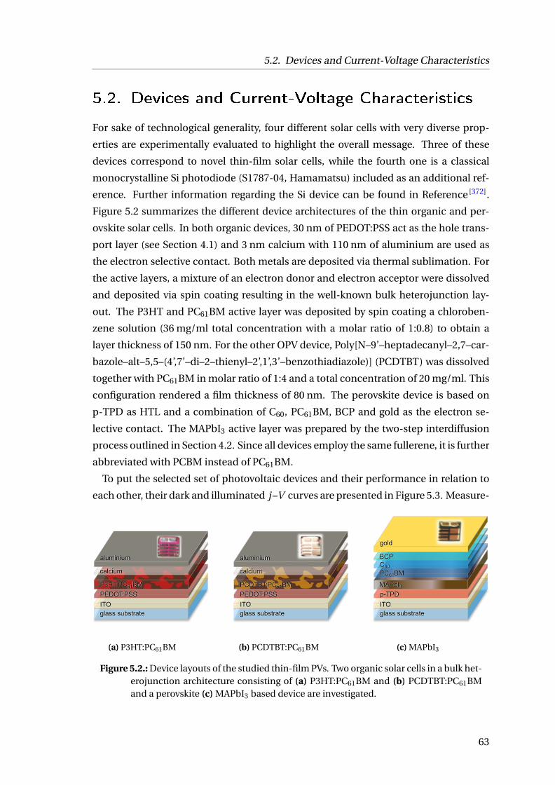
5.2. Devices and Current-Voltage Characteristics
5.2. Devices and Current-Voltage Characteristics
For sake of technological generality, four different solar cells with very diverse prop-
erties are experimentally evaluated to highlight the overall message. Three of these
devices correspond to novel thin-film solar cells, while the fourth one is a classical
monocrystalline Si photodiode (S1787-04, Hamamatsu) included as an additional ref-
erence. Further information regarding the Si device can be found in Reference [372].
Figure 5.2 summarizes the different device architectures of the thin organic and per-
ovskite solar cells. In both organic devices, 30 nm of PEDOT:PSS act as the hole trans-
port layer (see Section 4.1) and 3 nm calcium with 110 nm of aluminium are used as
the electron selective contact. Both metals are deposited via thermal sublimation. For
the active layers, a mixture of an electron donor and electron acceptor were dissolved
and deposited via spin coating resulting in the well-known bulk heterojunction lay-
out. The P3HT and PC61BM active layer was deposited by spin coating a chloroben-
zene solution (36 mg/ml total concentration with a molar ratio of 1:0.8) to obtain a
layer thickness of 150 nm. For the other OPV device, Poly[N–9’–heptadecanyl–2,7–car-
bazole–alt–5,5–(4’,7’–di–2–thienyl–2’,1’,3’–benzothiadiazole)] (PCDTBT) was dissolved
together with PC61BM in molar ratio of 1:4 and a total concentration of 20 mg/ml. This
configuration rendered a film thickness of 80 nm. The perovskite device is based on
p-TPD as HTL and a combination of C60, PC61BM, BCP and gold as the electron se-
lective contact. The MAPbI3 active layer was prepared by the two-step interdiffusion
process outlined in Section 4.2. Since all devices employ the same fullerene, it is further
abbreviated with PCBM instead of PC61BM.
To put the selected set of photovoltaic devices and their performance in relation to
each other, their dark and illuminated j –V curves are presented in Figure 5.3. Measure-
PEDOT:PSS
ITOglass substrate
P3HT:PC61BM
calcium
aluminium
PEDOT:PSS
ITOglass substrate
PCDTBT:PC61BM
calcium
aluminium
PC61BMC60
BCP
gold
p-TPD
MAPbI3
ITOglass substrate
(a) P3HT:PC61BM (b) PCDTBT:PC61BM (c) MAPbI3
Figure 5.2.: Device layouts of the studied thin-film PVs. Two organic solar cells in a bulk het-erojunction architecture consisting of (a) P3HT:PC61BM and (b) PCDTBT:PC61BMand a perovskite (c) MAPbI3 based device are investigated.
63

5. Capacitive Effects in Transient Electrical Measurements
ments in the dark are presented on a logarithmic scale, while the illuminated curves are
depicted on a linear scale. In order to determine ni d and j0, the exponential term of the
Shockley Equation 2.8 is used as a fit function and the obtained values are summarized
in Table 5.1. The extracted ni d ’s vary from exactly one for the Si photodiode to exactly
two for the perovskite cell, with both OPV devices ranging in between. A closer look at
the illuminated j -V characteristics reveals that the PCDTBT:PCBM solar cell shows the
lowest PCE of 2.8 %. Both, the Si and the P3HT:PCBM devices have a PCE of 3.9 %, while
the perovskite solar cell is the most efficient device with a PCE of 12.2 %. In case of the
perovskite device, both the forward and backward measurements are shown, proving
that only minor hysteresis behavior can be observed.
10-7
10-6
10-5
10-4
10-3
10-2
10-1
100
101
102
curr
ent d
ensi
ty [A
/m²]
1.41.21.00.80.60.40.20.0
voltage [V]
Si P3HT:PCBM PCDTBT:PCBM MAPbI3 exp. fits
dark
-250
-200
-150
-100
-50
0cu
rren
t den
sity
[A/m
²]
1.41.21.00.80.60.40.20.0
voltage [V]
Si P3HT:PCBM PCDTBT:PCBM MAPbI3
1 sun
(a) (b)
Figure 5.3.: j -V characteristics for all four studied PV devices (a) in the dark and (b) un-der illumination. The grey dashed lines correspond to exponential fits accordingto Equation 2.8 in order to determine j0 and ni d . For the MAPbI3 solar cell, boththe forward and backwards scans are shown to illustrate only minor current-voltagehysteresis. All extracted PV parameters are summarized in Table 5.1
device ni d j0 [Am−2] jsc [Am−2] Voc [V] FF [%] PCE [%]Si photodiode 1.0 5.2 · 10−8 101 0.56 69 3.9P3HT:PCBM 1.3 4.6 · 10−7 99 0.63 62 3.9
PCDTBT:PCBM 1.7 1.7 · 10−8 58 0.90 52 2.8MAPbI3 2.0 4.2 · 10−8 198 1.10 56 12.2
Table 5.1.: Extracted PV parameters from Figure 5.3 for all studied devices from j -V charac-teristics in the dark and under 1 sun illumination.
64

5.3. Determination of Charge Carrier Lifetimes
5.3. Determination of Charge Carrier Lifetimes
In this section, charge carrier lifetimes are determined using transient electrical meth-
ods and different recombination regimes are identified. These techniques have ad-
vantages in comparison to optical measurements, as they are able to determine re-
combination dynamics on a wide range of timescales in fully working devices. Figure
5.4a shows normalized TPV transients in a semi-logarithmic plot for the set of stud-
ied devices. The background illumination intensity was adjusted to be 1 sun. The
decays of all thin-film devices are well-described by a single-exponential fit accord-
ing to Equation 4.8, revealing the shortest lifetime for the perovskite (τ = 0.39 µs) and
the longest transient for the P3HT:PCBM device (τ = 2.87 µs). The decays for the Si de-
vice are summarized in the inset, where the illumination intensity corresponds to 1 sun
and 0.001 suns. In case of the lower intensity, the data is fitted by a single exponential
function leading to τ = 142.7 µs, whereas at 1 sun illumination, a double exponential
nature is detected with time constant of τ1 = 2.53 µs and τ2 = 48.1 µs. OCVD transients
for the same devices are presented in Figure 5.4b. Prior to the decay, every device was
illuminated with 1 sun intensity. Quite different decay dynamics can be observed be-
tween the studied devices: for example, the P3HT:PCBM solar cell displays the shortest
0.01
2
4
6
80.1
2
4
6
81
∆Voc
[a.u
.]
2520151050
time [µs]
0.01
0.1
1
∆Voc
[a.u
.]
5004003002001000time [µs]
0.001 suns: 142.7 µs
48.1 µs
2.53 µs
Si P3HT:PCBM PCDTBT:PCBM MAPbI31 sun
2.87 µs 1.97 µs
0.39 µs1.2
1.0
0.8
0.6
0.4
0.2
0.0
open
-circ
uit v
olta
ge [V
]
10-6 10
-4 10-2 10
0 102
time [s]
Si P3HT:PCBM PCDTBT:PCBM MAPbI3
1 sun
(a) (b)
Figure 5.4.: (a) TPV decays for the studied thin-film PVs at an illumination intensity of 1 sun.The data is fitted with an exp. decay according to Equation 4.8 in order to extract theTPV lifetime τ. The logarithmic representation clearly shows that all decays are welldescribed by a single-exponential decay. This is contrary to the Si device, which isshown in the inset. Here, at low light intensities (0.001 suns), a single exponentialdecay is observed while at higher intensities (1 sun) a double-exponential decay ismeasured and hence two lifetimes can be extracted. (b) OCVDs for all devices, wherethe solar cells were illuminated with 1 sun prior to the decay.
65

5. Capacitive Effects in Transient Electrical Measurements
time to reach 0 V among the thin-film PVs even though its TPV lifetime is the longest
one. The perovskite and the Si device demonstrate the longest OCVD decays with up
to 115 s for the silicon device. Furthermore, all devices have different slopes strongly
depending on the time after the light was switched off which indicates differences in
the responsible recombination mechanisms during each decay.
To examine how the obtained TPV lifetimes scale with open-circuit voltage, mea-
surements are performed for a plethora of different logarithmically spaced steady-state
light intensities ranging from a minimum of 10−6 suns up to a maximum of 3 suns. It
is noted that for this range of intensities the requirement ∆Voc ¿ Voc is ensured for
every measurement (see Section 4.3.2). The determined lifetimes are plotted as a func-
tion of Voc in Figure 5.5a. In addition, OCVD lifetimes (solid lines) determined from
Figure 5.4b by applying Equation 4.3 are included. The obtained lifetimes vary from
a few hundred nanoseconds to even seconds for the range of measured open-circuit
voltages. It can be confirmed that the measured lifetimes and their relation to Voc in-
deed are identical within very respectable accuracy for all materials such that τT PV ≈τOCV D . TPV additionally provides two clearly identifiable lifetimes in the high-voltage
regime of the Si device, whereas the OCVD only succeeds in identifying the longer
lifetime. That the inverse derivative of the large signal OCVD generally equals small-
perturbation lifetimes from TPV or Intensity-Modulated Photovoltage Spectroscopy
(IMVS) was also observed for DSSC [340,344] and recently for perovskites. [373] After hav-
ing confirmed the overall identity between OCVD and TPV lifetimes in all four devices,
the general behavior of how the determined lifetimes relate to internal voltage is evalu-
ated. For the Si photodiode, two quite constant charge carrier lifetimes are found for all
voltages above 0.4 V. These lifetimes are individually associated with the thin back p-
layer and the front thicker n-layer. Accordingly, the recombination is truly of first-order
type with constant lifetimes in this regime as expected for heavily doped semiconduc-
tors. At lower voltages (< 0.4 V), only one value can however be recognized, where the
determined lifetime is rapidly increasing with decreasing voltage. The large set of TPV
illumination intensities as well as the OCVD measurements easily allow to identify that
in this region the logarithm of the lifetime scales linear with voltage. As it is impossi-
ble that the dominant recombination dynamics should make a transition from a first-
order process at high carrier densities to a higher-order process at low carrier densi-
ties, this cannot be the origin of the voltage-dependent lifetimes below 0.4 V. These
voltage-dependent lifetimes are also observed for the other PV devices. While the per-
ovskite solar cell shows an almost constant slope over the whole intensity range, both
organic devices exhibit regions of different slopes. In case of the PCDTBT:PCBM device,
a transition occurs from a nearly constant lifetime at voltages below 0.5 V to a steeper
66

5.4. Effect of External Conditions on Voltage Decay
10-7
10-5
10
-3
10-1
10
1
103
m
easu
red
lifet
ime
[s]
1.00.80.60.40.2
open-circuit voltage [V]
TPV OCVD / Si / P3HT:PCBM / PCDTBT:PCBM / MAPbI3
lifet
ime
[s]
open-circuit voltage [V]
S
i P
3HT
:PC
BM
PC
DT
BT
:PC
BM
MA
PbI
3
S
i (
P3H
T:P
CB
M)
P3H
T:P
CB
MP
CD
TB
T:P
CB
M
data
(i)(ii)(iii)
(a) (b)
Figure 5.5.: (a) Charge carrier lifetimes determined via TPV and OCVD for the four solarcells. Slope alterations lead to the presence of different regimes, where the lifetimescan be constant (at high or low voltages) or voltage-dependent (for intermediatevoltages). For a better overview, a simplified scheme of these different regimes isprovided in (b), where the solar cells are categorized according to the presence ofdifferent slope alterations.
slope for higher Voc ’s. A similar transition is visible for P3HT:PCBM at around 0.2 V
with the addition of another slope alteration being evident at roughly 0.5 V. A simpli-
fied scheme of the observed lifetime transitions is illustrated in Figure 5.5b. All devices
have the highest slope at intermediate voltages in common. However, both organic
cells demonstrate a transition to a more constant lifetime at low voltages, whereas the
Si and to a minor extend also the P3HT:PCBM solar cell exhibit another transition to
a constant lifetime at higher Voc ’s. To explain these different lifetime regimes, a com-
plete picture of the underlying recombination mechanisms will be developed in the
following based on experimental and theoretical results.
5.4. Eect of External Conditions on Voltage
Decay
To understand the electronic behavior of PV devices, research is very often based on
equivalent circuit modeling. This allows for a detailed description of all currents and
voltages present in a solar cell, which opens up the possibility to study the different
electrical components a solar cell consists of. In this section, the impact of these com-
ponents will be investigated in more detail to obtain a better understanding of how
they affect lifetime determination by transient electrical methods.
67

5. Capacitive Effects in Transient Electrical Measurements
Rseries
Rshunt
C
photogenerated
current
D
Figure 5.6.: Equivalent circuit of a solar cell. Photocurrent source, shunt resistance anda capacitor are connected in parallel to a diode. In addition, a series resistance isincluded. In order to describe real solar cells correctly, all these components need tobe considered.
Figure 5.6 displays a widely used equivalent circuit model for solar cells. In the ideal
case, a PV device can be described only by a photocurrent source, which generates the
current and a diode being connected in parallel. [374,375] Sometimes, additional diodes
are included to account for different recombination mechanisms. [170,376] In reality, such
ideal devices do not exist, since resistive losses are always present and have to be ac-
counted for by implementation of additional components in the equivalent circuit.
The influence of resistive losses is well-recognized in literature and often included in
the evaluation of j -V characteristics and other experimental observations. [355,374,377]
Since the transient electrical methods employed in this work are conducted under
open-circuit conditions, Rser i es does not affect these measurements and accordingly
can be ignored in further analysis. On the contrary, the capacitor connected in parallel
is only poorly considered in literature. Thin-film PVs consist of active layers with thick-
nesses of several hundred nanometers, which are embedded between two electrodes
leading to capacitances that are often not negligible. For this reason, the influence of
the capacitor on transient electrical methods is studied in this section. In addition, the
impact of Rshunt and the illumination intensity will be evaluated in order to obtain a
complete picture of all parameters and determine the conditions under which relevant
recombination parameters can be obtained.
Eect of Illumination Intensity
By first changing the starting steady-state voltage by employing different light intensi-
ties covering several decades, the influence of light intensity on OCVD can be exam-
ined. Figure 5.7 summarizes the decays for starting light intensities ranging between
10−6 and 2.7 suns. For the Si device, the curves can be separated into a fast recombina-
tion regime at early timescales (< 10−3 s) and a slower recombination regime, where all
measurements converge into the same decay at longer time scales. Although the start-
68

5.4. Effect of External Conditions on Voltage Decay
0.7
0.6
0.5
0.4
0.3
0.2
0.1
0.0
open
-circ
uit v
olta
ge [V
]
10-6 10
-4 10-2 10
0 102
time [s]
1 sun
10-1
suns
10-2
suns
10-3
suns
10-4
suns
10-5
suns
10-6
suns
intensity
Si
0.6
0.5
0.4
0.3
0.2
0.1
0.0
open
-circ
uit v
olta
ge [V
]
10-6 10
-4 10-2 10
0 102
time [s]
1 sun
10-1
suns
10-2
suns
10-3
suns
10-4
suns
intensity
P3HT:PCBM
(a) (b)
0.8
0.6
0.4
0.2
0.0
open
-circ
uit v
olta
ge [V
]
10-6 10
-4 10-2 10
0 102
time [s]
1 sun
10-1
suns
10-2
suns
10-3
suns
intensity
PCDTBT:PCBM
1.2
1.0
0.8
0.6
0.4
0.2
0.0
open
-circ
uit v
olta
ge [V
]
10-6 10
-4 10-2 10
0 102
time [s]
2.7 suns 1 sun
10-1
suns
10-2
suns
10-3
suns
10-4
suns
intensity
MAPbI3
(c) (d)
Figure 5.7.: OCVD curves with different starting open-circuit voltages for the (a) Si, (b)P3HT:PCBM, (c) PCDTBT:PCBM and (d) MAPbI3 solar cells. The voltages are var-ied by changing the light intensity over several orders of magnitude.
ing (steady-state) voltage scales perfectly with the logarithm of the light intensity, the
initial decay is quite different depending on the starting value. Thus, the attendance
of the early regime is intensity dependent and can be observed for all voltages above
0.4 V corresponding to illumination intensities ranging between 10−3 and 10−2 suns.
The P3HT:PCBM and MAPbI3 devices require 1 sun or even higher intensities to iden-
tify a slightly differing decay at early time scales. In case of the PCDTBT:PCBM solar
cell, no attendance of an additional initial decay can be observed. Both organic de-
vices show an additional slope alteration after the decays merged to one single curve
at around 0.2 V for the P3HT:PCBM and 0.5 V for the PCDTBT:PCBM solar cell. This
behaviour will be addressed in the next section. Further, the most complicated decays
are found for the perovskite solar cell, where the whole decay is intensity dependent
69

5. Capacitive Effects in Transient Electrical Measurements
and the curves do not end up in the same trace like observed for the other devices.
Obviously, the initial light intensity determines the shape of the decay also at long
timescales. In addition, a shoulder around 0.7 V appears, when the device was illu-
minated with high light intensities prior to the decay, which is known as a “persistent
photovoltage” effect often observed for perovskites. [342] Even though the main origin
is not fully clarified yet, it is assumed that the presence of mobile ions is responsible
for this behavior (see Section 2.3.3). In addition, mobile ions could also explain the
recorded slope alterations at longer times scales since the initial ionic displacement
can indeed be intensity dependent, if, for example, additional ions are generated upon
photoexcitation. [235,237,378,379]
Eect of Capacitance and Shunt Resistance
To ascertain the rationality of the lifetime assignment, both external parameters, the
capacitance and shunt resistance, are varied by placing these additional components
in parallel to the set of studied solar cells. These additional components should demon-
strate their impact on the obtained lifetimes without affecting the bulk recombination
dynamics.
Figure 5.8 displays the influence of both external components on the OCVD traces.
By placing additional capacitors (of 6.8 or 15 nF) in parallel with the solar cells under
study, the decay is prolonged in a linear fashion. In case of the Si device, this is how-
ever only the case in the later region of the decay, whereas the initial drop is unaffected
by this modification. Obviously, the additional capacitors dominate large parts of the
measurements, which is the first experimental confirmation that also the pure cells are
(to a very different extent) here ruled by the relaxation of spatially separated capacitive,
and not bulk, charge carriers. In case of the PCDTBT:PCBM device, even the entire volt-
age range is completely modified by the external capacitor, while the P3HT:PCBM solar
cells shows a larger deviation only at longer timescales. To then finally ascertain that
this long-lived decay is indeed only associated with carriers stored at or in the direct
vicinity of the electrodes, various shunt resistances are connected in parallel with the
device. These external loads evidently speed up the decay and substantially reduce
the assigned lifetimes, but again only in the time region that was ruled by capacitive
discharging. The charges located at the electrodes are now provided with an alterna-
tive faster route to relax, a simple external resistor. Bulk carrier recombination rates
certainly remain unaffected (as shown by the fast initial decay in Figure 5.8a) by ex-
ternal shunting, as long as Rshunt is not also limiting the steady-state Voc itself as it is
the case for both organic devices for very low shunt resistances in the kΩ-range. [355]
Here, the starting Voc is heavily reduced even though the illumination intensity is kept
70

5.4. Effect of External Conditions on Voltage Decay
0.7
0.6
0.5
0.4
0.3
0.2
0.1
0.0
open
-circ
uit v
olta
ge [V
]
10-6 10
-4 10-2 10
0 102
time [s]
pure solar cell 15 nF cap. 1 GΩ shunt 25 MΩ shunt 1 MΩ shunt 100 kΩ shunt 22 kΩ shunt 10 kΩ shunt
1 sun
Si
0.7
0.6
0.5
0.4
0.3
0.2
0.1
0.0
open
-circ
uit v
olta
ge [V
]
10-6 10
-4 10-2 10
0 102
time [s]
pure solar cell 6.8 nF cap. 25 MΩ shunt 1 MΩ shunt 100 kΩ shunt 22 kΩ shunt 10 kΩ shunt 1 kΩ shunt
1 sun
P3HT:PCBM
(a) (b)
1.2
1.0
0.8
0.6
0.4
0.2
0.0
open
-circ
uit v
olta
ge [V
]
10-6 10
-4 10-2 10
0 102
time [s]
pure solar cell 6.8 nF cap. 25 MΩ shunt 1 MΩ shunt 100 kΩ shunt 22 kΩ shunt 10 kΩ shunt
1 sun
PCDTBT:PCBM
1.4
1.2
1.0
0.8
0.6
0.4
0.2
0.0
open
-circ
uit v
olta
ge [V
]
10-6 10
-4 10-2 10
0 102
time [s]
pure solar cell 6.8 nF cap. 25 MΩ shunt 1 MΩ shunt 100 kΩ shunt 22 kΩ shunt 10 kΩ shunt
1 sun
MAPbI3
(c) (d)
Figure 5.8.: OCVD decays with additional capacitors and resistances placed in parallel tothe (a) Si, (b) P3HT:PCBM, (c) PCDTBT:PCBM and (d) MAPbI3 solar cells at an illu-mination intensity of 1 sun. The capacitors prolong the decay, while the additionalresistances decrease the time until Voc relaxes back to zero again.
constant at 1 sun. Thus, charge carrier recombination via the external shunt is faster
compared to internal bulk recombination, preventing the quasi Fermi level splitting
to build up as much as in the unshunted case. Figure 5.9 displays the corresponding
dark j -V curves of the shunted devices. While the Si device has a high shunt resistance
preventing any leakage currents even at low voltages, both organic thin-film solar cells
demonstrate leakage recombination trough internal shunts. However, by introducing
additional resistors, which are lower compared to the internal shunts, the leakage cur-
rent is increased by several orders of magnitude and subsequently hiding the expo-
nential diode behavior. From these observations it can be concluded, that the OCVD
slope alteration for the pure solar cells in Figure 5.7b at 0.2 V and Figure 5.7c at 0.5 V
71

5. Capacitive Effects in Transient Electrical Measurements
10-7
10-6
10-5
10-4
10-3
10-2
10-1
100
101
102
curr
ent d
ensi
ty [A
/m²]
0.80.60.40.20.0-0.2
voltage [V]
1 sun dark 25 MΩ (dark) 1 MΩ (dark) 100 kΩ (dark) 22 kΩ (dark) 10 kΩ (dark)
Si
10-7
10-6
10-5
10-4
10-3
10-2
10-1
100
101
102
curr
ent d
ensi
ty [A
/m²]
0.80.60.40.20.0-0.2
voltage [V]
deviceshunt
1 sun dark 25 MΩ (dark) 1 MΩ (dark) 100 kΩ (dark) 22 kΩ (dark) 10 kΩ (dark)
P3HT:PCBM
(a) (b)
10-7
10-6
10-5
10-4
10-3
10-2
10-1
100
101
102
curr
ent d
ensi
ty [A
/m²]
1.20.80.40.0
voltage [V]
device shunt
1 sun dark 25 MΩ (dark) 1 MΩ (dark) 100 kΩ (dark) 22 kΩ (dark) 10 kΩ (dark)
PCDTBT:PCBM
10-7
10-6
10-5
10-4
10-3
10-2
10-1
100
101
102
curr
ent d
ensi
ty [A
/m²]
1.20.80.40.0
voltage [V]
1 sun dark 25 MΩ (dark) 1 MΩ (dark) 100 kΩ (dark) 22 kΩ (dark) 10 kΩ (dark)
MAPbI3
(c) (d)
Figure 5.9.: Current-voltage characteristics in the dark with additional resistors placed inparallel to the (a) Si, (b) P3HT:PCBM, (c) PCDTBT:PCBM and (d) MAPbI3 solar cells.Additional measurements under 1 sun illumination are included to identify the con-ditions under which Voc is affected by leakage recombination.
is correlated with the internal shunt resistance. Accordingly, this is the first hint that
the lifetimes of both organic devices are ruled by the RshuntC -time at these low volt-
ages (region (iii) in Figure 5.5b). Furthermore, it can be stated that C does not only play
a role at the lowest voltages, but also for intermediate voltages in region (ii) in Figure
5.5b, since OCVD is influenced by both external components in this regime. This is
nicely demonstrated for the Si cell for voltages lower than 0.4 V (Figure 5.8a) or for the
PCDTBT:PCBM device for voltages above 0.5 V (Figure 5.8c). Since the Si solar cell has a
high internal shunt resistance, this part of the decay is not related to the RshuntC -time,
but is also characterized by another form of capacitive discharge. It is accordingly a
strong confirmation that the decay at intermediate voltages, where the lifetime scales
72

5.4. Effect of External Conditions on Voltage Decay
exponentially with voltage (Figure 5.5), is indeed only associated with capacitive carri-
ers and not necessarily with charges trapped in tail states of the DOS in the bulk of the
material as explained in Section 5.1.
As already noticed for the OCVD transients in Figure 5.8, the placing of additional
capacitors in parallel to the solar cell slows down the decay and therefore increases
the recombination lifetime in a wide range of voltages. In contrast, additional shunt
resistors have the opposite effect by speeding up the voltage decay. The influence of
the external components on the calculated charge carrier lifetimes determined by TPV
and OCVD is exemplary summarized in Figure 5.10 for the Si solar cell. The introduc-
tion of a low shunt resistances results in a constant lifetime at the smallest voltages. By
combining the 6.8 nF capacitor and the 25 MΩ resistor, the RshuntC time can be cal-
culated to be 0.17 s, matching perfectly with the determined constant lifetime via TPV
of around 0.18 s. If only the 25 MΩ resistance is included during the measurements,
the constant RshuntC time at low voltages can be calculated to be 0.033 s. From this
value, it can be concluded that C = 1.32 nF. The exact origin of this internal device ca-
pacitance will be discussed later. To summarize, the constant lifetimes at low Voc ’s in
region (iii) in Figure 5.5b originate from capacitive charge carriers which are stored at
the electrodes and recombine via the device shunt resistance. This process results in
the RshuntC -time of the device measured by TPV and OCVD. Furthermore, for inter-
10-6
10-5
10-4
10-3
10-2
10-1
100
101
lifet
ime
[s]
0.60.50.40.30.20.10.0
open-circuit voltage [V]
τ1 / τ2
/ pure / 6.8 nF/ 25 MΩ / 6.8 nF
+ 25 MΩ
τbulk,2 ~ 70 µs
TPV
τbulk,1 ~ 4 µs
τRC ~ 0.18 s
τRC ~ 0.033 s
Si
10-6
10-5
10-4
10-3
10-2
10-1
100
101
lifet
ime
[s]
0.60.50.40.30.20.10.0
open-circuit voltage [V]
pure 15 nF 1 GΩ 25 MΩ 1 MΩ 100 kΩ
τbulk ~ 70 µs
OCVD
Si
(a) (b)
Figure 5.10.: Impact of additional capacitors and shunt resistances on charge carrier life-times determined by (a) TPV and (b) OCVD for the Si solar cell. Additional capacitorsincrease the calculated lifetimes, while placing additional shunt resistances in paral-lel to the device has the opposite effect. For low voltages, the lifetimes correspond tothe RC time constant. In contrast, for high open-circuit voltages, the obtained life-times are not affected by the external components, since real bulk carrier lifetimesare measured.
73

5. Capacitive Effects in Transient Electrical Measurements
mediate voltages in the range of 0.2 V to 0.4 V in Figure 5.10 or region (ii) in Figure 5.5b,
it is obvious that the external components have a huge impact on the obtained life-
times. Considering the equivalent circuit in Figure 5.6, the assumption follows that it
corresponds to a capacitive discharge not via the shunt resistor, but via the diode itself.
This hypothesis will be examined in more detail in the following section. For high Voc ’s
above 0.4 V, both measurement techniques lead to lifetimes, which are not affected by
the addition of external components. This confirms finally, that these lifetimes origi-
nate from the bulk of the Si device and correspond therefore to real internal charge car-
rier lifetimes. Bulk carriers can only be released thermally or by applying an external
electric field but would not notice whether the electrodes are shunted or not. The aim
of employing transient electrical methods is therefore to identify the slope deviation of
determined lifetimes at high voltages in order to study charge carrier recombination in
the absorber of the device. Taking again Figure 5.5 into account, it can be concluded
that no one of the studied thin-film PVs shows an as clear slope alteration as it is the
case for the Si device. Accordingly, no bulk recombination lifetimes of the photoac-
tive layers can be identified and the determined lifetimes are ruled by the discharge of
capacitive charge carriers.
5.5. Analytical Description of OCVD and Lifetimes
Following the findings of the previous section, the focus shifts now to an analytical de-
scription of the capacitance affected lifetimes. Firstly, it will be demonstrated how large
parts of the OCVD transient can be described via discharge of a capacitor either via the
shunt resistor or the diode, but only in the time region where the device capacitance
is the main contributor to the decay. Secondly, the obtained lifetimes will be analyzed
in more detail and described as the sum of the real bulk carrier recombination lifetime
and the capacitive discharging time.
Modeling of OCVD Transients
In the following, the voltage resulting from capacitive effects will be described for dif-
ferent cases of the equivalent circuit introduced in Figure 5.6. Starting with the most
simple case, it can be assumed that the device consists of a shunt resistance in paral-
lel with a capacitor. Here, the current I in the circuit results from the discharge of the
capacitor through the resistor, such that
I =−CdV
dt= V
Rshunt. (5.1)
74

5.5. Analytical Description of OCVD and Lifetimes
Thus, it follows for the relationship between voltage and time
V (t ) =Vt=0 ·exp
(− t
RshuntC
), (5.2)
where Vt=0 is the initial voltage at time t = 0 and RshuntC in the denominator of the
exponential function can be identified as the previously measured time constants for
the lowest open-circuit voltages.
A more sophisticated case is a capacitor placed in parallel to a diode without the
inclusion of any resistive effects. To describe this circuit, the time derivative of the
charge on the capacitor leads to a current through the diode, which has already been
introduced in Equation 2.8. The differential equation can thus be written as
I =−CdV
dt= I0
(exp
(qV
ni d kB T
)−1
), (5.3)
where I0 is the dark saturation current. According to Ref. [380], the solution reads
V (t ) =−ni d kB T
qln
[1−
(1−exp
(− Vt=0q
ni d kB T
))exp
(− I0qt
C ni d kB T
)]. (5.4)
This expression describes the decaying voltage of diode-capacitor (DC ) circuit, where
the measured lifetime cannot be identified as easy as in the RC circuit. The parame-
ters ni d and I0 can, for example, be determined from current-voltage characteristics in
the dark, whereas C can be used as a fit parameter or determined via other techniques,
like CE (see Section 5.6) or Impedance Spectroscopy. [381–383] It should be noted, that
the DC decay differs significantly from a RC decay, since it scales with the logarithm
of time. This expression can be further simplified depending on the time region un-
der focus. Taylor expansion of the t-dependent exponential term under the conditionI0qt
C ni d kB T ¿ 1 leads to
V (t ) =−ni d kB T
qln
[exp
(− Vt=0q
ni d kB T
)+ I0qt
C ni d kB T
(1−exp
(− Vt=0q
ni d kB T
))]. (5.5)
Since the initial voltage Vt=0 for the set of studied devices is larger compared to the
thermal voltage kB T /q , the second exponential term is negligible compared to 1, such
that
V (t ) =−ni d kB T
qln
[exp
(− Vt=0q
ni d kB T
)+ I0qt
C ni d kB T
]. (5.6)
From Equation 5.6, two cases can be investigated in more detail. For short times (t → 0),
the second term in the bracket can be neglected leading to the intuitive result V (t ) = Vt=0.
75

5. Capacitive Effects in Transient Electrical Measurements
For intermediate times, where the second term in the bracket dominates and the con-
dition exp(− Vt=0q
ni d kB T
)¿ I0qt
C ni d kB T ¿ 1 holds, Equation 5.6 becomes
V (t ) =−ni d kB T
qln
[I0qt
C ni d kB T
]. (5.7)
On this time scale, where the condition is satisfied for most parts of the OCVD tran-
sient, the voltage decay demonstrates a logarithmic dependency on time. For very long
times, where exp(− Vt=0q
ni d kB T
)¿ I0qt
C ni d kB T (includes also the previous time region), Equa-
tion 5.4 can be simplified to
V (t ) =−ni d kB T
qln
[1−exp
(− I0qt
C ni d kB T
)], (5.8)
which satisfies the necessity of decaying to zero for long times. Equations 5.6 and 5.7
provide analytical and quite simple expressions to fit OCVD traces in the intermediate
time regime and verify the assumption if an DC circuit describes the long decays cor-
rectly. Furthermore, in order to estimate when the decay reaches V (t ) = 0 V, Equation
5.7 can be solved for t , resulting in the following relationship
tend = ni d kB T C
q I0. (5.9)
This expression is only valid, if the device has a high shunt resistance such that any
leakage currents are suppressed, otherwise the RshuntC decay outlined in Equation 5.2
would provide an alternative faster route for the voltage to drop.
In order to investigate the impact of the discussed capacitive effects on OCVD, Figure
5.11 summarizes the measured OCVD decays in combination with modeled RshuntC
and DC circuits. Panel 5.11a displays the light-dependent transients for the Si device,
where the data is described by a DC decay according to Equation 5.6. All necessary
parameters are taken from dark j -V curves (Figure 5.3 and Table 5.1) and a value for
the internal device capacitance is determined from the constant RshuntC lifetimes at
low voltages in Figure 5.10a. Accordingly, not additional fit parameters are needed. In
case of low light intensities (≤ 10−3 suns), the entire voltage transient can be described
by a DC decay. From Equation 5.9, the time when the voltage has decayed to zero can
be calculated to be tend ≈ 100 s matching the observed time. This clearly confirms the
previous assumption that the intermediate part of the OCVD trace is a DC decay. It
should be noted here, that the position and slope of the curve at around 10−3 s - 10−2 s
is not exactly reproduced, which might be not surprising since only a constant capaci-
tance is used for the calculations. It is well known for Si pn junctions, that also a deple-
76

5.5. Analytical Description of OCVD and Lifetimes
0.7
0.6
0.5
0.4
0.3
0.2
0.1
0.0
open
-circ
uit v
olta
ge [V
]
10-6 10
-4 10-2 10
0 102
time [s]
1 sun
10-1
suns
10-2
suns
10-3
suns
10-4
suns
10-5
suns
10-6
suns DC fits
bulk charge carriers
Si
0.7
0.6
0.5
0.4
0.3
0.2
0.1
0.0
open
-circ
uit v
olta
ge [V
]
10-6 10
-4 10-2 10
0 102
time [s]
pure solar cell 15 nF cap. 1 GΩ shunt 25 MΩ shunt 1 MΩ shunt DC fits RC fits
1 sun
Si
(a) (b)
Figure 5.11.: (a) Intensity-dependent OCVD transient for the Si device proving that at lowlight intensities the entire decay can be well described by a DC decay according toEquation 5.6. Bulk recombination dynamics can only be detected by combininghigh light intensities (≥ 10−3 suns) and measuring on short time scales (≤ 10−3 s).(b) OCVD transients for the same device with additional components clearly prov-ing that the emerging differences are modeled by both RshuntC (Equation 5.2) andDC circuits.
tion layer capacitance is present in these kind of devices as they rely on doped materi-
als. Since a depletion layer capacitance is voltage-dependent, the analysis introduced
above lacks of providing analytical solutions and numerical methods need to be used
instead. Furthermore, taking into account the early time regime at higher light intensi-
ties, the models fails to describe experimental data. This is accordingly the next proof,
that this regime is dominated by recombination of charge carriers in the bulk and is
not affected by capacitive effects. It is therefore important to always perform the mea-
surements at sufficiently high intensities in order to prevent measuring only capacitive
discharges. To further assure the capacitive assignment in these measurements, Figure
5.11b illustrates the impact of additional capacitors and shunt resistors, where again
the DC circuit and now also the RshuntC circuit (Equation 5.2) provide quite accurate
descriptions of the decays over wide range of time scales.
Having confirmed that large parts of OCVD decays are indeed superimposed by ca-
pacitive effects for the Si device, the studied set of thin-film PVs is also analyzed by
means of the introduced models. OCVD transients under 1 sun for these devices are
summarized in Figure 5.12 together with modeled RshuntC and DC decays. Values for
the geometric capacitance are determined from CE measurements in the dark, as it
shown in Section 5.6. In case of the P3HT:PCBM device, the decay between 10−4 s and
10−2 s cannot be perfectly described by the DC decay indicating that a geometric ca-
77

5. Capacitive Effects in Transient Electrical Measurements
1.2
1.0
0.8
0.6
0.4
0.2
0.0
open
-circ
uit v
olta
ge [V
]
10-6 10
-4 10-2 10
0 102
time [s]
P3HT:PCBM PCDTBT:PCBM MAPbI3 DC fits RC fits
1 sun
Figure 5.12.: OCVD measurements for all thin-film PVs studied in this chapter indicatingthat large parts of the transient are ruled by RshuntC (for both organic solar cells)and DC (for all three devices) decays, where it is assumed that C = Cg eo (Cg eo is de-termined from CE measurements without illumination as demonstrated in Section5.6). While the PCDTBT:PCBM solar cell is completely dominated by a pure geomet-ric capacitance, the P3HT:PCBM device suffers obviously from an additional deple-tion layer capacitance as the DC circuit is not able to precisely describe the decay.The decay of the MAPbI3 solar cell fits mostly to a geometric capacitance, but is af-fected by ionic displacement.
pacitance is not sufficient. Therefore, it is concluded that this device also has a addi-
tional depletion layer capacitance similar to the Si diode. Indeed, Lee et al. suggested
that a depleted layer in the active material can occur close to the cathode interface. [384]
However, at the highest voltages, a small onset is identified pointing towards recombi-
nation of charge carriers in the bulk. At lowest voltages, a RshuntC circuit describes
the decay more accurate in line with the observation of shunt recombination in dark
current-voltage characteristics. The PCDTBT:PCBM device is however fully ruled by
a capacitive discharge via the diode (≤ 10−1 s) and via the shunt resistance at longer
times. Neither one of these regions has therefore anything to do with charge carrier
lifetimes in the bulk under steady-state conditions. Here, the determined geometric
capacitance is sufficient to describe the entire decay which confirms the absence of
additional capacitive effects. It can accordingly be concluded that no recombination of
charge carriers in the bulk is observed and OCVD fails in the determination of recom-
bination parameters. The perovskite solar cells displays a tiny onset of bulk recombi-
nation at shortest times, but is to a large extent also ruled by a DC decay originating
from a capacitance most probably of geometric type. The small deviations at longer
times originate from ionic effects as previously discussed.
78

5.5. Analytical Description of OCVD and Lifetimes
Analytical Limit for the Identication of Bulk Carrier Lifetimes
To narrow down the regions of useful lifetime information available in electrical tran-
sient measurements of solar cells, the analytical approach for charge control in a diode
as proposed by Castaner and co-workers will be reevaluated in this section. [385,386] The
two clear processes identified in the Si diode allow for a analytical expression of the
entire voltage decay of the device and the lifetimes ruling in both regimes. The differ-
ential equation for charge control (Q(t )) in a diode with the inclusion of an arbitrary
form of capacitance (internal or external) reads
dQ(t )
dt=− Q(t )
τbulk−C
dV (t )
dt, (5.10)
where τbulk is a real lifetime of excess charge carriers and C is the introduced device
capacitance, which may also be voltage dependent if, for example, a depletion layer
approximation is instead suited. The second capacitive term has in many earlier rate
equations for thin-film PVs unfortunately not been accounted for, but is very necessary,
if the sample has electrodes present. Analytical solution to Equation 5.10 exists and
is provided already in Reference [385] for t (Voc ), if a constant geometric capacitance is
assumed, which to a first approximation is sufficient for the herein intended message.
It reads
t = τbulkq
kB T(Vt=0 −Voc (t ))+ q
kB T· Cg eo
j0
[exp
(−qVoc (t )
kB T
)−exp
(−qVt=0
kB T
)]. (5.11)
Figure 5.13 shows the analytical solution to Equation 5.11 with the same constant ca-
pacitance used previously of 1.32 nF. Different values for the bulk carrier lifetime τbulk
ranging over six decades from 7 ns to 7 ms are chosen. It has to be noted, that x- and
y-axis are switched for a better comparison to the OCVD measurements. The OCVD
transient for the Si device under 1 sun illumination is included, where the relevant bulk
carrier lifetime has been determined to be in the range of 70 µs (Figure 5.5a and 5.10).
The calculated decay for an internal bulk carrier lifetime of 70 µs matches perfectly
with the measured decay, which is the final confirmation that charge carrier recombi-
nation lifetimes are observed at high voltages/short time scales. Only if such a regime
can accordingly be identified, it is possible to assign the decay to originate from bulk
carrier recombination. These internal carrier lifetimes can thus only be measured if
the capacitive lifetimes from a DC decay are exceeded. In case of shorter lifetimes in
the ns range, the decay would be entirely ruled by the capacitive discharge over the
diode. However, independent of τbulk , all decays finally catch up with the DC decay
79

5. Capacitive Effects in Transient Electrical Measurements
0.7
0.6
0.5
0.4
0.3
0.2
0.1
0.0
open
-circ
uit v
olta
ge [V
]
10-6 10
-4 10-2 10
0 102
time [s]
solar cell τbulk (Eq. 5.11):
7 ns 70 ns 700 ns 7 µs 70 µs 700 µs 7 msdecreasing τbulk
Si
1 sun
Figure 5.13.: Analytical description of charge carriers in a diode as calculated from Equation5.11. The effect of different bulk recombination lifetimes is clearly visible in the earlytime regime where τbulk is longer compared to the DC lifetime. In addition, theOCVD trace for the Si device under 1 sun is also shown matching perfectly with thecalculated decay if a internal bulk carrier lifetime of 70 µs is inserted.
for times above 10−1 s. This is however the regime where the determined lifetime has
actually lost its original relevant physical meaning. [387]
With the insertion of Equation 5.11 into Equation 4.3, the charge carrier lifetime as a
function of open-circuit voltage can be calculated according to
τ= τbulk +ni d kB T
q· Cg eo
j0exp
(− qVoc
ni d kB T
), (5.12)
where the second term on the right hand side corresponds to the measured DC de-
cay time. The influence of the different contributions to lifetimes becomes obvious
and the analytical expression clearly shows when the relevant steady-state bulk carrier
lifetime is measurable. The DC term is exponentially dependent on the value of the
voltage itself. Accordingly, for an accurate assignment of bulk-related carrier lifetimes
via transient electrical methods, the following relation must always hold
τbulk À ni d kB T
q· Cg eo
j0exp
(− qVoc
ni d kB T
)= C ni d kB T
q jsc (Voc ), (5.13)
independent if it is a first-order constant lifetime or higher-order density dependent
lifetimes. Herein, the diode ideality factor is also included and the total recombina-
tion current density at Voc is identified as the short-circuit current density ( jr ec (Voc ) =
jsc ). [173] All parameters of Equation 5.13 are hence experimentally directly accessible
and provide an easy method to prove, if the determined lifetimes correspond to ca-
pacitive discharging times. This equation embodies the main message of this chapter:
80

5.5. Analytical Description of OCVD and Lifetimes
only if the condition holds, electrical measurements can be employed to determine
bulk carrier lifetimes relevant under operating conditions. From a strict experimental
lifetime determination point of view, it becomes clear that two things should always be
strived for: large recombination currents i.e. higher voltages (and thus higher illumina-
tion intensities) and low capacitances (thicker devices). The main limitation of lifetime
determination via electrical means arises accordingly from the fact that the relaxation
of charges associated with the quasi-static capacitance of geometrical or space-charge
regions in the device is a negative exponential function of the open-circuit voltage, like
often observed for thin-film PVs. With a depletion layer capacitance instead of the
above assumed geometric capacitance, the small voltage dependence of C in Equation
5.13 will alter the minimum lifetime slightly, but the overall expression with a constant
geometric capacitance suffices as an analytically derivable and very useful rule, since
electrodes always lead to the presence of Cg eo .
Figure 5.14 finally plots the outcome of the calculated minimum lifetime from Equa-
tion 5.13 together with the measured lifetimes from OCVD and TPV for all solar cells.
Values for the geometric capacitance are obtained from CE measurements shown in
the next Section 5.6. The Si photodiode has a sufficiently long lifetime to easily pass
the test of Equation 5.13 as long as high light intensities are evaluated (which is the
case for measured lifetimes above 0.4 V), whereas the other devices are more question-
able. The minor difference between measured and calculated lifetimes for the Si device
10-11
10-10
10-9
10-8
10-7
10-6
10-5
10-4
10-3
10-2
10-1
100
mea
sure
d an
d m
inim
um li
fetim
e [s
]
1.21.00.80.60.40.20.0
open-circuit voltage [V]
OCVD / TPV / limit (Eq. 5.13) / / Si / / P3HT:PCBM / / PCDTBT:PCBM / / MAPI
Figure 5.14.: Electrical lifetime limit calculated from Equation 5.13 (dashed lines) plottedtogether with measured lifetimes via OCVD (solid lines) and TPV (empty circles).The lifetime limit is calculated with a constant geometric capacitance. It is only theSi device that certainly passes the constraint of Equation 5.13 for measured lifetimesabove 0.4 V. In case of the thin-film PVs, the P3HT:PCBM device shows the onset ofbulk carrier lifetimes at highest voltages, whereas the PCDTBT:PCBM and MAPbI3
solar cells do not show any clear distinction from the calculated limit in any region.
81

5. Capacitive Effects in Transient Electrical Measurements
at lower voltages results from the fact that a depletion layer capacitance is responsible
for the DC time. The PCDTBT:PCBM device is not safe in any region and every assigned
lifetime is, as stated earlier, a full geometric capacitive decay. For the P3HT:PCBM cell,
a departure from the geometric capacitive lifetime at the highest voltages is observed,
yet its slope alteration is not large enough to not still be partly affected. For this de-
vice, it is again reminded that the capacitance itself does show a pronounced voltage
dependence, probably originating from a depletion layer capacitance. Such additional
junction capacitive effects in combination with ionic motion are also likely the reason
for that a small offset remains between the calculated geometric minimum lifetime
and the measured one for the perovskite device. Also this solar cell does not show a
clear slope deviation at highest voltages. At intermediate and low voltages, none of
the measured lifetimes in Figure 5.14 are thus related to steady-state bulk carrier life-
times. Our observations are in line with recent publications, where similar concerns on
lifetime assignment where raised for thin-film PVs like DSSCs, [388], OPVs [389] PbS [390]
and perovskite solar cells. [237,373] Furthermore, a theoretical study by Sandberg and co-
workers based on numerical simulations has very recently reproduced and confirmed
the herein presented findings and results. [391]
5.6. Impact of Capacitive Eects on Charge
Carrier Density
After proving that lifetimes determined by OCVD and TPV can often be dominated by
capacitive charge carriers, the question arises if these effects also disturb the methods
for the determination of the corresponding charge carrier densities. The first raised
concerns should be evident when plotting electrically determined extracted amount
of charge carriers over the Voc . Numerous publications do this, but often note merely
a small increase of carrier density when the internal voltage is increased by several
hundreds of millivolts. This is clearly in contrast to the expected strong exponential re-
lationship outlined in Equation 4.2 between excess charge carrier densities and open-
circuit voltage (or quasi Fermi level splitting). Excess charge carriers in the bulk are
expected to show an exponential relationship to internal voltage following the defini-
tion of their chemical potential, whereas geometrical or space charge capacitive charge
carriers show a much weaker (linear or power law) dependence.
Figure 5.15a summarizes CE measurements for the Si device performed at an illu-
mination intensity of 1 sun. The current pulse from the device is linked to the axis on
the left-hand side, while the integrated current corresponding to total extracted charge
82

5.6. Impact of Capacitive Effects on Charge Carrier Density
is connected to the axis on the right-hand side. After a time span of 10−4 s, the ex-
periment is completed and approximately 40 nC of charge are extracted from the pure
device. Placing a capacitor (6.8 nF) next to the device results in an additional con-
tribution in the current signal (grey area) and accordingly to more extracted charge
of 43.7 nC. Considering a Voc of 0.56 V at 1 sun, it can be calculated that 3.8 nC are
stored on the additional capacitor which matches the increased amount of charge dur-
ing the CE experiments. It is accordingly concluded that also this method is affected
by capacitive charge carriers. The presence of such general capacitive contribution
to the overall carrier density is nonetheless already recognized in literature and also
considered to be attended to. One capacitive correction method for carrier density
determinations is mostly employed: it is based on the assumption of a linear dielec-
tric geometrical capacitance (“charges on the plates”) being identical in forward and
reverse bias direction measurements. By measuring extracted charges from reverse
biased solar cells in the dark one knows the capacitive correction (Cg eo) needed also
under forward illuminated bias. CE measurements in the dark are shown in Figure
5.15b when negative voltages in the range of -0.35 V up to -0.05 V are applied prior to
extraction. At these low voltages, only a negligible current is flowing trough the reverse-
biased diode as it is illustrated in Figure 5.3a. Obviously, the amount of extracted
charge increases linearly the more negative the applied voltage is (dashed lines in Fig-
8
6
4
2
0
curr
ent [
mA
]
10-7
10-6
10-5
10-4
10-3
time [s]
60
50
40
30
20
10
0
extracted charge [nC]
pure solar cell 6.8 nF cap. 25 MΩ shunt 6.8 nF + 25 MΩ
Si
1 sun
capacitive charges
6.8 nF
-1.0
-0.5
0.0
0.5
1.0
curr
ent [
mA
]
8
10-7
2 4 6 8
10-6
2 4 6 8
10-5
time [s]
-0.3
-0.2
-0.1
0.0
0.1
0.2
0.3
extracted charge [nC]
-0.05 V -0.10 V -0.15 V -0.20 V -0.25 V -0.30 V -0.35 V
Si
dark
(a) (b)
Figure 5.15.: (a) CE measurements performed on the Si device under 1 sun illumination.Solid lines represent the recorded current (left axis), while the integral of the currentis shown on the right axis corresponding to the amount of extracted charge. An ad-ditional 6.8 nF capacitor leads to more extracted charge carriers at early time scales,since these carriers are extracted faster than charges from the active layer. (b) CEexperiments in the dark under low negative applied voltages probing only the geo-metrical capacitance of the device.
83
5. Capacitive Effects in Transient Electrical Measurements
ure 5.15b) and the geometric capacitance Cg eo = Q/U can be calculated to be 0.66 nF
or 9.9·10−5 F/m2 (normalized to the active area) for the studied Si device. This value
matches the stated value of 0.7 nF from Hamamatsu [372] and verifies the conducted
method for the determination of the Cg eo . It follows, that the previously determined
value of 1.32 nF from Figure 5.10a must therefore be the sum of both the geometric
and the depletion layer capacitance. For the other solar cells, the same linear behavior
can be observed and Cg eo is calculated analogously and the following values are ob-
tained: Cg eo (P3HT:PCBM) = 0.87 nF or 2.9·10−4 F/m2, Cg eo (PCDTBT:PCBM) = 1.6 nF
or 5.4·10−4 F/m2 and Cg eo (MAPbI3) = 0.91 nF or 6.0·10−4 F/m2. These values have been
used to calculate the lifetime limit according to Equation 5.13 for Figure 5.14. Further,
the conclusion can be drawn, that all thin-film PVs demonstrate a higher geometric
capacitance compared to the Si device resulting from the thinner active layer thick-
ness. Another method to determine Cg eo , implemented when performing impedance
measurements, is based on the assumption of different frequency response of differ-
ent species in C –V sweeps. [367] Capacitive charges at the electrodes are assumed to
respond very fast, whereas excess minority bulk carriers in the neutral region are as-
sumed to be much slower. The sought-after bulk excess carrier density is then deter-
mined by evaluating the difference of a low and a high frequency C –V sweep.
With the knowledge of the geometric capacitance it is now possible to correct regular
CE measurements under illumination, as it is summarized for all devices in Figure 5.16.
CE experiments were performed at a wide range of illumination intensities similar to
the already discussed TPV measurements in order to vary the open-circuit voltage. The
raw data provided directly from the integral of CE measurements are represented by
circles and solid lines, whereas the corrected charge is drawn as triangles and dashed
lines. The correction is done by calculating the amount of extracted charge stored on
the plates via Cg eo ·Voc and subtracting this value from the raw extracted charge de-
termined under illumination. For the Si diode, additional corrected and uncorrected
CE measurements are shown in case of a 6.8 nF external capacitor to demonstrate the
overall impact of capacitive charge on these measurements. In addition, a 25 MΩ shunt
resistance is also placed in parallel to the device. Measurements performed on the Si
cell in panel 5.16a easily allow for the clear identification of a strong exponential con-
tribution from carriers in the bulk at voltages above 0.4 V as well as of a clear depletion
layer capacitive contribution at lower voltages being in line with lifetime determina-
tion via OCVD and TPV. The 6.8 nF capacitor increases the capacitive contribution by
a constant offset, while the shunt resistance reduces the open-circuit voltages at lower
light intensities and affects also the amount of extracted charge, since the lower shunt
resistance provides a fast pathway for the carriers to recombine instead of being ex-
84

5.6. Impact of Capacitive Effects on Charge Carrier Density
10-12
10-11
10-10
10-9
10-8
10-7
extr
acte
d ch
arge
[C]
0.70.60.50.40.30.20.10.0
open-circuit voltage [V]
raw / cor./ pure solar cell/ 6.8 nF cap./ 25 MΩ
Si
10-12
10-11
10-10
10-9
10-8
10-7
extr
acte
d ch
arge
[C]
0.80.60.40.20.0
open-circuit voltage [V]
raw corrected
P3HT:PCBM
(a) (b)
10-12
10-11
10-10
10-9
10-8
10-7
extr
acte
d ch
arge
[C]
1.00.80.60.40.20.0
open-circuit voltage [V]
raw corrected
PCDTBT:PCBM
10-13
10-12
10-11
10-10
10-9
10-8
10-7
extr
acte
d ch
arge
[C]
1.21.00.80.60.40.20.0
open-circuit voltage [V]
raw corrected
MAPbI3
(c) (d)
Figure 5.16.: Measured uncorrected (circles) and corrected (triangles) charge from CE ex-periments plotted over the open-circuit voltage for the (a) Si photodiode and thethree thin-film solar cells comprising (b) P3HT:PCBM, (c) PCDTBT:PCBM and (d)MAPbI3 as active layers. The Si panel also includes CE data obtained from addi-tional measurements with a 6.8 nF capacitor in parallel to effectively demonstratethe capacitance contribution in CE. In contrast, the 25 MΩ shunt resistance reducesVoc at low light intensities and therefore also the amount of extracted charge.
tracted. For all measurements it is obvious that the capacitive correction is difficult to
perform. Subtracting weak dependencies (linear geometric capacitance) from an ex-
ponential relation at best gives improvement in accuracy of carrier concentration in a
rather narrow voltage range but does not at all help at lower voltages. Accordingly, the
charge carrier density plotted on a logarithmic scale versus Voc must provide a clear
and distinguishable transition from the capacitive contribution in the low voltage re-
gion to a clear and exponential function at higher internal voltages. The raw extracted
charge from the two organic cells does on the other hand not noticeably display the
85

5. Capacitive Effects in Transient Electrical Measurements
expected exponential region whereas the corrected charge shows a steeper, yet still not
clearly exponential relation to voltage. In contrast, the perovskite cell appears to show
a quite steep rise at the very highest voltages, all obtained from intensities exceeding
1 sun, pointing towards the possible onset of extraction of bulk charges. At voltages
lower than 1 V, it is however fully ruled by capacitive charges. Thus, in line with OCVD
and TPV measurements, it is found that CE is to the same extend also affected by ca-
pacitive charge carriers. These measurements are often just not able to collect the total
average excess carrier densities from the bulk but still mostly remaining spatially sepa-
rated capacitive charge carriers from the electrodes or other types of capacitive charge
carriers. Similar observations were also obtained for a Si device by means of Impedance
Spectroscopy, where the transition from capacitive to bulk carriers was also noticed at
around 0.4 V. [364] In general, the reliability of electrical charge extraction methods was
studied partially in literature [392–395] with overall similar observations and conclusions
as compared to the herein presented results.
5.7. Summary
This chapter proposes a resolution to the long-standing controversy of reported charge
carrier lifetimes and densities often observed in thin-film PV devices such as OPVs,
PbS, DSSC, as well as in perovskite solar cells. Clear experimental and theoretical ev-
idence is provided that the voltage decays of these solar cells are mostly governed by
capacitive electrode associated charges which complicate bulk carrier lifetime assign-
ments relevant under steady-state conditions. The introduced RshuntC and DC mod-
els are very accurately able to the describe large parts of the measured transients. It
is clearly revealed that these long-lived carriers are not allocated in the bulk of the ab-
sorbing semiconductor, but are located either close to the charge selective layers, in
the charge selective layers, or in the actual conducting metal electrodes. The problem
of relevant lifetime determination via electrical means arises solely from that the re-
laxation of charges associated with a capacitance of geometric or space-charge regions
in the device is always a decaying exponential function of the open-circuit voltage as
outlined by Equation 5.13. If the restrictions of this expression do not hold, one is mea-
suring mostly capacitive discharging rates as well as charge densities stored in or at the
surfaces of the device, as opposed to the sought-after bulk region. Therefore, it is con-
cluded that only if the relevant steady-state decay rate of bulk charge carriers is slower
than the decay rate of capacitive space charges, it can be safely measured via elec-
trical transient techniques such as OCVD, TPV and CE. Some of these concerns were
identified long ago within the field of older inorganic PV technologies, where electrical
86

5.7. Summary
lifetime measurements were initially developed for. These devices were however less
affected by capacitive carriers due to larger active layer thicknesses and demonstrated
partially long carrier lifetimes like demonstrated here for the Si diode. Even if carrier
densities have previously been partly corrected for capacitance in most novel thin-film
solar cells, [351] the discharging rate and redistribution of these still present carriers has
not been accounted for in lifetime assignments. Considering the vast literature where
many researchers are observing very slow recombination rates, the description pre-
sented herein is in many cases more probable compared to other effects like trapping
and release from shallow trap states. From the theoretical analysis shown here, it is
possible to distinguish between capacitive and real bulk carriers and a guideline for
the interpretation of optoelectrical data is provided.
87


6. Bulk Recombination in MAPbI3
Solar Cells Revealed by Active
Layer Thickness Variation
MAPbI3
500 nm 820 nm
CBM
VBM
-
+
-
+
photontrapphonon
Abstract. Identifying the dominant
recombination mechanisms in per-
ovskite solar cells is of crucial im-
portance for further improvements.
To ascertain the identification of bulk
charge carrier dynamics via electrical
methods, it is beneficial to evaluate
thick films to minimize the capaci-
tance. Herein, very efficient co-evaporated n–i–p solar cells with varied ac-
tive layer thicknesses from 500 nm to 820 nm in comparison to a solution-
processed device with 350 nm thickness are studied. In the case of the n–i–p
cells, the higher capacitance of the 500 nm solar cell leads to longer decay
times at low Voc ’s, while in the high voltage regime quite similar kinetics inde-
pendent of active layer thickness are observed, allowing for the identification
of the transition from capacitance-affected to bulk carrier dynamics. It is fur-
ther revealed that increasing the MAPbI3 thickness by more than 50 % does not
affect the recombination dynamics, confirming the high quality of the devices.
For the first time for perovskite solar cells it is demonstrated that the recom-
bination order ranges between 1.6 and 2.0, pointing towards trap-assisted and
free-carrier recombination under operating conditions.
This chapter is partially based on
D. Kiermasch, L. Gil-Escrig, A. Baumann, H. J. Bolink, V. Dyakonov and K. Tvingstedt. Unravelling steady-
state bulk recombination dynamics in thick efficient vacuum-deposited perovskite solar cells by tran-
sient methods. Journal of Materials Chemistry A, 7, 14712 (2019). DOI: 10.1039/c9ta04367e
89

6. Bulk Recombination in MAPbI3 Solar Cells
6.1. Introduction
Perovskite solar cells are expected to be very cost-effective as they, just like OPVs, can
be easily processed via simple printing and vacuum techniques. A low cost of module
production is hence envisaged, but as for any PV technology, a high PCE and long-
term stability are paramount for making devices attractive for the energy market. The
remarkable rise in PCEs for perovskite photovoltaics can be mainly attributed to a very
exhaustive optimization of material combinations and deposition methods that to-
day has enabled high crystal quality of the formed photoactive layers. Despite this
development, there however remains a deficiency in the overall fundamental under-
standing of the physics of charge carrier recombination. Further improvements in the
performance can now only be achieved with a higher detailed understanding of the
dynamics that govern the remaining loss mechanisms. The correct assignment of non-
radiative losses and their carrier density dependence is yet to be completed. A first step
towards this identification requires assigning both the recombination rate and order to
the dominant loss process at each charge carrier density. Currently, several specula-
tions exist, [286,358] for example regarding a non-radiative second-order process. For
this process, however, no clear physical origin can be easily identified. In OPVs, similar
non-radiative recombination was described and assigned to coupling to high energy
vibrational modes, of which not many are needed to allow for non-radiative transi-
tions. [276] In perovskites, such high energetic phonons do not exist [256] and justifying
the existence of second order non-radiative recombination behavior becomes harder.
Although lead halide perovskites are considered defect tolerant as discussed in Sec-
tion 3.1.1, [396] solar cells still partially suffer from deep energy states acting as charge
carrier traps and the associated recombination centers are believed to still be a promi-
nent source of non-radiative recombination. In addition to this, the influence of im-
perfect charge carrier selectivity of the currently employed electrodes embodies a po-
tential source of surface recombination. [297,397,398] Most efforts on recombination dy-
namics made up to now have however been focused on lifetime assignments of the
pure absorber layer itself. More recent studies have also included the contribution of
trap-mediated recombination in the bulk of the perovskites, leading to longer assigned
lifetimes indicative of the existence of a distribution of shallow trap states. [357] This is
in contrast to earlier assignments of mid-gap defect distributions which instead have
the effect of speeding up recombination. Staub and coworkers later clarified the role of
photon recycling effects that strongly enhances the perceived lifetime obtained from
PL decay measurements. [399] Nevertheless, they were able to account for this and pro-
vided internal radiative rate constants as well as trap-assisted SRH lifetimes in pure
90

6.1. Introduction
perovskite films. A work on complete devices by Paulke showed in contrast that the
recombination can be described by second-order free-carrier dynamics, however with
the need to invoke a “time-dependent” rate constant. [400] A clear picture of the true
nature and dynamics of photogenerated charge carriers in the perovskite layer itself as
well as at the electrode interfaces in actual operational devices, is generally still largely
missing.
Insights into recombination losses, which occur in complete devices, can be gained
by studying the transient behavior of Voc . Carrier lifetime and density determination
via transient methods is therefore widely implemented for perovskites. [300,342,348,401,402]
First attempts of employing these methods for mesoporous perovskite devices were
carried out by O’Regan and coworkers who emphasized the difficulties of obtaining
the correct number of extracted charge carriers and the necessity to distinguish bulk
and interface contributions. [300] These methods may therefore in principle provide
very useful information on full devices, but only if conducted with care and interpreted
correctly as discussed in Chapter 5. Furthermore, Kirchartz et al. [403] and Deledalle et
al. [404] have previously shown that for organic solar cells the most crucial necessity to
carry out evaluation of recombination dynamics of complete devices is to ensure both
high light intensities and thick devices. The basis of these requirements is that it is
impossible to access the recombination order in devices where the spatial distribution
of excess carriers is not homogeneous. [405] Recent works conducted on perovskite so-
lar cells have up until now observed a quite strong dependence of the carrier lifetime
on charge carrier concentration. [300,370,401,406–408] These studies accordingly provided
kinetics in devices with recombination orders ranging between 3 and 7 by employ-
ing electrical transient methods. Reconciling such high recombination orders under
steady-state operational conditions is however not straightforward.
To be able to reliably determine correct recombination orders in thin-film solar cells
it is accordingly imperative to reduce the factors that are known to obstruct the assign-
ment of lifetimes and carrier densities. In this chapter, TPV and CE are conducted on
solar cells based on MAPbI3 as an active material and the requirement of thick devices
is ensured by studying optimized and highly efficient n-i-p solar cells with perovskite
layer thickness of 500 nm and 820 nm. In addition, high illumination conditions are ap-
plied in order to reach very homogeneous carrier distributions inside the active layer
allowing for the observation of recombination orders which are in line with those mea-
sured on pure films and noticeably lower than what have been observed previously
in complete devices. While the conducted measurements are affected by capacitive
contributions at low light intensities/open-circuit voltages, a transition to bulk-related
charge carrier dynamics is identified for high light intensities in both devices. This
91

6. Bulk Recombination in MAPbI3 Solar Cells
allows the assignment of loss processes to be mainly of Shockley-Read-Hall and free-
carrier recombination type. In addition, it is shown that increasing the perovskite
thickness, advantageous to achieve high photocurrents, does not affect the recombina-
tion dynamics significantly confirming the high quality of the vacuum-processed solar
cells studied herein. To strengthen the presented results, additional reference mea-
surements on a thinner solution-processed perovskite device are performed, which has
a larger capacitance, a more inhomogeneous carrier distribution and shorter charge
carrier lifetimes due to a larger amount of interface recombination losses at a poorly
selective PEDOT:PSS interface. [355] This solar cell does not reveal any bulk recombina-
tion parameters at all as it is universally ruled by the capacitive discharge of spatially
separated charge carriers, even though measured at intensities of up to 3 suns.
6.2. Devices and Current-Voltage Characteristics
As introduced in Section 4.2, perovskite active layers can be processed either from so-
lution [18,409] or by co-evaporation [153,302] of the constituting materials. Even though re-
search is mostly focused on solution-based preparation techniques, the 20 % PCE limit
was recently exceeded by co-evaporation methods as well. [305,410] To avoid substan-
tial changes in the morphology, [411] topography [412] and surface coverage [413] observed
when varying the thickness via solution-based methods, the more controlled process
of co-evaporation is employed to establish uniform MAPbI3 thicknesses of 500 nm and
820 nm. The devices are prepared in Valencia (Spain) by the group of Dr. Henk Bolink.
Scanning electron microscopy images of the surfaces of two prepared films with thick-
nesses of 500 nm and 820 nm are shown in Figure 6.1a and 6.1b. Independent of layer
thickness, both films demonstrate the same crystalline domains sizes in the range of
tens to hundreds of nanometers. In addition, X-ray diffraction pattern of these films
is summarized in Figure 6.1c, confirming a similar crystallinity independent for both
films. The appearance of different MAPbI3 peaks leads to the conclusion that both
PbI2 and MAI were fully converted to perovskite as no residual reflections of the con-
stituents are detectable. [414] Complete details on film and device preparation are pro-
vided in Section 4.2. Thus, the analysis of the pure films confirms that the method of
co-evaporation is able to produce perovskite layers with different thicknesses but keep-
ing other structural properties identical at the same time. It therefore allows to study
the impact of the active layer thickness on both device capacitance and recombination
dynamics.
In the following, solar cells were manufactured based on the same perovskite thick-
nesses of 500 nm and 820 nm in a device configuration which is depicted in Figure 6.2.
92

6.2. Devices and Current-Voltage Characteristics
(a) 500 nm (b) 820 nm
inte
nsity
[a.u
.]
5040302010
2Θ [°]
(110)(220)
(310)
(202) (224)
500 nm 820 nm
(c)
Figure 6.1.: SEM images for the (a) 500 nm and (b) 820 nm thick MAPbI3 films showingthe same surface topography with similar crystal domain sizes in the range of 10 –300 nm. (c) X-ray diffraction pattern revealing that the studied films are of the samecrystalline quality. The determined peaks in the spectra are assigned to the well-known reflections from MAPbI3 perovskite in the tetragonal crystal structure. [415,416]
Data is provided by Lidón Gil-Escrig.
The n-i-p layout employs doped-undoped double transport layers located above and
underneath the perovskite layer. As an ETL, a combination of 10 nm pure C60 close
to the perovskite and 40 nm of C60, which is doped with N1,N4–bis(tri–p–tolylphos-
phoranylidene)benzene–1,4–diamine (PhIm), is used. A similar stacking is also im-
plemented as an HTL, where 10 nm of pure TaTm are followed by 40 nm of doped
TaTm. Here, 2,2’–(perfluoronaphthalene–2,6–diylidene)dimalononitrile (F6–TCNNQ)
is utilized as a dopant. As a metal top contact, 100 nm of gold are deposited at the
end. The combination of thin pristine organic layers close to the perovskite and thicker
doped layers increases the conductivity of the transport layers speeding up the extrac-
tion of charge carriers and keeping the interface recombination losses at the same level
as in the undoped case. A detailed study on how these devices were optimized by ad-
justing the thickness of the layers and the necessary amount of doping needed for op-
timal device performance can be found in Reference [305].
93

6. Bulk Recombination in MAPbI3 Solar Cells
C60:PhImC60
TaTm
TaTm:F6-TCNNQ
gold
MAPbI3
ITOglass substrate
820 nm
C60:PhImC60
TaTm
TaTm:F6-TCNNQ
gold
MAPbI3
ITOglass substrate
500 nm
(a) 500 nm (b) 820 nm
Figure 6.2.: Device layouts of the (a) 500 nm and (b) 820 nm n-i-p perovskite solar cells.As an ETL and HTL, a combination of thin undoped organic layers (C60 and TaTm)and thicker doped layers (C60:PhIm and TaTm:F6–TCNNQ) is used. All layers areprepared by the co-evaporation method.
Figure 6.3a shows the current–voltage characteristics under simulated AM1.5G solar
irradiation for both devices with different MAPbI3 layer thicknesses in forward (solid)
and backward (dashed) directions. Interestingly, both kinds of solar cells show the
same fill factor of 72 % and similar Voc ’s exceeding 1.1 V. The identical F F thus con-
firms that charge transport is not the main limitation of the PCE. In contrast to several
earlier publications, where an increase in perovskite layer thickness resulted in a de-
creased performance due to drops in the Voc , [417] jsc[411,412] and F F , [411,417] only an
increase in jsc due to increased light absorption is observed herein. The 820 nm device
(64 % thicker) retains a slightly higher short-circuit current density leading to a higher
PCE of 18.2 % compared to 17.6 % for the 500 nm solar cell. Furthermore, no changes in
hysteresis behavior upon increasing the active layer thickness is observed in the set of
studied devices as it was very recently reported by Li et al. [183] The corresponding j –V
curves in the dark are presented in Figure 6.3b together with the jsc (Voc ) relation [173]
determined by measuring both PV parameters at different illumination intensities in
the range of 10−5 suns to almost 3 suns. The j -V response is fitted by Equation 2.8 to
determine the ideality factor (fits are drawn as dashed lines). Since real devices suf-
fer from Rser i es , the intensity(Voc ) or jsc (Voc ) method is more suited to provide accu-
rate values of ni d at higher voltages. [173,174,355,374] Since Rser i es can be neglected under
open-circuit and Rshunt is sufficiently high to prevent affecting the determined Voc ’s,
Equation 2.8 can be solved for jph (which equals jsc ) in case of j (Voc ) = 0
jph = jsc (Voc ) = j0
(exp
(qVoc
ni d kB T
)−1
). (6.1)
This expression allows to determine ni d directly from jsc (Voc ) measurements. Both,
j -V characteristics in the dark and the jsc (Voc ) method however lead to quite simi-
94

6.2. Devices and Current-Voltage Characteristics
-20
-15
-10
-5
0cu
rren
t den
sity
[mA
/cm
²]
1.00.80.60.40.20.0
voltage [V]
forward / backward / 500 nm / 820 nm
1 sun
10-6
10-5
10-4
10-3
10-2
10-1
100
101
102
103
j sc o
r cu
rren
t den
sity
[A/m
²]
1.41.21.00.80.60.40.20.0
Voc or applied voltage [V]
/ dark j-V 500 nm/ dark j-V 820 nm jsc-Voc 500nm jsc-Voc 820nm
(a) (b)
3
4
567
100
2
3
4
567
j sc [A
/m²]
1.201.161.121.08
Voc [V]
/ dark j-V 500 nm/ dark j-V 820 nm/ measured jsc-Voc
/ isothermal Voc
heating
series resistance
1.3
1.2
1.1
1.0
0.9
0.8
open
-circ
uit v
olta
ge [V
]
43210
time [s]
illumination intensity
light on / / 500 nm/ / 820 nm
(c) (d)
Figure 6.3.: (a) Current–voltage characteristics for the 500 nm and 820 nm n-i-p devices un-der 1 sun illumination. (b) Corresponding j –V curves in the dark (lines) includingjsc (Voc ) measurements for illumination intensities ranging from 10−5 suns to 3 suns(dots). The dashed lines correspond to Shockley fits according to Equation 2.8. Thegrey dashed rectangle is enlarged in (c) to demonstrate the influence of device heat-ing and series resistance on the measurements. (d) Evolution of Voc for both solarcells after switching on the light for three different light intensities. Independent ofillumination intensity, the voltage saturates within a few hundred milliseconds.
lar values of the ideality factor in the range of 1.54 – 1.58 for the 500 nm device and
1.58 – 1.60 for the 820 nm device in the voltage regime between 0.8 V and 1.0 V. These
values indicate that SRH recombination is present in the set of studied devices [174] as
discussed in Section 3.3 and furthermore that the active layer thickness does not have
a significant influence on ni d . Figure 6.3c shows an enlarged view of the grey rectangle
in Figure 6.3b, where the benefit of measuring jsc (Voc ) instead of j -V curves becomes
apparent. While the j -V ’s in the dark are heavily affected by series resistance at high
95

6. Bulk Recombination in MAPbI3 Solar Cells
forward bias, the jsc (Voc ) measurements (solid circles) better follow the expected ex-
ponential relation described by the Shockley Equation. However, an additional minor
bending at voltages higher than 1.1 V can be observed. This is in line with previously
observed voltage saturation effects, often seen in a multitude of solar cells when eval-
uated at higher intensities. [173,349,418,419] Such a behavior was earlier assigned to an in-
creased recombination rate due to enhanced surface recombination, [173,420] but was
very recently suggested to have a much simpler origin instead, namely device heating,
since a large part of the energy is converted into heat under open-circuit conditions
as any current flow is suppressed. Ullbrich et al. showed that just accounting for the
thermal resistance Θ of the cell is quite accurately able to explain such voltage satu-
ration effects at higher illumination intensities. [421] The authors extended the Shock-
ley Equation with a modified temperature T = Tamb +∆T , where Tamb is the ambient
temperature and∆T is expressed as the product of thermal resistance and the incident
illumination intensity. The heating effect is not surprising in the set of herein stud-
ied samples as intensities of around 3 suns are approached. The reduced voltages at
higher intensities thus can be explained by the fact that the heated device has an in-
creased number of thermally generated background carriers present, forcing the Voc
to saturate. To demonstrate the effect of device heating, the jsc (Voc ) data is fitted at
intermediate voltages (0.75 – 1.00 V), where heating is negligible. This allows to deter-
mine isothermal values for ni d and j0. By then extrapolating this relation to higher
voltages (intensities), the isothermal open-circuit voltage also at higher correspond-
ing illumination intensities/short-circuit currents can be calculated (shown as empty
circles in Figure 6.3c). The difference between the measured (heated) and isothermal
voltages reveals that the voltage saturation of the thicker and thus more absorbing de-
vice is slightly more pronounced and a larger thermal resistance is, as expected, as-
sociated. To reduce the effect of device heating, transient electrical measurements in
this thesis are performed with illumination times as short as possible but still paying
attention to that a steady-state voltage has been established. As can be seen in Figure
6.3d, it takes only a few hundred milliseconds for the n-i-p devices to reach a stable Voc ,
which is much faster compared to TiO2-based perovskite solar cells, where times up to
hundreds of seconds are sometimes needed. [182,197] Thus, the illumination time is kept
very short (< 1 s) to reduce the effect of device heating. With the ambition to determine
as accurately as possible how the excess charge carrier density and charge carrier life-
time vary with internal voltage (and not device heating), the measured charge carrier
density and lifetime are presented versus the determined isothermal 300 K voltages.
In order to point out the effect of short recombination lifetimes and larger device
capacitances, an additional solar cell based on PEDOT:PSS as the HTL is studied. A
96

6.2. Devices and Current-Voltage Characteristics
fully solution-processed device with a similar p-i-n structure as introduced in Figure
5.2c is prepared, where the p-TPD is replaced by PEDOT:PSS. This transport layer is
known to be a potential source of leakage and surface recombination [355,422] due to
its semi-metallic nature which leads to an inefficient electron-blocking ability. [423] De-
spite its benefits in perovskite PVs such as simple processing, high reproducibility or
suppressed hysteresis, PEDOT:PSS-based devices suffer from decreased Voc ’s which
are usually up to 0.2 V lower in comparison to other HTL’s. [316,355,424,425] This is a direct
consequence of decreased charge carrier lifetimes as the MAPbI3/PEDOT:PSS inter-
face speeds up recombination. Figure 6.4 illustrates j -V curves in the dark and under
1 sun illumination for the solar cell comprising 350 nm of MAPbI3 as an active layer.
The low Voc of 0.88 V indicates increased charge carrier losses in comparison to the
co-evaporated n-i-p devices introduced in Figure 6.3. On the other hand, the highly
conductive polymer allows for a high fill factor of 80 %. The extracted PV parameters of
the PEDOT:PSS-based cell and the thicker n-i-p devices are summarized in Table 6.1.
-20
-15
-10
-5
0
curr
ent d
ensi
ty [m
A/c
m²]
1.21.00.80.60.40.20.0
voltage [V]
0.001
0.01
0.1
1
10
100
1000
current density [A/m
²]
forward / backward / dark / 1 sun
Figure 6.4.: Illuminated (left y-axis) and dark (right y-axis) j -V curves of a 350 nm solution-processed MAPbI3 device with PEDOT:PSS as a hole transport layer and the combi-nation of C60, PC60BM and BCP as electron transport layers.
device ni d j0 [Am−2] jsc [mAcm−2] Voc [V] FF [%] PCE [%]500 nm (n-i-p) 1.54-1.58 5.5 · 10−11 21.8 1.12 72 17.6820 nm (n-i-p) 1.58-1.60 8.5 · 10−11 22.7 1.11 72 18.2350 nm (p-i-n) 1.24 2.1 · 10−10 18.3 0.88 80 12.8
Table 6.1.: Extracted PV parameters from j -V characteristics (Figure 6.3 and 6.4) for all de-vices.
97

6. Bulk Recombination in MAPbI3 Solar Cells
6.3. Relation between Charge Carrier Density and
Open-Circuit Voltage
In this section, CE is applied to determine the geometric capacitance of the introduced
devices and to study the charge carrier density under illumination at open-circuit con-
ditions. Analogous to Section 5.6, the amount of charge carriers stored at the electrodes
is determined via CE experiments without illumination. The solar cells are prebiased
with low negative voltages ranging from -0.35 V to -0.05 V, where it can be assumed that
the devices act as plate capacitors. The extracted charge normalized to the device area
is shown in Figure 6.5a. A linear relationship between the amount of extracted charge
and the applied voltage can be confirmed and the following values for the geomet-
ric capacitance can be calculated: 114 nF/cm2 for the 350 nm thick device based on
PEDOT:PSS, 54 nF/cm2 for the 500 nm n-i-p solar cell and 42 nF/cm2 for the 820 nm n-
i-p device confirming that a thicker perovskite layer decreases the device capacitance.
These values are used in the following to correct the CE measurements under illumi-
nation. Earlier publications stated that CE measurements performed on mesoporous
perovskite solar cells display long extraction times in the range of tens of microsec-
onds [426] leading to an unrealistically high amount of extracted charge, [300] which is
probably caused by ion migration. In contrast, CE signals obtained in this chapter are
40
30
20
10
0
extr
acte
d ch
arge
[nC
/cm
²]
-0.4 -0.3 -0.2 -0.1 0.0
voltage [V]
350 nm (PEDOT:PSS) 500 nm 820 nm
C = 42 nF/cm²
C = 54 nF/cm²
C = 114 nF/cm²
-8
-6
-4
-2
0
curr
ent [
mA
]
1086420
time [µs]
-8
-6
-4
-2
0
integrated current [nC]
CE signal 350 nm CE signal 500 nm CE signal 820 nm integral 350 nm integral 500 nm integral 820 nm
0.1 suns
(a) (b)
Figure 6.5.: (a) Extracted charge from CE experiments without illumination under negativevoltages in the range of -0.05 V down to -0.35 V. From a linear fit, the geometric ca-pacitance of each device is calculated. (b) Raw charge extraction signals (solid lines,left y-axis) and the integral (dashed lines, right y-axis) for all devices measured under0.1 sun illumination conditions. A fast charge extraction pulse within a few hundrednanoseconds can be observed.
98

6.3. Relation between Charge Carrier Density and Open-Circuit Voltage
usually characterized by a very realistic extraction time of only a few hundred nanosec-
onds as it is demonstrated in Figure 6.5b. Thus, a very reasonable amount of total ex-
tracted charge is accordingly obtained. This is also in line with a previous publication,
where it was shown that planar TiO2-free devices do not necessarily lead to an unreal-
istic amount of extracted charge. [401]
Figure 6.6a summarizes the extracted charge (normalized to the active area) of the
studied devices over a plethora of open-circuit voltages measured at illumination in-
tensities ranging from 10−5 suns to almost 3 suns. The dashed lines represent the geo-
metrical capacitance multiplied with the studied open-circuit voltages to quantify the
amount of geometric capacitive charge carriers. This charge are subtracted from the
illuminated measurements to correct for the geometrical capacitance. The measured
CE data for the illuminated case is shown as filled circles and shows a clear transition
into a much steeper slope at an open-circuit voltage of around 1.05 V. At low voltages,
both n–i–p devices demonstrate differences in the amount of total extracted charge,
while it appears more similar after the 1.05 V transition. At higher voltages, the total
extracted charge from the 820 nm cell however still outnumbers the amount of charge
measured for the 500 nm device. The larger amount of charges in the thinner device
at lower Voc ’s (< 1.05 V) confirms that these are indeed capacitive charge carriers lo-
cated at the surfaces (electrodes), as these carriers originate from the solar cell with
larger Cg eo . In contrast, the larger amount of charges at the highest Voc ’s (> 1.05 V) in
the thicker device (highlighted by dashed arrows) indicates bulk-dominated volume
charges instead. In comparison to both n–i–p cells, more charges are extracted at sub-
stantially lower voltages in the thinner PEDOT:PSS solar cell. In addition, no transition
can be observed leading to the conclusion that the extracted charge carriers are purely
dominated by the capacitance of the device. It is extremely important to consider here
that, in general, the spatial distribution of excess charge carriers in a device can be
very inhomogeneous [403–405] and accordingly that the determination of excess carrier
density from the measured amount of extracted charge is not at all straightforward.
Only in the case of a homogeneous excess carrier distribution is it reasonable to divide
the total extracted charge with the active layer thickness to obtain a relevant density
value. As outlined in the above-mentioned studies, ensuring thick devices and higher
illumination conditions will force the distribution of excess carriers to become more
homogeneous. As a consequence, for thinner devices and lower light intensities, the
gradients of excess carrier concentration inside the active layer are simply too large to
allow for the assumption of one single average carrier concentration and decay rate at
each evaluated intensity. In addition, the voltage dependence of inhomogeneously dis-
tributed excess carriers will be weaker than that of evenly spatially distributed excess
99

6. Bulk Recombination in MAPbI3 Solar Cells
3
4
5
6
7
89
10-3
2
3
extr
acte
d ch
arge
nor
m. t
o ar
ea [C
/m²]
1.31.21.11.00.90.80.70.6
isothermal open-circuit voltage [V]
bulk
cha
rges
capacitive charges
350 nm (PEDOT:PSS) 500 nm 820 nm/ / geo. cap.
1021
1022
1023
char
ge c
arrie
r de
nsity
[m-3
]
1.31.21.11.00.90.80.7
isothermal open-circuit voltage [V]
/ 350 nm (PEDOT:PSS)/ 500 nm/ 820 nm
corrected by geometrical capacitance
uncorrected
m = 9.4
m = 11.3
m = 2.8m = 2.7
m = 3.8
(a) (b)
Figure 6.6.: (a) Measured extracted charge from CE experiments plotted over 300 K isother-mal open-circuit voltages for the 500 nm and 820 nm n–i–p and 350 nm PEDOT:PSSdevices. In the case of the n–i–p cells, a clear transition is visible at around 1.05 Vallowing for the identification of a capacitance affected regime at low voltages andbulk-related charges at higher voltages. The PEDOT:PSS solar cell does not show atransition and displays therefore only the capacitive contribution. Dashed lines cor-respond to geometrical capacitance approximation from CE experiments in the darkat low negative voltages (see Figure 6.5a). The calculated charge carrier densities areshown in (b), where both the raw (filled circles) and capacitance-corrected (emptycircles) data is included.
carriers. [391,403,404] However, as the device thickness and light intensities are increased,
the flatter the distribution of excess charge carriers becomes. In case of the two thicker
n–i–p devices, these conditions are ensured as the active layer thickness is larger com-
pared to other thin-film PVs and the measurements are performed at high illumination
intensities. When accounting for the different volumes, the charge carrier density can
be calculated as carried out in Figure 6.6b. Here, the filled circles show the uncorrected
densities while the empty circles represent the capacitance corrected densities origi-
nating from the difference between circles and dashed lines in Panel 6.6a. For the n-i-p
devices, it can be confirmed that both the determined excess charge carrier densities
in the bulk of the perovskite and their voltage dependency are in fact quite similar,
something that would not have been the case if the carrier profiles would be inhomo-
geneous. In contrast, the uncorrected extracted charge carrier density of the thinner
PEDOT:PSS solar cell shows much weaker voltage dependence, signifying that this de-
vice displays a much more inhomogeneous excess carrier distribution and is ruled by
capacitive charges. The corrected extracted charge in both n–i–p devices is covering
more than one entire order of magnitude of excess carrier densities, far exceeding that
in a majority of earlier published studies, allowing for the assignment of the slope of
100

6.4. Relation between Charge Carrier Lifetime and Open-Circuit Voltage
the exponential relationship between voltage and excess carrier density with greater
certainty. This relationship is usually described by [403]
n = n0 exp
(qVoc
mkB T
), (6.2)
where n0 corresponds to the equilibrium carrier density and m accounts for the slope
deviation from the thermal voltage kB T /q . Using this expression, the m-values in both
the capacitive and bulk regime for both n–i–p devices are determined. While the low
voltage data for the n–i–p devices is assigned to the capacitive regime show (m = 9.4 for
the 500 nm device and m = 11.3 for the 820 nm device) very high and different m-values
of no siginificant meaning, the relevant high voltage regime can be described by sub-
stantially lower and very similar m-values of 2.8 and 2.7 for both devices, respectively.
This again points to the fact that steady-state m-values should not be affected by the
active layer thickness, but only by the representative recombination process. The PE-
DOT:PSS based solar cell reveals a considerably higher m-value of 3.8. An early study
on thickness variation [406] noted different slopes when instead altering the thickness
of their transport layers (PEDOT:PSS and PC70BM), highlighting also that these layers
substantially contribute to the overall capacitance of the device, obstructing meaning-
ful deductions of the bulk carrier density slope parameter m.
6.4. Relation between Charge Carrier Lifetime and
Open-Circuit Voltage
After the successful identification of bulk charge carriers in the previous section, it is
proceed with the determination of how charge carrier lifetimes vary with Voc by means
of TPV. Similar to the previous CE experiments, the same range of steady-state back-
ground intensities (10−5 – 3 suns) is used. The induced small-voltage transients are an-
alyzed with a mono-exponential decay function to extract charge carrier lifetimes. In
recent literature regarding perovskites, it is found that both single [95,234,401,407,427] and
double [234,241,300,402,428] exponential functions are used to determine TPV decay times.
Thereby, it appears that studies employing a double exponential fit have the presence
of TiO2 in common, while planar devices in the p–i–n layout more often show single ex-
ponential TPV decays. This is in line with reports [300,402,428] where (mesoporous) TiO2
was proposed as the main cause of the second and slower exponential decay, also in
the small-perturbation regime, where the condition ∆Voc ¿Voc is satisfied. Figure 6.7
summarizes the measured TPV lifetimes for the three perovskite solar cells calculated
by fitting the transients with a single exponential decay. However, for high light inten-
101

6. Bulk Recombination in MAPbI3 Solar Cells
sities (Voc ≥ 1.10 V) the transients start to reveal more of a double exponential nature
(with two lifetimes τ1 and τ2) in case of the n–i–p devices. The high voltage part is en-
larged in the inset of Figure 6.7 and reveals a difference by a factor of 3 to 4 between the
observed τ1 and τ2 for both layer thicknesses. Since the studied solar cells do not con-
tain planar or mesoporous TiO2 it cannot be the origin of the two measured lifetimes.
Furthermore, in the high intensity region it has to be noted that τ1 exhibits a stronger
voltage-dependence than τ2, which seems to be nearly constant at around 1 µs. It is
noted that voltage-independent charge carrier lifetimes describe a first-order recombi-
nation process and accordingly that it is conceivable that both first- and second-order
carrier lifetimes are being measured at these high voltages. Another possible explana-
tion could be that one lifetime corresponds to the interface and the other one can be
assigned to charge carriers from the bulk of the perovskite.
In general, the dependency of lifetime on the open-circuit voltage can be expressed
by
τ= τ0 exp
(− qVoc
ϑkB T
)(6.3)
with τ0 as the intercept at 0 V corresponding to the equilibrium carrier lifetime and
the factor ϑ accounts again for the slope deviation from the thermal voltage kB T /q .
Please note, that this expression is in form quite identical to the capacitive discharging
lifetime introduced in Equation 5.13 apart from that the prefactor ni d kB Tq · Cg eo
j0is now
replaced by τ0. The unit remains time in both cases, but the fact that it is ruled by ratio
between the capacitance and the dark saturation current in Equation 5.13 explains the
high values it often needed to take in earlier literature. In line with the voltage depen-
dency of the charge carrier density, the small-perturbation lifetimes also show a clear
transition at around 1.05 V for both thicker n-i-p devices, where the slopes change sub-
stantially. It is emphasized that this transition in the relationship between charge car-
rier lifetime and Voc has previously not been identified in perovskite solar cells. For the
500 nm device, ϑ is determined to be 1.6 in the low voltage regime and 2.4 in the high
voltage regime. Quite similar values are obtained for the 820 nm device where ϑ equals
1.7 at voltages below 1.05 V and 2.5 for voltages above 1.05 V. However, in agreement
with previous reports, the PEDOT:PSS device does not show any slope alterations over
the studied open-circuit voltage range and revealsϑ to be 1.4. Under 1 sun illumination
conditions, the PEDOT:PSS cell shows a charge carrier lifetime of about 400 ns, while
both thicker n–i–p devices demonstrate a lifetime of around 800 ns. It is accordingly
unphysical, that the huge difference in Voc of these devices could be caused by such a
small discrepancy in the charge carrier lifetime. This fact indicates that the measured
lifetimes cannot be related to bulk carriers at the same time but that the PEDOT:PSS
cell displays kinetics associated with a capacitive discharge instead. In order to solidify
102

6.4. Relation between Charge Carrier Lifetime and Open-Circuit Voltage
10-7
10-6
10-5
10-4
10-3
10-2
10-1
100
101
lifet
ime
[s]
1.21.11.00.90.80.70.6
isothermal open-circuit voltage [V]
4
68
10-6
2
lifet
ime
[s]
1.201.16iso. Voc [V]
500 nm 820 nm limit limit
τ1
ϑ = 1.7ϑ = 1.6
ϑ = 2.5ϑ = 2.4
τ2
350 nm onPEDOT:PSS
ϑ = 1.4
Figure 6.7.: Small-perturbation charge carrier decay times determined by TPV for the350 nm PEDOT:PSS device and the 500 nm and 820 nm n–i–p cells. The data hasbeen analyzed with single exponential fits. For the highest intensities, double ex-ponential decays are observed in both n–i–p devices as shown in the inset, whereboth τ1 and τ2 times are plotted. Dashed lines correspond to the characteristic timelimit according to Equation 5.13 resulting from the discharge of charge carriers at theelectrodes. This limit must be exceeded in order to make statements about relevantbulk lifetimes, which is the case for voltages higher than 1.05 V.
the statements made so far and to distinguish between bulk recombination lifetimes
and capacitive discharging rates, the characteristic time τcap according to Equation
5.13 is calculated using ni d from Table 6.1 and the jsc (Voc ) relation from Figure 6.3b
and the geometrical capacitance determined from Figure 6.5a. The obtained values
are depicted as dashed lines in Figure 6.7. The following can therefore be concluded
for both n–i–p devices: at low voltages (Voc < 1.05 V), the measured TPV lifetime is de-
termined by the time it takes for charge carriers located at the respective majority car-
rier electrode or interface of the electrodes to find their counterpart at the other end of
the device. The lifetime is accordingly well described by a capacitor that is discharged
via the diode itself. For voltages above 1.05 V, the charge carriers get more evenly dis-
tributed and the measured lifetimes clearly exceed the limit set by Equation 5.13, al-
lowing for the identification of bulk carrier lifetimes. For the highest intensities, the
difference between the theoretical capacitive limit and the measured lifetimes is more
than one order of magnitude. In the case of the thinner PEDOT:PSS device, no clear dif-
ference between the calculated capacitive limit and the measured decay times can be
observed, which is clearly proving that these lifetimes are not real bulk carrier lifetimes.
Even at the highest illumination intensities, the capacitive discharge is still longer than
the bulk carrier lifetimes, which are usually in the range of a few ns in PEDOT:PSS-
based devices [429,430] since these cells suffer more from surface/interface recombina-
103

6. Bulk Recombination in MAPbI3 Solar Cells
tion. [355,422] The small difference between the calculated and measured lifetimes for
the PEDOT:PSS device can be explained by the fact that the measured lifetimes do not
originate from a pure geometric discharge but are rather a combination of voltage in-
dependent (geometric) and voltage dependent (e.g. depletion layer) capacitive effects.
6.5. Charge Carrier Dynamics and Recombination
Order
Performing TPV and CE at the same illumination intensities and thus open-circuit volt-
ages allows to correlate the measured lifetimes with the corresponding charge carrier
density as displayed in Figure 6.8a for the PEDOT:PSS device and Figure 6.8b for both
n–i–p devices. The dashed lines correspond again to the capacitive lifetime limit but
now plotted versus the charge carrier density instead of Voc . While the PEDOT:PSS so-
lar cell has a constant slope and is completely limited by capacitive discharge as illus-
trated in Figure 6.8c, both n–i–p devices show the transition from a steeper slope below
1·1021 m−3 to a flatter slope at high charge carrier densities. At low carrier concentra-
tions (grey region), the decay times are longer for the 500 nm device at a fixed charge
carrier density. This behavior is expected since these decay times originate from a de-
vice with a larger capacitance (and the discharging time of a capacitor is directly pro-
portional to its capacitance) and thus confirms the statements made so far. In contrast,
the lifetime–density correlation is quite similar for both devices at higher carrier densi-
ties, which means that these cells are ruled by very similar bulk carrier recombination
dynamics. This situation is depicted in Figure 6.8d, where internal bulk recombina-
tion lifetimes are longer compared to τcap . The capacitance-to-bulk transition can be
already observed at slightly lower carrier densities for the thicker device, which can
be explained by the reduced impact of capacitive charge carriers on the charge car-
rier dynamics. In addition, τ2 is included in Figure 6.8b, showing an almost constant
lifetime–density relationship pointing towards the contribution from a pure first-order
recombination process.
Combining Equation 6.2 and 6.3, the relationship between lifetime and carrier den-
sity can be described by the power law expression
τ= τ0
(n
n0
)−λ(6.4)
where the ratio m/ϑ is now abbreviated with λ. The parameter λ, describing the slope
of the power law, represents the recombination order via the relation δ = λ + 1. [346,431]
104

6.5. Charge Carrier Dynamics and Recombination Order
Values for δ are provided in Figure 6.8, revealing a high recombination order of 3.8 for
the PEDOT:PSS sample, in line with values presented in earlier studies. [370,401,406–408] In
the case of the n–i–p devices, even higher values of 6 – 7 for the 500 nm device and 8 –
9 for the 820 nm device are obtained for densities below 1·1021 m−3, but without any
physical meaning as they originate from the capacitive regime. However, for charge
carrier densities above 1·1021 m−3, quite similar recombination orders in the range of
1.7 – 2.0 (500 nm) and 1.6 – 2.0 (820 nm) can be determined. Whereas most of the ear-
lier publications on both perovskite and organic solar cells have commonly observed
10-7
10-6
10-5
10-4
10-3
10-2
10-1
lifet
ime
[s]
2 4 6 8
1021
2 4 6 8
1022
2
charge carrier density [m-3
]
PEDOT:PSS τ (single exp.) 350 nm limit
capacitivecontribution
δ = 3.8
10-7
10-6
10-5
10-4
10-3
10-2
10-1
lifet
ime
[s]
2 4 6 8
1021
2 4 6 8
1022
2
charge carrier density [m-3
]
τ (single exp.) 500nm τ (single exp.) 820nm τ2 (double exp.) 500nm τ2 (double exp.) 820nm / limit
bulk dynamics
capacitivecontribution
δ = 8 - 9 δ = 6 - 7 δ = 1.7 - 2.0
δ = 1.6 - 2.0
(a) (b)
-+
+
- - - -
+ + +anode
cathode
cap-+
bulk-+
- - - -cathode
cap
-
++ + + +anode
bulk
(c) (d)
Figure 6.8.: Recombination dynamics for the (a) PEDOT:PSS based and (b) two thicker500 nm and 820 nm perovskite solar cells. The PEDOT:PSS device is completelydominated by capacitive charge carriers and shows a constant slope of δ = 3.8. Inthe case of the n-i-p devices, the transition between capacitance and bulk relateddynamics can be observed at 1·1021 m−3. While the capacitive parts show a longerlifetime for the thinner 500 nm device at a fixed carrier concentration, the bulkregimes are quite similar. In addition, the capacitive part demonstrates unphysicallyhigh recombination orders, while the bulk related dynamics point towards first- andsecond-order processes. (c) Schematic depiction of the situation in the PEDOT:PSSdevice, where τcap is longer compared to τ and thus dominates the measurements.(d) In contrast, both n-i-p devices show a regime where bulk recombination lifetimescan be determined.
105

6. Bulk Recombination in MAPbI3 Solar Cells
noticeably higher recombination orders, the thicker n–i–p devices reveal recombina-
tion orders lower than or around 2 when determined by electrical means on complete
perovskite solar cells. The deduced recombination order in the relevant carrier den-
sity regime thus largely rules out the occurrence of Auger effects and confirms that
devices are mostly ruled by first- and second-order dynamics independent of the ac-
tive layer thickness. Accordingly, it can be concluded that these devices suffer from
SRH and radiative recombination under operating conditions. These values for the re-
combination order are also in line with literature where TRMC and PL measurements
revealed similar values in neat MAPbI3 films (not integrated into a device architecture)
at similar charge carrier densities of around ~1022 m−3. [286,432,433] In line with the j –V
characteristics in Figure 6.3, it is concluded from the transient optoelectrical analysis
that the additional 320 nm of perovskite in this device configuration do not affect the
recombination dynamics negatively, which is remarkable compared to the existing lit-
erature. [406,411,417] This points towards the interfaces to contribute to a large extend
to the recombination losses in these solar cells. Further, it is emphasized that un-
der 1 sun illumination conditions, a steady-state excess charge carrier concentration
of 7·1021 m−3 is identified which is a value of carrier concentration that non-electrical
methods such as TRPL, TA, THz spectroscopy and TRMC should strive for in the future
in order to determine perovskite PV relevant decay kinetics.
6.6. Transient and Steady-State Parameters
Transient electrical techniques can be used not only to determine charge carrier life-
times and densities but also steady-state parameters like the ideality factor ni d . [434]
The ideality factor is linked to the determined experimental parameters m and ϑ via
1
ni d= 1
m+ 1
ϑ. (6.5)
By combining Equation 6.5 with the relation δ = (m/ϑ) + 1, the recombination order
can be determined by
δ= m
ni d. (6.6)
This clarifies that the recombination order is in principle also accessible by determin-
ing merely the voltage dependence of charge carrier density and the steady-state pa-
rameter ni d . Both Equations 6.5 and 6.6 are therefore of general importance for the
herein intended message, since they link steady-state and transient recombination pa-
rameters with each other and provide an alternative route to the one illustrated in Fig-
ure 6.8 for the determination of δ. A few rules of thumb are worthy of bearing in mind
106

6.6. Transient and Steady-State Parameters
with respect to the above equations; if the steady-state ideality factor ni d equals the
charge carrier density slope m, then the dynamics must be first-order (δ = 1). If on the
other hand the lifetime slope ϑ equals the density slope m, pure second-order recom-
bination (δ = 2) dominates. The latter is for example the case for an intrinsic solar cell
operating in the radiative limit with pure band-to-band recombination. Then m and ϑ
are not only equal but must also have the value 2, which will always result in an ideality
factor of unity. However, these clear cases are often not observed in real thin-film solar
cells. [298]
Table 6.2 summarizes the measured and calculated recombination parameters de-
termined in this chapter. For the n–i–p devices, the values are separated into param-
eters determined in the capacitive and the bulk regime as already discussed. Using
Equation 6.5, four calculated values for ni d are thus provided and compared to the
values obtained from the steady-state jsc (Voc ) measurements. Depending on which
regime the ni d has been determined in, the values are close or slightly underestimated
compared to the steady-state value. Please note that the ideality factor determined in
the higher voltage regime, which is assigned to reliable bulk values, still might be lim-
ited by a minor contribution from capacitive effects. A lower ni d is also observed for
the PEDOT:PSS based device (Equation 6.5 leads to 1.02, while the dark j –V in Figure
6.4 revealed 1.24). The recombination order δ was also subsequently calculated in two
ways: first, by using the slopes in Figure 6.8 (and thus relying only on TPV and CE)
and second, taking Equation 6.6 with m-values from CE and ni d ’s from steady-state
experiments in Figure 6.3b and 6.4. Both methods demonstrate that the parameters
determined in the capacitive regime yield completely unrealistic values for δ, while
representative and realistic orders (1.6–2.0) can be obtained only in the higher voltage
regime for the 500 nm and 820 nm n–i–p devices, justifying the focus on the separa-
tion of the measured transient data into these two regimes. The agreement of both
350 nm 500 nm 820 nmregion capacitive capacitive bulk capacitive bulk
m (Figure 6.6b) 3.8 9.4 2.8 11.3 2.7ϑ (Figure 6.7) 1.4 1.6 2.4 1.7 2.5
ni d (Equation 6.5) 1.02 1.37 1.29 1.48 1.30ni d (Figure 6.3 and 6.4) 1.24 1.54-1.58 1.58-1.60
δ (Figure 6.8 ) 3.8 ≈ 6−7 ≈ 1.7−2.0 ≈ 8−9 ≈ 1.6−2.0δ (Equation 6.6) 3.2 ≈ 6 ≈ 1.8 ≈ 7 ≈ 1.7
Table 6.2.: Recombination parameters determined by steady-state ( j –V characteristics andjsc (Voc ) measurements) and transient (TPV and CE) techniques.
107

6. Bulk Recombination in MAPbI3 Solar Cells
methods in the determination of the recombination order confirms the reliability of
the performed analysis.
After the lifetime and density of the charge carriers and thus the recombination rate
in conjunction with the dominant recombination order have been determined, further
parameters such as the recombination current jr ec and Voc can be directly calculated.
According to References [300,434,435], the recombination current at open-circuit can be
calculated via
jr ec = qd
δ· n
τ. (6.7)
Inserting the determined values for lifetime, density and recombination order obtained
from the bulk regime, jr ec is calculated and the values are summarized Figure 6.9a in
case of the 500 nm thick n-i-p device, which serves as an example for the both n-i-p so-
lar cells. For reasons of comparison, the measured jsc ’s are also included in the plot as
empty circles. Obviously, jr ec equals jsc at open-circuit over the range of studied volt-
ages. Accordingly, voltage-independent charge carrier generation can be confirmed for
the n-i-p devices. This is in contrast to a multitude of OPVs, where electric fields are
usually necessary to separate the excitons prior to extraction. [249,436] It has to be noted,
that different lifetimes for Equation 6.7 have been used to calculate the recombination
current density. The dashed line illustrates the transition from lifetimes determined
from a single-exponential fit to lifetimes calculated from the double-exponential fit at
higher intensities (see Figure 6.7). At highest voltages, jsc is described best by inserting
τ2 into Equation 6.7. Thus it is accordingly concluded that charge carrier recombina-
tion processes are characterized by this lifetime. Further, by combining Equation 6.2,
6.3 and 6.7 and solving for Voc , the voltage can be calculated according to
Voc = mkB T
qδln
(jscδτ0
qdn0
). (6.8)
It is noted, that the recombination current is set to be jsc which is a valid assump-
tion as previously shown in Figure 6.9a. The reconstructed open-circuit voltages are
compared to the measured values in Figure 6.9b for the whole range of studied illu-
mination intensities. The measured Voc ’s can be quite accurately reproduced if it is
considered that most of the input parameters for Equation 6.8 do have a noticeable er-
ror margin as they are extracted from strong exponential functions. However, for low
light intensities, a deviation becomes apparent which is most probably caused by the
impact of shunt recombination losses on the open-circuit voltage. These losses are
not accounted for in the herein presented model, hence the calculated values overes-
timate the measured (reduced) voltages. Since the derived recombination framework
presented in this chapter is able to reproduce the steady-state parameters jr ec ( jsc ) and
108

6.7. Summary
10-4
10-3
10-2
10-1
100
101
102
103
j sc o
r j re
c [A
/m²]
1.21.00.80.60.4
Voc [V]
measured jsc
calculated jrec (τsingle)
calculated jrec (τ2)
500 nm
1.2
1.0
0.8
0.6
0.4
0.2
Voc
[V]
10-6
10-5
10-4
10-3
10-2
10-1
100
101
illumination intensity [suns]
measured Voc
reconstructed Voc (Eq. 6.8)
500 nm
(a) (b)
Figure 6.9.: (a) Measured jsc and calculated jr ec for the 500 nm n-i-p device proving thatthe recombination current density at open-circuit equals the short-circuit currentdensity. The dashed line indicates that different values for the lifetime (originatingfrom a single- and a double-exponential fit) have been used to calculated the recom-bination current. (b) Measured and reconstructed open-circuit voltages accordingto Equation 6.8.
Voc over the whole range of studied intensities, it is concluded that the experimental
methods provide a powerful tool to describe the kinetics of photovoltage generation in
fully working devices.
6.7. Summary
In conclusion, it is demonstrated that highly efficient planar perovskite devices can be
manufactured with active layer thicknesses exceeding 800 nm without any noticeable
loss in efficiency. Furthermore, accounting for the increase of the equilibrium charge
carrier density, originating from the induced temperature rise at the highest intensi-
ties, steady-state relevant charge carrier concentrations and lifetimes versus isother-
mal voltages are provided and analyzed. While it is not possible to extract useful bulk
recombination parameters from the thinner PEDOT:PSS device due to short lifetimes
and a high device capacitance, a capacitance-to-bulk transition in the studied n–i–p
perovskite PV devices is identified. With these thick and well-performing solar cells
and by measuring in the high intensity regime of up to 3 suns, it is possible to gener-
ate homogeneously distributed excess carrier concentrations which allow to calculate
accurate and meaningful values of charge carrier densities and lifetimes in complete
devices. Having minimized the influence of spatially separated carriers, the obtained
densities, lifetimes and associated recombination orders (1.6 – 2.0) are in line with re-
109

6. Bulk Recombination in MAPbI3 Solar Cells
ported values for pure perovskite films, as determined by optical contact-less tran-
sient methods and in strong contrast to earlier literature and the PEDOT:PSS device,
where noticeably higher values for δ are found. Under operating conditions, the main
loss processes in these devices are therefore assigned to be of SRH and free-carrier
recombination type. By comparing devices with thicknesses of 500 nm and 820 nm
but otherwise identical intrinsic properties, it is found that the recombination dynam-
ics are not depending on the perovskite thickness in accordance with the very similar
open-circuit voltages indicating that the interfaces towards both transport layers still
remain to be a dominant source of non-radiative recombination losses. The reliabil-
ity of the measured data is finally confirmed by calculating the recombination current
density and open-circuit voltage and comparing to the parameters determined from
steady-state j -V characteristics. This work demonstrates that transient electrical tech-
niques can, if correct bulk dynamics are identified, help to understand recombination
losses in solar cells that will allow future opportunities to also study how to suppress
them. The work further contributes to the enduring discussion on the correct analy-
sis of electrical transient data which was initially addressed in Chapter 5, where long
lifetimes and high recombination orders are sometimes observed for low carrier con-
centrations/illumination intensities in different solar cells technologies, possibly orig-
inating from measurements performed in the capacitance-limited region. It is clearly
shown that these optoelectrical methods can be used to determine reliable recombina-
tion parameters in fully working perovskite devices under operating conditions if both
thick active layers and high illumination conditions are ensured.
110

7. Improved Open-Circuit Voltage
of Evaporated Perovskite Solar
Cells by Post-Annealing
MAPbI3
PbI2 MAI 320 K
increased Voc
increased
reduced leakage current
in
pin
p
Abstract. Perovskite layers can be
prepared by various methods with the
source materials being deposited ei-
ther by solution-based methods or by
thermal evaporation. In this study, a
post-annealing procedure is applied
to co-evaporated n-i-p and p-i-n per-
ovskite solar cells leading to PCE im-
provements, which can be mainly attributed to an increased open-circuit volt-
age. With a Voc of around 1.11 V after preparation, the voltage is improved to
more than 1.18 V by annealing the device to 320 K and cooling back to room
temperature again. The observed photovoltage is among the highest reported
Voc ’s for MAPbI3 solar cells featuring also an excellent stability of more than
half a year. J-V characteristics in the dark reveal a reduction of both ni d and
leakage recombination, indicating a significant impact of the post-annealing
procedure on the recombination losses. To investigate carrier dynamics in
more detail, transient optoelectrical techniques are applied and confirm that
the bulk carrier lifetime is increased. Finally, high radiative efficiencies of more
than 1 % are obtained from electroluminescence measurements, demonstrat-
ing that the solar cells are also suitable for LED applications.
This chapter is partially based on
D. Kiermasch, L. Gil-Escrig, A. Baumann, H. J. Bolink, K. Tvingstedt and V. Dyakonov. High open-circuit
voltages above 1.18 V in planar perovskite solar cells due to post-annealing: insights into charge carrier
dynamics from transient electrical techniques. in preparation
111

7. Improved Open-Circuit Voltage of Evaporated Solar Cells by Post-Annealing
7.1. Introduction
Even though organic-inorganic hybrid perovskite solar cells have become a promis-
ing candidate for a next generation PV technology, the PCEs have reached a bottle-
neck after the rapid development during the last years since the first application of
MAPbI3 as a photoactive absorber in 2009. [17] Further increase in photovoltaic perfor-
mance requires a correct understanding of the elementary physical processes, which
lead to energy conversion, such as charge carrier generation, transport or recombina-
tion dynamics. As outlined in Equation 2.7 in Section 2.3.2, the PCE of a solar cell is
defined by the short-circuit current density, the fill factor and the open-circuit voltage.
In case of the most popular perovskite compositions like MAPbI3, which is character-
ized by a band gap in the range of 1.6 eV, the maximum value of jsc corresponds to ~25 –
26 mA/cm2. [296] Several publications have already demonstrated high currents close to
24 mA/cm2 in case of MAPbI3[437,438] and even higher values [36] for other perovskites
comprising different organic molecules and halides. This indicates that there is not
much room for further improvements since the reported values for jsc are close to the
theoretical limit. However, to exploit the PCE maximum for a 1.6 eV band gap material
of 30.5 % [296] according to Shockley-Queisser, [289] the other PV parameters have to be
addressed, namely FF and Voc .
The fill factor can be affected by parasitic losses like shunt and series resistance, de-
pending on the intensity the solar cell is illuminated with. While leakage currents due
to a small shunt resistance are usually dominant at low illumination intensities, [355]
losses caused by a high series resistance are more important at solar relevant con-
ditions as will be clarified in Chapter 8. [439] Therefore, every device engineer tries to
minimize ohmic losses either by introducing new materials with higher conductivi-
ties (charge carrier mobilities) or by optimizing the established layers by changing the
thickness and/or the chemical doping. In addition, FF also depends on the type of
dominating charge carrier recombination processes in the diode, which are usually
described by the ideality factor. In 1981, Green showed that the FF of an ideal solar cell
exclusively depends on ni d and Voc if the impact of both Rshunt and Rser i es is negligi-
ble, as it is illustrated in the exponential part of the dark j -V relation in Figure 2.6b. [440]
Since FF is sensitive to these recombination parameters, it should be aimed for ideality
factors close to unity and high open-circuit voltages to increase its value. In the radia-
tive limit of MAPbI3, which corresponds to a Voc,r ad of 1.33 V [441,442], the FF can even
exceed 90 % at 1 sun illumination. [21,296,443] Summing up all these considerations, it
can be concluded that the reduction of recombination losses is detrimental for further
PCE improvements as they do not only affect Voc (see Section 3.3 for further details) but
112

7.1. Introduction
the FF as well. Recent literature has therefore identified non-radiative recombination
losses as the main limiting factor in state-of-the-art perovskite solar cells. [21,297,444] For
this reason, many scientists are engaged in characterizing non-radiative recombina-
tion processes and minimizing these losses to increase the performance even further.
Charge carrier recombination is described by the underlying mechanism and the
rate at which charge carriers recombine and can be generally characterized by the dif-
ferent processes introduced in Chapter 3. While it is always strived for minimizing
SRH losses, higher-order mechanisms like band-to-band (radiative) free carrier and
Auger recombination are carrier density dependent and cannot be avoided and accord-
ingly define the already introduced radiative limit as the maximum achievable Voc,r ad .
When lead halide perovskites were implemented for the first time as absorber mate-
rials in DSSCs, a low voltage of only 0.61 V has been achieved. [17] By replacing TiO2
with Al2O3 and using Spiro-OMeTAD instead of a liquid electrolyte, a noticeable in-
crease in Voc to values exceeding 1.0 V was obtained, boosting the PCE to more than
10 % and clearly demonstrating the potential of this novel PV technology. [18] In 2014,
Tvingstedt et al. highlighted the promising radiative efficiency (EQEEL) in the range
of 10−2 % for planar p-i-n devices with a Voc of 1.08 V, outnumbering state-of-the-art
fullerene-containing OPVs by more than 2 orders of magnitude. [441] To address losses
due to trap-mediated SRH recombination, the composition of the perovskite absorber
has been widely modified. Incorporation of rubidium into the crystal lattice pushed
Voc to 1.24 V for a 1.63 eV band gap quadruple cation perovskite and led to a remark-
able EQEEL of 3.8 %. [41] Similarly, Cs compounds were utilized as additives [39] result-
ing in an increased Voc due to a reduced defect density as pointed out by Hu et al. [445]
In line with these reports, potassium iodide was also implemented as an additive. [42]
The employement of these different components usually aims to modify the bulk of
the perovskite. However, another route to reduce parasitic losses is to improve the
interfaces to the surrounding transport layers. Long PL lifetimes over 8 µs under so-
lar relevant carrier densities have for example been demonstrated on polycrystalline
MAPbI3 layers, if the surfaces were treated with additives after preparation. [446] Very
recently, surface passivation also helped to approach the radiative limit with a quasi
Fermi level splitting of 1.28 eV in solution-processed films as determined by optical
measurements. [447] Having a closer look on solar cells in full device configuration, re-
placing PEDOT:PSS with p-TPD can help to increase the voltage substantially. [355] Fur-
ther, a high open-circuit voltage of 1.21 V was realized by stacking a guanidinium bro-
mide interface layer on top of a mixed-cation perovskite (featuring a band gap of 1.62
eV). [448] The highest Voc for MAPbI3 reported so far is 1.26 V as recently published by
Liu et al. [449] The outstanding photovoltage was achieved by a light-induced activation
113

7. Improved Open-Circuit Voltage of Evaporated Solar Cells by Post-Annealing
process, whose origin was not clarified. All these results demonstrate that new per-
ovskite compositions, improved deposition methods and interface engineering [450–452]
are necessary to push the PV parameters closer to the radiative limit.
As introduced in Section 4.2, different routes can be applied to synthesize uniform
perovskite films of high quality. Most of the above-mentioned studies are based on
solution-processed devices as still the largest part of research is focused on prepara-
tion out of solution. Here, the substrate is usually annealed to around 100 °C after
depositing the material to ensure complete crystallization. Nevertheless, preparation
techniques like spin-casting are generally not directly applicable to large scale produc-
tion and therefore do not promote a rapid introduction of perovskite solar cells on the
PV market. In contrast, vapor-deposition methods avoid the use of toxic solvents, allow
for an easier scalability and are therefore considered as a promising approach to realize
commercialization. [337] These techniques are characterized by simultaneous evapora-
tion of the reactants, with crystallization being driven by the excess kinetic energy of
the condensating particles, thus avoiding additional annealing steps. In the present
chapter, a novel post-annealing procedure is applied to fully co-evaporated planar n-
i-p and p-i-n perovskite solar cells, where the complete device is heated to 320 K for
several hours and cooled back to room temerature again. As a consequence, the PCE
of the devices is increased which can be mainly attributed to an improved Voc reach-
ing more than 1.18 V. To demonstrate that the increase in Voc is not a temporary ef-
fect, stability measurements over more than half a year are performed and supported
by additional MPP tracking. Further, the origin of the voltage increase is studied by
investigating the changes in recombination dynamics. From current-voltage charac-
teristics in the dark, a reduction of both the ideality factor and shunt recombination
losses is tracked, indicating that recombination losses at low and also more relevant
higher light intensities are reduced. In addition, a transient optoelectrical analysis is
performed to study recombination dynamics in more detail, demonstrating that bulk
recombination lifetimes are increased by the post-annealing process. Finally, the so-
lar cells are studied by means of electroluminescence measurements and noteworthy
radiative efficiencies exceeding 1 % are obtained, being among the highest reported
values for perovskite devices and outnumbering many other PV technologies.
7.2. Devices and Current-Voltage Characteristics
To ensure the general validity of the statements made in this chapter, the study is con-
ducted on planar MAPbI3-based n-i-p and p-i-n solar cells. 820 nm are selected for the
active layer thickness since the efficiency is slightly increased compared to thinner de-
114

7.2. Devices and Current-Voltage Characteristics
C60:PhImC60
TaTm
TaTm:F6-TCNNQ
gold
MAPbI3
ITOglass substrate
820 nm
TaTm:F6-TCNNQTaTm
C60
C60:PhIm
silver
MAPbI3
ITOglass substrate
820 nm
(a) n-i-p (b) p-i-n
Figure 7.1.: Device layout of the (a) n-i-p and (b) p-i-n perovskite solar cells with an ac-tive layer thickness of 820 nm. As transport layers, a combination of thin undopedorganic layers (C60 and TaTm) and thicker doped layers (C60:PhIm and TaTm:F6–TCNNQ) is used. All layers are prepared by co-evaporation.
vices as shown in Figure 6.3a. The solar cells are fully evaporated with the same combi-
nation of electron (C60 and C60:PhIm) and hole (TaTm and TaTm:F6-TCNNQ) transport
layers as already used in the previous study in Chapter 6. Further details on material
properties and device preparation is provided in Chapter 4.
Current-voltage characteristics under 1 sun illumination for the the n-i-p and p-i-
n devices after preparation are summarized in Figure 7.2a. Both types of solar cells
demonstrate quite similar open-circuit voltages of more than 1.1 V. Differences in FF
(72 % for n-i-p and 70 % for p-i-n) and jsc (22.7 mA/cm2 for n-i-p and 20.2 mA/cm2 for
p-i-n) lead to different PCEs ranging from ~18 % for the n-i-p device to ~16 % for the
p-i-n configuration. While the n-i-p device shows minor but still detectable hysteresis,
the p-i-n cell does not display any differences between the forward and backward scan.
This demonstrates that the interfaces and the regions close to the interfaces influence
the hysteresis behavior significantly as discussed already in Section 2.3.3. Figure 7.2b
illustrates the evolution of Voc for both solar cells during the time after preparation and
induced by a simple post-annealing procedure. Post-annealing of the full devices was
performed in a closed helium cryostat, where the temperature was carefully increased
from 300 K up to 320 K, at which the solar cells were kept for several hours, followed by
cooling down to room temperature again. The temperature was not further increased
to higher values as it is known for MAPbI3 that heating over 363 K (90 °C) of full de-
vices can lead to irreversible degradation. [453–455] For this reason, deliberate care was
taken to avoid increasing the temperature too much. A steep rise in Voc can be ob-
served during the first days where the initial voltage of around 1110 mV increases to
approximately 1140–1150 mV. Post-annealing of both solar cells improves the Voc even
further to more than 1180 mV being stable for a time span of more than half a year. Red
arrows indicate the day the post-annealing was conducted at. In order to disentangle
115

7. Improved Open-Circuit Voltage of Evaporated Solar Cells by Post-Annealing
-20
-15
-10
-5
0
curr
ent d
ensi
ty [m
A/c
m²]
1.00.80.60.40.20.0
voltage [V]
forward / backward / n-i-p / p-i-n
without annealing
1180
1170
1160
1150
1140
1130
1120
1110
open
-circ
uit v
olta
ge [m
V]
200150100500
time [days]
anne
alin
g
n-i-p n-i-p (unheated) p-i-n
(a) (b)
Figure 7.2.: (a) j -V characteristics of n-i-p and p-i-n solar cells after preparation deter-mined under 1 sun illumination. Both solar cells display only minor hysteresis ef-fects. (b) Voc evolution during a time span of 202 days for both type of devices. Thepost-annealing procedure (heating to 320 K for several hours and cooling down backto 300 K) increases the Voc up to more than 1180 mV as indicated by the red arrows.For reasons of comparison, Voc development for a n-i-p device without the heatingtreatment is shown, demonstrating that the voltage is lower in comparison to the thetreated solar cells.
the processes between time and heating, the Voc development of an additional n-i-p
device without post-annealing treatment was studied in the same time range. For this
device, the voltage stabilizes at around ~1150 mV after 100 days. From this, it is con-
cluded that the processes increasing the voltage from ~1110 mV to ~1150 mV are time-
induced as indicated by the grey area, while the improvement from ~1150 mV to more
than ~1180 mV is activated by the post-annealing procedure (red area). Several reports
exist, where it is demonstrated in a similar way that the Voc (and PCE) of perovskite
solar cells can increase during aging in the dark and under heating. [455–458] It has been
also shown that the occurrence of an improved PCE during continuous measurements
might be characteristic for planar devices without a mesoporous scaffold (see Figure
2.4). While the identification of the origin for the PCE improvement over time requires
further research, speculations already exist that these improvements are caused by the
passivation of (surface) defects by small amounts of PbI2 which can play a role if the
perovskite starts to decompose. [455,459–461] However, as this still remains an open task
for further studies, the focus of this chapter is to investigate the changes induced by
the post-annealing procedure in more detail.
In order to support the above-mentioned stability measurements, additional max-
imum power point tracking measurements are conducted and summarized in Figure
7.3. MPP tracker are commonly used for PV systems to guarantee that a solar cell op-
116

7.3. Ideality Factor from Current-Voltage Characteristics in the Dark
20
15
10
5
0
pow
er c
onve
rsio
n ef
ficie
ncy
[%]
4003002001000
illumination time [s]
n-i-p p-i-n
19.0%
15.5%
maximum power point tracking
Figure 7.3.: Maximum power point tracking of both devices at 1 sun illumination after thepost-annealing procedure. A stable power output is detected.
erates under optimal conditions and the extracted power is maximized. Here, both
devices do not show losses in efficiency upon 1 sun illumination supporting again that
the increase in Voc due to post-annealing is not a temporary effect. For the n-i-p de-
vice, the PCE is increased to around 19 %, while the p-i-n solar cell is characterized by
a similar PCE (15.5 %) as directly after preparation since it suffers from minor losses in
FF due to an increased series resistance as will be discussed in the next section.
7.3. Ideality Factor from Current-Voltage
Characteristics in the Dark
To gain further insights into the underlying mechanisms which are responsible for the
observed Voc changes, j -V characteristics measured in the dark are analyzed in the fol-
lowing. Figure 7.4 summarizes the current-voltage scans which are performed within a
period between 0 and 111 days for the n-i-p device (Panel 7.4a) and for the p-i-n device
(Panel 7.4b). For clarity, only measurements from the forward scan direction between
-0.2 V and 1.5 V are shown, since these devices only have negligible hysteresis behav-
ior as outlined in the previous section. Information about dominant recombination
processes are accessed by studying the ideality factor. In case of an intrinsic semicon-
ductor, an ni d of unity is an indication of pure band-to-band recombination while SHR
recombination leads to ni d = 2. Surface recombination due to non-selective contacts
would correspond to ni d ≤ 1. Further information on the relation between ideality fac-
117

7. Improved Open-Circuit Voltage of Evaporated Solar Cells by Post-Annealing
1.80
1.75
1.70
1.65
1.60
1.55
1.50
diff.
idea
lity
fact
or
1.20.80.40.0
voltage [V]
10-5
10-4
10-3
10-2
10-1
100
101
102
103
curr
ent d
ensi
ty [A
/m²]
fresh heat
111 days heat
111 days
n-i-p
Shockley fits
2.3
2.2
2.1
2.0
1.9
1.8
1.7
diff.
idea
lity
fact
or
1.20.80.40.0
voltage [V]
10-5
10-4
10-3
10-2
10-1
100
101
102
103
curr
ent d
ensi
ty [A
/m²]
freshheat
111 days
heat111 days
p-i-n
Shockley fits
(a) (b)
Figure 7.4.: j -V curves in the dark for the studied (a) n-i-p and (b) p-i-n solar cells. Agingand heating increases the shunt resistance and reduces leakage currents in both typeof devices. The red dashed lines correspond to Shockley fits according to Equation2.8. Differential ideality factors derived from Equation 7.1 are summarized in thelower parts of the graphs, demonstrating a reduction of ni d and thus reduced non-radiative recombination.
tor and the dominant recombination processes is provided in Section 3.3. To deter-
mine the differential ideality factor ndi f fi d , the current-voltage curves are analyzed with
ndi f fi d =
(kB T
q· dln j (V )
dV
)−1
, (7.1)
which is a direct outcome of the exponential term of the Shockley Equation 2.8. It
describes the slope of the dark j -V curves and allows to extract the ideality factor as
a function of the applied voltage. The calculated ndi f fi d ’s for the set of dark j -V ’s are
plotted in the bottom half of Figure 7.4 showing a noticable reduction of ni d within
the studied time span of 111 days. It is obvious that the ideality factor changes due to
both time and annealing in line with the observed changes in Voc . This indicates that
the recombination dynamics are changing in both devices. For the n-i-p cell, ni d de-
creases from 1.73 to 1.53, while the p-i-n device exhibits an even greater shift from 2.30
118

7.3. Ideality Factor from Current-Voltage Characteristics in the Dark
to 1.69. These values are in line with a multitude of different studies, where similar val-
ues for the ideality factors have been determined for perovskite PV. [174,297,298,355,408,462]
The decrease in ni d is usually correlated with an decrease of SRH recombination via
defects. Thus, this is the first evidence that non-radiative SRH is efficiently decreased
by the introduced post-annealing procedure.
To extract further information from the measured j -V curves, the full expression
of the generalized Shockley Equation 2.8 is used to quantify the observed changes in
Rshunt and Rser i es . Fits are illustrated as red dashed lines in Figure 7.4, while the ex-
tracted parameters for Rshunt and Rser i es are provided in Figure 7.5. Induced by the
post-annealing process, the shunt resistance is increased by more than one order of
magnitude in both devices, proving that leakage recombination pathways have been
removed efficiently. This can also be observed in the increased open-circuit voltage
in the “dark”, which is caused by room light and scattered light from the sun simulator
during the j -V sweep and demonstrates the potential application as indoor light appli-
cations or photodetectors. It has to be noted that the exact values for the Rshunt after
more than 20 days of storage could not be determined as no leakage currents can be
observed due to the photovoltage from scattered light. The inset of Figure 7.5a shows
the measured Voc ’s at low light intensities (10−5 – 10−3 suns) before (blue) and after
(red) post-annealing to illustrate an the increase in voltage. It has been reported for
perovskite solar cells, that shunt recombination losses seem to be more pronounced
in devices that suffer from non-perfect selectivity of the transport layers. [355,463] This
results in increased interface recombination between the perovskite and the transport
layers and reduces the ability of appropriate quasi Fermi level splitting and therefore
high V ′oc s. While shunt recombination losses are usually dominant at low light inten-
sities, interface or surface recombination also plays a crucial role under operating il-
lumination conditions. To give an example, PEDOT:PSS is known to be a large source
of interface recombination as it can only inefficiently block electrons. [355,422] In con-
trast to the Rshunt , Rser i es (Figure 7.5b) does not reveal a clear trend from the post-
annealing procedure. Even though the n-i-p cell shows a small drop in Rser i es after
post-annealing, no general conclusion can be made, since the p-i-n shows the oppo-
site trend. In the studied time span, Rser i es increases by approximately 4Ωcm2 in case
of the n-i-p and even 8Ωcm2 for the p-i-n cell. This can be explained by the degrada-
tion of the top electrode (and the transport layers underneath) as the metal reacts with
some components of the perovskite. [464,465] The movement of halides in perovskites
crystals [466] allows for a reaction between the electrode material and e.g. iodine, as
it has already been demonstrated for silver electrodes with the formation of silver io-
dide. [467,468] As silver is chemically less inert in comparison to gold, the degradation of
119

7. Improved Open-Circuit Voltage of Evaporated Solar Cells by Post-Annealing
estimated values
0.1
1
10
shun
t res
ista
nce
[MΩ
cm²]
100806040200
time [days]
800
600
400
200
Voc
[V]
10-5
10-4
10-3
intensity [suns]
heat
n-i-p p-i-n
10
8
6
4
2
serie
s re
sist
ance
[Ωcm
²]
100806040200
time [days]
heat
n-i-p p-i-n
(a) (b)
Figure 7.5.: Observed changes in (a) shunt and (b) series resistance as determined from j -Vmeasurements in the dark (Figure 7.4). The post-annealing procedure reduces shuntrecombination losses significantly, increasing the open-circuit voltage at low lightintensities as it is exemplary shown in the inset for the n-i-p soar cell. In contrast,there is no clear trend observable for the series resistance. For both devices, Rser i es
increases as the electrodes starts to degrade in time.
the p-i-n devices is more severe than for the n-i-p solar cells. Nevertheless, as there is
no correlation between Voc and Rser i es , it is unlikely that charge transport is respon-
sible for the herein studied effects, especially since both devices show a stable open-
circuit voltage even though the series resistance is increasing in time.
7.4. Analysis of Charge Carrier Lifetimes
To further analyze charge carrier recombination processes, CE in combination with
TPV is employed. In line with the previous study in Chapter 6, the measurements are
performed over a large range of illumination intensities up to 3 suns, where the solar
cells are heated up by the LED even though all experiments are performed in a closed-
cycle helium cryostat. To account for this, the isothermal open-circuit voltage is cal-
culated according to the method outlined in Section 6.2. [421] Figure 7.6 depicts the de-
termined charge carrier densities for the n-i-p and p-i-n devices. Filled circles summa-
rize CE measurements performed under illumination intensities in the range of 10−5
up to 3 suns, while the dashed lines correspond to measurements in the dark. Here,
the charge carriers stored on the electrodes are extracted by applying a small negative
bias without illumination prior to switching to short-circuit conditions. This is anal-
ogous to Figure 6.5a, where the calculated capacitance can be used to determine the
amount of capacitive charge at the corresponding Voc ’s. Under illumination, both de-
120

7.4. Analysis of Charge Carrier Lifetimes
vices show a transition from a shallow slope to a steeper slope at around 1.05 V. At lower
voltages, only minor differences between the illuminated and dark measurements can
be observed, while the light induces a substantial increase in charge carrier density at
higher voltages. It can be therefore concluded, that mostly capacitive charge carriers
rule at low voltages in both devices. For the p-i-n solar cell, the similarity between
the geometric capacitance and the charge carrier density obtained under illumination
(Voc ≤ 1.05 V) is pointing towards a pure geometric capacitance. In contrast, a voltage-
dependent offset can be noticed for the n-i-p solar cell for voltages below 1.05 V, which
results from an additional contribution to the geometric capacitance. These charges,
for example, can have their origin in a depletion-layer capacitance in the perovskite
film like already proposed in complete solar cells under certain conditions. [469,470] It
is therefore important to note, that even though the same transport layers have been
used and the perovskite layer was prepared within the same batch, both devices show
different capacitive contributions indicating that the crystallization of the active layer
is different depending on if the n- or p-layer is underneath. Thus, the differences in the
capacitive behavior between both studied solar cells indicates that the perovskite is in-
trinsically doped if it is deposited on top of C60 instead of TaTm. The post-annealing
procedure does not influence the voltage-dependence of the capacitive charge carriers
1021
2
3
4
567
1022
2
char
ge c
arrie
r de
nsity
[m-3
]
1.21.11.00.90.8
isothermal open-circuit voltage [V]
before / after annealing / carrier density / geo. cap.
n-i-p
1021
2
3
4
567
1022
2
char
ge c
arrie
r de
nsity
[m-3
]
1.21.00.80.6
isothermal open-circuit voltage [V]
before / after annealing / carrier density / geo. cap.
p-i-n
(a) (b)
Figure 7.6.: Charge carrier density from CE plotted over the open-circuit voltage for the (a)n-i-p and (b) p-i-n devices before (blue/orange filled circles) and after (red filledcircles) annealing. Dashed lines represent extracted charge carrier from geometriccapacitance measured with CE experiments in the dark. In both type of devices, atransition from a shallow slope at low voltages (Voc ≤ 1.05 V) to a steeper slope athigher light intensities can be observed. While the low voltage part of the extracteddensities coincides with the geometric capacitance for the p-i-n device, a voltagedependent offset can be observed for the n-i-p cell.
121

7. Improved Open-Circuit Voltage of Evaporated Solar Cells by Post-Annealing
at low voltages. This is contrary to high voltage regime, where charge carriers from the
bulk dominate. Here, the post-annealing procedure shows differences in the extracted
charge carrier density clearly pointing towards modified bulk recombination dynamics
which will be further investigated by means of TPV.
In the following, the impact of post-annealing on charge carrier lifetimes is stud-
ied. A detailed description of the method is provided in Section 4.3.2, whereas the
interpretation and analysis of the data is discussed in Chapter 5. The solar cells were
illuminated with the same illumination intensity array that has been used for CE in
order to ensure the same open-circuit voltages and correlate the lifetime with the cor-
responding charge carrier density. To distinguish between capacitance affected life-
times and bulk carrier lifetimes, it is emphasized that the measured lifetimes have to
exceed the characteristic limit set by Equation 5.13. To compare the change in carrier
dynamics induced by the post-annealing, it is necessary to analyze how lifetime scales
with carrier density rather than voltage, which is summarized in Figure 7.7 for both
devices together with the time limit from the geometric capacitance. In both kind of
solar cells, the measured lifetimes, which are extracted from a single exponential fit,
are close to the capacitive limit for densities below 4·1021 m−3 (capacitive regime, grey
background), whereas for higher voltages, the limit is surpassed and bulk dynamics can
10-8
10-7
10-6
10-5
10-4
10-3
10-2
lifet
ime
[s]
3 4 5 6 7 8 9
1022
charge carrier density [m-3
]
before / after annealing / τ (single exp.) / cap. limit
capacitive regime
n-i-p
bulk recombination
heat
10-8
10-7
10-6
10-5
10-4
10-3
10-2
lifet
ime
[s]
3 4 5 6 7 8 9
1022
charge carrier density [m-3
]
before / after annealing / τ (single exp.) / cap. limit
capacitive regime
p-i-n
bulk recombination
heat
(a) (b)
Figure 7.7.: Charge carrier lifetimes as determined from single exponential fits plotted overthe charge carrier density for the (a) n-i-p and (b) p-i-n device. Dashed lines corre-spond to the capacitive discharging time, which was calculated via Equation 5.13. Atlower charge carrier densities (≤ 4·1021 m−3), the measured data originates from therecombination of spatially separated capacitive charge carriers, while bulk carrierdynamics can observed at higher densities. Charge carriers from the bulk demon-strate that post-annealing leads to a higher carrier lifetime at the same densities,resulting in an improved open-circuit voltage under operating conditions.
122

7.4. Analysis of Charge Carrier Lifetimes
be identified in line with Figure 7.6. Obviously, post-annealing does not influence the
capacitive discharging times, while the bulk carrier lifetimes at fixed concentrations
are increased. This justifies again the separation of the measured data into these two
regimes. Furthermore, at carrier concentrations below 4·1021 m−3, the lifetime strongly
depends on carrier density, while the slope gets more shallow for higher concentra-
tions. As demonstrated in Chapter 6, the slope only remains a useful indication of the
dominant carrier recombination mechanism if bulk charge carriers are measured. At
high carrier densities, the slope is increased, suggesting that post-annealing increases
the dominant recombination order as it is expected if SRH recombination centers have
been passivated. This is completely in line with the observed reduction of ni d in Sec-
tion 7.3, which also indicates decreased SRH recombination. Thus, the transient op-
toelectrical analysis directly proves that the reason for the increase in Voc (see Figure
7.2b) is linked to improved carrier lifetimes and reduced recombination losses.
After having identified bulk charge carrier lifetimes in fully working n-i-p and p-
i-n perovskite solar cells, the general effect of these recombination lifetimes on the
resulting open-circuit voltage at 1 sun illumination conditions can be explored. The
impact of charge carrier lifetimes on Voc is generally described by Equation 3.19 and
3.20 in case of pure radiative and SRH recombination processes. If both recombina-
tion mechanisms are present, Equation 3.21 is a more appropriate expression since it
takes radiative and SRH recombination into account. The outcome of Equation 3.19,
3.20 and 3.21 is depicted in Figure 7.8, which is in line with calculations from Pazos-
Outón. [471] The values are calculated for 1 sun illumination conditions (in order to de-
1.4
1.2
1.0
0.8
open
-circ
uit v
olta
ge a
t 1 s
un [V
]
10-10 10
-8 10-6 10
-4 10-2 10
0
SRH lifetime [s]
pure SRH recombination pure rad. recombination combined
studied n-i-p and p-i-n solar cells
Figure 7.8.: Calculated influence of the SRH lifetime on the open-circuit voltage based onEquation 3.19, 3.20 and 3.21. The inserted parameters are listed in the main text. Inaddition, the obtained values for lifetime and Voc for the herein studied devices isincluded.
123

7. Improved Open-Circuit Voltage of Evaporated Solar Cells by Post-Annealing
termine G), a band gap of 1.6 eV, a device thickness of 820 nm, kr ad ≈ 10−17 m3/s [433]
and NC ,V ≈ 3.1·1024 m−3. In case of pure radiative recombination, SRH lifetime has
no influence and the open-circuit voltage is limited to about 1.32 V, matching with
reported values. [441,442,449] If SRH recombination is present and the lifetimes are suf-
ficiently low, Voc can be decreased to values below the radiative limit. The voltage-
lifetime correlation for the set of herein studied devices is also included (black star)
proving that the determined lifetime perfectly matches with the theoretical prediction.
This supports the validity of the determined recombination parameters and demon-
strates that both SRH and radiative processes are the main loss mechanisms in these
devices. The measured lifetimes of 800 ns under 1 sun are among the highest carrier
lifetimes reported so far for MAPbI3-based perovskite solar cells raising the hope that
further improvements can help to reach SRH lifetimes in the range of 10 – 100 µs to
minimize limitations caused by trap-assisted SRH recombination and maximize Voc
close to the radiative limit. [21]
7.5. External Quantum Eciency of
Electroluminescence
Further quantification of non-radiative recombination losses after post-annealing is
performed by measuring the external electroluminescence quantum efficiency. It is
determined by measuring the total electroluminescence flux (integrated over all ener-
gies) in dependency of the applied voltage and divided with the total injection current
(corresponding to the current density in the dark). The calculated EQEEL for both de-
vices after post-annealing is summarized in Figure 7.9. At an injection current which
corresponds to jsc at 1 sun (and therefore a charge carrier density under realistic oper-
ating conditions), the solar cells show high radiative efficiencies of around 1 %, which
increases up to 1.8 % for a higher driving voltage of 1.5 V. These high values allow the
studied perovskite solar cells for an application as LEDs. First publications [441,442] on
radiative efficiencies of perovskite PVs in 2014 reported rather low EQEEL values in
the range of 0.001 % – 0.01 %, which is outnumbered by the herein presented devices
by more than 2 orders of magnitude. Furthermore, the obtained values are compa-
rable with the highest efficiencies reported so far of 1 % for a quadruple cation per-
ovskite (containing Rb, Cs, MA, FA, I and Br), [41] 7 % for FA0.92MA0.08PbI3[472] and 8 %
for MAPbI3. [449] The highest certified values for EQEEL are in the range of 3 – 6 % as
very recently summarized by Green and Ho-Baillie. [473] Perovskites can accordingly
also compete with other PV technologies such as Si (1.6 %) and CIGS (2.4 %) and are
124

7.6. Discussion
0.01
0.1
1
EQ
EE
L [%
]
1.51.41.31.21.11.00.9
voltage [V]
n-i-p p-i-n
1.8 %
1.1 %
j = jsc (1 sun)
Figure 7.9.: EQEEL as a function of applied voltage for both type of devices after the post-annealing process. The solar cells demonstrate high radiative efficiencies in therange of 1 % at an injection current j corresponding to jsc (1 sun).
substantially better than OPVs (0.004 %) and DSSCs (~10−6 %). [473] These improve-
ments over the last few years strongly underline the successful story of perovskite solar
cells, which has his main origin in the defect tolerant nature and the suppression of
non-radiative recombination losses. [21]
7.6. Discussion
Finally, the structural changes which are induced by the thermal post-annealing pro-
cess will be discussed. Similar observations also have been obtained by Sheikh et al.
while studying the effect of thermal cycling on the PV performance. [474] After the first
cycle, an improved Voc was observed, which the authors attributed to an improvement
of hole mobility in the spiro-OMeTAD transport layer. Since this material is not em-
ployed in the herein studied devices and the results show that the series resistance in-
creases (Figure 7.5b) while the improved Voc remains constant, it is concluded that
transport and recombination phenomena are decoupled and the observed changes
are not linked to mobility variations. Another possible explanation could be found in
the induced changes by the tetragonal-cubic phase transition which occurs at approx-
imately 310 K to 338 K and therefore in the range of the post-annealing temperature
of 320 K. [27,29,91,475] However, it is stated for MAPbI3 that no abrupt optical changes
take place across this phase transition, but that the ion activation energy decreases at
approximately 318 K from 0.7 to 0.5 eV which is probably not relevant for the herein
observed phenomena. [476] This is in line with another report, [475] where the solar cell
performance has been studied in the temperature range of 298 K to 343 K. It was found,
125
7. Improved Open-Circuit Voltage of Evaporated Solar Cells by Post-Annealing
that the phase transition did not lead to any discontinuity in device performance, in-
dicating that optoelectronic properties are insensitive to the phase transition. Inter-
estingly, some devices showed an improvement in Voc after heating and cooling back,
which the authors did not pay any attention to. These observations lead to the conclu-
sion that the phase transition is probably not the origin of the performance improve-
ments.
Very recently, Tsai et al. showed how light-induced lattice expansion can help to
improve the PCE and in particular the Voc of MAPbI3 and mixed perovskites. [477] It is
suggested, that a decrease in the energetic barrier near the perovskite interfaces and
the reduction of non-radiative recombination both in the bulk and at the interfaces
are the reason for the observed device improvements. This is in line with other re-
ports, [478,479] where the impact of crystal strain on recombination dynamics has been
studied, demonstrating that strain-free films and devices are associated with reduced
defect concentrations and therefore suppressed non-radiative recombination path-
ways. This coincides with a report by Nishimura et al., where the effect of lattice strain
on Sn-based perovskite solar cells was investigated by substituting different cations. [480]
The authors found a strong correlation between strain and the device efficiency and
concluded that strain-free devices provide the highest PCE (and Voc ). It therefore ap-
pears very likely, that the increased open-circuit voltage after the post-annealing pro-
cedure is related to a release of strain in the perovskite layer. Local strain inhomo-
geneities already can appear during device preparation and post-annealing releases
the strain (especially close to the interfaces) and thus provides a reduced amount of
defects and an improved device performance. This is supported by the fact, that the
volumetric expansion coefficient αV for MAPbI3 is significantly higher compared to
other thin-film solar cell materials like CIGS or CdTe as reported by Jacobsson et al. [27]
and a higher expansion coefficient increases the probability of removing crystal strain
if the temperature is increased. Very recently, Lohmann and co-workers studied the
effect of different substrate temperatures during co-evaporation on the performance
of vacuum deposited MAPbI3 solar cells. [481] By varying the temperature from 271 K to
296 K, a strong correlation with the PCE was found, demonstrating that a higher sub-
strate temperature indeed improves the device, which supports the herein presented
findings.
This chapter underlines that further research on perovskite PV do not necessarily has
to focus on optimizing material combinations and preparation routes, but also on sim-
ple post-processing methods like illumination with light, [449,477] treatment of the per-
ovskite surface with other solutions [482,483] or post-annealing in solvent-atmosphere. [382]
It is further believed that the post-annealing procedure of complete devices might be
126

7.7. Summary
even applicable to solution-processed devices as similar device improvements were
also observed in literature. [474,475]
7.7. Summary
To conclude, the effect of device post-annealing of planar co-evaporated n-i-p and p-
i-n perovskite solar cells was studied. It was found that the open-circuit voltage can be
improved from 1.11 V to more than 1.18 V by storing the devices in a nitrogen-filled
glovebox and annealing them to 320 K for several hours and cooling back to 300 K
again. Stability measurements over more than half a year and MPP tracking confirm
that the increase in voltage is a permanent feature. Current-voltage characteristics in
the dark revealed an increase of the shunt resistance, proving that leakage currents
are reduced up two orders of magnitude since shunt recombination channels are ef-
ficiently passivated. In contrast, no significant changes in the series resistance are in-
duced by post-annealing. The j -V curves are also analyzed with respect to the ideality
factor, which shows a reduction by post-annealing pointing towards decreased SRH
recombination losses. Recombination dynamics are then investigated in more detail
by transient optoelectrical techniques, namely TPV and CE. It is demonstrated that the
charge carrier lifetime increases with post-annealing, which is an indication of reduced
amount of traps in the bulk of the perovskite and at the interfaces to the transport lay-
ers. Furthermore, a high radiative efficiency of more than 1 % is determined from elec-
troluminescence measurements, showing that the set of studied devices is competitive
with the most efficient perovskite PVs reported so far. Finally, possible explanations
for the observed device improvements are discussed, like the temperature-induced re-
lease of strain in the perovskite film which is the most probable origin for the observed
phenomena. It is therefore suggested that future works on co-evaporated perovskite
solar cells should consider a post-annealing step after preparation or control the sub-
strate temperature during evaporation in order to reduce recombination losses and
increase the PCE.
127


8. Impact of Active Area Masking
on Current-Voltage
Characterization of Solar Cells
-
++
----
++
+
-+--- +
+
+++
-
Abstract. Guidelines for the correct
measurement protocol of novel PV
technologies are becoming more fre-
quent in literature as it is not straight-
forward to accurately measure the ef-
ficiency parameters of laboratory so-
lar cells. This is particularly the case
for small-area research devices, which
are prone to overestimate the short-circuit current density due to edge effects
of various types. The common practice is therefore to utilize masks with well-
defined apertures. In this chapter, it is shown experimentally and theoretically
that active area masking leads to erroneous determination of both open-circuit
voltage and fill factor. Although the errors induced in these parameters by us-
ing a mask are generally smaller than what the errors in current can amount
to when not using a mask, they are omnipresent and can be well described. As
these errors in Voc and FF can be characterized by means of analytical equa-
tions, the consequences for the resulting PCE is also examined. Based on the
obtained results, it is concluded that masks should be chosen that match the
active area as close as possible to prevent overestimating the PCE. The herein
presented study focuses on perovskite solar cells, but the conclusions are valid
independent of PV technology.
This chapter is partially based on
D. Kiermasch, L. Gil-Escrig, H. J. Bolink and K. Tvingstedt. Effects of Masking on Open-Circuit Voltage
and Fill Factor in Solar Cells. Joule, 3, 16-26 (2019). DOI: 10.1016/j.joule.2018.10.016
129

8. Impact of Active Area Masking on Current-Voltage Characterization
8.1. Introduction
The concern of reporting accurate values of solar cell PCEs has increased with the im-
proved cell performances during the last years as it is summarized in Figure 8.1a. It
can be seen that the certification of efficiencies by the appropriate laboratories has
become more important from 2013 onwards. The most frequent sources of contem-
porary PV measurement errors are usually found in spectral mismatch and erroneous
estimations of the true area that takes part in generating the photocurrent. [484,485] Even
though a set of routines and methods has been proposed to circumvent common mea-
surement errors, [246,247,486,487] the number of manuscripts reporting dubious or even
erroneous efficiencies is still not negligible as pointed out by Zimmermann and co-
workers. [488] The authors analyzed 375 publications and compared the reported jsc
values from j -V characterization with the expected values from corresponding exter-
nal quantum efficiency measurements. It was found that more than 30 % of these pub-
lications overestimate the photocurrent by more than 20 %. [488] The practice of active
area masking was introduced mostly in the DSSC community with the motivated pur-
pose to not overestimate the current by erroneous areas, unconsidered scattering or
light piping effects. In these highly light-scattering PV devices, jsc is easily overesti-
mated under illumination without the employment of photomasks. In addition, the
adjacent transport layers can unintentionally contribute to an increase in current. For
example, it is well-known for PEDOT:PSS that the polymer is able to collect current
from regions outside of the overlap of the electrodes due to its high conductivity (see
Section 4.1). [489] For perovskite solar cells, masking is also generally recommended for
the same reasons, particularly for those based on mesoporous TiO2. The now well-
established effect of photon recycling [285–287,399] in high radiative efficiency perovskite
films may, in addition, also guide more light into the active area from illuminated re-
gions outside the electrodes. Accurate knowledge of the active area for generation
and recombination is therefore necessary and also quite appropriately provided for
by careful use of shadow masks during device characterization. [484,490–492] Figure 8.1b
illustrates the impact of masking on jsc for a planar MAPbI3 solar cell without a meso-
porous scaffold. The unmasked device demonstrates an increased photocurrent by
approximately 7 % which can be accounted for by applying an aperture that is smaller
than the overlap of the electrodes.
Several academic publishers have recently started to request that any submitted PV
manuscript is now accompanied by a reporting form, certifying if and how masking
was employed during the measurements. [493] Point 6 of the Nature publishing group
checklist now asks authors to describe the applied mask/aperture or to explain why
130

8.1. Introduction
35
30
25
20
15
10
5
0
pow
er c
onve
rsio
n ef
ficie
ncy
[%]
202020182016201420122010
date [year]
published (area < 0.2 cm²) certified (area < 0.2 cm²) perovskite/silicon tandem large area devices
1 cm²
17 cm²
703 cm²
-20
-15
-10
-5
0
curr
ent d
ensi
ty [m
A/c
m²]
1.00.80.60.40.20.0
voltage [V]
unmasked (9 mm²) 7.06 mm² mask 3.14 mm² mask
jsc overestimation
(a) (b)
Figure 8.1.: (a) Reported PCE values for perovskite solar cells since the first publicationin 2009. There was a change in 2013–2014 when numerous researchers got theirsolar cells certified by official institutes. Data collected from the following Refer-ences: [17–20,34,409,473,494–496] (b) Impact of masking on jsc of a planar perovskite solarcell. Without a mask, the photocurrent is overestimated by approximately 7 % lead-ing to an erroneous PCE.
a mask/aperture has not been used. It is also demanded to specify if the measured
short-circuit current density of the devices vary with aperture area. These recommen-
dations are highly justified to not let any exaggerated current density (and thus PCE)
claims pass through. Most solar cell certification institutes are also commonly em-
ploying masks when asked to certify high efficiencies of novel laboratory cells. The
contemporary focus of masking is thus put on its impact on jsc overestimation, often
leading researchers to safeguard and choose masks with apertures noticeably smaller
than the active device area to accommodate to these concerns. For the best perovskite
solar cells, where only little remains to be gained in photocurrent generation, the re-
maining improvements are, however, mainly to be expected in Voc and FF. Correctly
understanding and assigning the origin of Voc and FF deficits in solar cells remains in
fact an essential aspect of PV research. Consequently, it is crucial to measure these pa-
rameters as correctly and accurate as possible. However, the induced effects on these
equally relevant parameters of PV energy conversion are usually not considered suf-
ficiently when employing masks under illuminated characterization. Thus, the pho-
tocurrent should not be allowed to be overestimated, but equal care must be taken to
prevent errors in Voc and FF determination.
In the present chapter, the outcome of masking on Voc and FF is investigated both
experimentally and analytically. For the open-circuit voltage it is demonstrated that
masking always leads to underestimated values. This is not caused by a change in re-
131

8. Impact of Active Area Masking on Current-Voltage Characterization
combination dynamics as proven with intensity-dependent Voc and CE experiments
but rather linked to the fact that the volume for generation does not equal the volume
for generation when parts of the active area are not illuminated. Masking with small
apertures can in addition affect the fill factor substantially in different ways, depending
on the conditions the device is operating under. For high light intensities, the series re-
sistances leads usually to an improvement in FF when the cell is masked wheres the op-
posite is the case for low light intensities in the shunt limited regime. The chosen mask
aperture size is therefore crucial, to not over- or underestimate these two PV figures of
merit. This is herein demonstrated by measurements on perovskite devices under dif-
ferent masking and illumination conditions, coupled to analytical expressions for solar
cells operating in different recombination regimes. Finally, the impact of masking on
the resulting PCE is addressed, clearly highlighting that the choice of aperture size can
increase the obtained efficiencies since the loss in voltage can be overcompensated by
the gain in fill factor. Although the work focuses on perovskite solar cells, the general
deductions are valid independent of PV technology.
8.2. Current-Voltage Characteristics
To assess the influence of masking, a set of planar n-i-p co-evaporated MAPbI3 solar
cells with active layer thicknesses of 500 nm are studied, which are already introduced
in Figure 6.2a. Figure 8.2 shows the outcome of evaluating a device masked with two
sets of apertures (1.84 mm2 or 0.58 mm2) when illuminated with a calibrated solar sim-
ulator. The active area, defined as the overlap of both electrodes, is determined to be
6.77 mm2. To calculate the corresponding current densities in Figure 8.2b, the abso-
lute current is divided with the active area if unmasked, otherwise by the size of the
aperture. First, it is highlighted that scattering or light piping effects are minimal in
these planar perovskite solar cells as only minor impact on jsc can be observed when
the device is masked. These changes are even within the error margin originating from
aperture area uncertainty. Thus, accounting for the generation area via the mask aper-
ture provides the correct conversion into jsc but also affects the other PV parameters.
The most pronounced feature in Figure 8.2 is instead the clear impact of smaller masks
on both Voc and FF. Table 8.1 summarizes the PV parameters as calculated from j -V
characteristics in Figure 8.2. Obviously, the Voc is reduced substantially by more than
90 mV when comparing the unmasked case with the smallest aperture size. In contrast,
FF is increased by 8.4 % when the same scans are compared. Interestingly, the largest
jump in fill factor can be observed between the unmasked case and the 1.84 mm2 mask
pushing the PCE to 16.4 % which is higher compared to to unmasked measurement
132

8.3. Influence on Open-Circuit Voltage
(15.7 %) and the measurement with the smallest mask (15.8 %). Both, the Voc and FF
are therefore in fact erroneous in terms of not actually being representative of the sup-
posed reference AM1.5 G spectrum with 100 mW/cm2 illumination conditions. This
will be addressed in more detail in the following sections by first analyzing the influ-
ence on Voc and later proceed with the more intricate effects on FF and also PCE.
-1.4
-1.2
-1.0
-0.8
-0.6
-0.4
-0.2
0.0
curr
ent [
mA
]
1.20.80.40.0
voltage [V]
unmasked (6.77 mm²) 1.84 mm² 0.58 mm²
-20
-15
-10
-5
0
curr
ent d
ensi
ty [m
A/c
m²]
1.21.00.80.60.40.20.0
voltage [V]
unmasked (6.77 mm²) 1.84 mm² 0.58 mm²
Voc
FF
(a) (b)
Figure 8.2.: Current-voltage characteristics measured with a sweep rate of 100 mV/s for aplanar MAPbI3 perovskite solar cell with and without different mask apertures. Todemonstrate the influence on Voc and FF, both the (a) absolute and (b) normal-ized currents are depicted. For all cases, forward and backward scans are shown,indicating that no differences between both scan directions can be observed. Cur-rent densities are determined by dividing the absolute current with the active area(6.77 mm2) or the aperture size (1.84 mm2 or 0.58 mm2).
Isc [µA] jsc [mA/cm2] Voc [V] FF [%] PCE [%]unmasked (6.77 ± 0.05) mm2 1312.77 19.39 ± 0.14 1.1820 68.3 15.7
masked (1.84 ± 0.02) mm2 353.16 19.19 ± 0.21 1.1338 75.2 16.4masked (0.58 ± 0.02) mm2 109.53 18.88 ± 0.65 1.0905 76.7 15.8
Table 8.1.: Extracted PV parameters from Figure 8.2 for the studied n-i-p device with differ-ent mask apertures.
8.3. Inuence on Open-Circuit Voltage
As observed in Figure 8.2, the fundamental PV figure of merit of Voc is underestimated
when masks with an aperture area smaller than the electrode overlap during illumi-
133

8. Impact of Active Area Masking on Current-Voltage Characterization
nated j -V characterization are employed. In order to quantify the amount of these
voltage losses, the masking ratio X is defined as
X = Aaper tur e
Adevi ce, (8.1)
where Aaper tur e is the area of the hole opening of the mask and Adevi ce is the device
area. Based on Equation 3.22, an analytical expression for solar cells not suffering from
shunt resistance [355] or self-induced heating effects [421] can therefore be provided for
the voltage reduction ∆Voc that occur with masking
∆Voc = ni d kB T
qln(X ), (8.2)
which is derived by substracting Voc (unmasked) from Voc (masked). In the common
case of un-shunted solar cell operation, the reduction of Voc will accordingly scale
directly with the logarithm of the mask aperture such that cells with higher ideality
factors and measured at higher temperatures will suffer more in voltage losses upon
masking. Accordingly, the value of j0 has itself no influence on the extent of the in-
duced masking voltage losses. The logarithmic relation in Equation 8.2 thus leads to
omnipresent underestimations in the open-circuit voltage. It should be noted here
that this simple expression still will be valid even if the cell suffers from series resis-
tance losses. If a solar cell is heavily shunted instead, the Voc will no longer follow the
outlined logarithmic relation of Equation 8.2. In this case, it will turn to drop linear
with reduced masking area, which is less relevant under operating conditions close to
1 sun illumination. However, the additionally induced temperature rise that compli-
cates the situation when illuminated with stronger light intensities is more relevant.
As a masked cell is partially operating in the shadow, it will be overall colder than an
unmasked cell and the isothermal Equation 8.2 then becomes only an approximation,
which will slightly overestimate the voltage drop due to masking. This is indeed the
case for the 1 sun illuminated device in Figure 8.2, where the theoretical isothermal
expression slightly overestimates the measured voltage losses with 4 to 7 mV as sum-
Voc [V] ∆Voc [mV] ∆Voc from Eq. 8.2 [mV]unmasked (6.77 ± 0.05) mm2 1.1820
masked (1.84 ± 0.02) mm2 1.1338 -48.2 -52.3masked (0.58 ± 0.02) mm2 1.0905 -91.5 -98.6
Table 8.2.: Extracted values for Voc from Figure 8.2 summarized together with measured andcalculated voltages losses induced by masking.
134

8.3. Influence on Open-Circuit Voltage
marized in Table 8.2. Nevertheless, Equation 8.2 remains a useful approximation of
the induced voltages losses caused by small mask apertures. The explanation for the
voltage reduction can be found in the fact that the non-illuminated part of the masked
solar cell will still join in as volume for recombination, accordingly rendering the vol-
ume for recombination larger than the volume for generation. Any voltage provided by
the cell exists all over the highly conducting electrodes and thus leads to a recombina-
tion current in the entire volume found between those electrodes. The total recombi-
nation current scales linearly with the area of the overlapping electrodes and is in the
generalized Shockley Equation 2.8 an exponential function of the voltage measured at
those electrodes. Its value is hence not affected by any mask aperture size (apart from
potential device temperature reductions due to partly working in the shadow). On the
other hand, the volume for generation is defined by the area that is illuminated, which
can be either the complete active area or the aperture size if the solar cell is masked.
So even if the total generation current equals the total recombination current at open-
circuit conditions, the generation current density does not equal the recombination
current density. This undesirable characterization condition will therefore inhibit the
quasi Fermi levels from reaching its potential value and is thus not an appropriate way
to estimate the true voltage potential of the PV material. With the reasoning above,
the voltage provided by a masked device should correspond to the voltage from an un-
masked cell that is illuminated with an intensity reduced to the same amount as the
masking ratio defined in Equation 8.1. The postulate that masking will have the same
effect on both Voc as simply reducing the light intensity with a similar factor will be
addressed in the next paragraph.
In order to prove that an reduction of illumination intensity has indeed the exact
same effect on Voc as masking does, Figure 8.3a depicts the measured Voc versus seven
decades of illumination intensity for a perovskite solar cell with (0.44 mm2) and with-
out (6.77 mm2 device are) a mask and accordingly with X = 0.065. In the intermediate
(isothermal 300 K) intensity regime from ~10−3 to ~10−2 suns, the theoretical voltage
losses from Equation 8.2 fit perfectly with the measured voltage losses, both amount-
ing exactly to 110 mV. The blue filled triangles represent the data from the masked cell
just shifted in intensity with the masking factor of 0.065, rendering an overlap with the
unmasked lower intensity data. The logarithmic diffusion part of the Voc (suns) rela-
tion also confirms that the ideality factor of 1.55 does indeed not change with mask-
ing, as opposed to that recently suggested in the work by Xu and co-workers. [497] Ac-
cordingly, the two measurements can be fitted with the same expression just shifted
in intensity. For the highest intensities, the voltage of the unmasked device demon-
strates a stronger saturation compared to the masked measurements, clearly indicating
135

8. Impact of Active Area Masking on Current-Voltage Characterization
1.2
1.0
0.8
0.6
0.4
0.2
0.0
open
-circ
uit v
olta
ge [V
]
10-6 10
-4 10-2 10
0
illumination intensity [suns]
unmasked 6.77 mm² masked 0.44 mm² masked 0.44 mm² int. shift -8
-6
-4
-2
0
curr
ent [
mA
]
121086420
time [µs]
8
6
4
2
0integrated current [nC
]
/ unmasked 1 sun / unmasked 0.316 suns / masked 1 sun (X = 0.31)
(a) (b)
Figure 8.3.: (a) Voc of a 6.77 mm2 solar cell measured as a function of light intensity withand without the utilization of a mask with a aperture of 0.436 mm2. The fitted reddashed lines use the same equation with identical parameters apart from the in-clusion of the masking aperture ratio X = 0.065. It becomes clear that the voltageshould actually not be described as being reduced at a particular light intensity withmasking, but instead that the light intensity is simply incorrect. (b) CE experimentsperformed on an device, which was unmasked and masked with a larger 2.06 mm2
aperture. The extracted charge from the masked cell at 1 sun is quite similar whencompared to the charge from the unmasked cell that is illuminated with an intensityclose to the masking ratio X = 0.31.
that device heating is more pronounced without employing an aperture. Nevertheless,
by neglecting the temperature differences between masked and unmasked cells at the
highest intensities, Equation 8.2 summarizes the general effect of masking on Voc . Ob-
viously, the quasi Fermi levels of a masked solar cell are accordingly unable to reach
their full potential and the Voc is therefore always underestimated. Thus, the steady-
state charge carrier density present in a partly masked device can never be as high as
in an unmasked one. To confirm this statement, CE measurements are performed to
compare the charge present in a masked and an unmasked cell at two different illu-
mination intensities. Figure 8.3b shows the obtained current pulses (solid lines) and
their integrals (dashed lines), either unmasked (6.77 mm2) or masked with an aperture
of 2.06 mm2, resulting in X = 0.31. A quite similar current pulse and integral value is
obtained when evaluating the unmasked cell but with a reduced intensity very close to
the masking aperture-device area ratio. The similarity concludes that the lower charge
density resulting in reduced voltages in masked devices is not representative of 1 sun
illumination conditions. Figure 8.3 therefore directly shows that a masked cell with a
mask aperture smaller than the active area is in fact never characterized under the as-
136

8.4. Influence on Fill Factor
0 . 1 0 . 2 0 . 3 0 . 4 0 . 5 0 . 6 0 . 7 0 . 8 0 . 9 1 . 01 . 0 0
1 . 2 5
1 . 5 0
1 . 7 5
2 . 0 0
2 . 2 5
2 . 5 0
1 0 %5 %
X - i l l u m i n a t e d p a r t o f a c t i v e a r e a
idealit
y fac
tor
0 %2 %4 %6 %8 %1 0 %1 2 %1 4 %1 6 %1 8 %2 0 %2 2 %2 4 %2 6 %
1 %
V oc lo
ss fro
m 1.1
V
Figure 8.4.: Relative underestimation on Voc as a function of masking ratio X for differentideality factors. The calculations are based on an unmasked Voc of 1.1 V.
sumed 100 mW/cm2 reference solar intensities in terms of recombination, but instead
at a reduced intensity corresponding to the aperture-device area ratio X .
To quantify the induced errors in voltage by active layer masking, the calculated out-
come of Equation 8.2 is illustrated in Figure 8.4. It shows the relative error in Voc as
a function of the employed mask aperture size (with respect to active device area) for
different ideality factors. The losses are determined by assuming an unmasked Voc of
1.1 V, which is representative for high-quality perovskite solar cells. In general, it can
be concluded that a relative error between 1 % and 5 % can be expected if 20 % to 60 %
of the active area is shaded. Accordingly, by applying masks that are noticeably smaller
compared to the device area, the resulting error in voltage is not negligible.
8.4. Inuence on Fill Factor
For the fill factor, the situation is slightly more complex and different outcomes can oc-
cur with masking, depending on in which regime of the recombination current curve
the device is evaluated. In Figure 8.5, measured FF values of two MAPbI3-based solar
cells are depicted, both affected by a typical Rser i es of approximately 5Ωcm2. These de-
vices are evaluated with and without masking under a similar large set of illumination
intensities as in Figure 8.3a. The device in Figure 8.5a has a very high Rshunt as opposed
to the second device shown in Figure 8.5b. The solar cell in Figure 8.5a is characterized
with and without the presence of a mask with a small aperture of 0.44 mm2, whereas
the shunted device in Figure 8.5b was instead measured with a larger 2.06 mm2 mask
aperture. The FFs are determined from the forward sweep of the corresponding j -V
characteristics, but due to the hysteresis-free character of these devices (Figure 8.2),
137

8. Impact of Active Area Masking on Current-Voltage Characterization
80
70
60
50
40
30
20
fill f
acto
r [%
]
10-7 10
-5 10-3 10
-1 101
illumination intensity [suns]
unmasked unmasked + Rseries
0.44 mm² 0.44 mm² + Rseries
25 %
1 su
n
80
70
60
50
40
30
20
fill f
acto
r [%
]
10-7 10
-5 10-3 10
-1 101
illumination intensity [suns]
unmasked unmasked + Rseries
2.06 mm² 2.06 mm² + Rseries
1 su
n
25 %
(a) (b)
Figure 8.5.: Measured FF as a function of light intensity and masking for two different per-ovskite devices, where (a) is less shunted (and a mask aperture of 0.44 mm2 is used)and (b) is more shunted (and a mask aperture of 2.06 mm2 is used). The active areain both cases amounts to 6.77 mm2. To illustrate the influence of Rser i es , an addi-tional 4Ωcm2 resistor is placed in series to both devices. At 1 sun illumination, theFF in the masked cases is noticeably overestimated, especially if an additional Rser i es
is added.
reverse sweeps showed no noticeable differences. In order to also evaluate the effect
of higher Rser i es , the j -V measurements are also performed with an included exter-
nal 60Ω resistor (~4Ωcm2) in series. The FFs of both devices are suffering from their
series resistances at all intensities higher than ~10−2 suns and the losses are obviously
also increased with the added external resistor. In Figure 8.5a, it clearly can be seen
how the FF of the 0.44 mm2 masked device gets overestimated when evaluated at 1 sun
illumination intensity, whereas the opposite is happening in the shunted regime be-
low 10−4 suns. In the intermediate diffusion limited intensity regime around 10−2 suns
only very minor differences can be observed, even with such a small mask aperture.
However, it is again noted in analogy with Figure 8.3a for Voc that the measured FF val-
ues of the masked devices are in essence just the same as in the unmasked case, but
only shifted in intensity. To better recognize this implication in Figure 8.5a, it is clari-
fied that the last triangle of the masked set of measurements (at 2.4 suns) equals a value
from the unmasked data lying in between the 10th and the 9th last point. As each in-
tensity step corresponds to 75 %, it follows that the masking ratio X = 0.44/6.77 ≈ 0.065
is the same value as reducing the intensity 75 % 9.5 times (0.759.5 ≈ 0.065). The same
intensity offset is also valid for all other points in Figure 8.5a, whereas in Figure 8.5b,
the larger mask aperture gives a ratio of X = 0.31, which corresponds to 4.1 steps. This
confirms that the FF is in fact not correctly determined under the assumed reference
138

8.4. Influence on Fill Factor
AM1.5 G spectrum with 100 mW/cm2 illumination conditions when employing a mask
with aperture smaller than the area defined by the overlapping electrodes.
Obviously, FF can both be over- and underestimated when using masks, but it is
emphasized that the most common case is an overestimation due to the prevalence
of device series resistance under 1 sun illumination conditions. Under 100 mW/cm2
solar irradiance or comparable photon fluxes, a majority of present-day laboratory
perovskite solar cells will have entered a series resistance limited region. When using
masks smaller than the device active area, the operational maximum power point will
be shifted to a lower voltage where the effect of series resistance is smaller and accord-
ingly where the fill factor is getting larger and will be erroneously overestimated. If solar
cells are operating in an intensity regime instead where the recombination current is
fully ruled by the exponential diffusion part, there only will be very small influences
on FF with masking. If no other limitations are present, the FF in this regime quite
accurately can be described by an analytical equation found by Green [440]
F Fi deal =qVoc
ni d kB T − ln(
qVocni d kB T +0.72
)qVoc
ni d kB T +1, (8.3)
clarifying that the FF is completely determined by the recombination parameters Voc
and ni d . In order to rewrite this expression in terms of X , Equation 3.22 is used and the
following relation is obtained
F Fi deal ,masked =ln
(X jsc
j0
)− ln
(ln
(X jsc
j0
)+0.72
)ln
(X jsc
j0
)+1
. (8.4)
This empirical equation for FF reductions due to masking only is valid in the intensity
regime where the device is not suffering from either series or shunt resistances. It is
further assumed that all other imaginable FF limitations, such as space charge limited
currents, [498] field-dependent carrier generation, [499] distributed series resistance ef-
fects [500,501] and non-linear and light intensity dependent shunts [502] in addition are
not present. Slightly more complex analytical expressions are also provided by Green
for devices that suffer from ohmic resistive losses. [440] As the the presence of Rser i es is
most common under relevant illumination conditions, an approximate expression for
fill factor alterations due to masking is included here and reads
F Fser i es,masked = F Fi deal ,masked ·1− X ·Rser i es · jsc
ni d kB Tq ln
(X jsc
j0
) , (8.5)
139

8. Impact of Active Area Masking on Current-Voltage Characterization
where setting X = 1 will provide the FF of the unmasked but series resistance affected
solar cell. Although being an empirical approximation not at all accounting for all con-
ceivable limiting features to FF, Equation 8.5 is still a quite relevant and useful analyti-
cal expression for devices suffering from finite series resistance. Figure 8.6a shows how
the FF of a theoretical PV diode suffers from both Rser i es and Rshunt and is generally de-
pendent on illumination intensity/masking. If the device is operating at the common
high illumination intensities where Rser i es is present, the FF will increase noticeably
with masking according to Equation 8.5. If, on the other hand, the device already op-
erates under substantially reduced light intensities, masking would here have a minor,
but indeed opposite effect: marginally decreasing the FF according to the simpler ex-
pression outlined in Equation 8.4. The calculated FF of seven different cases included
in Figure 8.6a, five suffering from Rser i es and one from Rshunt therefore may repre-
sent five differently conducting transparent electrodes and one leaky device. The more
complicated expression for Rshunt losses can be found in Reference [440]. The black
filled circles show the ideal pure diffusion limited dependence without resistive losses
as described by Equation 8.4. The blue circles illustrate an identical device, which in
addition also suffers from a shunt resistance. In this case, the FF will drop very rapidly
with masking at intensities lower than 10−4 suns to finally saturate at the ohmic value
of 25 %. On the other hand, the set of green colored circles illustrates the influence of
Rser i es . To give a numerical example, the case with a reasonable series resistance of
10Ωcm2 has a fill factor of 72.2 % at 1 sun. Using a mask with an aperture of 75 % of
the active area will increase the FF to a value of 75.4 %. The effect of masking on FF
therefore can be summarized as follows: if the device does not suffer from series resis-
tance and a large mask is applied, the effect almost can be neglected. However, most
laboratory solar cells do suffer noticeably from Rser i es most often due to the limited
conductivity of the employed transparent electrode material and a quite pronounced
overestimation in FF easily can be induced when using smaller mask apertures. Thus,
these calculations confirm and explain the previously observed behavior in Figure 8.5.
To calculate possible fill factor overestimates, Equation 8.5 with Rser i es and X as
variables is applied for further analysis. The array F Fser i es,M asked (Rser i es ,X ) is first
generated with ni d = 1.55, jsc = 1.29· 10−3 A and j0 = 1.09· 10−16 A, corresponding to PV
parameters at T = 300 K obtained from the device shown in Figure 8.2. Since the cal-
culated numbers are absolute FF values, they are normalized to the unmasked case
(X = 1) for all Rser i es to obtain the relative overestimation shown in Figure 8.6b for
1 sun illumination. For a better overview, white dashed lines are included at 1 %, 5 %
and 10 % overestimation. Already at Rser i es as low as 4Ωcm2, the FF overestimation is
reaching 1 % when only 10 % of the active area is shadowed, highlighting the danger of
140

8.5. Consequences for the Power Conversion Efficiency
90
80
70
60
50
40
30
20
fill f
acto
r [%
]
10-6
10-5
10-4
10-3
10-2
10-1
100
illumination intensity [suns]
ideal --- Rseries ---
300 Ωcm² 100 Ωcm² 30 Ωcm² 10 Ωcm² 3 Ωcm²
--- Rshunt --- 10 GΩcm²
Rseries
Rshunt
1 step = 75 %
0 . 1 0 . 2 0 . 3 0 . 4 0 . 5 0 . 6 0 . 7 0 . 8 0 . 9 1 . 00
5
1 0
1 5
2 0
n = 1 . 5 5
1 0 %5 %
X - i l l u m i n a t e d p a r t o f a c t i v e a r e a
R seri
es (Ω
cm²)
5 %1 0 %1 5 %2 0 %2 5 %3 0 %3 5 %4 0 %4 5 %5 0 %5 5 %6 0 %
1 %
FF ov
erestim
ation
i d e a l F F d o m i n a t e s
(a) (b)
Figure 8.6.: (a) Calculated effect of masking on FF where the black filled circles correspondto the case without resistive losses as described by Equation 8.4. The other circlesshow the impact of various series resistances (by using Equation 8.5) as well as oneexample for a shunt resistance. Masking has effectively the same consequence as al-tering the illumination intensity such that one step in the data corresponds to eitheran intensity reduction of 75 % or to the effect of using a mask with 75 % aperture ofthe device active area. (b) Calculated overestimation in FF as a function of maskingratio X and Rser i es .
an incorrect FF determination. The white area corresponds to the case, where Equa-
tion 8.4 dominates over the series resistance affected part of Equation 8.5. Accordingly,
in case of very low values for Rser i es (or low light intensities), the FF will decrease with
masking aperture area which is not expected to be relevant for solar cell characteriza-
tion under operating conditions.
8.5. Consequences for the Power Conversion
Eciency
Finally, the total induced effect of masking on the most important figure of merit of a
solar cell, the PCE, will also be summarized in the following. As different technologies
and geometries have already been shown to display very different jsc dependencies on
masking, it is here refrained from making any general statements on the influence of
this parameter. Therefore, only the present influence from the herein evaluated pa-
rameters, the Voc and the FF, on PCE will be studied. By combining Equation 8.2 and
141

8. Impact of Active Area Masking on Current-Voltage Characterization
8.5, the following expression can be obtained for the relative error in efficiency ∆PC E
with masking, again under the assumption of an unmasked Voc of 1.1 V
∆PC E =((
(1.1+∆Voc (X )) ·F Fser i es,masked (X ,Rser i es)
1.1 ·F Fser i es,masked (1,Rser i es)
)−1
)·100%. (8.6)
The numerator in the bracket quantifies the impact of ∆Voc and F Fser i es,masked in de-
pendency of masking (X ) and Rser i es , while the denominator normalizes the obtained
values to the unmasked case (X = 1). For ni d , jsc and j0, the same values as for Figure
8.6b provide the basis for the calculations. The outcome of Equation 8.6 is illustrated
in Figure 8.7 as a function of both series resistance and mask aperture ratio. It can be
concluded that the combined induced errors in PCE remain small (≤ 1 – 5 %) as long
as fairly large mask apertures are employed, whereas devices with higher Rser i es will
quite rapidly overestimate the PCE as the mask aperture is getting smaller. The graph
is divided into two areas which are separated by a line with constant PCE. The red-
dish part demonstrates the dominant losses from the ∆Voc term (Equation 8.2), while
the greenish part is characterized by the improvements from F Fser i es,masked (Equation
8.5). This combined effect is indeed the reason for the observed behavior in Figure
8.2b (summarized in Table 8.1), where the PCE of the intermediate (1.84 mm2) mask
rendered the highest PCE since with this mask aperture the FF is boosted more than
what Voc is suffocated.
0 . 1 0 . 2 0 . 3 0 . 4 0 . 5 0 . 6 0 . 7 0 . 8 0 . 9 1 . 00
5
1 0
1 5
2 0
2 5 n = 1 . 5 5
- 5 %- 1 %
5 %
1 %
V o c d o m i n a t e s
X - i l l u m i n a t e d p a r t o f a c t i v e a r e a
R seri
es (Ω
cm²)
- 1 5 %- 1 0 %- 5 %0 %5 %1 0 %1 5 %2 0 %2 5 %3 0 %3 5 %4 0 %F F d o m i n a t e s
c o n s t a n t P C E
Chan
ge in
PCE
Figure 8.7.: Masking effect on PCE for a 1 sun illuminated perovskite deivce with ni d = 1.55.Neglecting possible jsc alterations, the combined effect of the present Voc underes-timation and FF overestimation leads to a fairly large region of allowable maskingapertures, where the error in efficiency is less than 5 %. For devices with very lowseries resistance, the Voc underestimation will dominate and render the measuredPCE marginally lower than its true value. On the other hand, solar cells with higherRser i es will noticeably overestimate the PCE if the aperture size is small.
142

8.6. Summary
To minimize the effects outlined herein and to allow an as-truthful representation
of the relevant Voc as well as FF values, it is crucial to reduce the difference between
any used mask aperture and the device area. However, this is something that is often
not common practice, out of fear of overestimating the photocurrent. To alleviate and
balance these two concerns, the best practice should be still to recommend the use of
masks, but to employ masks with apertures as large as technically possible if it is strived
for accurate and correct values of Voc and FF. Having masks with similar areas as the
active area, however, can unfortunately lead to problems in alignment. The ultimate
remedy is therefore to make both cell areas and aperture areas larger. Then, not only
alignment is more easily achievable, but also the accuracy in area determination is in-
creased and the relative influence of edge effects, such as for example excessive stray
light, is minimized. [503] For solar simulators with common collimation and devices us-
ing glass substrates with a thickness ≤1 mm2, the employment of both masks and cell
areas of approximately 1 cm2 will obviously not impede Voc and FF noticeably and will
simultaneously also not under- or overestimate the jsc . For small laboratory devices
where the jsc of unmasked cells is still noticeably larger than masked ones, it is instead
suggested to measure the device first with a mask with a well-calibrated area which
is smaller than the active area to guarantee a good estimate of jsc . Then, the device
should be measured with a mask slightly larger than the active area, which will provide
correct values of Voc and FF. The final j -V curve is then determined by normalizing
the unmasked j -V data to the masked jsc values. This is in line with earlier clarifica-
tions [490,491] to guarantee that substrate edges as well as other parts of the device are
well masked to prevent overestimating jsc , but also ensures the values for Voc and FF
to be as accurate as possible.
8.6. Summary
The employment of photomasks is of major importance for many novel solar cells to
avoid overestimation in jsc . In this chapter, possibly overlooked aspects regarding Voc
and FF during laboratory solar cell characterization are highlighted. The open-circuit
voltage will always be underestimated as masking reduces the volume for generation
without affecting the volume for recombination. Intensity-dependent Voc and CE mea-
surements revealed that the recombination dynamics are indeed not affected by mask-
ing, which consequently only corresponds to a reduction in light intensity. The ex-
pected error for common aperture sizes was estimated to range between 1 % and 5 %.
For the fill factor, the situation is slightly more complex: under 1 sun illumination con-
ditions, FF is most often overestimated with masking due to the reduced influence of
143

8. Impact of Active Area Masking on Current-Voltage Characterization
Rser i es and the smaller the employed mask, the larger these errors become. In contrast,
for low light intensities and/or shunted devices, the FF will decrease with masking. In
a similar way as for the voltage, both experimental and theoretical results prove that
masking has essentially the same effect on FF as merely reducing the light intensity.
The induced overestimation under relevant operating conditions can amount to 5 –
10 % and depends strongly on Rser i es of the device. If the used aperture is smaller than
the area defined by the overlapping electrodes, masking never allows to correctly mea-
sure Voc and FF under the anticipated standard reference illumination conditions. For
the more advertised parameter of PCE, the combination of these two altered values of-
ten renders minor alterations but it can be generally expected that masking increases
the obtained efficiencies in many cases. Since high efficiency solar cells are usually
obtained on small device areas (Figure 8.1a), it remains important to determine PV pa-
rameters as accurate as possible. Even though the present study focuses on the novel
field of perovskite solar cells, the conclusions are valid independent of technology and
therefore also are applicable to other PV systems.
144

9. Summary
In order to facilitate the human energy needs with renewable energy sources in the
future, new concepts and ideas for the electricity generation are needed. Solar cells
based on metal halide perovskite semiconductors represent a promising approach to
address these demands in both single-junction and tandem configurations with exist-
ing silicon technology. Despite intensive research, however, many physical properties
and the working principle of perovskite PVs are still not fully understood. In particu-
lar, charge carrier recombination losses have so far mostly been studied on pure films
not embedded in a complete solar cell. This thesis aimed for the identification and
quantification of charge carrier recombination dynamics in fully working devices un-
der conditions corresponding to those under real operation. To study different PV sys-
tems, transient electrical methods, more precisely OCVD, TPV and CE, were applied.
Whereas OCVD and TPV provide information about the recombination lifetime, CE al-
lows to access the charge carrier density at a specific illumination intensity. The benefit
of combining these different methods is that the obtained quantities can not only be
related to the Voc but also to each other, thus enabling to determine also the dominant
recombination mechanisms.
Although optoelectrical techniques have been widely used in the past to study re-
combination in PV devices, the interpretation of the results is not straightforward. In
the first experimental Chapter 5, the previously determined lifetimes and densities
were re-evaluated in terms of their physical origin. In order to compare different kinds
of solar cells with each other, a classical Si diode, two organic solar cells composed of
P3HT:PCBM and PCDTBT:PCBM and a perovskite solar cell based on MAPbI3 were ex-
amined. It was found that these measurement methods are often influenced by capac-
itive effects caused by spatially separated charge carriers. In case of TPV and OCVD,
clear evidence is provided that the observed voltage decays for the thin-film devices
are mostly governed by charge carriers stored at the electrodes or in the transport lay-
ers, whereas no information about relevant bulk recombination lifetimes could be ob-
tained. With a theoretical equivalent circuit analysis, it was possible to reveal the origin
of the measured transients since RshuntC and DC models were quite accurately able
to describe the results. Furthermore, similar observations were also obtained for CE
145

9. Summary
experiments, which show that capacitive charge carriers also affect carrier density de-
termination. In order to quantify these limitations, an analytical expression rendering
the experimental conditions where bulk recombination parameters are electrically ac-
cessible in thin-film PV devices is finally provided as a guide for future interpretation
of transient electrical data.
To overcome the limits found in the previous study, thicker and more efficient co-
evaporated n-i-p perovskite solar cells are investigated in Chapter 6. The impact of ge-
ometric capacitance was reduced by increasing the active layer thickness from 500 nm
to 820 nm without any noticeable loss in performance. While useful bulk recombina-
tion parameters were not accessible from a thinner (350 nm) PEDOT:PSS device due to
short carrier lifetimes and a higher device capacitance, a capacitance-to-bulk transi-
tion was easily identified for the thicker n-i-p solar cells. In the case of these devices,
the 500 nm solar cell revealed longer decay times due to the larger capacitance in the
limited regime at low carrier concentrations, whereas similar recombination dynam-
ics were detected in the high voltage regime independent of active layer thickness. As
a direct outcome, it is concluded that increasing the MAPbI3 thickness by more than
50 % does not affect the observed recombination kinetics which is pointing towards
the interfaces to the transport layers to be the main source of carrier losses. It is fi-
nally revealed for the first time for perovskite solar cells that the recombination order
ranges between 1.6 and 2.0 under operating conditions, indicating that the main loss
processes can be assigned to be of SRH and free-carrier radiative recombination type.
The work presented in Chapter 7 focuses on the elimination of undesired recombi-
nation losses in co-evaporated n-i-p and p-i-n perovskite solar cells. Films prepared by
the sublimation of the materials are usually not annealed after preparation as the crys-
tallization is driven by the excess of kinetic energy of the precursor materials. For this
reason, a post-annealing procedure is applied to perovskite solar cells revealing PCE
improvements, which can be mainly attributed to an increased Voc . Starting with an
open-circuit voltage of around 1.11 V, the value could be improved to more than 1.18 V
by annealing the devices to 320 K and cooling back to room temperature again. The
increased Voc , featuring also an excellent stability of more than half a year, is one of
the highest reported values for MAPbI3-based perovskite solar cells. A deeper focus on
the recombination behavior via j -V characteristics illustrates a reduction of both the
ideality factor and leakage recombination currents. The change in ni d indicates the
passivation of SRH trap states which is further supported by a transient electrical anal-
ysis based on TPV and CE. It is revealed that recombination losses are indeed decreased
because both the charge carrier lifetime and the dominant recombination order were
increased by post-annealing. This is in line with high radiative efficiencies of more
146

than 1 % as obtained from EL measurements, which highlights the potential applica-
tion as an LED. Finally, the temperature-induced strain release in the perovskite film is
suggested as the microscopic explanation for the observed phenomena.
In the last study outlined in Chapter 8, the impact of active area masking during j -V
characterization on both the open-circuit voltage and fill factor is analyzed. Apply-
ing photomasks during efficiency measurements of small-area research devices is an
often recognized necessity to prevent current overestimations. For Voc , it was found
that it will always be reduced if masks smaller than the overlap of the electrodes will
be employed since the ratio between the volumes for generation and recombination
is decreased. Intensity-dependent Voc and CE experiments proved that no change in
recombination takes places and the effect of masking can be described by a simple
reduction of light intensity. Furthermore, the expected errors in voltage amount to a
range of 1 – 5 % for common aperture sizes. The more complicated situation for the fill
factor showed that it can be both over- and underestimated depending on the intensity
the solar cell is illuminated with. However, under operating conditions close to 1 sun
intensities, FF is most often overestimated with masking due to the reduced influence
of Rser i es . Both experimental and theoretical results provide evidence that masking has
the same effect on FF as reducing the illumination intensity in line with the observa-
tions for Voc . The combined effect on these parameters is finally also evaluated for the
PCE indicating that it can generally be expected that masking increases the obtained
efficiencies in many cases. From these results it is concluded that mask sizes should be
chosen that match the active area as close as possible to determine all PV parameters
accurately.
To conclude, this thesis contributes to the enduring discussion on the interpretation
of electrical transient results obtained by experimental techniques like OCVD, TPV and
CE. It was demonstrated that these methods can help to understand recombination
losses in thin-film solar cells based on perovskite materials if bulk recombination dy-
namics are identified. The powerful toolbox of transient electrical techniques is there-
fore able to detect the main limiting factors in fully working devices and provides also
solutions on how to suppress these carrier losses.
147

9. Summary
9.1. Zusammenfassung
Um künftig den menschlichen Energiebedarf in Zukunft mit erneuerbaren Energie-
quellen zu decken sind neue Konzepte und Ideen für die Stromerzeugung erforder-
lich. Solarzellen auf der Basis von hybriden Perowskit-Halbleitern stellen einen vielver-
sprechenden Ansatz dar, um dieser Anforderung – beispielsweise in Tandem-Konfigu-
rationen zusammen mit Silizium – gerecht zu werden. Trotz intensiver Forschung sind
viele physikalische Eigenschaften und das Funktionsprinzip dieser neuartigen Solar-
zellen immer noch nicht vollständig verstanden. Insbesondere wurden die Rekom-
binationsverluste bisher meist nur an reinen Schichten untersucht, welche nicht in
einen kompletten Solarzellenaufbau integriert waren. Die vorliegende Arbeit zielte
auf die Identifizierung und Quantifizierung der Ladungsträger-Rekombinationsdyna-
mik in voll funktionsfähigen Solarzellen unter Bedingungen, die denen im realen Be-
trieb entsprechen, ab. Um verschiedene PV-Systeme zu untersuchen wurden tran-
siente elektrische Methoden, genauer gesagt OCVD, TPV und CE, angewandt. Während
OCVD und TPV Informationen über die Rekombinationslebensdauer liefern, erlaubt
CE die Berechnung der Ladungsträgerdichte. Die Kombination dieser Methoden hat
den Vorteil, dass die erhaltenen Größen miteinander in Verbindung gesetzt werden
können und somit umfangreiche Rückschlüsse auf die zugrundeliegende Rekombina-
tionmechanismen ermöglichen.
Obwohl optoelektronische Messmethoden häufig in der Vergangenheit zur Unter-
suchung von Rekombinationsprozessen in Solarzellen eingesetzt wurden, ist die Inter-
pretation der Ergebnisse nicht trivial. Im ersten experimentellen Kapitel 5 wurde der
physikalische Ursprung der ermittelten Lebensdauern und Dichten näher untersucht
und erfolgreich identifiziert. Um die Unterschiede verschiedener Solarzellen-Techno-
logien miteinander vergleichen zu können wurde eine klassische Silizium-Diode, zwei
organische Solarzellen aus P3HT:PCBM und PCDTBT:PCBM und eine Perowskit-Solar-
zelle auf der Basis von MAPbI3 in die Studie einbezogen. Dabei hat sich gezeigt, dass
die Messmethoden oft durch kapazitive Effekte, verursacht durch räumlich getrennte
Ladungsträger, beeinflusst werden. Im Falle von TPV und OCVD wurde nachgewiesen,
dass die beobachteten Transienten bei Dünnschicht-Solarzellen meist durch Ladungs-
träger bestimmt werden, die sich an den Elektroden oder in den Transportschichten
befinden, während keine Informationen über relevante Rekombinationsprozesse in-
nerhalb der aktiven Schichten gewonnen werden konnten. Aufgrund einer theoretis-
chen Analyse mittels verschiedener Ersatzschaltkreise von Solarzellen konnte der Ur-
sprung der gemessenen Transienten aufgedeckt werden, da RshuntC - und DC -Modelle
in der Lage waren die gemessenen Ergebnisse beschreiben zu können. Darüber hin-
148

9.1. Zusammenfassung
aus wurden ähnliche Beobachtungen auch für CE-Experimente gemacht, die zu dem
Schluss geführt haben, dass kapazitive Ladungsträger auch die Bestimmung der La-
dungsträgerkonzentration beeinflussen können. Um die Einschränkungen zu quan-
tifizieren wurde schließlich eine Bedingung hergeleitet, mit der sich berechnen lässt
unter welchen Bedingungen Rekominationsprozesse mittels elektrischer Messmetho-
den zugänglich sind. Dies kann als Basis für die zukünftige Interpretation von Messun-
gen und den dazugehörigen Ergebnissen genutzt werden.
Um die in der vorherigen Studie festgestellten Limitierungen überwinden zu kön-
nen wurden dickere und effizientere n-i-p Perowskit-Solarzellen in Kapitel 6 unter-
sucht. In einer zusätzlich analysierten dünnen (350 nm) Solarzelle, die PEDOT:PSS als
Transportschicht nutzte, konnten zunächst keine relevanten Rekombinationsprozesse
innerhalb des Perowskits bestimmt werden, da die Relaxation der hohen Kapazität
die kurze Lebensdauer überlagert hat, weshalb nur die Rekombination der räumlich
getrennten Ladungen beobachtet werden konnte. Ein verringerter Einfluss der ge-
ometrischen Kapazität wurde durch die Erhöhung der aktiven Schichtdicke von 500 nm
auf 820 nm in hocheffizienten n-i-p Solarzellen erreicht. Im Gegensatz zu dem PE-
DOT:PSS-Bauteil konnte bei den n-i-p-Solarzellen ein Übergang von der kapazitiven
Überlagerung zu den wichtigen Rekombinationsprozessen innerhalb des Perowskites
gefunden werden. Während sich die gemessenen Lebensdauern bei niedrigen Ladungs-
trägerkonzentrationen aufgrund der unterschiedlichen geometrischen Kapazitäten un-
terschieden haben, zeigten die Rekombinationsvorgänge im MAPbI3 keine signifikan-
ten Unterschiede und damit keine Abhängigkeit von der Schichtdicke. Daraus konnte
geschlossen werden, dass eine Erhöhung des Perowskit-Films um mehr als 50% keinen
Einfluss auf die Rekombinationskinetik hat, weshalb die Grenzflächen zu den Trans-
portschichten als Hauptursache für die Rekombinationsverluste in diesen Solarzellen
gilt. Abschließend wurde das erste Mal überhaupt für Perowskit-basierte Solarzellen
gezeigt, dass die Rekombination unter relevanten Beleuchtungsbedingungen haupt-
sächlich durch SRH und strahlende Verlustprozesse dominiert wird.
Der Fokus von Kapitel 7 lag auf der Beseitigung der zuvor identifizierten Rekombina-
tionsverluste in aufgedampften n-i-p- und p-i-n Perowskit-Solarzellen. Schichten, die
mittels Sublimation der Ausgangsmaterialien hergestellt werden, erfordern üblicher-
weise kein zusätzliches Ausheizen wie bei der Flüssigprozessierung, da die vollständige
Kristallisation durch den Überschuss an kinetischer Energie der Moleküle sichergestellt
wird. Aus diesem Grund wurde in einer Studie ein neuartiges Heizverfahren der gesam-
ten Solarzelle angewendet, welches zu einer Erhöhung der Effizienz geführt hat, die
hauptsächlich auf ein erhöhte Leerlaufspannung zurückzuführen ist. Ausgehend von
einer Spannung von etwa 1,11 V konnte der Wert auf über 1,18 V verbessert werden, in-
149

9. Summary
dem die Solarzellen für mehrere Stunden auf 320 K erwärmt und anschließend wieder
abgekühlt wurden. Die erhöhte Leerlaufspannung, die mit einer ausgezeichneten Sta-
bilität von mehr als einem halben Jahr überzeugen konnte, ist eine der höchsten be-
richteten Werte für MAPbI3-basierte Perowskit-Solarzellen. Der Fokus auf das Rekom-
binationsverhalten über j -V Messungen zeigte sowohl eine Reduzierung des Ideal-
itätsfaktors als auch der Leckströme. Die Veränderung von ni d deutet auf eine Pas-
sivierung der SRH-Fallenzustände an, was durch eine tiefergreifende Analyse mit Hilfe
von transienten elektrischen Methoden verifiziert werden konnte. Dabei hat sich ge-
zeigt, dass die Rekombinationsverluste verringert werden konnten, da sowohl die La-
dungsträgerlebensdauer als auch die dominante Rekombinationsordnung durch das
Ausheizverfahren erhöht wurden. Dies steht im Einklang mit den hohen Strahlungsef-
fizienzen von mehr als einem Prozent, wie aus EL-Messungen berechnet wurde. Als
mikroskopische Erklärung für die beobachteten Phänomene wurde schließlich das tem-
peraturinduzierte Lösen von Kristall-Verspannungen innerhalb des Perowskits vorge-
schlagen.
In der letzten Studie, die in Kapitel 8 zusammengefasst ist, wurden die Auswirkun-
gen des Maskierens der aktiven Fläche während der Charakterisierung mittels Strom-
Spannungs Messungen beleuchtet. Dabei lag der Fokus sowohl auf der Leerlaufspan-
nung als auch auf dem Füllfaktor. Die Verwendung von Photomasken bei der Bestim-
mung der Effizienzen von kleinen Solarzellen ist notwendig, um die Kurzschlussstrom-
dichte nicht zu überschätzen. Jedoch wurde festgestellt, dass die Leerlaufspannung
durch das Maskieren mit Aperturen, die kleiner sind als die aktive Fläche, verringert
wird. Dies lässt sich damit begründen, dass sich das Verhältnis von Generation und
Rekombination von Ladungsträgern verkleinert hat. Weiterhin konnten intensitätsab-
hängige Messungen der Leerlaufspannung und zusätzliche CE-Experimente beweisen,
dass die Rekombinations-Prozesse durch das Maskieren nicht beeinflusst werden und
die Spannungsreduzierung stattdessen mit einer Verringerung der Beleuchtungsinten-
sität beschrieben werden kann. Die Situation für den Fallfaktor ist dagegen etwas kom-
plizierter, da dieser Parameter, abhängig von der Beleuchtungsintensität, sowohl über-
als auch unterschätzt werden kann. Jedoch lässt sich festhalten, dass unter realistis-
chen Betriebsbedingungen nahe einer Sonnenintensität der Füllfaktor aufgrund des
geringeren Einflusses des Serienwiderstandes überschätzt wird. Die kombinierte Wir-
kung der beiden Parameter wurde anschließend im Hinblick auf die Effizienz unter-
sucht. Dabei hat sich gezeigt, dass grundsätzlich erwartet werden kann, dass die Praxis
des Maskierens in vielen Fällen die gemessene Performance der Solarzellen überschät-
zen kann. Aus diesem Grund wird vorgeschlagen, dass zukünftig Masken verwendet
150

9.1. Zusammenfassung
werden sollten, die möglichst genau der aktiven Fläche entsprechen, um sicherzustellen,
dass alle PV Parameter zuverlässig und möglichst genau bestimmt werden.
Zusammenfassend trägt die vorliegende Arbeit zu der bereits seit langem bestehen-
den Diskussion über das Verständnis und die Funktionsweise von elektrischen Mess-
methoden wie OCVD, TPV und CE bei. Es wurden neue Interpretationsansätze für
diese experimentellen Messmethoden entwickelt, die es zukünftig erleichtern werden
Resultate zu analysieren und Rückschlüsse auf die Rekombinationsverluste in Dünn-
schicht-Solarzellen ziehen zu können. Die neu gewonnen Erkentnisse konnten er-
folgreich auf Perowskit-Solarzellen angewendet werden und ermöglichten die Quan-
tifizierung der limitierenden Prozesse. Grundsätzlich kann der Einsatz der transien-
ten elektrischen Messmethoden zukünftig dabei helfen die Verlustmechanismen in
kompletten Solarzellen zu identifizieren und zu minimieren und dadurch einen we-
sentlichen Beitrag zur Kommerzialisierung dieser neuen Technologie beitragen.
151


Bibliography
[1] Climate Change 2014: Synthesis Report. Contribution of Working Groups I, II and III to the Fifth
Assessment Report of the Intergovernmental Panel on Climate Change. Report, IPCC - Intergov-
ernmental Panel on Climate Change (2014).
[2] The Paris Protocol - a blueprint for tackling global climate change beyond
2020. European Comission. URL: https://ec.europa.eu/commission/publications/
paris-protocol-blueprint-tackling-global-climate-change-beyond-2020_en (08.07.2019).
[3] United Nations Framework Convention on Climate Change. URL: https://unfccc.int/process/
the-paris-agreement/status-of-ratification (accessed 08.07.2019).
[4] J. Rogelj, M. Schaeffer, M. Meinshausen, R. Knutti, J. Alcamo, K. Riahi and W. Hare. Zero Emission
Targets as Long-Term Global Goals for Climate Protection. Environmental Research Letters, 10,
10, 105007 (2015). doi: 10.1088/1748-9326/10/10/105007.
[5] Global Warming of 1.5°C. An IPCC Special Report on the Impacts of Global Warming of 1.5°C above
Pre-Industrial Levels and Related Global Greenhouse Gas Emission Pathways, in the Context of
Strengthening the Global Response to the Threat of Climate Change, Sustainable Development,
and Efforts to Eradicate Poverty. Report, IPCC - Intergovernmental Panel on Climate Change
(2018).
[6] D. Tong, Q. Zhang, Y. Zheng, K. Caldeira, C. Shearer, C. Hong, Y. Qin and S. J. Davis. Committed
Emissions From Existing Energy Infrastructure Jeopardize 1.5°C Climate Target. Nature, 572, 7769,
373 (2019). doi: 10.1038/s41586-019-1364-3.
[7] Deutlicher Rückgang des Energieverbrauchs in Deutschland im Jahr 2018. Report, AGEB - AG
Energiebilanzen e.V. (2019).
[8] K. Yoshikawa, H. Kawasaki, W. Yoshida, T. Irie, K. Konishi, K. Nakano, T. Uto, D. Adachi, M. Kane-
matsu, H. Uzu and K. Yamamoto. Silicon Heterojunction Solar Cell with Interdigitated Back Con-
tacts for a Photoconversion Efficiency over 26%. Nature Energy, 2, 17032 (2017). doi: 10.1038/nen-
ergy.2017.32.
[9] J. Benick, A. Richter, R. Müller, H. Hauser, F. Feldmann, P. Krenckel, S. Riepe, F. Schindler, M. C.
Schubert, M. Hermle, A. W. Bett and S. W. Glunz. High-Efficiency n-Type HP mc Silicon Solar
Cells. IEEE Journal of Photovoltaics, 7, 5, 1171 (2017). doi: 10.1109/JPHOTOV.2017.2714139.
[10] Photovoltaics Report. Fraunhofer Institute for Solar Energy Systems Freiburg. URL: https://www.
ise.fraunhofer.de/content/dam/ise/de/documents/publications/studies/Photovoltaics-Report.pdf
(accessed 08.07.2019).
153

Bibliography
[11] M. A. Green. How Did Solar Cells Get So Cheap? Joule, 3, 3, 631 (2019). doi:
10.1016/j.joule.2019.02.010.
[12] B. O’Regan and M. Gratzel. A Low-Cost, High-Efficiency Solar Cell Based on Dye-Sensitized Col-
loidal TiO2 Films. Nature, 353, 6346, 737 (1991). doi: 10.1038/353737a0.
[13] C. W. Tang. Two-Layer Organic Photovoltaic Cell. Applied Physics Letters, 48, 2, 183 (1986). doi:
10.1063/1.96937.
[14] K. Cnops, B. P. Rand, D. Cheyns, B. Verreet, M. A. Empl and P. Heremans. 8.4% Efficient Fullerene-
Free Organic Solar Cells Exploiting Long-Range Exciton Energy Transfer. Nature Communications,
5, 3406 (2014). doi: 10.1038/ncomms4406.
[15] Y. Lin, J. Wang, Z.-G. Zhang, H. Bai, Y. Li, D. Zhu and X. Zhan. An Electron Acceptor Challeng-
ing Fullerenes for Efficient Polymer Solar Cells. Advanced Materials, 27, 7, 1170 (2015). doi:
10.1002/adma.201404317.
[16] J. Yuan, Y. Zhang, L. Zhou, G. Zhang, H.-L. Yip, T.-K. Lau, X. Lu, C. Zhu, H. Peng, P. A. Johnson,
M. Leclerc, Y. Cao, J. Ulanski, Y. Li and Y. Zou. Single-Junction Organic Solar Cell with over 15%
Efficiency Using Fused-Ring Acceptor with Electron-Deficient Core. Joule, 3, 4, 1140 (2019). doi:
10.1016/j.joule.2019.01.004.
[17] A. Kojima, K. Teshima, Y. Shirai and T. Miyasaka. Organometal Halide Perovskites as Visible-Light
Sensitizers for Photovoltaic Cells. Journal of the American Chemical Society, 131, 17, 6050 (2009).
doi: 10.1021/ja809598r.
[18] M. M. Lee, J. Teuscher, T. Miyasaka, T. N. Murakami and H. J. Snaith. Efficient Hybrid Solar Cells
Based on Meso-Superstructured Organometal Halide Perovskites. Science, 338, 6107, 643 (2012).
doi: 10.1126/science.1228604.
[19] H.-S. Kim, C.-R. Lee, J.-H. Im, K.-B. Lee, T. Moehl, A. Marchioro, S.-J. Moon, R. Humphry-Baker,
J.-H. Yum, J. E. Moser, M. Grätzel and N.-G. Park. Lead Iodide Perovskite Sensitized All-Solid-State
Submicron Thin Film Mesoscopic Solar Cell with Efficiency Exceeding 9%. Scientific Reports, 2,
591 (2012). doi: 10.1038/srep00591.
[20] National Renewable Energy Laboratory (NREL) - Best Research-Cell Efficiencies. URL: https://
www.nrel.gov/pv/assets/pdfs/best-research-cell-efficiencies.20190802.pdf (accessed 07.08.2019).
[21] W. Tress. Perovskite Solar Cells on the Way to Their Radiative Efficiency Limit – Insights Into a
Success Story of High Open-Circuit Voltage and Low Recombination. Advanced Energy Materials,
7, 14, 1602358 (2017). doi: 10.1002/aenm.201602358.
[22] A. R. Chakhmouradian and P. M. Woodward. Celebrating 175 years of perovskite research: a tribute
to Roger H. Mitchell. Physics and Chemistry of Minerals, 41, 6, 387 (2014). doi: 10.1007/s00269-
014-0678-9.
[23] H. L. Wells. Über die Cäsium- und Kalium-Bleihalogenide. Zeitschrift für anorganische Chemie, 3,
1, 195 (1893). doi: 10.1002/zaac.18930030124.
154

Bibliography
[24] E. Mosconi, A. Amat, M. K. Nazeeruddin, M. Grätzel and F. De Angelis. First-Principles Modeling
of Mixed Halide Organometal Perovskites for Photovoltaic Applications. The Journal of Physical
Chemistry C, 117, 27, 13902 (2013). doi: 10.1021/jp4048659.
[25] A. Poglitsch and D. Weber. Dynamic Disorder in Methylammoniumtrihalogenoplumbates (II) Ob-
served by Millimeter-Wave Spectroscop. The Journal of Chemical Physics, 87, 11, 6373 (1987). doi:
10.1063/1.453467.
[26] N. Onoda-Yamamuro, O. Yamamuro, T. Matsuo and H. Suga. p-T Phase Relations of CH3NH3PbX3
(X = Cl, Br, I) crystals. Journal of Physics and Chemistry of Solids, 53, 2, 277 (1992). doi:
10.1016/0022-3697(92)90056-J.
[27] T. J. Jacobsson, L. J. Schwan, M. Ottosson, A. Hagfeldt and T. Edvinsson. Determination of Ther-
mal Expansion Coefficients and Locating the Temperature-Induced Phase Transition in Methy-
lammonium Lead Perovskites Using X-ray Diffraction. Inorganic Chemistry, 54, 22, 10678 (2015).
doi: 10.1021/acs.inorgchem.5b01481.
[28] M. T. Weller, O. J. Weber, P. F. Henry, A. M. Di Pumpo and T. C. Hansen. Complete Structure and
Cation Orientation in the Perovskite Photovoltaic Methylammonium Lead Iodide between 100
and 352 K. Chemical Communications, 51, 20, 4180 (2015). doi: 10.1039/C4CC09944C.
[29] E. Smecca, Y. Numata, I. Deretzis, G. Pellegrino, S. Boninelli, T. Miyasaka, A. La Magna and A. Al-
berti. Stability of Solution-Processed MAPbI3 and FAPbI3 Layers. Physical Chemistry Chemical
Physics, 18, 19, 13413 (2016). doi: 10.1039/C6CP00721J.
[30] V. M. Goldschmidt. Die Gesetze der Krystallochemie. Naturwissenschaften, 14, 21, 477 (1926). doi:
10.1007/bf01507527.
[31] M. A. Green, A. Ho-Baillie and H. J. Snaith. The Emergence of Perovskite Solar Cells. Nature
Photonics, 8, 7, 506 (2014). doi: 10.1038/nphoton.2014.134.
[32] C. Li, X. Lu, W. Ding, L. Feng, Y. Gao and Z. Guo. Formability of ABX3 (X = F, Cl, Br, I) Halide
Perovskites. Acta Crystallographica Section B, 64, 6, 702 (2008). doi: 10.1107/S0108768108032734.
[33] C. Li, K. C. K. Soh and P. Wu. Formability of ABO3 Perovskites. Journal of Alloys and Compounds,
372, 1, 40 (2004). doi: 10.1016/j.jallcom.2003.10.017.
[34] J. H. Noh, S. H. Im, J. H. Heo, T. N. Mandal and S. I. Seok. Chemical Management for Colorful,
Efficient, and Stable Inorganic–Organic Hybrid Nanostructured Solar Cells. Nano Letters, 13, 4,
1764 (2013). doi: 10.1021/nl400349b.
[35] N. J. Jeon, J. H. Noh, W. S. Yang, Y. C. Kim, S. Ryu, J. Seo and S. I. Seok. Compositional Engi-
neering of Perovskite Materials for High-Performance Solar Cells. Nature, 517, 476 (2015). doi:
10.1038/nature14133.
[36] W. S. Yang, J. H. Noh, N. J. Jeon, Y. C. Kim, S. Ryu, J. Seo and S. I. Seok. High-Performance Photo-
voltaic Perovskite Layers Fabricated Through Intramolecular Exchange. Science, 348, 6240, 1234
(2015). doi: 10.1126/science.aaa9272.
155
Bibliography
[37] W. S. Yang, B.-W. Park, E. H. Jung, N. J. Jeon, Y. C. Kim, D. U. Lee, S. S. Shin, J. Seo, E. K. Kim, J. H.
Noh and S. I. Seok. Iodide Management in Formamidinium-Lead-Halide–Based Perovskite Layers
for Efficient Solar Cells. Science, 356, 6345, 1376 (2017). doi: 10.1126/science.aan2301.
[38] C. C. Stoumpos, C. D. Malliakas and M. G. Kanatzidis. Semiconducting Tin and Lead Iodide Per-
ovskites with Organic Cations: Phase Transitions, High Mobilities, and Near-Infrared Photolumi-
nescent Properties. Inorganic Chemistry, 52, 15, 9019 (2013). doi: 10.1021/ic401215x.
[39] M. Saliba, T. Matsui, J.-Y. Seo, K. Domanski, J.-P. Correa-Baena, M. K. Nazeeruddin, S. M. Za-
keeruddin, W. Tress, A. Abate, A. Hagfeldt and M. Grätzel. Cesium-Containing Triple Cation Per-
ovskite Solar Cells: Improved Stability, Reproducibility and High Efficiency. Energy & Environ-
mental Science, 9, 6, 1989 (2016). doi: 10.1039/C5EE03874J.
[40] D. P. McMeekin, G. Sadoughi, W. Rehman, G. E. Eperon, M. Saliba, M. T. Hörantner, A. Haghighirad,
N. Sakai, L. Korte, B. Rech, M. B. Johnston, L. M. Herz and H. J. Snaith. A Mixed-Cation Lead
Mixed-Halide Perovskite Absorber for Tandem Solar Cells. Science, 351, 6269, 151 (2016). doi:
10.1126/science.aad5845.
[41] M. Saliba, T. Matsui, K. Domanski, J.-Y. Seo, A. Ummadisingu, S. M. Zakeeruddin, J.-P. Correa-
Baena, W. Tress, A. Abate, A. Hagfeldt and M. Grätzel. Incorporation of Rubidium Cations into
Perovskite Solar Cells Improves Photovoltaic Performance. Science (2016). doi: 10.1126/sci-
ence.aah5557.
[42] M. Abdi-Jalebi, Z. Andaji-Garmaroudi, S. Cacovich, C. Stavrakas, B. Philippe, J. M. Richter, M. Al-
sari, E. P. Booker, E. M. Hutter, A. J. Pearson, S. Lilliu, T. J. Savenije, H. Rensmo, G. Divitini,
C. Ducati, R. H. Friend and S. D. Stranks. Maximizing and Stabilizing Luminescence from Halide
Perovskites with Potassium Passivation. Nature, 555, 497 (2018). doi: 10.1038/nature25989.
[43] D. J. Kubicki, D. Prochowicz, A. Hofstetter, S. M. Zakeeruddin, M. Grätzel and L. Emsley. Phase
Segregation in Cs-, Rb- and K-Doped Mixed-Cation (MA)x (FA)1–x PbI3 Hybrid Perovskites from
Solid-State NMR. Journal of the American Chemical Society, 139, 40, 14173 (2017). doi:
10.1021/jacs.7b07223.
[44] A. D. Jodlowski, C. Roldán-Carmona, G. Grancini, M. Salado, M. Ralaiarisoa, S. Ahmad, N. Koch,
L. Camacho, G. de Miguel and M. K. Nazeeruddin. Large Guanidinium Cation Mixed with Methy-
lammonium in Lead Iodide Perovskites for 19% Efficient Solar Cells. Nature Energy, 2, 12, 972
(2017). doi: 10.1038/s41560-017-0054-3.
[45] W. Ke, C. C. Stoumpos and M. G. Kanatzidis. “Unleaded” Perovskites: Status Quo and Fu-
ture Prospects of Tin-Based Perovskite Solar Cells. Advanced Materials, 0, 0, 1803230. doi:
10.1002/adma.201803230.
[46] F. Igbari, Z.-K. Wang and L.-S. Liao. Progress of Lead-Free Halide Double Perovskites. Advanced
Energy Materials, 9, 12, 1803150 (2019). doi: 10.1002/aenm.201803150.
[47] G. H. Kwei, A. C. Lawson, S. J. L. Billinge and S. W. Cheong. Structures of the Ferroelectric Phases of
Barium Titanate. The Journal of Physical Chemistry, 97, 10, 2368 (1993). doi: 10.1021/j100112a043.
156

Bibliography
[48] N. A. Benedek and C. J. Fennie. Why Are There So Few Perovskite Ferroelectrics? The Journal of
Physical Chemistry C, 117, 26, 13339 (2013). doi: 10.1021/jp402046t.
[49] J. G. Bednorz and K. A. Müller. Possible High Tc Superconductivity in the Ba-La-Cu-O System.
Zeitschrift für Physik B Condensed Matter, 64, 2, 189 (1986). doi: 10.1007/bf01303701.
[50] T. Umebayashi, K. Asai, T. Kondo and A. Nakao. Electronic Structures of Lead Iodide Based Low-
Dimensional Crystals. Physical Review B, 67, 15, 155405 (2003). doi: 10.1103/PhysRevB.67.155405.
[51] R. E. Brandt, V. Stevanovic, D. S. Ginley and T. Buonassisi. Identifying Defect-Tolerant Semicon-
ductors with High Minority-Carrier Lifetimes: Beyond Hybrid Lead Halide Perovskites. MRS Com-
munications, 5, 2, 265 (2015). doi: 10.1557/mrc.2015.26.
[52] F. Brivio, K. T. Butler, A. Walsh and M. van Schilfgaarde. Relativistic Quasiparticle Self-Consistent
Electronic Structure of Hybrid Halide Perovskite Photovoltaic Absorbers. Physical Review B, 89,
15, 155204 (2014). doi: 10.1103/PhysRevB.89.155204.
[53] F. Brivio, A. B. Walker and A. Walsh. Structural and Electronic Properties of Hybrid Perovskites for
High-Efficiency Thin-Film Photovoltaics from First-Principles. APL Materials, 1, 4, 042111 (2013).
doi: 10.1063/1.4824147.
[54] C. Quarti, E. Mosconi and F. De Angelis. Interplay of Orientational Order and Electronic Structure
in Methylammonium Lead Iodide: Implications for Solar Cell Operation. Chemistry of Materials,
26, 22, 6557 (2014). doi: 10.1021/cm5032046.
[55] A. Amat, E. Mosconi, E. Ronca, C. Quarti, P. Umari, M. K. Nazeeruddin, M. Grätzel and F. De Ange-
lis. Cation-Induced Band-Gap Tuning in Organohalide Perovskites: Interplay of Spin–Orbit Cou-
pling and Octahedra Tilting. Nano Letters, 14, 6, 3608 (2014). doi: 10.1021/nl5012992.
[56] Y. Yasuhiro, N. Toru, E. Masaru, W. Atsushi and K. Yoshihiko. Near-Band-Edge Optical Responses
of Solution-Processed Organic–Inorganic Hybrid Perovskite CH3NH3PbI3 on Mesoporous TiO2
electrodes. Applied Physics Express, 7, 3, 032302 (2014). doi: 10.7567/APEX.7.032302.
[57] T. Wang, B. Daiber, J. M. Frost, S. A. Mann, E. C. Garnett, A. Walsh and B. Ehrler. Indirect to Di-
rect Bandgap Transition in Methylammonium Lead Halide Perovskite. Energy & Environmental
Science, 10, 2, 509 (2017). doi: 10.1039/C6EE03474H.
[58] V. Sarritzu, N. Sestu, D. Marongiu, X. Chang, Q. Wang, S. Masi, S. Colella, A. Rizzo, A. Gocalinska,
E. Pelucchi, M. L. Mercuri, F. Quochi, M. Saba, A. Mura and G. Bongiovanni. Direct or Indirect
Bandgap in Hybrid Lead Halide Perovskites? Advanced Optical Materials, 6, 10, 1701254 (2018).
doi: 10.1002/adom.201701254.
[59] R. E. Wasylishen, O. Knop and J. B. Macdonald. Cation Rotation in Methylammonium Lead
Halides. Solid State Communications, 56, 7, 581 (1985). doi: 10.1016/0038-1098(85)90959-7.
[60] C. Motta, F. El-Mellouhi, S. Kais, N. Tabet, F. Alharbi and S. Sanvito. Revealing the Role of Organic
Cations in Hybrid Halide Perovskite CH3NH3PbI3. Nature Communications, 6, 7026 (2015). doi:
10.1038/ncomms8026.
157

Bibliography
[61] E. J. Juarez-Perez, R. S. Sanchez, L. Badia, G. Garcia-Belmonte, Y. S. Kang, I. Mora-Sero and J. Bis-
quert. Photoinduced Giant Dielectric Constant in Lead Halide Perovskite Solar Cells. The Journal
of Physical Chemistry Letters, 5, 13, 2390 (2014). doi: 10.1021/jz5011169.
[62] V. M. Caselli, M. Fischer, D. Meggiolaro, E. Mosconi, F. De Angelis, S. D. Stranks, A. Baumann,
V. Dyakonov, E. M. Hutter and T. J. Savenije. Charge Carriers Are Not Affected by the Relatively
Slow-Rotating Methylammonium Cations in Lead Halide Perovskite Thin Films. The Journal of
Physical Chemistry Letters, 5128–5134 (2019). doi: 10.1021/acs.jpclett.9b02160.
[63] W.-J. Yin, J.-H. Yang, J. Kang, Y. Yan and S.-H. Wei. Halide Perovskite Materials for So-
lar Cells: a Theoretical Review. Journal of Materials Chemistry A, 3, 17, 8926 (2015). doi:
10.1039/C4TA05033A.
[64] W.-J. Yin, T. Shi and Y. Yan. Unique Properties of Halide Perovskites as Possible Origins
of the Superior Solar Cell Performance. Advanced Materials, 26, 27, 4653 (2014). doi:
10.1002/adma.201306281.
[65] W.-J. Yin, T. Shi and Y. Yan. Superior Photovoltaic Properties of Lead Halide Perovskites: Insights
from First-Principles Theory. The Journal of Physical Chemistry C, 119, 10, 5253 (2015). doi:
10.1021/jp512077m.
[66] S. De Wolf, J. Holovsky, S.-J. Moon, P. Löper, B. Niesen, M. Ledinsky, F.-J. Haug, J.-H. Yum and
C. Ballif. Organometallic Halide Perovskites: Sharp Optical Absorption Edge and Its Relation
to Photovoltaic Performance. The Journal of Physical Chemistry Letters, 5, 6, 1035 (2014). doi:
10.1021/jz500279b.
[67] J. Frenkel. On the Transformation of Light into Heat in Solids. I. Physical Review, 37, 1, 17 (1931).
doi: 10.1103/PhysRev.37.17.
[68] G. H. Wannier. The Structure of Electronic Excitation Levels in Insulating Crystals. Physical Re-
view, 52, 3, 191 (1937). doi: 10.1103/PhysRev.52.191.
[69] M. Hirasawa, T. Ishihara, T. Goto, K. Uchida and N. Miura. Magnetoabsorption of the Lowest
Exciton in Perovskite-Type Compound (CH3NH3)PbI3. Physica B: Condensed Matter, 201, 427
(1994). doi: 10.1016/0921-4526(94)91130-4.
[70] K. Tanaka, T. Takahashi, T. Ban, T. Kondo, K. Uchida and N. Miura. Comparative Study on the
Excitons in Lead-Halide-Based Perovskite-Type Crystals CH3NH3PbBr3 CH3NH3PbI3. Solid State
Communications, 127, 9–10, 619 (2003). doi: 10.1016/S0038-1098(03)00566-0.
[71] J. Even, L. Pedesseau and C. Katan. Analysis of Multivalley and Multibandgap Absorption and
Enhancement of Free Carriers Related to Exciton Screening in Hybrid Perovskites. The Journal of
Physical Chemistry C, 118, 22, 11566 (2014). doi: 10.1021/jp503337a.
[72] Y. Yamada, T. Nakamura, M. Endo, A. Wakamiya and Y. Kanemitsu. Photoelectronic Responses in
Solution-Processed Perovskite CH3NH3PbI3 Solar Cells Studied by Photoluminescence and Pho-
toabsorption Spectroscopy. IEEE Journal of Photovoltaics, 5, 401 (2015). doi: 10.1109/JPHO-
TOV.2014.2364115.
158

Bibliography
[73] A. Miyata, A. Mitioglu, P. Plochocka, O. Portugall, J. T.-W. Wang, S. D. Stranks, H. J. Snaith and
R. J. Nicholas. Direct Measurement of the Exciton Binding Energy and Effective Masses for
Charge Carriers in Organic–Inorganic Tri-Halide Perovskites. Nature Physics, 11, 582 (2015). doi:
10.1038/nphys3357.
[74] Y. Yang, D. P. Ostrowski, R. M. France, K. Zhu, J. van de Lagemaat, J. M. Luther and M. C. Beard.
Observation of a Hot-Phonon Bottleneck in Lead-Iodide Perovskites. Nature Photonics, 10, 53
(2015). doi: 10.1038/nphoton.2015.213.
[75] X. Chen, H. Lu, Y. Yang and M. C. Beard. Excitonic Effects in Methylammonium Lead
Halide Perovskites. The Journal of Physical Chemistry Letters, 9, 10, 2595 (2018). doi:
10.1021/acs.jpclett.8b00526.
[76] M. Dvorak, S.-H. Wei and Z. Wu. Origin of the Variation of Exciton Binding Energy in Semicon-
ductors. Physical Review Letters, 110, 1, 016402 (2013). doi: 10.1103/PhysRevLett.110.016402.
[77] V. D’Innocenzo, G. Grancini, M. J. P. Alcocer, A. R. S. Kandada, S. D. Stranks, M. M. Lee, G. Lanzani,
H. J. Snaith and A. Petrozza. Excitons Versus Free Charges in Organo-Lead Tri-Halide Perovskites.
Nature Communications, 5 (2014). doi: 10.1038/ncomms4586.
[78] S. D. Stranks, V. M. Burlakov, T. Leijtens, J. M. Ball, A. Goriely and H. J. Snaith. Recombination
Kinetics in Organic-Inorganic Perovskites: Excitons, Free Charge, and Subgap States. Physical
Review Applied, 2, 3, 034007 (2014). doi: 10.1103/PhysRevApplied.2.034007.
[79] C. Sheng, C. Zhang, Y. Zhai, K. Mielczarek, W. Wang, W. Ma, A. Zakhidov and Z. V. Vardeny. Exciton
versus Free Carrier Photogeneration in Organometal Trihalide Perovskites Probed by Broadband
Ultrafast Polarization Memory Dynamics. Physical Review Letters, 114, 11, 116601 (2015). doi:
10.1103/PhysRevLett.114.116601.
[80] G. Yu and A. J. Heeger. Charge Separation and Photovoltaic Conversion in Polymer Composites
with Internal Donor/Acceptor Heterojunctions. Journal of Applied Physics, 78, 7, 4510 (1995). doi:
10.1063/1.359792.
[81] J. J. M. Halls, C. A. Walsh, N. C. Greenham, E. A. Marseglia, R. H. Friend, S. C. Moratti and A. B.
Holmes. Efficient Photodiodes from Interpenetrating Polymer Networks. Nature, 376, 6540, 498
(1995). doi: 10.1038/376498a0.
[82] V. Coropceanu, X.-K. Chen, T. Wang, Z. Zheng and J.-L. Brédas. Charge-Transfer Electronic States
in Organic Solar Cells. Nature Reviews Materials, 4, 11, 689 (2019). doi: 10.1038/s41578-019-0137-
9.
[83] J.-P. Yang, M. Meissner, T. Yamaguchi, X.-Y. Zhang, T. Ueba, L.-W. Cheng, S. Ideta, K. Tanaka, X.-H.
Zeng, N. Ueno and S. Kera. Band Dispersion and Hole Effective Mass of Methylammonium Lead
Iodide Perovskite. Solar Rapid Research Letters, 2, 10, 1800132 (2018). doi: 10.1002/solr.201800132.
[84] G. Giorgi, J.-I. Fujisawa, H. Segawa and K. Yamashita. Small Photocarrier Effective Masses Fea-
turing Ambipolar Transport in Methylammonium Lead Iodide Perovskite: A Density Functional
Analysis. The Journal of Physical Chemistry Letters, 4, 24, 4213 (2013). doi: 10.1021/jz4023865.
159

Bibliography
[85] P. Umari, E. Mosconi and F. De Angelis. Relativistic GW Calculations on CH3NH3PbI3 and
CH3NH3SnI3 Perovskites for Solar Cell Applications. Scientific Reports, 4, 4467 (2014). doi:
10.1038/srep04467.
[86] E. Menéndez-Proupin, P. Palacios, P. Wahnón and J. C. Conesa. Self-Consistent Relativistic
Band Structure of the CH3NH3PbI3 Perovskite. Physical Review B, 90, 4, 045207 (2014). doi:
10.1103/PhysRevB.90.045207.
[87] J. S. Blakemore. Semiconducting and Other Major Properties of Gallium Arsenide. Journal of
Applied Physics, 53, 10, R123 (1982). doi: 10.1063/1.331665.
[88] G. Xing, N. Mathews, S. Sun, S. S. Lim, Y. M. Lam, M. Grätzel, S. Mhaisalkar and T. C. Sum. Long-
Range Balanced Electron- and Hole-Transport Lengths in Organic-Inorganic CH3NH3PbI3. Sci-
ence, 342, 6156, 344 (2013). doi: 10.1126/science.1243167.
[89] S. D. Stranks, G. E. Eperon, G. Grancini, C. Menelaou, M. J. P. Alcocer, T. Leijtens, L. M. Herz,
A. Petrozza and H. J. Snaith. Electron-Hole Diffusion Lengths Exceeding 1 Micrometer in an
Organometal Trihalide Perovskite Absorber. Science, 342, 6156, 341 (2013). doi: 10.1126/sci-
ence.1243982.
[90] C. S. Ponseca, T. J. Savenije, M. Abdellah, K. Zheng, A. Yartsev, T. Pascher, T. Harlang, P. Chabera,
T. Pullerits, A. Stepanov, J.-P. Wolf and V. Sundström. Organometal Halide Perovskite Solar Cell
Materials Rationalized: Ultrafast Charge Generation, High and Microsecond-Long Balanced Mo-
bilities, and Slow Recombination. Journal of the American Chemical Society, 136, 14, 5189 (2014).
doi: 10.1021/ja412583t.
[91] R. L. Milot, G. E. Eperon, H. J. Snaith, M. B. Johnston and L. M. Herz. Temperature-Dependent
Charge-Carrier Dynamics in CH3NH3PbI3 Perovskite Thin Films. Advanced Functional Materials,
25, 39, 6218 (2015). doi: 10.1002/adfm.201502340.
[92] E. M. Hutter, G. E. Eperon, S. D. Stranks and T. J. Savenije. Charge Carriers in Planar
and Meso-Structured Organic–Inorganic Perovskites: Mobilities, Lifetimes, and Concentra-
tions of Trap States. The Journal of Physical Chemistry Letters, 6, 15, 3082 (2015). doi:
10.1021/acs.jpclett.5b01361.
[93] D. H. Kim, J. Park, Z. Li, M. Yang, J.-S. Park, I. J. Park, J. Y. Kim, J. J. Berry, G. Rumbles
and K. Zhu. 300% Enhancement of Carrier Mobility in Uniaxial-Oriented Perovskite Films
Formed by Topotactic-Oriented Attachment. Advanced Materials, 29, 23, 1606831 (2017). doi:
10.1002/adma.201606831.
[94] D. A. Valverde-Chávez, C. S. Ponseca, C. C. Stoumpos, A. Yartsev, M. G. Kanatzidis, V. Sund-
ström and D. G. Cooke. Intrinsic Femtosecond Charge Generation Dynamics in Single Crystal
CH3NH3PbI3. Energy & Environmental Science, 8, 12, 3700 (2015). doi: 10.1039/C5EE02503F.
[95] Q. Dong, Y. Fang, Y. Shao, P. Mulligan, J. Qiu, L. Cao and J. Huang. Electron-Hole Diffusion Lengths
> 175 m in Solution-Grown CH3NH3PbI3 Single Crystals. Science, 347, 6225, 967 (2015). doi:
10.1126/science.aaa5760.
160
Bibliography
[96] I. Levine, S. Gupta, A. Bera, D. Ceratti, G. Hodes, D. Cahen, D. Guo, T. J. Savenije, J. Ávila, H. J.
Bolink, O. Millo, D. Azulay and I. Balberg. Can We Use Time-Resolved Measurements to Get
Steady-State Transport Data for Halide Perovskites? Journal of Applied Physics, 124, 10, 103103
(2018). doi: 10.1063/1.5037637.
[97] Z. Chu, M. Yang, P. Schulz, D. Wu, X. Ma, E. Seifert, L. Sun, X. Li, K. Zhu and K. Lai. Impact of
Grain Boundaries on Efficiency and Stability of Organic-Inorganic Trihalide Perovskites. Nature
Communications, 8, 1, 2230 (2017). doi: 10.1038/s41467-017-02331-4.
[98] R. Ciesielski, F. Schäfer, N. F. Hartmann, N. Giesbrecht, T. Bein, P. Docampo and A. Hartschuh.
Grain Boundaries Act as Solid Walls for Charge Carrier Diffusion in Large Crystal MAPI Thin Films.
ACS Applied Materials Interfaces, 10, 9, 7974 (2018). doi: 10.1021/acsami.7b17938.
[99] J. Lim, M. T. Hörantner, N. Sakai, J. M. Ball, S. Mahesh, N. K. Noel, Y.-H. Lin, J. B. Patel, D. P.
McMeekin, M. B. Johnston, B. Wenger and H. J. Snaith. Elucidating the Long-Range Charge Carrier
Mobility in Metal Halide Perovskite Thin Films. Energy & Environmental Science, 12, 1, 169 (2019).
doi: 10.1039/C8EE03395A.
[100] C. Canali, C. Jacoboni, F. Nava, G. Ottaviani and A. Alberigi-Quaranta. Electron Drift Velocity in
Silicon. Physical Review B, 12, 6, 2265 (1975). doi: 10.1103/PhysRevB.12.2265.
[101] P. Y. Yu and M. Cardona. Fundamentals of Semiconductors. Springer (2010). doi: 10.1007/978-3-
642-00710-1.
[102] H. Oga, A. Saeki, Y. Ogomi, S. Hayase and S. Seki. Improved Understanding of the Electronic
and Energetic Landscapes of Perovskite Solar Cells: High Local Charge Carrier Mobility, Reduced
Recombination, and Extremely Shallow Traps. Journal of the American Chemical Society, 136, 39,
13818 (2014). doi: 10.1021/ja506936f.
[103] M. Karakus, S. A. Jensen, F. D’Angelo, D. Turchinovich, M. Bonn and E. Cánovas. Phonon–Electron
Scattering Limits Free Charge Mobility in Methylammonium Lead Iodide Perovskites. The Journal
of Physical Chemistry Letters, 6, 24, 4991 (2015). doi: 10.1021/acs.jpclett.5b02485.
[104] S. Shrestha, G. J. Matt, A. Osvet, D. Niesner, R. Hock and C. J. Brabec. Assessing Temperature
Dependence of Drift Mobility in Methylammonium Lead Iodide Perovskite Single Crystals. The
Journal of Physical Chemistry C, 122, 11, 5935 (2018). doi: 10.1021/acs.jpcc.8b00341.
[105] A. Biewald, N. Giesbrecht, T. Bein, P. Docampo, A. Hartschuh and R. Ciesielski. Temperature-
Dependent Ambipolar Charge Carrier Mobility in Large-Crystal Hybrid Halide Perovskite Thin
Films. ACS Applied Materials Interfaces, 11, 23, 20838 (2019). doi: 10.1021/acsami.9b04592.
[106] Y. Wang, Y. Zhang, P. Zhang and W. Zhang. High Intrinsic Carrier Mobility and Photon Absorption
in the Perovskite CH3NH3PbI3. Physical Chemistry Chemical Physics, 17, 17, 11516 (2015). doi:
10.1039/C5CP00448A.
[107] T. Zhao, W. Shi, J. Xi, D. Wang and Z. Shuai. Intrinsic and Extrinsic Charge Transport in
CH3NH3PbI3 Perovskites Predicted from First-Principles. Scientific Reports, 6, 19968 (2016). doi:
10.1038/srep19968.
161

Bibliography
[108] A. D. Wright, C. Verdi, R. L. Milot, G. E. Eperon, M. A. Pérez-Osorio, H. J. Snaith, F. Giustino, M. B.
Johnston and L. M. Herz. Electron–Phonon Coupling in Hybrid Lead Halide Perovskites. Nature
Communications, 7, 11755 (2016). doi: 10.1038/ncomms11755.
[109] A. Filippetti, A. Mattoni, C. Caddeo, M. I. Saba and P. Delugas. Low Electron-Polar Optical
Phonon Scattering as a Fundamental Aspect of Carrier Mobility in Methylammonium Lead Halide
CH3NH3PbI3 Perovskites. Physical Chemistry Chemical Physics, 18, 22, 15352 (2016). doi:
10.1039/C6CP01402J.
[110] S. Poncé, M. Schlipf and F. Giustino. Origin of Low Carrier Mobilities in Halide Perovskites. ACS
Energy Letters, 4, 2, 456 (2019). doi: 10.1021/acsenergylett.8b02346.
[111] L. M. Herz. Charge-Carrier Mobilities in Metal Halide Perovskites: Fundamental Mechanisms and
Limits. ACS Energy Letters, 2, 7, 1539 (2017). doi: 10.1021/acsenergylett.7b00276.
[112] F. Zheng and L.-w. Wang. Large Polaron Formation and its Effect on Electron Transport in Hybrid
Perovskites. Energy & Environmental Science, 12, 4, 1219 (2019). doi: 10.1039/C8EE03369B.
[113] M. Sendner, P. K. Nayak, D. A. Egger, S. Beck, C. Müller, B. Epding, W. Kowalsky, L. Kronik,
H. J. Snaith, A. Pucci and R. Lovrincic. Optical Phonons in Methylammonium Lead Halide
Perovskites and Implications for Charge Transport. Materials Horizons, 3, 6, 613 (2016). doi:
10.1039/C6MH00275G.
[114] D. A. Egger, A. Bera, D. Cahen, G. Hodes, T. Kirchartz, L. Kronik, R. Lovrincic, A. M. Rappe, D. R.
Reichman and O. Yaffe. What Remains Unexplained about the Properties of Halide Perovskites?
Advanced Materials, 30, 20, 1800691 (2018). doi: 10.1002/adma.201800691.
[115] D. Shi, V. Adinolfi, R. Comin, M. Yuan, E. Alarousu, A. Buin, Y. Chen, S. Hoogland, A. Rothenberger,
K. Katsiev, Y. Losovyj, X. Zhang, P. A. Dowben, O. F. Mohammed, E. H. Sargent and O. M. Bakr. Low
Trap-State Density and Long Carrier Diffusion in Organolead Trihalide Perovskite Single Crystals.
Science, 347, 6221, 519 (2015). doi: 10.1126/science.aaa2725.
[116] F. Zhang, B. Yang, Y. Li, W. Deng and R. He. Extra Long Electron–Hole Diffusion Lengths in
CH3NH3PbI3−x Clx perovskite single crystals. Journal of Materials Chemistry C, 5, 33, 8431 (2017).
doi: 10.1039/C7TC02802D.
[117] S. Liu, L. Wang, W.-C. Lin, S. Sucharitakul, C. Burda and X. P. A. Gao. Imaging the Long Transport
Lengths of Photo-Generated Carriers in Oriented Perovskite Films. Nano Letters, 16, 12, 7925
(2016). doi: 10.1021/acs.nanolett.6b04235.
[118] Z. Xiao, Q. Dong, C. Bi, Y. Shao, Y. Yuan and J. Huang. Solvent Annealing of Perovskite-Induced
Crystal Growth for Photovoltaic-Device Efficiency Enhancement. Advanced Materials, 26, 37,
6503 (2014). doi: 10.1002/adma.201401685.
[119] Y. Zhao, A. M. Nardes and K. Zhu. Solid-State Mesostructured Perovskite CH3NH3PbI3 Solar Cells:
Charge Transport, Recombination, and Diffusion Length. The Journal of Physical Chemistry Let-
ters, 5, 3, 490 (2014). doi: 10.1021/jz500003v.
162

Bibliography
[120] Y. Deng, E. Peng, Y. Shao, Z. Xiao, Q. Dong and J. Huang. Scalable Fabrication of Efficient
Organolead Trihalide Perovskite Solar Cells With Doctor-Bladed Active Layers. Energy & Envi-
ronmental Science, 8, 5, 1544 (2015). doi: 10.1039/C4EE03907F.
[121] S. A. Kulkarni, T. Baikie, P. P. Boix, N. Yantara, N. Mathews and S. Mhaisalkar. Band-Gap Tuning of
Lead Halide Perovskites Using a Sequential Deposition Process. Journal of Materials Chemistry A,
2, 24, 9221 (2014). doi: 10.1039/C4TA00435C.
[122] N. Kitazawa, Y. Watanabe and Y. Nakamura. Optical Properties of CH3NH3PbX3 (X = halo-
gen) and their Mixed-Halide Crystals. Journal of Materials Science, 37, 17, 3585 (2002). doi:
10.1023/a:1016584519829.
[123] G. E. Eperon, S. D. Stranks, C. Menelaou, M. B. Johnston, L. M. Herz and H. J. Snaith. Formami-
dinium Lead Trihalide: A Broadly Tunable Perovskite for Efficient Planar Heterojunction Solar
Cells. Energy & Environmental Science, 7, 3, 982 (2014). doi: 10.1039/C3EE43822H.
[124] T. Jesper Jacobsson, J.-P. Correa-Baena, M. Pazoki, M. Saliba, K. Schenk, M. Grätzel and A. Hagfeldt.
Exploration of the Compositional Space for Mixed Lead Halogen Perovskites for High Efficiency
Solar Cells. Energy & Environmental Science, 9, 5, 1706 (2016). doi: 10.1039/C6EE00030D.
[125] F. Hao, C. C. Stoumpos, R. P. H. Chang and M. G. Kanatzidis. Anomalous Band Gap Behavior in
Mixed Sn and Pb Perovskites Enables Broadening of Absorption Spectrum in Solar Cells. Journal
of the American Chemical Society, 136, 22, 8094 (2014). doi: 10.1021/ja5033259.
[126] N. N. Lal, Y. Dkhissi, W. Li, Q. Hou, Y.-B. Cheng and U. Bach. Perovskite Tandem Solar Cells.
Advanced Energy Materials, 7, 18, 1602761 (2017). doi: 10.1002/aenm.201602761.
[127] T. Leijtens, K. A. Bush, R. Prasanna and M. D. McGehee. Opportunities and Challenges for Tandem
Solar Cells Using Metal Halide Perovskite Semiconductors. Nature Energy, 3, 10, 828 (2018). doi:
10.1038/s41560-018-0190-4.
[128] M. Ahmadi, T. Wu and B. Hu. A Review on Organic–Inorganic Halide Perovskite Photodetectors:
Device Engineering and Fundamental Physics. Advanced Materials, 29, 41, 1605242 (2017). doi:
10.1002/adma.201605242.
[129] J. Miao and F. Zhang. Recent Progress on Highly Sensitive Perovskite Photodetectors. Journal of
Materials Chemistry C, 7, 7, 1741 (2019). doi: 10.1039/C8TC06089D.
[130] Q. Zhang, M. M. Tavakoli, L. Gu, D. Zhang, L. Tang, Y. Gao, J. Guo, Y. Lin, S.-F. Leung, S. Poddar, Y. Fu
and Z. Fan. Efficient Metal Halide Perovskite Light-Emitting Diodes with Significantly Improved
Light Extraction on Nanophotonic Substrates. Nature Communications, 10, 1, 727 (2019). doi:
10.1038/s41467-019-08561-y.
[131] W. Xu, Q. Hu, S. Bai, C. Bao, Y. Miao, Z. Yuan, T. Borzda, A. J. Barker, E. Tyukalova, Z. Hu,
M. Kawecki, H. Wang, Z. Yan, X. Liu, X. Shi, K. Uvdal, M. Fahlman, W. Zhang, M. Duchamp, J.-
M. Liu, A. Petrozza, J. Wang, L.-M. Liu, W. Huang and F. Gao. Rational Molecular Passivation for
High-Performance Perovskite Light-Emitting Diodes. Nature Photonics, 13, 6, 418 (2019). doi:
10.1038/s41566-019-0390-x.
163

Bibliography
[132] S. A. Veldhuis, P. P. Boix, N. Yantara, M. Li, T. C. Sum, N. Mathews and S. G. Mhaisalkar. Perovskite
Materials for Light-Emitting Diodes and Lasers. Advanced Materials, 28, 32, 6804 (2016). doi:
10.1002/adma.201600669.
[133] Z. Li, J. Moon, A. Gharajeh, R. Haroldson, R. Hawkins, W. Hu, A. Zakhidov and Q. Gu. Room-
Temperature Continuous-Wave Operation of Organometal Halide Perovskite Lasers. ACS Nano,
12, 11, 10968 (2018). doi: 10.1021/acsnano.8b04854.
[134] Q. Chen, J. Wu, X. Ou, B. Huang, J. Almutlaq, A. A. Zhumekenov, X. Guan, S. Han, L. Liang, Z. Yi,
J. Li, X. Xie, Y. Wang, Y. Li, D. Fan, D. B. L. Teh, A. H. All, O. F. Mohammed, O. M. Bakr, T. Wu,
M. Bettinelli, H. Yang, W. Huang and X. Liu. All-Inorganic Perovskite Nanocrystal Scintillators.
Nature, 561, 7721, 88 (2018). doi: 10.1038/s41586-018-0451-1.
[135] H. Wei and J. Huang. Halide Lead Perovskites for Ionizing Radiation Detection. Nature Commu-
nications, 10, 1, 1066 (2019). doi: 10.1038/s41467-019-08981-w.
[136] K. Tennakone, G. R. R. A. Kumara, A. R. Kumarasinghe, K. G. U. Wijayantha and P. M. Sirimanne.
A Dye-Sensitized Nano-Porous Solid-State Photovoltaic Cell. Semiconductor Science and Technol-
ogy, 10, 12, 1689 (1995). doi: 10.1088/0268-1242/10/12/020.
[137] M. Kei, K. Ryuichiro, W. Yuji and Y. Shozo. Solid State Dye-Sensitized TiO2 Solar Cell with Polypyr-
role as Hole Transport Layer. Chemistry Letters, 26, 5, 471 (1997). doi: 10.1246/cl.1997.471.
[138] U. Bach, D. Lupo, P. Comte, J. E. Moser, F. Weissörtel, J. Salbeck, H. Spreitzer and M. Grätzel. Solid-
State Dye-Sensitized Mesoporous TiO2 Solar Cells with High Photon-To-Electron Conversion Ef-
ficiencies. Nature, 395, 6702, 583 (1998). doi: 10.1038/26936.
[139] J. Weickert and L. Schmidt-Mende. Solid-State Dye-Sensitized Solar Cells, 465–494. Wiley-VCH
Verlag GmbH Co. KGaA (2014). doi: 10.1002/9783527656912.ch15.
[140] E. Hendry, M. Koeberg, B. O’Regan and M. Bonn. Local Field Effects on Electron Transport in
Nanostructured TiO2 Revealed by Terahertz Spectroscopy. Nano Letters, 6, 4, 755 (2006). doi:
10.1021/nl0600225.
[141] M. H. Kumar, N. Yantara, S. Dharani, M. Graetzel, S. Mhaisalkar, P. P. Boix and N. Mathews. Flexi-
ble, Low-Temperature, Solution Processed ZnO-Based Perovskite Solid State Solar Cells. Chemical
Communications, 49, 94, 11089 (2013). doi: 10.1039/C3CC46534A.
[142] D. Bi, L. Yang, G. Boschloo, A. Hagfeldt and E. M. J. Johansson. Effect of Different Hole Transport
Materials on Recombination in CH3NH3PbI3 Perovskite-Sensitized Mesoscopic Solar Cells. The
Journal of Physical Chemistry Letters, 4, 9, 1532 (2013). doi: 10.1021/jz400638x.
[143] Y. Li, J. Zhu, Y. Huang, F. Liu, M. Lv, S. Chen, L. Hu, J. Tang, J. Yao and S. Dai. Mesoporous SnO2
Nanoparticle Films as Electron-Transporting Material in Perovskite Solar Cells. RSC Advances, 5,
36, 28424 (2015). doi: 10.1039/C5RA01540E.
[144] P. Gao, M. Gratzel and M. K. Nazeeruddin. Organohalide Lead Perovskites for Photovoltaic Appli-
cations. Energy & Environmental Science, 7, 8, 2448 (2014). doi: 10.1039/C4EE00942H.
164

Bibliography
[145] J.-Y. Jeng, Y.-F. Chiang, M.-H. Lee, S.-R. Peng, T.-F. Guo, P. Chen and T.-C. Wen. CH3NH3PbI3
Perovskite/Fullerene Planar-Heterojunction Hybrid Solar Cells. Advanced Materials, 25, 27, 3727
(2013). doi: 10.1002/adma.201301327.
[146] C. Bi, Q. Wang, Y. Shao, Y. Yuan, Z. Xiao and J. Huang. Non-Wetting Surface-Driven High-Aspect-
Ratio Crystalline Grain Growth for Efficient Hybrid Perovskite Solar Cells. Nature Communica-
tions, 6, 7747 (2015). doi: 10.1038/ncomms8747.
[147] S. Ye, W. Sun, Y. Li, W. Yan, H. Peng, Z. Bian, Z. Liu and C. Huang. CuSCN-Based Inverted Pla-
nar Perovskite Solar Cell with an Average PCE of 15.6%. Nano Letters, 15, 6, 3723 (2015). doi:
10.1021/acs.nanolett.5b00116.
[148] K.-G. Lim, H.-B. Kim, J. Jeong, H. Kim, J. Y. Kim and T.-W. Lee. Boosting the Power Conversion
Efficiency of Perovskite Solar Cells Using Self-Organized Polymeric Hole Extraction Layers with
High Work Function. Advanced Materials, 26, 37, 6461 (2014). doi: 10.1002/adma.201401775.
[149] J. You, Z. Hong, Y. Yang, Q. Chen, M. Cai, T.-B. Song, C.-C. Chen, S. Lu, Y. Liu, H. Zhou and Y. Yang.
Low-Temperature Solution-Processed Perovskite Solar Cells with High Efficiency and Flexibility.
ACS Nano, 8, 2, 1674 (2014). doi: 10.1021/nn406020d.
[150] Y. Hou, X. Du, S. Scheiner, D. P. McMeekin, Z. Wang, N. Li, M. S. Killian, H. Chen, M. Richter,
I. Levchuk, N. Schrenker, E. Spiecker, T. Stubhan, N. A. Luechinger, A. Hirsch, P. Schmuki, H.-
P. Steinrück, R. H. Fink, M. Halik, H. J. Snaith and C. J. Brabec. A Generic Interface to Reduce
the Efficiency-Stability-Cost Gap of Perovskite Solar Cells. Science (2017). doi: 10.1126/sci-
ence.aao5561.
[151] Q. Wang, C. Bi and J. Huang. Doped Hole Transport Layer for Efficiency Enhancement in Planar
Heterojunction Organolead Trihalide Perovskite Solar Cells. Nano Energy, 15, 275 (2015). doi:
10.1016/j.nanoen.2015.04.029.
[152] J. H. Heo, H. J. Han, D. Kim, T. K. Ahn and S. H. Im. Hysteresis-Less Inverted CH3NH3PbI3 Planar
Perovskite Hybrid Solar Cells with 18.1% Power Conversion Efficiency. Energy & Environmental
Science, 8, 5, 1602 (2015). doi: 10.1039/C5EE00120J.
[153] M. Liu, M. B. Johnston and H. J. Snaith. Efficient Planar Heterojunction Perovskite Solar Cells by
Vapour Deposition. Nature, 501, 395 (2013). doi: 10.1038/nature12509.
[154] J.-P. Correa-Baena, A. Abate, M. Saliba, W. Tress, T. Jesper Jacobsson, M. Grätzel and A. Hagfeldt.
The Rapid Evolution of Highly Efficient Perovskite Solar Cells. Energy & Environmental Science,
10, 3, 710 (2017). doi: 10.1039/C6EE03397K.
[155] V. Petrova-Koch. Milestones of Solar Conversion and Photovoltaics, 1–5. Springer, Berlin, Heidel-
berg (2009). doi: 10.1007/978-3-540-79359-51.
[156] A. Einstein. Über einen die Erzeugung und Verwandlung des Lichtes betreffenden heuristischen
Gesichtspunkt. Annalen der Physik, 322, 6, 132 (1905). doi: 10.1002/andp.19053220607.
[157] J. Fu, Q. Xu, G. Han, B. Wu, C. H. A. Huan, M. L. Leek and T. C. Sum. Hot Carrier Cooling Mecha-
nisms in Halide Perovskites. Nature Communications, 8, 1, 1300 (2017). doi: 10.1038/s41467-017-
01360-3.
165

Bibliography
[158] D. Niesner, H. Zhu, K. Miyata, P. P. Joshi, T. J. S. Evans, B. J. Kudisch, M. T. Trinh, M. Marks and
X. Y. Zhu. Persistent Energetic Electrons in Methylammonium Lead Iodide Perovskite Thin Films.
Journal of the American Chemical Society, 138, 48, 15717 (2016). doi: 10.1021/jacs.6b08880.
[159] J. Yang, X. Wen, H. Xia, R. Sheng, Q. Ma, J. Kim, P. Tapping, T. Harada, T. W. Kee, F. Huang, Y.-B.
Cheng, M. Green, A. Ho-Baillie, S. Huang, S. Shrestha, R. Patterson and G. Conibeer. Acoustic-
Optical Phonon Up-Conversion and Hot-Phonon Bottleneck in Lead-Halide Perovskites. Nature
Communications, 8, 14120 (2017). doi: 10.1038/ncomms14120.
[160] K. Chen, A. J. Barker, F. L. C. Morgan, J. E. Halpert and J. M. Hodgkiss. Effect of Carrier Thermal-
ization Dynamics on Light Emission and Amplification in Organometal Halide Perovskites. The
Journal of Physical Chemistry Letters, 6, 1, 153 (2015). doi: 10.1021/jz502528c.
[161] M. Li, J. Fu, Q. Xu and T. C. Sum. Slow Hot-Carrier Cooling in Halide Perovskites: Prospects for
Hot-Carrier Solar Cells. Advanced Materials, 0, 0, 1802486 (2019). doi: 10.1002/adma.201802486.
[162] S. Kahmann and M. A. Loi. Hot Carrier Solar Cells and the Potential of Perovskites for Break-
ing the Shockley–Queisser Limit. Journal of Materials Chemistry C, 7, 9, 2471 (2019). doi:
10.1039/C8TC04641G.
[163] J. Bisquert. The Physics of Solar Cells: Perovskites, Organics, and Photovoltaic Fundamentals. CRC
Press, 10.1002/9783527618545 (2017). doi: 10.1201/b22380.
[164] U. Würfel, A. Cuevas and P. Wuerfel. Charge Carrier Separation in Solar Cells. IEEE Journal of
Photovoltaics, 5, 1, 461 (2014). doi: 10.1109/JPHOTOV.2014.2363550.
[165] T. Kirchartz, J. Bisquert, I. Mora-Sero and G. Garcia-Belmonte. Classification of Solar Cells Accord-
ing to Mechanisms of Charge Separation and Charge Collection. Physical Chemistry Chemical
Physics, 17, 6, 4007 (2015). doi: 10.1039/C4CP05174B.
[166] U. Rau and T. Kirchartz. Charge Carrier Collection and Contact Selectivity in Solar Cells. Advanced
Materials Interfaces, 6, 20, 1900252 (2019). doi: 10.1002/admi.201900252.
[167] S. Ravishankar, S. Gharibzadeh, C. Roldán-Carmona, G. Grancini, Y. Lee, M. Ralaiarisoa, A. M.
Asiri, N. Koch, J. Bisquert and M. K. Nazeeruddin. Influence of Charge Transport Layers on
Open-Circuit Voltage and Hysteresis in Perovskite Solar Cells. Joule, 2, 4, 788 (2018). doi:
10.1016/j.joule.2018.02.013.
[168] I. Mora-Seró. How Do Perovskite Solar Cells Work? Joule, 2, 4, 585 (2018). doi:
10.1016/j.joule.2018.03.020.
[169] V. W. Bergmann, Y. Guo, H. Tanaka, I. M. Hermes, D. Li, A. Klasen, S. A. Bretschneider, E. Nakamura,
R. Berger and S. A. L. Weber. Local Time-Dependent Charging in a Perovskite Solar Cell. ACS
Applied Materials Interfaces, 8, 30, 19402 (2016). doi: 10.1021/acsami.6b04104.
[170] P. Würfel and U. Würfel. Physics of Solar Cells: from Basic Principles to Advanced Concepts. Wiley-
VCH Verlag GmbH Co. (2016). doi: 10.1002/9783527618545.
[171] W. Shockley. The Theory of p-n Junctions in Semiconductors and p-n Junction Transistors. The
Bell System Technical Journal, 28, 3, 435 (1949). doi: 10.1002/j.1538-7305.1949.tb03645.x.
166

Bibliography
[172] A. Cuevas. The Recombination Parameter j0. Energy Procedia, 55, 53 (2014). doi:
10.1016/j.egypro.2014.08.073.
[173] K. Tvingstedt and C. Deibel. Temperature Dependence of Ideality Factors in Organic Solar Cells
and the Relation to Radiative Efficiency. Advanced Energy Materials, 6, 9, 1502230 (2016). doi:
10.1002/aenm.201502230.
[174] W. Tress, M. Yavari, K. Domanski, P. Yadav, B. Niesen, J. P. Correa Baena, A. Hagfeldt and M. Grätzel.
Interpretation and Evolution of Open-Circuit Voltage, Recombination, Ideality Factor and Subgap
Defect States During Reversible Light-Soaking and Irreversible Degradation of Perovskite Solar
Cells. Energy & Environmental Science, 11, 1, 151 (2018). doi: 10.1039/C7EE02415K.
[175] O. Dupré, R. Vaillon and M. A. Green. Thermal Behavior of Photovoltaic Devices. Physics and En-
gineering. Springer (2017). doi: 10.1007/978-3-319-49457-9.
[176] Y. Shao, Z. Xiao, C. Bi, Y. Yuan and J. Huang. Origin and Elimination of Photocurrent Hysteresis by
Fullerene Passivation in CH3NH3PbI3 Planar Heterojunction Solar Cells. Nature Communications,
5 (2014). doi: 10.1038/ncomms6784.
[177] N. Tessler and Y. Vaynzof. Preventing Hysteresis in Perovskite Solar Cells by Undoped Charge
Blocking Layers. ACS Applied Energy Materials, 1, 2, 676 (2018). doi: 10.1021/acsaem.7b00176.
[178] Z. Liu, Q. Chen, J.-W. Lee, Z. Zhao, X. Xu, Y.-T. Hsieh, L. Meng, P. Sun, N. D. Marco, H. Zhou, Y.-
B. Cheng and Y. Yang. Rationally Induced Interfacial Dipole in Planar Heterojunction Perovskite
Solar Cells for Reduced J–V Hysteresis. Advanced Energy Materials, 8, 23, 1800568 (2018). doi:
10.1002/aenm.201800568.
[179] A. Guerrero, A. Bou, G. Matt, O. Almora, T. Heumüller, G. Garcia-Belmonte, J. Bisquert, Y. Hou and
C. Brabec. Switching Off Hysteresis in Perovskite Solar Cells by Fine-Tuning Energy Levels of Ex-
traction Layers. Advanced Energy Materials, 8, 21, 1703376 (2018). doi: 10.1002/aenm.201703376.
[180] H.-W. Chen, N. Sakai, M. Ikegami and T. Miyasaka. Emergence of Hysteresis and Transient Ferro-
electric Response in Organo-Lead Halide Perovskite Solar Cells. The Journal of Physical Chemistry
Letters, 6, 1, 164 (2015). doi: 10.1021/jz502429u.
[181] Y. Zhang, M. Liu, G. E. Eperon, T. C. Leijtens, D. McMeekin, M. Saliba, W. Zhang, M. de Bastiani,
A. Petrozza, L. M. Herz, M. B. Johnston, H. Lin and H. J. Snaith. Charge Selective Contacts, Mobile
Ions and Anomalous Hysteresis in Organic-Inorganic Perovskite Solar Cells. Materials Horizons,
2, 3, 315 (2015). doi: 10.1039/C4MH00238E.
[182] Y. Wu, H. Shen, D. Walter, D. Jacobs, T. Duong, J. Peng, L. Jiang, Y. Cheng and K. Weber. On the
Origin of Hysteresis in Perovskite Solar Cells. Advanced Functional Materials, 26, 37, 6807 (2016).
doi: 10.1002/adfm.201602231.
[183] X. Li, Y. Wang, M. Tai, X. Zhao, Y. Gu, J. Han, H. Shen, J. Li and H. Lin. New Insights into the
Origin of Hysteresis Behavior in Perovskite Solar Cells. Physical Chemistry Chemical Physics, 20,
23, 16285 (2018). doi: 10.1039/C8CP01432A.
167

Bibliography
[184] T. Bu, X. Liu, Y. Zhou, J. Yi, X. Huang, L. Luo, J. Xiao, Z. Ku, Y. Peng, F. Huang, Y.-B. Cheng and
J. Zhong. A Novel Quadruple-Cation Absorber for Universal Hysteresis Elimination for High Effi-
ciency and Stable Perovskite Solar Cells. Energy & Environmental Science, 10, 12, 2509 (2017). doi:
10.1039/C7EE02634J.
[185] Z. Tang, T. Bessho, F. Awai, T. Kinoshita, M. M. Maitani, R. Jono, T. N. Murakami, H. Wang,
T. Kubo, S. Uchida and H. Segawa. Hysteresis-Free Perovskite Solar Cells Made of Potassium-
Doped Organometal Halide Perovskite. Scientific Reports, 7, 1, 12183 (2017). doi: 10.1038/s41598-
017-12436-x.
[186] B. Cao, L. Yang, S. Jiang, H. Lin, N. Wang and X. Li. Flexible Quintuple Cation Perovskite
Solar Cells with High Efficiency. Journal of Materials Chemistry A, 7, 9, 4960 (2019). doi:
10.1039/C8TA11945G.
[187] W. Tress, N. Marinova, T. Moehl, S. M. Zakeeruddin, M. K. Nazeeruddin and M. Grätzel. Under-
standing the Rate-Dependent J-V Hysteresis, Slow Time Component, and Aging in CH3NH3PbI3
Perovskite Solar Cells: the Role of a Compensated Electric Field. Energy & Environmental Science,
8, 3, 995 (2015). doi: 10.1039/C4EE03664F.
[188] X. Li, X. Wang, W. Zhang, Y. Wu, F. Gao and J. Fang. The Effect of External Electric Field
on the Performance of Perovskite Solar Cells. Organic Electronics, 18, 107 (2015). doi:
10.1016/j.orgel.2015.01.024.
[189] F. Wu, B. Bahrami, K. Chen, S. Mabrouk, R. Pathak, Y. Tong, X. Li, T. Zhang, R. Jian and Q. Qiao. Bias-
Dependent Normal and Inverted J–V Hysteresis in Perovskite Solar Cells. ACS Applied Materials
Interfaces, 10, 30, 25604 (2018). doi: 10.1021/acsami.8b07298.
[190] H. J. Snaith, A. Abate, J. M. Ball, G. E. Eperon, T. Leijtens, N. K. Noel, S. D. Stranks, J. T.-W. Wang,
K. Wojciechowski and W. Zhang. Anomalous Hysteresis in Perovskite Solar Cells. The Journal of
Physical Chemistry Letters, 5, 9, 1511 (2014). doi: 10.1021/jz500113x.
[191] E. L. Unger, E. T. Hoke, C. D. Bailie, W. H. Nguyen, A. R. Bowring, T. Heumüller, M. G. Christo-
foro and M. D. McGehee. Hysteresis and Transient Behavior in Current–Voltage Measurements of
Hybrid-Perovskite Absorber Solar Cells. Energy & Environmental Science, 7, 11, 3690 (2014). doi:
10.1039/C4EE02465F.
[192] C. Liu, J. Fan, X. Zhang, Y. Shen, L. Yang and Y. Mai. Hysteretic Behavior upon Light Soaking in Per-
ovskite Solar Cells Prepared via Modified Vapor-Assisted Solution Process. ACS Applied Materials
Interfaces, 7, 17, 9066 (2015). doi: 10.1021/acsami.5b00375.
[193] L. K. Ono, S. R. Raga, S. Wang, Y. Kato and Y. Qi. Temperature-Dependent Hysteresis Effects
in Perovskite-Based Solar Cells. Journal of Materials Chemistry A, 3, 17, 9074 (2015). doi:
10.1039/C4TA04969A.
[194] D. Bryant, S. Wheeler, B. C. O’Regan, T. Watson, P. R. F. Barnes, D. Worsley and J. Durrant.
Observable Hysteresis at Low Temperature in “Hysteresis Free” Organic–Inorganic Lead Halide
Perovskite Solar Cells. The Journal of Physical Chemistry Letters, 6, 16, 3190 (2015). doi:
10.1021/acs.jpclett.5b01381.
168

Bibliography
[195] M. Herman, M. Jankovec and M. Topic. Optimal I-V Curve Scan Time of Solar Cells and Mod-
ules in Light of Irradiance Level. International Journal of Photoenergy, 2012, 11 (2012). doi:
10.1155/2012/151452.
[196] N. Koide and L. Han. Measuring Methods of Cell Performance of Dye-Sensitized Solar Cells. Re-
view of Scientific Instruments, 75, 9, 2828 (2004). doi: 10.1063/1.1784556.
[197] D. W. deQuilettes, W. Zhang, V. M. Burlakov, D. J. Graham, T. Leijtens, A. Osherov, V. Bulovic, H. J.
Snaith, D. S. Ginger and S. D. Stranks. Photo-Induced Halide Redistribution in Organic–Inorganic
Perovskite Films. Nature Communications, 7, 11683 (2016). doi: 10.1038/ncomms11683.
[198] J. M. Frost, K. T. Butler, F. Brivio, C. H. Hendon, M. van Schilfgaarde and A. Walsh. Atomistic Origins
of High-Performance in Hybrid Halide Perovskite Solar Cells. Nano Letters, 14, 5, 2584 (2014). doi:
10.1021/nl500390f.
[199] J. M. Frost, K. T. Butler and A. Walsh. Molecular Ferroelectric Contributions to Anomalous Hys-
teresis in Hybrid Perovskite Solar Cells. APL Materials, 2, 8, 081506 (2014). doi: 10.1063/1.4890246.
[200] Z. Fan, J. Xiao, K. Sun, L. Chen, Y. Hu, J. Ouyang, K. P. Ong, K. Zeng and J. Wang. Ferroelectric-
ity of CH3NH3PbI3 Perovskite. The Journal of Physical Chemistry Letters, 6, 7, 1155 (2015). doi:
10.1021/acs.jpclett.5b00389.
[201] A. Pecchia, D. Gentilini, D. Rossi, M. Auf der Maur and A. Di Carlo. Role of Ferroelectric Nan-
odomains in the Transport Properties of Perovskite Solar Cells. Nano Letters, 16, 2, 988 (2016).
doi: 10.1021/acs.nanolett.5b03957.
[202] A. Filippetti, P. Delugas, M. I. Saba and A. Mattoni. Entropy-Suppressed Ferroelectricity in Hy-
brid Lead-Iodide Perovskites. The Journal of Physical Chemistry Letters, 6, 24, 4909 (2015). doi:
10.1021/acs.jpclett.5b02117.
[203] H. Röhm, T. Leonhard, M. J. Hoffmann and A. Colsmann. Ferroelectric Domains in Methylammo-
nium Lead Iodide Perovskite Thin-Films. Energy & Environmental Science, 10, 4, 950 (2017). doi:
10.1039/C7EE00420F.
[204] S. M. Vorpahl, R. Giridharagopal, G. E. Eperon, I. M. Hermes, S. A. L. Weber and D. S. Ginger.
Orientation of Ferroelectric Domains and Disappearance upon Heating Methylammonium Lead
Triiodide Perovskite from Tetragonal to Cubic Phase. ACS Applied Energy Materials, 1, 4, 1534
(2018). doi: 10.1021/acsaem.7b00330.
[205] H. Röhm, T. Leonhard, A. D. Schulz, S. Wagner, M. J. Hoffmann and A. Colsmann. Ferroelectric
Properties of Perovskite Thin Films and Their Implications for Solar Energy Conversion. Advanced
Materials, 31, 26, 1806661 (2019). doi: 10.1002/adma.201806661.
[206] L. M. Garten, D. T. Moore, S. U. Nanayakkara, S. Dwaraknath, P. Schulz, J. Wands, A. Rockett,
B. Newell, K. A. Persson, S. Trolier-McKinstry and D. S. Ginley. The Existence and Impact of
Persistent Ferroelectric Domains in MAPbI3. Science Advances, 5, 1, 9 (2019). doi: 10.1126/sci-
adv.aas9311.
169

Bibliography
[207] M. S. Alvar, M. Kumar, P. W. M. Blom, G.-J. A. H. Wetzelaer and K. Asadi. Absence of Ferroelec-
tricity in Methylammonium Lead Iodide Perovskite. AIP Advances, 7, 9, 095110 (2017). doi:
10.1063/1.4994957.
[208] A. Gómez, Q. Wang, A. R. Goñi, M. Campoy-Quiles and A. Abate. Ferroelectricity-Free Lead Halide
Perovskites. Energy & Environmental Science, 12, 8, 2537 (2019). doi: 10.1039/C9EE00884E.
[209] J. Wei, Y. Zhao, H. Li, G. Li, J. Pan, D. Xu, Q. Zhao and D. Yu. Hysteresis Analysis Based on the
Ferroelectric Effect in Hybrid Perovskite Solar Cells. The Journal of Physical Chemistry Letters, 5,
21, 3937 (2014). doi: 10.1021/jz502111u.
[210] A. M. A. Leguy, J. M. Frost, A. P. McMahon, V. G. Sakai, W. Kockelmann, C. Law, X. Li, F. Foglia,
A. Walsh, B. C. O’Regan, J. Nelson, J. T. Cabral and P. R. F. Barnes. The Dynamics of Methylam-
monium Ions in Hybrid Organic–Inorganic Perovskite Solar Cells. Nature Communications, 6, 1,
7124 (2015). doi: 10.1038/ncomms8124.
[211] B. Chen, M. Yang, S. Priya and K. Zhu. Origin of J–V Hysteresis in Perovskite Solar Cells. The
Journal of Physical Chemistry Letters, 7, 5, 905 (2016). doi: 10.1021/acs.jpclett.6b00215.
[212] P. Liu, W. Wang, S. Liu, H. Yang and Z. Shao. Fundamental Understanding of Photocurrent
Hysteresis in Perovskite Solar Cells. Advanced Energy Materials, 9, 13, 1803017 (2019). doi:
10.1002/aenm.201803017.
[213] K. Wojciechowski, S. D. Stranks, A. Abate, G. Sadoughi, A. Sadhanala, N. Kopidakis, G. Rumbles,
C.-Z. Li, R. H. Friend, A. K. Y. Jen and H. J. Snaith. Heterojunction Modification for Highly Efficient
Organic–Inorganic Perovskite Solar Cells. ACS Nano, 8, 12, 12701 (2014). doi: 10.1021/nn505723h.
[214] J. Mizusaki, K. Arai and K. Fueki. Ionic Conduction of the Perovskite-Type Halides. Solid State
Ionics, 11, 3, 203 (1983). doi: 10.1016/0167-2738(83)90025-5.
[215] C. Eames, J. M. Frost, P. R. F. Barnes, B. C. O’Regan, A. Walsh and M. S. Islam. Ionic Trans-
port in Hybrid Lead Iodide Perovskite Solar Cells. Nature Communications, 6 (2015). doi:
10.1038/ncomms8497.
[216] J. M. Azpiroz, E. Mosconi, J. Bisquert and F. De Angelis. Defect Migration in Methylammonium
Lead Iodide and its Role in Perovskite Solar Cell Operation. Energy & Environmental Science, 8, 7,
2118 (2015). doi: 10.1039/C5EE01265A.
[217] S. Meloni, T. Moehl, W. Tress, M. Franckevicius, M. Saliba, Y. H. Lee, P. Gao, M. K. Nazeeruddin,
S. M. Zakeeruddin, U. Rothlisberger and M. Grätzel. Ionic Polarization-Induced Current–Voltage
Hysteresis in CH3NH3PbX3 Perovskite Solar Cells. Nature Communications, 7, 1, 10334 (2016).
doi: 10.1038/ncomms10334.
[218] A. Walsh and S. D. Stranks. Taking Control of Ion Transport in Halide Perovskite Solar Cells. ACS
Energy Letters, 3, 8, 1983 (2018). doi: 10.1021/acsenergylett.8b00764.
[219] Y. Yuan, Q. Wang, Y. Shao, H. Lu, T. Li, A. Gruverman and J. Huang. Electric-Field-Driven Reversible
Conversion Between Methylammonium Lead Triiodide Perovskites and Lead Iodide at Elevated
Temperatures. Advanced Energy Materials, 6, 2, 1501803 (2016). doi: 10.1002/aenm.201501803.
170

Bibliography
[220] C. Li, S. Tscheuschner, F. Paulus, P. E. Hopkinson, J. Kießling, A. Köhler, Y. Vaynzof and S. Huettner.
Iodine Migration and its Effect on Hysteresis in Perovskite Solar Cells. Advanced Materials, 28, 12,
2446 (2016). doi: 10.1002/adma.201503832.
[221] M. H. Futscher, J. M. Lee, L. McGovern, L. A. Muscarella, T. Wang, M. I. Haider, A. Fakharuddin,
L. Schmidt-Mende and B. Ehrler. Quantification of Ion Migration in CH3NH3PbI3 Perovskite So-
lar Cells by Transient Capacitance Measurements. Materials Horizons, 6, 7, 1497 (2019). doi:
10.1039/C9MH00445A.
[222] Z. Xiao, Y. Yuan, Y. Shao, Q. Wang, Q. Dong, C. Bi, P. Sharma, A. Gruverman and J. Huang. Giant
Switchable Photovoltaic Effect in Organometal Trihalide Perovskite Devices. Nature Materials, 14,
193 (2014). doi: 10.1038/nmat4150.
[223] Y. Yuan, J. Chae, Y. Shao, Q. Wang, Z. Xiao, A. Centrone and J. Huang. Photovoltaic Switching
Mechanism in Lateral Structure Hybrid Perovskite Solar Cells. Advanced Energy Materials, 5, 15,
1500615 (2015). doi: 10.1002/aenm.201500615.
[224] T. Leijtens, E. T. Hoke, G. Grancini, D. J. Slotcavage, G. E. Eperon, J. M. Ball, M. De Bastiani,
A. R. Bowring, N. Martino, K. Wojciechowski, M. D. McGehee, H. J. Snaith and A. Petrozza.
Mapping Electric Field-Induced Switchable Poling and Structural Degradation in Hybrid Lead
Halide Perovskite Thin Films. Advanced Energy Materials, 5, 20, 1500962 (2015). doi:
10.1002/aenm.201500962.
[225] J. Dhar, S. Sil, A. Dey, D. Sanyal and P. P. Ray. Investigation of Ion-Mediated Charge Transport
in Methylammonium Lead Iodide Perovskite. The Journal of Physical Chemistry C, 121, 10, 5515
(2017). doi: 10.1021/acs.jpcc.7b01047.
[226] A. Senocrate, I. Moudrakovski, T. Acartürk, R. Merkle, G. Y. Kim, U. Starke, M. Grätzel and
J. Maier. Slow CH3NH+3 Diffusion in CH3NH3PbI3 under Light Measured by Solid-State NMR
and Tracer Diffusion. The Journal of Physical Chemistry C, 122, 38, 21803 (2018). doi:
10.1021/acs.jpcc.8b06814.
[227] G. E. Eperon and D. S. Ginger. B-Site Metal Cation Exchange in Halide Perovskites. ACS Energy
Letters, 2, 5, 1190 (2017). doi: 10.1021/acsenergylett.7b00290.
[228] D. Barboni and R. A. De Souza. The Thermodynamics and Kinetics of Iodine Vacancies in the
Hybrid Perovskite Methylammonium Lead Iodide. Energy & Environmental Science, 11, 11, 3266
(2018). doi: 10.1039/C8EE01697F.
[229] D. Meggiolaro, E. Mosconi and F. De Angelis. Formation of Surface Defects Dominates Ion Mi-
gration in Lead-Halide Perovskites. ACS Energy Letters, 4, 3, 779 (2019). doi: 10.1021/acsener-
gylett.9b00247.
[230] Y. Shao, Y. Fang, T. Li, Q. Wang, Q. Dong, Y. Deng, Y. Yuan, H. Wei, M. Wang, A. Gruver-
man, J. Shield and J. Huang. Grain Boundary Dominated Ion Migration in Polycrystalline Or-
ganic–Inorganic Halide Perovskite Films. Energy & Environmental Science, 9, 5, 1752 (2016). doi:
10.1039/C6EE00413J.
171

Bibliography
[231] W. Tress. Metal Halide Perovskites as Mixed Electronic–Ionic Conductors: Challenges and Oppor-
tunities – From Hysteresis to Memristivity. The Journal of Physical Chemistry Letters, 8, 13, 3106
(2017). doi: 10.1021/acs.jpclett.7b00975.
[232] R. A. Belisle, W. H. Nguyen, A. R. Bowring, P. Calado, X. Li, S. J. C. Irvine, M. D. McGehee, P. R. F.
Barnes and B. C. O’Regan. Interpretation of Inverted Photocurrent Transients in Organic Lead
Halide Perovskite Solar Cells: Proof of the Field Screening by Mobile Ions and Determination
of the Space Charge Layer Widths. Energy & Environmental Science, 10, 1, 192 (2017). doi:
10.1039/C6EE02914K.
[233] S. van Reenen, M. Kemerink and H. J. Snaith. Modeling Anomalous Hysteresis in Per-
ovskite Solar Cells. The Journal of Physical Chemistry Letters, 6, 19, 3808 (2015). doi:
10.1021/acs.jpclett.5b01645.
[234] P. Calado, A. M. Telford, D. Bryant, X. Li, J. Nelson, B. C. O’Regan and P. R. F. Barnes. Evidence for
Ion Migration in Hybrid Perovskite Solar Cells with Minimal Hysteresis. Nature Communications,
7, 13831 (2016). doi: 10.1038/ncomms13831.
[235] A. Pockett and M. J. Carnie. Ionic Influences on Recombination in Perovskite Solar Cells. ACS
Energy Letters, 2, 7, 1683 (2017). doi: 10.1021/acsenergylett.7b00490.
[236] D. A. Jacobs, Y. Wu, H. Shen, C. Barugkin, F. J. Beck, T. P. White, K. Weber and K. R. Catchpole. Hys-
teresis Phenomena in Perovskite Solar Cells: The Many and Varied Effects of Ionic Accumulation.
Physical Chemistry Chemical Physics, 19, 4, 3094 (2017). doi: 10.1039/C6CP06989D.
[237] A. Pockett, G. E. Eperon, N. Sakai, H. J. Snaith, L. M. Peter and P. J. Cameron. Microseconds, Mil-
liseconds and Seconds: Deconvoluting the Dynamic Behaviour of Planar Perovskite Solar Cells.
Physical Chemistry Chemical Physics, 19, 8, 5959 (2017). doi: 10.1039/C6CP08424A.
[238] D. W. Ferdani, S. R. Pering, D. Ghosh, P. Kubiak, A. B. Walker, S. E. Lewis, A. L. Johnson, P. J.
Baker, M. S. Islam and P. J. Cameron. Partial Cation Substitution Reduces Iodide Ion Transport
in Lead Iodide Perovskite Solar Cells. Energy & Environmental Science, 12, 7, 2264 (2019). doi:
10.1039/C9EE00476A.
[239] Y. Hou, S. Scheiner, X. Tang, N. Gasparini, M. Richter, N. Li, P. Schweizer, S. Chen, H. Chen, C. O. R.
Quiroz, X. Du, G. J. Matt, A. Osvet, E. Spiecker, R. H. Fink, A. Hirsch, M. Halik and C. J. Brabec.
Suppression of Hysteresis Effects in Organohalide Perovskite Solar Cells. Advanced Materials In-
terfaces, 4, 11, 1700007 (2017). doi: 10.1002/admi.201700007.
[240] D. Yang, R. Yang, K. Wang, C. Wu, X. Zhu, J. Feng, X. Ren, G. Fang, S. Priya and S. Liu. High Efficiency
Planar-Type Perovskite Solar Cells with Negligible Hysteresis Using EDTA-Complexed SnO2. Na-
ture Communications, 9, 1, 3239 (2018). doi: 10.1038/s41467-018-05760-x.
[241] R. S. Sanchez, V. Gonzalez-Pedro, J.-W. Lee, N.-G. Park, Y. S. Kang, I. Mora-Sero and J. Bisquert.
Slow Dynamic Processes in Lead Halide Perovskite Solar Cells. Characteristic Times and Hystere-
sis. The Journal of Physical Chemistry Letters, 5, 13, 2357 (2014). doi: 10.1021/jz5011187.
[242] Y. Rong, Y. Hu, S. Ravishankar, H. Liu, X. Hou, Y. Sheng, A. Mei, Q. Wang, D. Li, M. Xu, J. Bisquert
and H. Han. Tunable Hysteresis Effect for Perovskite Solar Cells. Energy & Environmental Science,
10, 11, 2383 (2017). doi: 10.1039/C7EE02048A.
172

Bibliography
[243] Z. L. Zhang, B. Q. Men, Y. F. Liu, H. P. Gao and Y. L. Mao. Effects of Precursor Solution Composi-
tion on the Performance and I-V Hysteresis of Perovskite Solar Cells Based on CH3NH3PbI3−x Clx .
Nanoscale Research Letters, 12, 1, 84 (2017). doi: 10.1186/s11671-017-1872-8.
[244] Z. Li, J. Tinkham, P. Schulz, M. Yang, D. H. Kim, J. Berry, A. Sellinger and K. Zhu. Acid Ad-
ditives Enhancing the Conductivity of Spiro-OMeTAD Toward High-Efficiency and Hysteresis-
Less Planar Perovskite Solar Cells. Advanced Energy Materials, 7, 4, 1601451 (2017). doi:
10.1002/aenm.201601451.
[245] S. N. Habisreutinger, N. K. Noel and H. J. Snaith. Hysteresis Index: A Figure without Merit for
Quantifying Hysteresis in Perovskite Solar Cells. ACS Energy Letters, 3, 10, 2472 (2018). doi:
10.1021/acsenergylett.8b01627.
[246] J. A. Christians, J. S. Manser and P. V. Kamat. Best Practices in Perovskite Solar Cell Efficiency Mea-
surements. Avoiding the Error of Making Bad Cells Look Good. The Journal of Physical Chemistry
Letters, 6, 5, 852 (2015). doi: 10.1021/acs.jpclett.5b00289.
[247] E. Zimmermann, K. K. Wong, M. Müller, H. Hu, P. Ehrenreich, M. Kohlstädt, U. Würfel, S. Mas-
troianni, G. Mathiazhagan, A. Hinsch, T. P. Gujar, M. Thelakkat, T. Pfadler and L. Schmidt-Mende.
Characterization of Perovskite Solar Cells: Towards a Reliable Measurement Protocol. APL Mate-
rials, 4, 9, 091901 (2016). doi: 10.1063/1.4960759.
[248] Y. Wang, X. Liu, Z. Zhou, P. Ru, H. Chen, X. Yang and L. Han. Reliable Measurement of Perovskite
Solar Cells. Advanced Materials, 31, 47, 1803231 (2019). doi: 10.1002/adma.201803231.
[249] A. Förtig, J. Kniepert, M. Gluecker, T. Brenner, V. Dyakonov, D. Neher and C. Deibel. Nongeminate
and Geminate Recombination in PTB7:PCBM Solar Cells. Advanced Functional Materials, 24, 9,
1306 (2014). doi: 10.1002/adfm.201302134.
[250] Z. Wang, Q. Lin, B. Wenger, M. G. Christoforo, Y.-H. Lin, M. T. Klug, M. B. Johnston, L. M. Herz
and H. J. Snaith. High Irradiance Performance of Metal Halide Perovskites for Concentrator Pho-
tovoltaics. Nature Energy, 3, 10, 855 (2018). doi: 10.1038/s41560-018-0220-2.
[251] W. Shockley and W. T. Read. Statistics of the Recombinations of Holes and Electrons. Physical
Review, 87, 5, 835 (1952). doi: 10.1103/PhysRev.87.835.
[252] R. N. Hall. Electron-Hole Recombination in Germanium. Physical Review, 87, 2, 387 (1952). doi:
10.1103/PhysRev.87.387.
[253] J. Nelson. The Physics of Solar Cells. Imperial College Press (2003). doi: 10.1142/p276.
[254] T. Kirchartz, D. Abou-Ras and U. Rau. Introduction to Thin-Film Photovoltaics, 1–32. Wiley-VCH
Verlag GmbH Co. KGaA, Weinheim (2011). doi: 10.1002/9783527636280.ch1.
[255] N. G. Park, M. Grätzel and T. Miyasaka. Organic-Inorganic Halide Perovskite Photovoltaics: From
Fundamentals to Device Architectures. Springer Nature (2016). doi: 10.1007/978-3-319-35114-8.
[256] T. Kirchartz, T. Markvart, U. Rau and D. A. Egger. Impact of Small Phonon Energies on the Charge-
Carrier Lifetimes in Metal-Halide Perovskites. The Journal of Physical Chemistry Letters, 9, 5, 939
(2018). doi: 10.1021/acs.jpclett.7b03414.
173

Bibliography
[257] T. Kirchartz, L. Krückemeier and E. L. Unger. Research Update: Recombination and Open-Circuit
Voltage in Lead-Halide Perovskites. APL Materials, 6, 10, 100702 (2018). doi: 10.1063/1.5052164.
[258] K. Huang, A. Rhys and N. F. Mott. Theory of Light Absorption and Non-Radiative Transitions in F-
Centres. Proceedings of the Royal Society of London. Series A. Mathematical and Physical Sciences,
204, 1078, 406 (1950). doi: 10.1098/rspa.1950.0184.
[259] R. Kubo and Y. Toyozawa. Application of the Method of Generating Function to Radiative and
Non-Radiative Transitions of a Trapped Electron in a Crystal. Progress of Theoretical Physics, 13,
2, 160 (1955). doi: 10.1143/ptp.13.160.
[260] B. K. Ridley. Multiphonon, Non-Radiative Transition Rate for Electrons in Semiconductors and
Insulators. Journal of Physics C: Solid State Physics, 11, 11, 2323 (1978). doi: 10.1088/0022-
3719/11/11/023.
[261] G. D. Watkins. Defect Metastability and Bistability. Materials Science Forum, 38-41, 39 (1989). doi:
10.4028/www.scientific.net/MSF.38-41.39.
[262] H. J. Queisser and E. E. Haller. Defects in Semiconductors: Some Fatal, Some Vital. Science, 281,
5379, 945 (1998). doi: 10.1126/science.281.5379.945.
[263] J. Kim, S.-H. Lee, J. H. Lee and K.-H. Hong. The Role of Intrinsic Defects in Methylammo-
nium Lead Iodide Perovskite. The Journal of Physical Chemistry Letters, 5, 8, 1312 (2014). doi:
10.1021/jz500370k.
[264] W.-J. Yin, T. Shi and Y. Yan. Unusual Defect Physics in CH3NH3PbI3 Perovskite Solar Cell Absorber.
Applied Physics Letters, 104, 6, 063903 (2014). doi: 10.1063/1.4864778.
[265] M.-H. Du. Density Functional Calculations of Native Defects in CH3NH3PbI3: Effects of
Spin–Orbit Coupling and Self-Interaction Error. The Journal of Physical Chemistry Letters, 6, 8,
1461 (2015). doi: 10.1021/acs.jpclett.5b00199.
[266] W.-J. Yin, H. Chen, T. Shi, S.-H. Wei and Y. Yan. Origin of High Electronic Quality in Structurally
Disordered CH3NH3PbI3 and the Passivation Effect of Cl and O at Grain Boundaries. Advanced
Electronic Materials, 1, 6, 1500044 (2015). doi: 10.1002/aelm.201500044.
[267] H. Uratani and K. Yamashita. Charge Carrier Trapping at Surface Defects of Perovskite Solar Cell
Absorbers: A First-Principles Study. The Journal of Physical Chemistry Letters, 8, 4, 742 (2017). doi:
10.1021/acs.jpclett.7b00055.
[268] A. Baumann, S. Väth, P. Rieder, M. C. Heiber, K. Tvingstedt and V. Dyakonov. Identification of Trap
States in Perovskite Solar Cells. The Journal of Physical Chemistry Letters, 6, 12, 2350 (2015). doi:
10.1021/acs.jpclett.5b00953.
[269] G. Gordillo, C. A. Otálora and M. A. Reinoso. Trap Center Study in Hybrid Organic-Inorganic Per-
ovskite Using Thermally Stimulated Current (TSC) Analysis. Journal of Applied Physics, 122, 7,
075304 (2017). doi: 10.1063/1.4999297.
174

Bibliography
[270] H.-S. Duan, H. Zhou, Q. Chen, P. Sun, S. Luo, T.-B. Song, B. Bob and Y. Yang. The Identification and
Characterization of Defect States in Hybrid Organic-Inorganic Perovskite Photovoltaics. Physical
Chemistry Chemical Physics, 17, 1, 112 (2015). doi: 10.1039/C4CP04479G.
[271] M. Samiee, S. Konduri, B. Ganapathy, R. Kottokkaran, H. A. Abbas, A. Kitahara, P. Joshi, L. Zhang,
M. Noack and V. Dalal. Defect Density and Dielectric Constant in Perovskite Solar Cells. Applied
Physics Letters, 105, 15, 153502 (2014). doi: 10.1063/1.4897329.
[272] M. Yang, Y. Zeng, Z. Li, D. H. Kim, C.-S. Jiang, J. van de Lagemaat and K. Zhu. Do Grain Bound-
aries Dominate Non-Radiative Recombination in CH3NH3PbI3 Perovskite Thin Films? Physical
Chemistry Chemical Physics, 19, 7, 5043 (2017). doi: 10.1039/C6CP08770A.
[273] V. Adinolfi, M. Yuan, R. Comin, E. S. Thibau, D. Shi, M. I. Saidaminov, P. Kanjanaboos, D. Kopilovic,
S. Hoogland, Z.-H. Lu, O. M. Bakr and E. H. Sargent. The In-Gap Electronic State Spectrum
of Methylammonium Lead Iodide Single-Crystal Perovskites. Advanced Materials, 28, 17, 3406
(2016). doi: 10.1002/adma.201505162.
[274] H. Jin, E. Debroye, M. Keshavarz, I. G. Scheblykin, M. B. J. Roeffaers, J. Hofkens and J. A. Steele.
It’s a Trap! On the Nature of Localised States and Charge Trapping in Lead Halide Perovskites.
Materials Horizons (2019). doi: 10.1039/C9MH00500E.
[275] A. Zakutayev, C. M. Caskey, A. N. Fioretti, D. S. Ginley, J. Vidal, V. Stevanovic, E. Tea and S. Lany.
Defect Tolerant Semiconductors for Solar Energy Conversion. The Journal of Physical Chemistry
Letters, 5, 7, 1117 (2014). doi: 10.1021/jz5001787.
[276] J. Benduhn, K. Tvingstedt, F. Piersimoni, S. Ullbrich, Y. Fan, M. Tropiano, K. A. McGarry, O. Zeika,
M. K. Riede, C. J. Douglas, S. Barlow, S. R. Marder, D. Neher, D. Spoltore and K. Vandewal. Intrinsic
Non-Radiative Voltage Losses in Fullerene-Based Organic Solar Cells. Nature Energy, 2, 17053
(2017). doi: 10.1038/nenergy.2017.53.
[277] W. van Roosbroeck and W. Shockley. Photon-Radiative Recombination of Electrons and Holes in
Germanium. Physical Review, 94, 6, 1558 (1954). doi: 10.1103/PhysRev.94.1558.
[278] C. L. Davies, M. R. Filip, J. B. Patel, T. W. Crothers, C. Verdi, A. D. Wright, R. L. Milot, F. Giustino,
M. B. Johnston and L. M. Herz. Bimolecular Recombination in Methylammonium Lead Triio-
dide Perovskite is an Inverse Absorption Process. Nature Communications, 9, 1, 293 (2018). doi:
10.1038/s41467-017-02670-2.
[279] R. Brenes, D. Guo, A. Osherov, N. K. Noel, C. Eames, E. M. Hutter, S. K. Pathak, F. Niroui, R. H.
Friend, M. S. Islam, H. J. Snaith, V. Bulovic, T. J. Savenije and S. D. Stranks. Metal Halide Per-
ovskite Polycrystalline Films Exhibiting Properties of Single Crystals. Joule, 1, 1, 155 (2017). doi:
10.1016/j.joule.2017.08.006.
[280] T. Trupke, M. A. Green, P. Würfel, P. P. Altermatt, A. Wang, J. Zhao and R. Corkish. Temperature
Dependence of the Radiative Recombination Coefficient of Intrinsic Crystalline Silicon. Journal
of Applied Physics, 94, 8, 4930 (2003). doi: 10.1063/1.1610231.
[281] E. M. Hutter, M. C. Gélvez-Rueda, A. Osherov, V. Bulovic, F. C. Grozema, S. D. Stranks and T. J.
Savenije. Direct–Indirect Character of the Bandgap in Methylammonium Lead Iodide Perovskite.
Nature Materials, 16, 115 (2016). doi: 10.1038/nmat4765.
175
Bibliography
[282] F. Zheng, L. Z. Tan, S. Liu and A. M. Rappe. Rashba Spin–Orbit Coupling Enhanced Carrier Lifetime
in CH3NH3PbI3. Nano Letters, 15, 12, 7794 (2015). doi: 10.1021/acs.nanolett.5b01854.
[283] D. W. deQuilettes, K. Frohna, D. Emin, T. Kirchartz, V. Bulovic, D. S. Ginger and S. D. Stranks.
Charge-Carrier Recombination in Halide Perovskites. Chemical Reviews, 119, 20, 11007 (2019).
doi: 10.1021/acs.chemrev.9b00169.
[284] J. M. Richter, K. Chen, A. Sadhanala, J. Butkus, J. P. H. Rivett, R. H. Friend, B. Monserrat, J. M.
Hodgkiss and F. Deschler. Direct Bandgap Behavior in Rashba-Type Metal Halide Perovskites.
Advanced Materials, 30, 52, 1803379 (2018). doi: 10.1002/adma.201803379.
[285] L. M. Pazos-Outón, M. Szumilo, R. Lamboll, J. M. Richter, M. Crespo-Quesada, M. Abdi-Jalebi,
H. J. Beeson, M. Vrucinic, M. Alsari, H. J. Snaith, B. Ehrler, R. H. Friend and F. Deschler. Photon
Recycling in Lead Iodide Perovskite Solar Cells. Science, 351, 6280, 1430 (2016). doi: 10.1126/sci-
ence.aaf1168.
[286] J. M. Richter, M. Abdi-Jalebi, A. Sadhanala, M. Tabachnyk, J. P. H. Rivett, L. M. Pazos-Outón, K. C.
Gödel, M. Price, F. Deschler and R. H. Friend. Enhancing Photoluminescence Yields in Lead
Halide Perovskites by Photon Recycling and Light Out-Coupling. Nature Communications, 7,
13941 (2016). doi: 10.1038/ncomms13941.
[287] T. Kirchartz, F. Staub and U. Rau. Impact of Photon Recycling on the Open-Circuit Voltage of
Metal Halide Perovskite Solar Cells. ACS Energy Letters, 1, 4, 731 (2016). doi: 10.1021/acsener-
gylett.6b00223.
[288] T. W. Crothers, R. L. Milot, J. B. Patel, E. S. Parrott, J. Schlipf, P. Müller-Buschbaum, M. B. Johnston
and L. M. Herz. Photon Reabsorption Masks Intrinsic Bimolecular Charge-Carrier Recombination
in CH3NH3PbI3 Perovskite. Nano Letters, 17, 9, 5782 (2017). doi: 10.1021/acs.nanolett.7b02834.
[289] W. Shockley and H. J. Queisser. Detailed Balance Limit of Efficiency of p-n Junction Solar Cells.
Journal of Applied Physics, 32, 3, 510 (1961). doi: 10.1063/1.1736034.
[290] L. M. Herz. Charge-Carrier Dynamics in Organic-Inorganic Metal Halide Perovskites. Annual
Review of Physical Chemistry, 67, 1, 65 (2016). doi: 10.1146/annurev-physchem-040215-112222.
[291] J. L. Gray. The Physics of the Solar Cell. John Wiley Sons, Ltd (2011). doi:
10.1002/9780470974704.ch3.
[292] T. Kirchartz. High Open-Circuit Voltages in Lead-Halide Perovskite Solar Cells: Experiment, The-
ory and Open Questions. Philosophical Transactions of the Royal Society A: Mathematical, Physical
and Engineering Sciences, 377, 2152, 20180286 (2019). doi: 10.1098/rsta.2018.0286.
[293] J. R. Poindexter, E. S. Barnard, R. C. Kurchin and T. Buonassisi. Charge-Carrier Lifetime Measure-
ments in Early-Stage Photovoltaic Materials: Intuition, Uncertainties, and Opportunities. arXiv
preprint, arXiv:1805.05832 (2018).
[294] A. Pivrikas, B. Philippa, R. D. White and G. Juska. Photocarrier Lifetime and Recombination Losses
in Photovoltaic Systems. Nature Photonics, 10, 282 (2016). doi: 10.1038/nphoton.2016.78.
176

Bibliography
[295] S. D. Stranks and A. Petrozza. Revisiting Photocarrier Lifetimes in Photovoltaics. Nature Photonics,
10, 9, 562 (2016). doi: 10.1038/nphoton.2016.164.
[296] W. Tress. Maximum Efficiency and Open-Circuit Voltage of Perovskite Solar Cells. Springer Inter-
national Publishing, Cham (2016). doi: 10.1007/978-3-319-35114-83.
[297] C. M. Wolff, P. Caprioglio, M. Stolterfoht and D. Neher. Nonradiative Recombination in Per-
ovskite Solar Cells: The Role of Interfaces. Advanced Materials, 31, 52, 1902762 (2019). doi:
10.1002/adma.201902762.
[298] P. Calado, D. Burkitt, J. Yao, J. Troughton, T. M. Watson, M. J. Carnie, A. M. Telford, B. C. O’Regan,
J. Nelson and P. R. F. Barnes. Identifying Dominant Recombination Mechanisms in Perovskite
Solar Cells by Measuring the Transient Ideality Factor. Physical Review Applied, 11, 4, 044005
(2019). doi: 10.1103/PhysRevApplied.11.044005.
[299] T. Kirchartz, K. Ding and U. Rau. Fundamental Electrical Characterization of Thin-Film Solar Cells.
Wiley-VCH Verlag GmbH Co. (2016). doi: 10.1002/9783527636280.ch2.
[300] B. C. O’Regan, P. R. F. Barnes, X. Li, C. Law, E. Palomares and J. M. Marin-Beloqui. Optoelectronic
Studies of Methylammonium Lead Iodide Perovskite Solar Cells with Mesoporous TiO2: Separa-
tion of Electronic and Chemical Charge Storage, Understanding Two Recombination Lifetimes,
and the Evolution of Band Offsets during J–V Hysteresis. Journal of the American Chemical Soci-
ety, 137, 15, 5087 (2015). doi: 10.1021/jacs.5b00761.
[301] A. Rajagopal, K. Yao and A. K.-Y. Jen. Toward Perovskite Solar Cell Commercialization: A Per-
spective and Research Roadmap Based on Interfacial Engineering. Advanced Materials, 30, 32,
1800455 (2018). doi: 10.1002/adma.201800455.
[302] O. Malinkiewicz, A. Yella, Y. H. Lee, G. M. Espallargas, M. Graetzel, M. K. Nazeeruddin and H. J.
Bolink. Perovskite Solar Cells Employing Organic Charge-Transport Layers. Nature Photonics, 8,
2, 128 (2014). doi: 10.1038/nphoton.2013.341.
[303] B. Dänekamp, N. Droseros, D. Tsokkou, V. Brehm, P. P. Boix, M. Sessolo, N. Banerji and H. J. Bolink.
Influence of Hole Transport Material Ionization Energy on the Performance of Perovskite Solar
Cells. Journal of Materials Chemistry C, 7, 3, 523 (2019). doi: 10.1039/C8TC05372C.
[304] A. Rockett. The Materials Science of Semiconductors. Springer Science+Business Media, Boston
(2008). doi: 10.1007/978-0-387-68650-9.
[305] C. Momblona, L. Gil-Escrig, E. Bandiello, E. M. Hutter, M. Sessolo, K. Lederer, J. Blochwitz-Nimoth
and H. J. Bolink. Efficient Vacuum Deposited p-i-n and n-i-p Perovskite Solar Cells Employ-
ing Doped Charge Transport Layers. Energy & Environmental Science, 9, 11, 3456 (2016). doi:
10.1039/C6EE02100J.
[306] F. Palazon, D. Pérez-del Rey, B. Dänekamp, C. Dreessen, M. Sessolo, P. P. Boix and H. J. Bolink.
Room-Temperature Cubic Phase Crystallization and High Stability of Vacuum-Deposited Methy-
lammonium Lead Triiodide Thin Films for High-Efficiency Solar Cells. Advanced Materials, 31,
39, 1902692 (2019). doi: 10.1002/adma.201902692.
177

Bibliography
[307] D. Zhao, M. Sexton, H.-Y. Park, G. Baure, J. C. Nino and F. So. High-Efficiency Solution-Processed
Planar Perovskite Solar Cells with a Polymer Hole Transport Layer. Advanced Energy Materials, 5,
6, 1401855 (2015). doi: 10.1002/aenm.201401855.
[308] J. Lee, H. Kang, G. Kim, H. Back, J. Kim, S. Hong, B. Park, E. Lee and K. Lee. Achieving Large-Area
Planar Perovskite Solar Cells by Introducing an Interfacial Compatibilizer. Advanced Materials,
29, 22, 1606363 (2017). doi: 10.1002/adma.201606363.
[309] Q. J. Sun, J. H. Hou, C. H. Yang, Y. F. Li and Y. Yang. Enhanced Performance of White Polymer Light-
Emitting Diodes Using Polymer Blends as Hole-Transporting Layers. Applied Physics Letters, 89,
15, 153501 (2006). doi: 10.1063/1.2360248.
[310] X. Xu, C. Ma, Y. Cheng, Y.-M. Xie, X. Yi, B. Gautam, S. Chen, H.-W. Li, C.-S. Lee, F. So and S.-W.
Tsang. Ultraviolet-Ozone Surface Modification for Non-Wetting Hole Transport Materials Based
Inverted Planar Perovskite Solar Cells with Efficiency Exceeding 18%. Journal of Power Sources,
360, 157 (2017). doi: 10.1016/j.jpowsour.2017.06.013.
[311] J. Höcker, D. Kiermasch, P. Rieder, K. Tvingstedt, A. Baumann and V. Dyakonov. Efficient Solution
Processed CH3NH3PbI3 Perovskite Solar Cells with PolyTPD Hole Transport Layer. Zeitschrift für
Naturforschung A, 74, 8, 665 (2019). doi: 10.1515/zna-2019-0127.
[312] B. J. Worfolk, S. C. Andrews, S. Park, J. Reinspach, N. Liu, M. F. Toney, S. C. B. Mannsfeld and Z. Bao.
Ultrahigh Electrical Conductivity in Solution-Sheared Polymeric Transparent Films. Proceedings
of the National Academy of Sciences of the United States of America, 112, 46, 14138 (2015). doi:
10.1073/pnas.1509958112.
[313] M. Petrosino, P. Vacca, R. Miscioscia, G. Nenna, C. Minarini and A. Rubino. Effect of PEDOT:PSS
Ratio on the Electrical and Optical Properties of OLEDs. Microtechnologies for the New Millen-
nium, 6593 (2007). doi: 10.1117/12.722022.
[314] F. Zabihi, Y. Xie, S. Gao and M. Eslamian. Morphology, Conductivity, and Wetting Characteristics
of PEDOT:PSS Thin Films Deposited by Spin and Spray Coating. Applied Surface Science, 338, 163
(2015). doi: 10.1016/j.apsusc.2015.02.128.
[315] K. Sun, S. Zhang, P. Li, Y. Xia, X. Zhang, D. Du, F. H. Isikgor and J. Ouyang. Review on Application of
PEDOTs and PEDOT:PSS in Energy Conversion and Storage Devices. Journal of Materials Science:
Materials in Electronics, 26, 7, 4438 (2015). doi: 10.1007/s10854-015-2895-5.
[316] K. M. Reza, S. Mabrouk and Q. Qiao. A Review on Tailoring PEDOT:PSS Layer for Improved Perfor-
mance of Perovskite Solar Cells. Proceedings of the Nature Research Society, 2, 02004 (2018). doi:
10.11605/j.pnrs.201802004.
[317] H. W. Kroto, J. R. Heath, S. C. O’Brien, R. F. Curl and R. E. Smalley. C60: Buckminsterfullerene.
Nature, 318, 6042, 162 (1985). doi: 10.1038/318162a0.
[318] W. Krätschmer, L. D. Lamb, K. Fostiropoulos and D. R. Huffman. Solid C60: a New Form of Carbon.
Nature, 347, 6291, 354 (1990). doi: 10.1038/347354a0.
178

Bibliography
[319] H. Ajie, M. M. Alvarez, S. J. Anz, R. D. Beck, F. Diederich, K. Fostiropoulos, D. R. Huffman,
W. Kraetschmer and Y. Rubin. Characterization of the Soluble All-Carbon Molecules C60 and C70.
The Journal of Physical Chemistry, 94, 24, 8630 (1990). doi: 10.1021/j100387a004.
[320] N. Mendil, M. Daoudi, Z. Berkai and A. Belghachi. Disorder Effect on Carrier Mobility in
Fullerene Organic Semiconductor. Journal of Physics: Conference Series, 647, 012057 (2015). doi:
10.1088/1742-6596/647/1/012057.
[321] A. B. Sieval and J. C. Hummelen. Fullerene-Based Acceptor Materials, 209–238. Wiley-VCH Verlag
GmbH Co. KGaA (2014). doi: 10.1002/9783527656912.ch07.
[322] P. Peumans, A. Yakimov and S. R. Forrest. Small Molecular Weight Organic Thin-Film Photodetec-
tors and Solar Cells. Journal of Applied Physics, 93, 7, 3693 (2003). doi: 10.1063/1.1534621.
[323] T. Rabenau, A. Simon, R. K. Kremer and E. Sohmen. The Energy Gaps of Fullerene C60 and C70
Determined from the Temperature Dependent Microwave Conductivity. Zeitschrift für Physik B
Condensed Matter, 90, 1, 69 (1993). doi: 10.1007/bf01321034.
[324] J. C. Hummelen, B. W. Knight, F. LePeq, F. Wudl, J. Yao and C. L. Wilkins. Preparation and Charac-
terization of Fulleroid and Methanofullerene Derivatives. The Journal of Organic Chemistry, 60, 3,
532 (1995). doi: 10.1021/jo00108a012.
[325] V. Mihailetchi, J. van Duren, P. Blom, J. Hummelen, R. Janssen, J. Kroon, M. Rispens, W. Verhees
and M. Wienk. Electron Transport in a Methanofullerene. Advanced Functional Materials, 13, 1,
43 (2003). doi: 10.1002/adfm.200390004.
[326] P. Peumans and S. R. Forrest. Very-High-Efficiency Double-Heterostructure Copper
Phthalocyanine/C60 Photovoltaic Cells. Applied Physics Letters, 79, 1, 126 (2001). doi:
10.1063/1.1384001.
[327] C. Chen, S. Zhang, S. Wu, W. Zhang, H. Zhu, Z. Xiong, Y. Zhang and W. Chen. Effect of BCP
Buffer Layer on Eliminating Charge Accumulation for High Performance of Inverted Perovskite
Solar Cells. RSC Advances, 7, 57, 35819 (2017). doi: 10.1039/C7RA06365B.
[328] N. Shibayama, H. Kanda, T. W. Kim, H. Segawa and S. Ito. Design of BCP Buffer Layer for
Inverted Perovskite Solar Cells Using Ideal Factor. APL Materials, 7, 3, 031117 (2019). doi:
10.1063/1.5087796.
[329] H. Kim, C. M. Gilmore, A. Piqué, J. S. Horwitz, H. Mattoussi, H. Murata, Z. H. Kafafi and D. B.
Chrisey. Electrical, Optical, and Structural Properties of Indium–Tin–Oxide Thin Films for Organic
Light-Emitting Devices. Journal of Applied Physics, 86, 11, 6451 (1999). doi: 10.1063/1.371708.
[330] M. Xiao, F. Huang, W. Huang, Y. Dkhissi, Y. Zhu, J. Etheridge, A. Gray-Weale, U. Bach, Y.-B. Cheng
and L. Spiccia. A Fast Deposition-Crystallization Procedure for Highly Efficient Lead Iodide Per-
ovskite Thin-Film Solar Cells. Angewandte Chemie International Edition, 53, 37, 9898 (2014). doi:
10.1002/anie.201405334.
[331] N. J. Jeon, J. H. Noh, Y. C. Kim, W. S. Yang, S. Ryu and S. I. Seok. Solvent Engineering for High-
Performance Inorganic–Organic Hybrid Perovskite Solar Cells. Nature Materials, 13, 897 (2014).
doi: 10.1038/nmat4014.
179

Bibliography
[332] N. Ahn, D.-Y. Son, I.-H. Jang, S. M. Kang, M. Choi and N.-G. Park. Highly Reproducible Perovskite
Solar Cells with Average Efficiency of 18.3% and Best Efficiency of 19.7% Fabricated via Lewis Base
Adduct of Lead(II) Iodide. Journal of the American Chemical Society, 137, 27, 8696 (2015). doi:
10.1021/jacs.5b04930.
[333] M. Saliba, J.-P. Correa-Baena, C. M. Wolff, M. Stolterfoht, N. Phung, S. Albrecht, D. Neher
and A. Abate. How to Make over 20% Efficient Perovskite Solar Cells in Regular (n–i–p)
and Inverted (p–i–n) Architectures. Chemistry of Materials, 30, 13, 4193 (2018). doi:
10.1021/acs.chemmater.8b00136.
[334] Z. Xiao, C. Bi, Y. Shao, Q. Dong, Q. Wang, Y. Yuan, C. Wang, Y. Gao and J. Huang. Efficient, High
Yield Perovskite Photovoltaic Devices Grown by Interdiffusion of Solution-Processed Precursor
Stacking Layers. Energy & Environmental Science, 7, 8, 2619 (2014). doi: 10.1039/C4EE01138D.
[335] Y. Xie, F. Shao, Y. Wang, T. Xu, D. Wang and F. Huang. Enhanced Performance of Perovskite
CH3NH3PbI3 Solar Cell by Using CH3NH3I as Additive in Sequential Deposition. ACS Applied
Materials Interfaces, 7, 23, 12937 (2015). doi: 10.1021/acsami.5b02705.
[336] T. Zhang, M. Yang, Y. Zhao and K. Zhu. Controllable Sequential Deposition of Planar CH3NH3PbI3
Perovskite Films via Adjustable Volume Expansion. Nano Letters, 15, 6, 3959 (2015). doi:
10.1021/acs.nanolett.5b00843.
[337] J. Ávila, C. Momblona, P. P. Boix, M. Sessolo and H. J. Bolink. Vapor-Deposited Perovskites:
The Route to High-Performance Solar Cell Production? Joule, 1, 3, 431 (2017). doi:
10.1016/j.joule.2017.07.014.
[338] S. R. Lederhandler and L. J. Giacoletto. Measurement of Minority Carrier Lifetime and Sur-
face Effects in Junction Devices. Proceedings of the IRE, 43, 4, 477 (1955). doi: 10.1109/JR-
PROC.1955.277857.
[339] N. W. Duffy, L. M. Peter, R. M. G. Rajapakse and K. G. U. Wijayantha. Investigation of the Kinetics
of the Back Reaction of Electrons with Tri-Iodide in Dye-Sensitized Nanocrystalline Photovoltaic
Cells. The Journal of Physical Chemistry B, 104, 38, 8916 (2000). doi: 10.1021/jp001185z.
[340] A. Zaban, M. Greenshtein and J. Bisquert. Determination of the Electron Lifetime in Nanocrys-
talline Dye Solar Cells by Open-Circuit Voltage Decay Measurements. ChemPhysChem, 4, 8, 859
(2003). doi: 10.1002/cphc.200200615.
[341] K. Sudheendra Rao and Y. N. Mohapatra. Open Circuit Voltage Decay Transients and Recombi-
nation in Bulk-Heterojunction Solar Cells. Applied Physics Letters, 104, 20, 203303 (2014). doi:
10.1063/1.4879278.
[342] A. Baumann, K. Tvingstedt, M. C. Heiber, S. Väth, C. Momblona, H. J. Bolink and V. Dyakonov.
Persistent Photovoltage in Methylammonium Lead Iodide Perovskite Solar Cells. APL Materials,
2, 8, 081501 (2014). doi: 10.1063/1.4885255.
[343] P. G. Wilson. Recombination in Silicon p-π-n Diodes. Solid-State Electronics, 10, 2, 145 (1967).
doi: 10.1016/0038-1101(67)90032-9.
180

Bibliography
[344] P. R. F. Barnes, K. Miettunen, X. Li, A. Y. Anderson, T. Bessho, M. Grätzel and B. C. O’Regan. In-
terpretation of Optoelectronic Transient and Charge Extraction Measurements in Dye-Sensitized
Solar Cells. Advanced Materials, 25, 13, 1881 (2013). doi: 10.1002/adma.201201372.
[345] D. T. Stevenson and R. J. Keyes. Measurement of Carrier Lifetimes in Germanium and Silicon.
Journal of Applied Physics, 26, 2, 190 (1955). doi: 10.1063/1.1721958.
[346] C. G. Shuttle, B. O’Regan, A. M. Ballantyne, J. Nelson, D. D. C. Bradley, J. de Mello and J. R. Dur-
rant. Experimental Determination of the Rate Law for Charge Carrier Decay in a Polythiophene:
Fullerene Solar Cell. Applied Physics Letters, 92, 9, 093311 (2008). doi: 10.1063/1.2891871.
[347] A. Maurano, C. G. Shuttle, R. Hamilton, A. M. Ballantyne, J. Nelson, W. Zhang, M. Heeney
and J. R. Durrant. Transient Optoelectronic Analysis of Charge Carrier Losses in a Se-
lenophene/Fullerene Blend Solar Cell. The Journal of Physical Chemistry C, 115, 13, 5947 (2011).
doi: 10.1021/jp109697w.
[348] V. Roiati, S. Colella, G. Lerario, L. De Marco, A. Rizzo, A. Listorti and G. Gigli. Investigating Charge
Dynamics in Halide Perovskite-Sensitized Mesostructured Solar Cells. Energy & Environmental
Science, 7, 6, 1889 (2014). doi: 10.1039/C3EE43991G.
[349] C. Law, L. Miseikis, S. Dimitrov, P. Shakya-Tuladhar, X. Li, P. R. F. Barnes, J. Durrant and B. C.
O’Regan. Performance and Stability of Lead Perovskite/TiO2, Polymer/PCBM, and Dye Sensi-
tized Solar Cells at Light Intensities up to 70 Suns. Advanced Materials, 26, 36, 6268 (2014). doi:
10.1002/adma.201402612.
[350] P. R. F. Barnes, A. Y. Anderson, M. Juozapavicius, L. Liu, X. Li, E. Palomares, A. Forneli and
B. C. O’Regan. Factors Controlling Charge Recombination under Dark and Light Conditions
in Dye Sensitised Solar Cells. Physical Chemistry Chemical Physics, 13, 8, 3547 (2011). doi:
10.1039/C0CP01855D.
[351] T. M. Clarke, C. Lungenschmied, J. Peet, N. Drolet and A. J. Mozer. A Comparison of Five Exper-
imental Techniques to Measure Charge Carrier Lifetime in Polymer/Fullerene Solar Cells. Ad-
vanced Energy Materials, 5, 4, 1401345 (2015). doi: 10.1002/aenm.201401345.
[352] J. Jiménez-López and E. Palomares. Interfacial Recombination Kinetics in Aged Perovskite Solar
Cells Measured Using Transient Photovoltage Techniques. Nanoscale, 11, 42, 20024 (2019). doi:
10.1039/C9NR06278E.
[353] S. De, T. Pascher, M. Maiti, K. G. Jespersen, T. Kesti, F. Zhang, O. Inganäs, A. Yartsev and V. Sund-
ström. Geminate Charge Recombination in Alternating Polyfluorene Copolymer/Fullerene
Blends. Journal of the American Chemical Society, 129, 27, 8466 (2007). doi: 10.1021/ja068909q.
[354] J.-F. Guillemoles, T. Kirchartz, D. Cahen and U. Rau. Guide for the Perplexed to the Shock-
ley–Queisser Model for Solar Cells. Nature Photonics, 13, 8, 501 (2019). doi: 10.1038/s41566-
019-0479-2.
[355] K. Tvingstedt, L. Gil-Escrig, C. Momblona, P. Rieder, D. Kiermasch, M. Sessolo, A. Baumann, H. J.
Bolink and V. Dyakonov. Removing Leakage and Surface Recombination in Planar Perovskite Solar
Cells. ACS Energy Letters, 2, 2, 424 (2017). doi: 10.1021/acsenergylett.6b00719.
181

Bibliography
[356] M. B. Johnston and L. M. Herz. Hybrid Perovskites for Photovoltaics: Charge-Carrier Recombina-
tion, Diffusion, and Radiative Efficiencies. Accounts of Chemical Research, 49, 1, 146 (2016). doi:
10.1021/acs.accounts.5b00411.
[357] T. Leijtens, G. E. Eperon, A. J. Barker, G. Grancini, W. Zhang, J. M. Ball, A. R. S. Kandada, H. J. Snaith
and A. Petrozza. Carrier Trapping and Recombination: The Role of Defect Physics in Enhancing
the Open Circuit Voltage of Metal Halide Perovskite Solar Cells. Energy & Environmental Science,
9, 11, 3472 (2016). doi: 10.1039/C6EE01729K.
[358] F. Staub, T. Kirchartz, K. Bittkau and U. Rau. Manipulating the Net Radiative Recombination Rate
in Lead Halide Perovskite Films by Modification of Light Outcoupling. The Journal of Physical
Chemistry Letters, 8, 20, 5084 (2017). doi: 10.1021/acs.jpclett.7b02224.
[359] Y. Yamada, T. Nakamura, M. Endo, A. Wakamiya and Y. Kanemitsu. Photocarrier Recombination
Dynamics in Perovskite CH3NH3PbI3 for Solar Cell Applications. Journal of the American Chemi-
cal Society, 136, 33, 11610 (2014). doi: 10.1021/ja506624n.
[360] C. M. Wolff, F. Zu, A. Paulke, L. P. Toro, N. Koch and D. Neher. Reduced Interface-Mediated Recom-
bination for High Open-Circuit Voltages in CH3NH3PbI3 Solar Cells. Advanced Materials, 29, 28,
1700159 (2017). doi: 10.1002/adma.201700159.
[361] L. G. Kudriashova, D. Kiermasch, P. Rieder, M. Campbell, K. Tvingstedt, A. Baumann, G. V. As-
takhov and V. Dyakonov. Impact of Interfaces and Laser Repetition Rate on Photocarrier Dynam-
ics in Lead Halide Perovskites. The Journal of Physical Chemistry Letters, 8, 19, 4698 (2017). doi:
10.1021/acs.jpclett.7b02087.
[362] Y. Bi, E. M. Hutter, Y. Fang, Q. Dong, J. Huang and T. J. Savenije. Charge Carrier Lifetimes Exceeding
15 µs in Methylammonium Lead Iodide Single Crystals. The Journal of Physical Chemistry Letters,
7, 5, 923 (2016). doi: 10.1021/acs.jpclett.6b00269.
[363] L. Bertoluzzi, P. P. Boix, I. Mora-Sero and J. Bisquert. Theory of Impedance Spectroscopy of Am-
bipolar Solar Cells with Trap-Mediated Recombination. The Journal of Physical Chemistry C, 118,
30, 16574 (2014). doi: 10.1021/jp411004e.
[364] I. Mora-Seró, G. Garcia-Belmonte, P. P. Boix, M. A. Vázquez and J. Bisquert. Impedance Spec-
troscopy Characterisation of Highly Efficient Silicon Solar Cells under Different Light Illumination
Intensities. Energy & Environmental Science, 2, 6, 678 (2009). doi: 10.1039/B812468J.
[365] L. Contreras-Bernal, S. Ramos-Terrón, A. Riquelme, P. P. Boix, J. Idígoras, I. Mora-Seró and J. A.
Anta. Impedance Analysis of Perovskite Solar Cells: A Case Study. Journal of Materials Chemistry
A, 7, 19, 12191 (2019). doi: 10.1039/C9TA02808K.
[366] I. Zonno, H. Zayani, M. Grzeslo, B. Krogmeier and T. Kirchartz. Extracting Recombination Pa-
rameters from Impedance Measurements on Organic Solar Cells. Physical Review Applied, 11, 5,
054024 (2019). doi: 10.1103/PhysRevApplied.11.054024.
[367] V. V. Brus, C. M. Proctor, N. A. Ran and T.-Q. Nguyen. Capacitance Spectroscopy for Quantify-
ing Recombination Losses in Nonfullerene Small-Molecule Bulk Heterojunction Solar Cells. Ad-
vanced Energy Materials, 6, 11, 1502250 (2016). doi: 10.1002/aenm.201502250.
182

Bibliography
[368] D. Jarzab, F. Cordella, J. Gao, M. Scharber, H.-J. Egelhaaf and M. A. Loi. Low-Temperature Be-
haviour of Charge Transfer Excitons in Narrow-Bandgap Polymer-Based Bulk Heterojunctions.
Advanced Energy Materials, 1, 4, 604 (2011). doi: 10.1002/aenm.201100083.
[369] A. J. Pearson, P. E. Hopkinson, E. Couderc, K. Domanski, M. Abdi-Jalebi and N. C. Greenham. Crit-
ical Light Instability in CB/DIO Processed PBDTTT-EFT:PC71BM Organic Photovoltaic Devices.
Organic Electronics, 30, 225 (2016). doi: 10.1016/j.orgel.2015.12.024.
[370] T. Du, J. Kim, J. Ngiam, S. Xu, P. R. Barnes, J. R. Durrant and M. A. McLachlan. Elucidat-
ing the Origins of Subgap Tail States and Open-Circuit Voltage in Methylammonium Lead Tri-
iodide Perovskite Solar Cells. Advanced Functional Materials, 28, 32, 1801808 (2018). doi:
10.1002/adfm.201801808.
[371] J.-S. Zhao, H.-Y. Wang, M. Yu, M.-Y. Hao, S. Yuan, Y. Qin, L.-M. Fu, J.-P. Zhang and X.-C. Ai. Charge
Carrier Recombination Dynamics in a Bi-Cationic Perovskite Solar Cell. Physical Chemistry Chem-
ical Physics, 21, 10, 5409 (2019). doi: 10.1039/C8CP07461E.
[372] Hamamatsu S1787-04 Si Photodiode Product Overview. URL: https://www.hamamatsu.com/eu/
en/product/type/S1787-04/index.html (accessed 20.11.2019).
[373] A. Pockett, G. E. Eperon, T. Peltola, H. J. Snaith, A. Walker, L. M. Peter and P. J. Cameron. Characteri-
zation of Planar Lead Halide Perovskite Solar Cells by Impedance Spectroscopy, Open-Circuit Pho-
tovoltage Decay, and Intensity-Modulated Photovoltage/Photocurrent Spectroscopy. The Journal
of Physical Chemistry C, 119, 7, 3456 (2015). doi: 10.1021/jp510837q.
[374] M. Wolf and H. Rauschenbach. Series Resistance Effects on Solar Cell Measurements. Advanced
Energy Conversion, 3, 2, 455 (1963). doi: 10.1016/0365-1789(63)90063-8.
[375] E. Rodrigues, R. Melicio, V. M. F. Mendes and J. Catalão. Simulation of a solar cell considering
single-diode equivalent circuit mode. Renewable Energy and Power Quality Journal, 369–373
(2011). doi: 10.24084/repqj09.339.
[376] T. Kirchartz, K. Ding and U. Rau. Fundamental Electrical Characterization of Thin-Film Solar Cells.
Wiley-VCH Verlag GmbH Co. KGaA, Weinheim (2011). doi: 10.1002/9783527636280.ch2.
[377] M. A. Cappelletti, G. A. Casas, A. P. Cédola, E. L. Peltzer y Blancá and B. Marí Soucase. Study
of the Reverse Saturation Current and Series Resistance of p-p-n Perovskite Solar Cells Using
the Single and Double-Diode Models. Superlattices and Microstructures, 123, 338 (2018). doi:
10.1016/j.spmi.2018.09.023.
[378] R. Gottesman, P. Lopez-Varo, L. Gouda, J. Jimenez-Tejada, J. Hu, S. Tirosh, A. Zaban and J. Bisquert.
Dynamic Phenomena at Perovskite/Electron-Selective Contact Interface as Interpreted from Pho-
tovoltage Decays. Chem, 1, 5, 776 (2016). doi: 10.1016/j.chempr.2016.10.002.
[379] J. Hu, R. Gottesman, L. Gouda, A. Kama, M. Priel, S. Tirosh, J. Bisquert and A. Zaban. Photo-
voltage Behavior in Perovskite Solar Cells under Light-Soaking Showing Photoinduced Interfacial
Changes. ACS Energy Letters, 2, 5, 950 (2017). doi: 10.1021/acsenergylett.7b00212.
[380] E. H. Hellen. Verifying the Diode–Capacitor Circuit Voltage Decay. American Journal of Physics,
71, 8, 797 (2003). doi: 10.1119/1.1578070.
183

Bibliography
[381] D. A. Jacobs, H. Shen, F. Pfeffer, J. Peng, T. P. White, F. J. Beck and K. R. Catchpole. The Two Faces
of Capacitance: New Interpretations for Electrical Impedance Measurements of Perovskite Solar
Cells and Their Relation to Hysteresis. Journal of Applied Physics, 124, 22, 225702 (2018). doi:
10.1063/1.5063259.
[382] Y. Jiang, E. J. Juarez-Perez, Q. Ge, S. Wang, M. R. Leyden, L. K. Ono, S. R. Raga, J. Hu and Y. Qi.
Post-Annealing of MAPbI3 Perovskite Films with Methylamine for Efficient Perovskite Solar Cells.
Materials Horizons, 3, 6, 548 (2016). doi: 10.1039/C6MH00160B.
[383] F. Ebadi, N. Taghavinia, R. Mohammadpour, A. Hagfeldt and W. Tress. Origin of Apparent Light-
Enhanced and Negative Capacitance in Perovskite Solar Cells. Nature Communications, 10, 1,
1574 (2019). doi: 10.1038/s41467-019-09079-z.
[384] J. Lee, J. Kong, H. Kim, S.-O. Kang and K. Lee. Direct Observation of Internal Potential Distri-
butions in a Bulk Heterojunction Solar Cell. Applied Physics Letters, 99, 24, 243301 (2011). doi:
10.1063/1.3669533.
[385] L. Castañer, E. Vilamajó, J. Llabería and J. Garrido. Investigations of the OCVD Transients in
Solar Cells. Journal of Physics D: Applied Physics, 14, 10, 1867 (1981). doi: 10.1088/0022-
3727/14/10/019.
[386] L. Castañer, J. Llabería, J. Garrido and E. Vilamajó. Numerical Simulation of Solar Cell Open Circuit
Voltage Decay. Electronics Letters, 17, 20, 745 (1981). doi: 10.1049/el:19810524.
[387] J. E. Mahan and D. L. Barnes. Depletion Layer Effects in the Open-Circuit-Voltage-Decay Lifetime
Measurement. Solid-State Electronics, 24, 10, 989 (1981). doi: 10.1016/0038-1101(81)90124-6.
[388] J. Bisquert, F. Fabregat-Santiago, I. Mora-Seró, G. Garcia-Belmonte and S. Giménez. Electron Life-
time in Dye-Sensitized Solar Cells: Theory and Interpretation of Measurements. The Journal of
Physical Chemistry C, 113, 40, 17278 (2009). doi: 10.1021/jp9037649.
[389] R. A. Street. Localized State Distribution and its Effect on Recombination in Organic Solar Cells.
Physical Review B, 84, 7, 075208 (2011). doi: 10.1103/PhysRevB.84.075208.
[390] W. M. M. Lin, D. Bozyigit, O. Yarema and V. Wood. Transient Photovoltage Measurements in
Nanocrystal-Based Solar Cells. The Journal of Physical Chemistry C, 120, 23, 12900 (2016). doi:
10.1021/acs.jpcc.6b03695.
[391] O. J. Sandberg, K. Tvingstedt, P. Meredith and A. Armin. Theoretical Perspective on Transient
Photovoltage and Charge Extraction Techniques. The Journal of Physical Chemistry C, 123, 23,
14261 (2019). doi: 10.1021/acs.jpcc.9b03133.
[392] J. Kniepert, A. Paulke, L. Perdigón-Toro, J. Kurpiers, H. Zhang, F. Gao, J. Yuan, Y. Zou, V. M. L.
Corre, L. J. A. Koster and D. Neher. Reliability of Charge Carrier Recombination Data Deter-
mined with Charge Extraction Methods. Journal of Applied Physics, 126, 20, 205501 (2019). doi:
10.1063/1.5129037.
[393] J. Shi, D. Li, Y. Luo, H. Wu and Q. Meng. Opto-Electro-Modulated Transient Photovoltage and Pho-
tocurrent System for Investigation of Charge Transport and Recombination in Solar Cells. Review
of Scientific Instruments, 87, 12, 123107 (2016). doi: 10.1063/1.4972104.
184

Bibliography
[394] Y. Li, Y. Li, J. Shi, H. Li, H. Zhang, J. Wu, D. Li, Y. Luo, H. Wu and Q. Meng. Photocharge Accumu-
lation and Recombination in Perovskite Solar Cells Regarding Device Performance and Stability.
Applied Physics Letters, 112, 5, 053904 (2018). doi: 10.1063/1.5009040.
[395] M. C. Heiber, T. Okubo, S.-J. Ko, B. R. Luginbuhl, N. A. Ran, M. Wang, H. Wang, M. A. Uddin, H. Y.
Woo, G. C. Bazan and T.-Q. Nguyen. Measuring the Competition Between Bimolecular Charge
Recombination and Charge Transport in Organic Solar Cells under Operating Conditions. Energy
& Environmental Science, 11, 10, 3019 (2018). doi: 10.1039/C8EE01559G.
[396] K. X. Steirer, P. Schulz, G. Teeter, V. Stevanovic, M. Yang, K. Zhu and J. J. Berry. Defect Tolerance in
Methylammonium Lead Triiodide Perovskite. ACS Energy Letters, 1, 2, 360 (2016). doi: 10.1021/ac-
senergylett.6b00196.
[397] M. Stolterfoht, P. Caprioglio, C. M. Wolff, J. A. Márquez, J. Nordmann, S. Zhang, D. Rothhardt,
U. Hörmann, Y. Amir, A. Redinger, L. Kegelmann, F. Zu, S. Albrecht, N. Koch, T. Kirchartz, M. Saliba,
T. Unold and D. Neher. The Impact of Energy Alignment and Interfacial Recombination on the
Internal and External Open-Circuit Voltage of Perovskite Solar Cells. Energy & Environmental
Science, 12, 9, 2778 (2019). doi: 10.1039/C9EE02020A.
[398] V. M. Le Corre, M. Stolterfoht, L. Perdigón Toro, M. Feuerstein, C. Wolff, L. Gil-Escrig, H. J. Bolink,
D. Neher and L. J. A. Koster. Charge Transport Layers Limiting the Efficiency of Perovskite Solar
Cells: How To Optimize Conductivity, Doping, and Thickness. ACS Applied Energy Materials, 2, 9,
6280 (2019). doi: 10.1021/acsaem.9b00856.
[399] F. Staub, H. Hempel, J.-C. Hebig, J. Mock, U. W. Paetzold, U. Rau, T. Unold and T. Kirchartz. Be-
yond Bulk Lifetimes: Insights into Lead Halide Perovskite Films from Time-Resolved Photolumi-
nescence. Physical Review Applied, 6, 4, 044017 (2016). doi: 10.1103/PhysRevApplied.6.044017.
[400] A. Paulke, S. D. Stranks, J. Kniepert, J. Kurpiers, C. M. Wolff, N. Schön, H. J. Snaith, T. J. K. Brenner
and D. Neher. Charge Carrier Recombination Dynamics in Perovskite and Polymer Solar Cells.
Applied Physics Letters, 108, 11, 113505 (2016). doi: 10.1063/1.4944044.
[401] D. Kiermasch, P. Rieder, K. Tvingstedt, A. Baumann and V. Dyakonov. Improved Charge Carrier
Lifetime in Planar Perovskite Solar Cells by Bromine Doping. Scientific Reports, 6, 39333 (2016).
doi: 10.1038/srep39333.
[402] N. F. Montcada, J. M. Marín-Beloqui, W. Cambarau, J. Jiménez-López, L. Cabau, K. T. Cho, M. K.
Nazeeruddin and E. Palomares. Analysis of Photoinduced Carrier Recombination Kinetics in Flat
and Mesoporous Lead Perovskite Solar Cells. ACS Energy Letters, 2, 1, 182 (2017). doi: 10.1021/ac-
senergylett.6b00600.
[403] T. Kirchartz and J. Nelson. Meaning of Reaction Orders in Polymer:Fullerene Solar Cells. Physical
Review B, 86, 16, 165201 (2012). doi: 10.1103/PhysRevB.86.165201.
[404] F. Deledalle, P. Shakya Tuladhar, J. Nelson, J. R. Durrant and T. Kirchartz. Understanding the Ap-
parent Charge Density Dependence of Mobility and Lifetime in Organic Bulk Heterojunction Solar
Cells. The Journal of Physical Chemistry C, 118, 17, 8837 (2014). doi: 10.1021/jp502948y.
185

Bibliography
[405] C. Deibel, A. Wagenpfahl and V. Dyakonov. Origin of Reduced Polaron Recombination in Or-
ganic Semiconductor Devices. Physical Review B, 80, 7, 075203 (2009). doi: 10.1103/Phys-
RevB.80.075203.
[406] I. Gelmetti, L. Cabau, N. F. Montcada and E. Palomares. Selective Organic Contacts for Methyl
Ammonium Lead Iodide (MAPI) Perovskite Solar Cells: Influence of Layer Thickness on Carri-
ers Extraction and Carriers Lifetime. ACS Applied Materials Interfaces, 9, 26, 21599 (2017). doi:
10.1021/acsami.7b06638.
[407] J. Jiménez-López, W. Cambarau, L. Cabau and E. Palomares. Charge Injection, Carriers Recom-
bination and HOMO Energy Level Relationship in Perovskite Solar Cells. Scientific Reports, 7, 1,
6101 (2017). doi: 10.1038/s41598-017-06245-5.
[408] S. Wheeler, D. Bryant, J. Troughton, T. Kirchartz, T. Watson, J. Nelson and J. R. Durrant. Transient
Optoelectronic Analysis of the Impact of Material Energetics and Recombination Kinetics on the
Open-Circuit Voltage of Hybrid Perovskite Solar Cells. The Journal of Physical Chemistry C, 121,
25, 13496 (2017). doi: 10.1021/acs.jpcc.7b02411.
[409] J. Burschka, N. Pellet, S.-J. Moon, R. Humphry-Baker, P. Gao, M. K. Nazeeruddin and M. Gratzel.
Sequential Deposition as a Route to High-Performance Perovskite-Sensitized Solar Cells. Nature,
499, 7458, 316 (2013). doi: 10.1038/nature12340.
[410] D. Pérez-del Rey, P. P. Boix, M. Sessolo, A. Hadipour and H. J. Bolink. Interfacial Modi-
fication for High-Efficiency Vapor-Phase-Deposited Perovskite Solar Cells Based on a Metal
Oxide Buffer Layer. The Journal of Physical Chemistry Letters, 9, 5, 1041 (2018). doi:
10.1021/acs.jpclett.7b03361.
[411] D. Liu, M. K. Gangishetty and T. L. Kelly. Effect of CH3NH3PbI3 Thickness on Device Efficiency in
Planar Heterojunction Perovskite Solar Cells. Journal of Materials Chemistry A, 2, 46, 19873 (2014).
doi: 10.1039/C4TA02637C.
[412] K. Wang, C. Liu, P. Du, L. Chen, J. Zhu, A. Karim and X. Gong. Efficiencies of Perovskite Hybrid
Solar Cells Influenced by Film Thickness and Morphology of CH3NH3PbI3−x Clx Layer. Organic
Electronics, 21, 19 (2015). doi: 10.1016/j.orgel.2015.02.023.
[413] G. E. Eperon, V. M. Burlakov, P. Docampo, A. Goriely and H. J. Snaith. Morphological Control for
High Performance, Solution-Processed Planar Heterojunction Perovskite Solar Cells. Advanced
Functional Materials, 24, 1, 151 (2014). doi: 10.1002/adfm.201302090.
[414] M. . Reinoso, C. A. Otálora and G. Gordillo. Improvement Properties of Hybrid Halide Perovskite
Thin Films Prepared by Sequential Evaporation for Planar Solar Cells. Materials, 12, 9, 1394 (2019).
doi: 10.3390/ma12091394.
[415] W. Zhang, M. Saliba, D. T. Moore, S. K. Pathak, M. T. Hörantner, T. Stergiopoulos, S. D. Stranks, G. E.
Eperon, J. A. Alexander-Webber, A. Abate, A. Sadhanala, S. Yao, Y. Chen, R. H. Friend, L. A. Estroff,
U. Wiesner and H. J. Snaith. Ultrasmooth Organic–Inorganic Perovskite Thin-Film Formation and
Crystallization for Efficient Planar Heterojunction Solar Cells. Nature Communications, 6 (2015).
doi: 10.1038/ncomms7142.
186

Bibliography
[416] N.-G. Park. Perovskite Solar Cells: An Emerging Photovoltaic Technology. Materials Today, 18, 2,
65 (2015). doi: 10.1016/j.mattod.2014.07.007.
[417] C. Momblona, O. Malinkiewicz, C. Roldán-Carmona, A. Soriano, L. Gil-Escrig, E. Bandiello,
M. Scheepers, E. Edri and H. J. Bolink. Efficient Methylammonium Lead Iodide Perovskite So-
lar Cells with Active Layers from 300 to 900 nm. APL Materials, 2, 8, 081504 (2014). doi:
10.1063/1.4890056.
[418] S. Glunz, J. Nekarda, H. Mäckel and A. Cuevas. Analyzing Back Contacts of Silicon Solar Cells by
Suns-Voc-Measurements at High Illumination Densities. 2nd European Photovoltaic Solar Energy
Conference and Exhibition, 849–853 (2007).
[419] O. Gunawan, T. Gokmen and D. B. Mitzi. Suns-VOC Characteristics of High Performance Kesterite
Solar Cells. Journal of Applied Physics, 116, 8, 084504 (2014). doi: 10.1063/1.4893315.
[420] T. Kirchartz, F. Deledalle, P. S. Tuladhar, J. R. Durrant and J. Nelson. On the Differences between
Dark and Light Ideality Factor in Polymer:Fullerene Solar Cells. The Journal of Physical Chemistry
Letters, 4, 14, 2371 (2013). doi: 10.1021/jz4012146.
[421] S. Ullbrich, A. Fischer, Z. Tang, J. Ávila, H. J. Bolink, S. Reineke and K. Vandewal. Electrothermal
Feedback and Absorption-Induced Open-Circuit-Voltage Turnover in Solar Cells. Physical Review
Applied, 9, 5, 051003 (2018). doi: 10.1103/PhysRevApplied.9.051003.
[422] Y. Hou, W. Chen, D. Baran, T. Stubhan, N. A. Luechinger, B. Hartmeier, M. Richter, J. Min, S. Chen,
C. O. R. Quiroz, N. Li, H. Zhang, T. Heumueller, G. J. Matt, A. Osvet, K. Forberich, Z.-G. Zhang,
Y. Li, B. Winter, P. Schweizer, E. Spiecker and C. J. Brabec. Overcoming the Interface Losses in
Planar Heterojunction Perovskite-Based Solar Cells. Advanced Materials, 28, 25, 5112 (2016). doi:
10.1002/adma.201504168.
[423] O. Bubnova, Z. U. Khan, H. Wang, S. Braun, D. R. Evans, M. Fabretto, P. Hojati-Talemi, D. Dag-
nelund, J.-B. Arlin, Y. H. Geerts, S. Desbief, D. W. Breiby, J. W. Andreasen, R. Lazzaroni, W. M. Chen,
I. Zozoulenko, M. Fahlman, P. J. Murphy, M. Berggren and X. Crispin. Semi-Metallic Polymers.
Nature Materials, 13, 2, 190 (2014). doi: 10.1038/nmat3824.
[424] H. Liu, X. Li, L. Zhang, Q. Hong, J. Tang, A. Zhang and C.-Q. Ma. Influence of the Surface Treat-
ment of PEDOT:PSS Layer with High Boiling Point Solvent on the Performance of Inverted Planar
Perovskite Solar Cells. Organic Electronics, 47, 220 (2017). doi: 10.1016/j.orgel.2017.05.025.
[425] M. Neophytou, J. Griffiths, J. Fraser, M. Kirkus, H. Chen, C. B. Nielsen and I. McCulloch. High
Mobility, Hole Transport Materials for Highly Efficient PEDOT:PSS Replacement in Inverted Per-
ovskite Solar Cells. Journal of Materials Chemistry C, 5, 20, 4940 (2017). doi: 10.1039/C7TC00858A.
[426] N. F. Montcada, M. Mendez, K. T. Cho, M. K. Nazeeruddin and E. Palomares. Photo-Induced
Dynamic Processes in Perovskite Solar Cells: the Influence of Perovskite Composition in the
Charge Extraction and the Carrier Recombination. Nanoscale, 10, 13, 6155 (2018). doi:
10.1039/C8NR00180D.
[427] J.-H. Im, H.-S. Kim and N.-G. Park. Morphology-Photovoltaic Property Correlation in Perovskite
Solar Cells: One-Step Versus Two-Step Deposition of CH3NH3PbI3. APL Materials, 2, 8, 081510
(2014). doi: 10.1063/1.4891275.
187

Bibliography
[428] J.-W. Lee, T.-Y. Lee, P. J. Yoo, M. Gratzel, S. Mhaisalkar and N.-G. Park. Rutile TiO2-Based Perovskite
Solar Cells. Journal of Materials Chemistry A, 2, 24, 9251 (2014). doi: 10.1039/C4TA01786B.
[429] D. Liu, Y. Li, J. Yuan, Q. Hong, G. Shi, D. Yuan, J. Wei, C. Huang, J. Tang and M.-K. Fung. Improved
Performance of Inverted Planar Perovskite Solar Cells with F4-TCNQ Doped PEDOT:PSS Hole
Transport Layers. Journal of Materials Chemistry A, 5, 12, 5701 (2017). doi: 10.1039/C6TA10212C.
[430] H. Choi, C.-K. Mai, H.-B. Kim, J. Jeong, S. Song, G. C. Bazan, J. Y. Kim and A. J. Heeger. Conjugated
Polyelectrolyte Hole Transport Layer for Inverted-Type Perovskite Solar Cells. Nature Communi-
cations, 6, 1, 7348 (2015). doi: 10.1038/ncomms8348.
[431] A. Förtig, A. Baumann, D. Rauh, V. Dyakonov and C. Deibel. Charge Carrier Concentration and
Temperature Dependent Recombination in Polymer-Fullerene Solar Cells. Applied Physics Letters,
95, 5, 052104 (2009). doi: 10.1063/1.3202389.
[432] S. Colella, M. Mazzeo, A. Rizzo, G. Gigli and A. Listorti. The Bright Side of Perovskites. The Journal
of Physical Chemistry Letters, 7, 21, 4322 (2016). doi: 10.1021/acs.jpclett.6b01799.
[433] C. Wehrenfennig, G. E. Eperon, M. B. Johnston, H. J. Snaith and L. M. Herz. High Charge Carrier
Mobilities and Lifetimes in Organolead Trihalide Perovskites. Advanced Materials, 26, 10, 1584
(2014). doi: 10.1002/adma.201305172.
[434] A. Förtig, J. Rauh, V. Dyakonov and C. Deibel. Shockley Equation Parameters of P3HT:PCBM So-
lar Cells Determined by Transient Techniques. Physical Review B, 86, 11, 115302 (2012). doi:
10.1103/PhysRevB.86.115302.
[435] R. Hamilton, C. G. Shuttle, B. O’Regan, T. C. Hammant, J. Nelson and J. R. Durrant. Recombina-
tion in Annealed and Nonannealed Polythiophene/Fullerene Solar Cells: Transient Photovoltage
Studies versus Numerical Modeling. The Journal of Physical Chemistry Letters, 1, 9, 1432 (2010).
doi: 10.1021/jz1001506.
[436] A. Petersen, A. Ojala, T. Kirchartz, T. A. Wagner, F. Würthner and U. Rau. Field-Dependent Exciton
Dissociation in Organic Heterojunction Solar Cells. Physical Review B, 85, 24, 245208 (2012). doi:
10.1103/PhysRevB.85.245208.
[437] d. y. Son, J.-W. Lee, Y. J. Choi, I.-H. Jang, S. Lee, P. J. Yoo, H. Shin, N. Ahn, M. Choi, D. Kim and N.-
G. Park. Self-Formed Grain Boundary Healing Layer for Highly Efficient CH3NH3PbI3 Perovskite
Solar Cells. Nature Energy, 1, 16081 (2016). doi: 10.1038/nenergy.2016.81.
[438] S. S. Shin, E. J. Yeom, W. S. Yang, S. Hur, M. G. Kim, J. Im, J. Seo, J. H. Noh and S. I. Seok. Colloidally
Prepared La-doped BaSnO3 Electrodes for Efficient, Photostable Perovskite Solar Cells. Science,
356, 6334, 167 (2017). doi: 10.1126/science.aam6620.
[439] D. Kiermasch, L. Gil-Escrig, H. J. Bolink and K. Tvingstedt. Effects of Masking on Open-Circuit
Voltage and Fill Factor in Solar Cells. Joule, 3, 1, 16 (2019). doi: 10.1016/j.joule.2018.10.016.
[440] M. A. Green. Solar Cell Fill Factors: General Graph and Empirical Expressions. Solid-State Elec-
tronics, 24, 8, 788 (1981). doi: 10.1016/0038-1101(81)90062-9.
188

Bibliography
[441] K. Tvingstedt, O. Malinkiewicz, A. Baumann, C. Deibel, H. J. Snaith, V. Dyakonov and H. J. Bolink.
Radiative Efficiency of Lead Iodide Based Perovskite Solar Cells. Scientific Reports, 4, 6071 (2014).
doi: 10.1038/srep06071.
[442] W. Tress, N. Marinova, O. Inganäs, M. K. Nazeeruddin, S. M. Zakeeruddin and M. Grätzel. Predict-
ing the Open-Circuit Voltage of CH3NH3PbI3 Perovskite Solar Cells Using Electroluminescence
and Photovoltaic Quantum Efficiency Spectra: the Role of Radiative and Non-Radiative Recombi-
nation. Advanced Energy Materials, 5, 3, 1400812 (2015). doi: 10.1002/aenm.201400812.
[443] M. Stolterfoht, C. M. Wolff, Y. Amir, A. Paulke, L. Perdigon-Toro, P. Caprioglio and D. Neher. Ap-
proaching the Fill Factor Shockley-Queisser Limit in Stable, Dopant-Free Triple Cation Perovskite
Solar Cells. Energy & Environmental Science, 10, 6, 1530 (2017). doi: 10.1039/C7EE00899F.
[444] J. Diekmann, P. Caprioglio, M. Arvind, T. Unold, T. Kirchartz, D. Neher, M. Stolterfoht and D. Roth-
hardt. Pathways Towards 30% Efficient Single-Junction Perovskite Solar Cells. arXiv preprint,
arXiv:1910.07422 (2019).
[445] Y. Hu, E. M. Hutter, P. Rieder, I. Grill, J. Hanisch, M. F. Aygüler, A. G. Hufnagel, M. Handloser, T. Bein,
A. Hartschuh, K. Tvingstedt, V. Dyakonov, A. Baumann, T. J. Savenije, M. L. Petrus and P. Docampo.
Understanding the Role of Cesium and Rubidium Additives in Perovskite Solar Cells: Trap States,
Charge Transport, and Recombination. Advanced Energy Materials, 8, 16, 1703057 (2018). doi:
10.1002/aenm.201703057.
[446] D. W. deQuilettes, S. Koch, S. Burke, R. K. Paranji, A. J. Shropshire, M. E. Ziffer and D. S. Gin-
ger. Photoluminescence Lifetimes Exceeding 8 µs and Quantum Yields Exceeding 30% in Hybrid
Perovskite Thin Films by Ligand Passivation. ACS Energy Letters, 1, 2, 438 (2016). doi: 10.1021/ac-
senergylett.6b00236.
[447] I. L. Braly, D. W. deQuilettes, L. M. Pazos-Outón, S. Burke, M. E. Ziffer, D. S. Ginger and H. W. Hill-
house. Hybrid Perovskite Films Approaching the Radiative Limit with Over 90% Photolumines-
cence Quantum Efficiency. Nature Photonics, 12, 6, 355 (2018). doi: 10.1038/s41566-018-0154-z.
[448] D. Luo, W. Yang, Z. Wang, A. Sadhanala, Q. Hu, R. Su, R. Shivanna, G. F. Trindade, J. F. Watts, Z. Xu,
T. Liu, K. Chen, F. Ye, P. Wu, L. Zhao, J. Wu, Y. Tu, Y. Zhang, X. Yang, W. Zhang, R. H. Friend, Q. Gong,
H. J. Snaith and R. Zhu. Enhanced Photovoltage for Inverted Planar Heterojunction Perovskite
Solar Cells. Science, 360, 6396, 1442 (2018). doi: 10.1126/science.aap9282.
[449] Z. Liu, L. Krückemeier, B. Krogmeier, B. Klingebiel, J. A. Márquez, S. Levcenko, S. Öz, S. Mathur,
U. Rau, T. Unold and T. Kirchartz. Open-Circuit Voltages Exceeding 1.26 V in Planar Methylam-
monium Lead Iodide Perovskite Solar Cells. ACS Energy Letters, 110–117 (2018). doi: 10.1021/ac-
senergylett.8b01906.
[450] Y. Yang, M. Yang, D. Moore, Y. Yan, E. Miller, K. Zhu and M. Beard. Top and Bottom Surfaces Limit
Carrier Lifetime in Lead Iodide Perovskite Films. Nature Energy, 2, 16207 (2017). doi: 10.1038/nen-
ergy.2016.207.
189

Bibliography
[451] M. Stolterfoht, P. Caprioglio, C. M. Wolff, J. A. Márquez, J. Nordmann, S. Zhang, D. Rothhart,
U. Hörmann, A. Redinger, L. Kegelmann, S. Albrecht, T. Kirchartz, M. Saliba, T. Unold and D. Ne-
her. The Perovskite/Transport Layer Interfaces Dominate Non-Radiative Recombination in Effi-
cient Perovskite Solar Cells. arXiv preprint, arXiv:1810.01333 (2018).
[452] M. Stolterfoht, C. M. Wolff, J. A. Márquez, S. Zhang, C. J. Hages, D. Rothhardt, S. Albrecht, P. L. Burn,
P. Meredith, T. Unold and D. Neher. Visualization and Suppression of Interfacial Recombination
for High-Efficiency Large-Area PIN Perovskite Solar Cells. Nature Energy, 3, 10, 847 (2018). doi:
10.1038/s41560-018-0219-8.
[453] G. Divitini, S. Cacovich, F. Matteocci, L. Cinà, A. Di Carlo and C. Ducati. In Situ Observation
of Heat-Induced Degradation of Perovskite Solar Cells. Nature Energy, 1, 15012 (2016). doi:
10.1038/nenergy.2015.12.
[454] A. F. Akbulatov, S. Y. Luchkin, L. A. Frolova, N. N. Dremova, K. L. Gerasimov, I. S. Zhidkov, D. V.
Anokhin, E. Z. Kurmaev, K. J. Stevenson and P. A. Troshin. Probing the Intrinsic Thermal and
Photochemical Stability of Hybrid and Inorganic Lead Halide Perovskites. The Journal of Physical
Chemistry Letters, 8, 6, 1211 (2017). doi: 10.1021/acs.jpclett.6b03026.
[455] J. P. Bastos, G. Uytterhoeven, W. Qiu, U. W. Paetzold, D. Cheyns, S. Surana, J. Rivas, M. Jaysankar,
W. Song, T. Aernouts, J. Poortmans and R. Gehlhaar. Model for the Prediction of the Lifetime and
Energy Yield of Methyl Ammonium Lead Iodide Perovskite Solar Cells at Elevated Temperatures.
ACS Applied Materials Interfaces, 11, 18, 16517 (2019). doi: 10.1021/acsami.9b00923.
[456] F. Matsumoto, S. M. Vorpahl, J. Q. Banks, E. Sengupta and D. S. Ginger. Photodecomposition
and Morphology Evolution of Organometal Halide Perovskite Solar Cells. The Journal of Physical
Chemistry C, 119, 36, 20810 (2015). doi: 10.1021/acs.jpcc.5b06269.
[457] Z. Safari, M. B. Zarandi and M. R. Nateghi. Improved Environmental Stability of HTM Free Per-
ovskite Solar Cells by a Modified Deposition Route. Chemical Papers, 73, 11, 2667 (2019). doi:
10.1007/s11696-019-00818-6.
[458] T. Mahmoudi, Y. Wang and Y.-B. Hahn. Stability Enhancement in Perovskite Solar Cells with Per-
ovskite/Silver–Graphene Composites in the Active Layer. ACS Energy Letters, 4, 1, 235 (2019). doi:
10.1021/acsenergylett.8b02201.
[459] C. Chen, H. Kang, S. Hsiao, P. Yang, K. Chiang and H. Lin. Efficient and Uniform Planar-Type
Perovskite Solar Cells by Simple Sequential Vacuum Deposition. Advanced Materials, 26, 38, 6647
(2014). doi: 10.1002/adma.201402461.
[460] Y. H. Lee, J. Luo, M.-K. Son, P. Gao, K. T. Cho, J. Seo, S. M. Zakeeruddin, M. Grätzel and M. K.
Nazeeruddin. Enhanced Charge Collection with Passivation Layers in Perovskite Solar Cells. Ad-
vanced Materials, 28, 20, 3966 (2016). doi: 10.1002/adma.201505140.
[461] D. H. Cao, C. C. Stoumpos, C. D. Malliakas, M. J. Katz, O. K. Farha, J. T. Hupp and M. G. Kanatzidis.
Remnant PbI2, an Unforeseen Necessity in High-Efficiency Hybrid Perovskite-Based Solar Cells?
APL Materials, 2, 9, 091101 (2014). doi: 10.1063/1.4895038.
190

Bibliography
[462] G.-J. A. H. Wetzelaer, M. Scheepers, A. M. Sempere, C. Momblona, J. Ávila and H. J. Bolink. Trap-
Assisted Non-Radiative Recombination in Organic–Inorganic Perovskite Solar Cells. Advanced
Materials, 27, 11, 1837 (2015). doi: 10.1002/adma.201405372.
[463] H. K. H. Lee, J. Barbé, S. M. P. Meroni, T. Du, C.-T. Lin, A. Pockett, J. Troughton, S. M. Jain,
F. De Rossi, J. Baker, M. J. Carnie, M. A. McLachlan, T. M. Watson, J. R. Durrant and W. C. Tsoi.
Outstanding Indoor Performance of Perovskite Photovoltaic Cells – Effect of Device Architectures
and Interlayers. Solar Rapid Research Letters, 1800207 (2018). doi: 10.1002/solr.201800207.
[464] A. Guerrero, J. You, C. Aranda, Y. S. Kang, G. Garcia-Belmonte, H. Zhou, J. Bisquert and Y. Yang.
Interfacial Degradation of Planar Lead Halide Perovskite Solar Cells. ACS Nano, 10, 1, 218 (2016).
doi: 10.1021/acsnano.5b03687.
[465] B. Rivkin, P. Fassl, Q. Sun, A. D. Taylor, Z. Chen and Y. Vaynzof. Effect of Ion Migration-Induced
Electrode Degradation on the Operational Stability of Perovskite Solar Cells. ACS Omega, 3, 8,
10042 (2018). doi: 10.1021/acsomega.8b01626.
[466] C. Li, A. Guerrero, Y. Zhong, A. Gräser, C. A. M. Luna, J. Köhler, J. Bisquert, R. Hildner and S. Huet-
tner. Real-Time Observation of Iodide Ion Migration in Methylammonium Lead Halide Per-
ovskites. Small, 13, 42, 1701711 (2017). doi: 10.1002/smll.201701711.
[467] H. Lee and C. Lee. Analysis of Ion-Diffusion-Induced Interface Degradation in Inverted Perovskite
Solar Cells via Restoration of the Ag Electrode. Advanced Energy Materials, 8, 11, 1702197 (2018).
doi: 10.1002/aenm.201702197.
[468] Y. Kato, L. K. Ono, M. V. Lee, S. Wang, S. R. Raga and Y. Qi. Silver Iodide Formation in Methyl
Ammonium Lead Iodide Perovskite Solar Cells with Silver Top Electrodes. Advanced Materials
Interfaces, 2, 13, 1500195 (2015). doi: 10.1002/admi.201500195.
[469] O. Almora, C. Aranda, E. Mas-Marzá and G. Garcia-Belmonte. On Mott-Schottky Analysis Inter-
pretation of Capacitance Measurements in Organometal Perovskite Solar Cells. Applied Physics
Letters, 109, 17, 173903 (2016). doi: 10.1063/1.4966127.
[470] M. Fischer, K. Tvingstedt, A. Baumann and V. Dyakonov. Doping Profile in Planar Hybrid Per-
ovskite Solar Cells Identifying Mobile Ions. ACS Applied Energy Materials, 1, 10, 5129 (2018). doi:
10.1021/acsaem.8b01119.
[471] L. M. Pazos-Outón, T. P. Xiao and E. Yablonovitch. Fundamental Efficiency Limit of Lead Io-
dide Perovskite Solar Cells. The Journal of Physical Chemistry Letters, 1703–1711 (2018). doi:
10.1021/acs.jpclett.7b03054.
[472] Q. Jiang, Y. Zhao, X. Zhang, X. Yang, Y. Chen, Z. Chu, Q. Ye, X. Li, Z. Yin and J. You. Surface
Passivation of Perovskite Film for Efficient Solar Cells. Nature Photonics, 13, 7, 460 (2019). doi:
10.1038/s41566-019-0398-2.
[473] M. A. Green and A. W. Y. Ho-Baillie. Pushing to the Limit: Radiative Efficiencies of Recent Main-
stream and Emerging Solar Cells. ACS Energy Letters, 4, 7, 1639 (2019). doi: 10.1021/acsener-
gylett.9b01128.
191

Bibliography
[474] A. D. Sheikh, R. Munir, M. A. Haque, A. Bera, W. Hu, P. Shaikh, A. Amassian and T. Wu. Effects
of High Temperature and Thermal Cycling on the Performance of Perovskite Solar Cells: Accel-
eration of Charge Recombination and Deterioration of Charge Extraction. ACS Applied Materials
Interfaces, 9, 40, 35018 (2017). doi: 10.1021/acsami.7b11250.
[475] L. T. Schelhas, J. A. Christians, J. J. Berry, M. F. Toney, C. J. Tassone, J. M. Luther and K. H. Stone.
Monitoring a Silent Phase Transition in CH3NH3PbI3 Solar Cells via Operando X-ray Diffraction.
ACS Energy Letters, 1, 5, 1007 (2016). doi: 10.1021/acsenergylett.6b00441.
[476] H. M. N. Ferdous, I. Nazifah, L. Zhen, R. Guofeng, Z. Kai and F. Zhaoyang. Ionic and Optical Prop-
erties of Methylammonium Lead Iodide Perovskite across the Tetragonal–Cubic Structural Phase
Transition. ChemSusChem, 9, 18, 2692 (2016). doi: 10.1002/cssc.201600949.
[477] H. Tsai, R. Asadpour, J.-C. Blancon, C. C. Stoumpos, O. Durand, J. W. Strzalka, B. Chen, R. Verduzco,
P. M. Ajayan, S. Tretiak, J. Even, M. A. Alam, M. G. Kanatzidis, W. Nie and A. D. Mohite. Light-
Induced Lattice Expansion Leads to High-Efficiency Perovskite Solar Cells. Science, 360, 6384, 67
(2018). doi: 10.1126/science.aap8671.
[478] C. Zhu, X. Niu, Y. Fu, N. Li, C. Hu, Y. Chen, X. He, G. Na, P. Liu, H. Zai, Y. Ge, Y. Lu, X. Ke, Y. Bai,
S. Yang, P. Chen, Y. Li, M. Sui, L. Zhang, H. Zhou and Q. Chen. Strain Engineering in Perovskite
Solar Cells and its Impacts on Carrier Dynamics. Nature Communications, 10, 1, 815 (2019). doi:
10.1038/s41467-019-08507-4.
[479] T. W. Jones, A. Osherov, M. Alsari, M. Sponseller, B. C. Duck, Y.-K. Jung, C. Settens, F. Niroui,
R. Brenes, C. V. Stan, Y. Li, M. Abdi-Jalebi, N. Tamura, J. E. Macdonald, M. Burghammer, R. H.
Friend, V. Bulovic, A. Walsh, G. J. Wilson, S. Lilliu and S. D. Stranks. Lattice Strain Causes Non-
Radiative Losses in Halide Perovskites. Energy & Environmental Science, 12, 2, 596 (2019). doi:
10.1039/C8EE02751J.
[480] K. Nishimura, D. Hirotani, M. A. Kamarudin, Q. Shen, T. Toyoda, S. Iikubo, T. Minemoto, K. Yoshino
and S. Hayase. Relationship between Lattice Strain and Efficiency for Sn-Perovskite Solar Cells.
ACS Applied Materials Interfaces, 11, 34, 31105 (2019). doi: 10.1021/acsami.9b09564.
[481] K. B. Lohmann, J. B. Patel, M. U. Rothmann, C. Q. Xia, R. D. J. Oliver, L. M. Herz, H. J. Snaith and
M. B. Johnston. Control over Crystal Size in Vapor Deposited Metal-Halide Perovskite Films. ACS
Energy Letters, 710–717 (2020). doi: 10.1021/acsenergylett.0c00183.
[482] C. Yang, J. Wang, X. Bao, J. Gao, Z. Liu and R. Yang. Grain-Boundary Effect and Post Treatment of
Active Layer for Efficient Inverted Planar Perovskite Solar Cells. Electrochimica Acta, 281, 9 (2018).
doi: 10.1016/j.electacta.2018.05.114.
[483] H. Zhang, X. Ren, X. Chen, J. Mao, J. Cheng, Y. Zhao, Y. Liu, J. Milic, W.-J. Yin, M. Grätzel and
W. C. H. Choy. Improving the Stability and Performance of Perovskite Solar Cells via Off-The-
Shelf Post-Device Ligand Treatment. Energy & Environmental Science, 11, 8, 2253 (2018). doi:
10.1039/C8EE00580J.
[484] G. Rumbles, M. O. Reese and A. Marshall. Chapter 1: Reliably Measuring the Performance of Emerg-
ing Photovoltaic Solar Cells. The Royal Society of Chemisty (2017). doi: 10.1039/9781782626749-
00001.
192

Bibliography
[485] K. A. Emery. Solar Simulators and I–V Measurement Methods. Solar Cells, 18, 3, 251 (1986). doi:
10.1016/0379-6787(86)90124-9.
[486] Solar Cell Woes. Nature Photonics, 8, 9, 665 (2014). doi: 10.1038/nphoton.2014.212.
[487] R. B. Dunbar, B. C. Duck, T. Moriarty, K. F. Anderson, N. Duffy, C. J. Fell, J. Kim, A. Ho-Baillie, D. Vak,
T. Duong, Y. Wu, K. Weber, A. Pascoe, Y.-B. Cheng, Q. Lin, P. L. Burn, R. Bhattacharjee, H. Wang
and G. J. Wilson. How Reliable are Efficiency Measurements of Perovskite Solar Cells? The First
Inter-Comparison, Tetween Two Accredited and Eight Non-Accredited Laboratories. Journal of
Materials Chemistry A, 5, 43, 22542 (2017). doi: 10.1039/C7TA05609E.
[488] E. Zimmermann, P. Ehrenreich, T. Pfadler, J. A. Dorman, J. Weickert and L. Schmidt-Mende. Er-
roneous Efficiency Reports Harm Organic Solar Cell Research. Nature Photonics, 8, 9, 669 (2014).
doi: 10.1038/nphoton.2014.210.
[489] A. Cravino, P. Schilinsky and C. Brabec. Characterization of Organic Solar Cells: the Importance of
Device Layout. Advanced Functional Materials, 17, 18, 3906 (2007). doi: 10.1002/adfm.200700295.
[490] S. Ito, M. K. Nazeeruddin, P. Liska, P. Comte, R. Charvet, P. Péchy, M. Jirousek, A. Kay, S. M. Za-
keeruddin and M. Grätzel. Photovoltaic Characterization of Dye-Sensitized Solar Cells: Effect of
Device Masking on Conversion Efficiency. Progress in Photovoltaics: Research and Applications,
14, 7, 589 (2006). doi: 10.1002/pip.683.
[491] H. J. Snaith. How Should You Measure Your Excitonic Solar Cells? Energy & Environmental Science,
5, 4, 6513 (2012). doi: 10.1039/C2EE03429H.
[492] H. J. Snaith. The Perils of Solar Cell Efficiency Measurements. Nature Photonics, 6, 6, 337 (2012).
doi: 10.1038/nphoton.2012.119.
[493] A Solar Checklist. Nature Photonics, 9, 11, 703 (2015). doi: 10.1038/nphoton.2015.233.
[494] J.-H. Im, C.-R. Lee, J.-W. Lee, S.-W. Park and N.-G. Park. 6.5 % Efficient Perovskite Quantum-Dot-
Sensitized Solar Cell. Nanoscale, 3, 10, 4088 (2011). doi: 10.1039/C1NR10867K.
[495] J. M. Ball, M. M. Lee, A. Hey and H. J. Snaith. Low-Temperature Processed Meso-Superstructured
to Thin-Film Perovskite Solar Cells. Energy & Environmental Science, 6, 6, 1739 (2013). doi:
10.1039/C3EE40810H.
[496] M. A. Green, Y. Hishikawa, E. D. Dunlop, D. H. Levi, J. Hohl-Ebinger, M. Yoshita and A. W. Ho-
Baillie. Solar Cell Efficiency Tables (Version 53). 27, 1, 3 (2019). doi: 10.1002/pip.3102.
[497] X. Xu, J. Shi, H. Wu, Y. Yang, J. Xiao, Y. Luo, D. Li and Q. Meng. The Influence of Different Mask
Aperture on the Open-Circuit Voltage Measurement of Perovskite Solar Cells. Journal of Renewable
and Sustainable Energy, 7, 4, 043104 (2015). doi: 10.1063/1.4926481.
[498] A. M. Goodman and A. Rose. Double Extraction of Uniformly Generated Electron-Hole Pairs
from Insulators with Noninjecting Contacts. Journal of Applied Physics, 42, 7, 2823 (1971). doi:
10.1063/1.1660633.
193

Bibliography
[499] S. Albrecht, W. Schindler, J. Kurpiers, J. Kniepert, J. C. Blakesley, I. Dumsch, S. Allard, K. Fos-
tiropoulos, U. Scherf and D. Neher. On the Field Dependence of Free Charge Carrier Generation
and Recombination in Blends of PCPDTBT/PC70BM: Influence of Solvent Additives. The Journal
of Physical Chemistry Letters, 3, 5, 640 (2012). doi: 10.1021/jz3000849.
[500] M. W. Denhoff and N. Drolet. The Effect of the Front Contact Sheet Resistance on So-
lar Cell Performance. Solar Energy Materials and Solar Cells, 93, 9, 1499 (2009). doi:
10.1016/j.solmat.2009.03.028.
[501] M. Seeland and H. Hoppe. Comparison of Distributed vs. Lumped Series Resistance Modeling of
Thin-Film Solar Cells and Modules: Influence on the Geometry-Dependent Efficiency. Physica
Status Solidi (a), 212, 9, 1991 (2015). doi: 10.1002/pssa.201431886.
[502] P. Schilinsky, C. Waldauf, J. Hauch and C. J. Brabec. Simulation of Light Intensity Dependent Cur-
rent Characteristics of Polymer Solar Cells. Journal of Applied Physics, 95, 5, 2816 (2004). doi:
10.1063/1.1646435.
[503] S. A. Gevorgyan, J. Eggert Carlé, R. Søndergaard, T. Trofod Larsen-Olsen, M. Jørgensen and F. C.
Krebs. Accurate Characterization of OPVs: Device Masking and Different Solar Simulators. Solar
Energy Materials and Solar Cells, 110, 24 (2013). doi: 10.1016/j.solmat.2012.11.020.
194

A. Publications and Conference
Contribution
Peer-reviewed Publications
1. D. Kiermasch, L. Gil-Escrig, A. Baumann, H. J. Bolink, K. Tvingstedt and V. Dya-
konov. High open-circuit voltages above 1.18 V in planar perovskite solar cells
due to post-annealing: insights into charge carrier dynamics from transient elec-
trical techniques. In preparation (2020)
2. J. Höcker, D. Kiermasch, P. Rieder, K. Tvingstedt, A. Baumann und V. Dyakonov.
Efficient Solution Processed, CH3NH3PbI3 Perovskite Solar Cells with PolyTPD
Hole Transport Layer. Zeitschrift für Naturforschung A, 74, 8, 665-672 (2019) DOI:
10.1515/zna-2019-0127
3. D. Kiermasch, L. Gil-Escrig, A. Baumann, H. J. Bolink, V. Dyakonov and K. Tving-
stedt. Unravelling steady-state bulk recombination dynamics in thick efficient
vacuum-deposited perovskite solar cells by transient methods. Journal of Mate-
rials Chemistry A, 7, 14712 (2019). DOI: 10.1039/c9ta04367e
4. D. Kiermasch, L. Gil-Escrig, H. J. Bolink and K. Tvingstedt. Effects of Masking
on Open-Circuit Voltage and Fill Factor in Solar Cells. Joule, 3, 16-26 (2019) DOI:
10.1016/j.joule.2018.10.016
5. D. Kiermasch, A. Baumann, M. Fischer, V. Dyakonov and K. Tvingstedt. Revis-
iting lifetimes from transient electrical characterization of thin film solar cells; a
capacitive concern evaluated for silicon, organic and perovskite devices. Energy
Environmental Science, 11, 629-640 (2018) DOI: 10.1039/c7ee03155f
6. L. Kudriashova, D. Kiermasch, P. Rieder, M. Campbell, K. Tvingstedt, A. Bau-
mann, G. V. Astakhov and V. Dyakonov. Impact of Interfaces and Laser Repetition
Rate on Photocarrier Dynamics in Lead Halide Perovskites. Journal of Physical
Chemistry Letters, 8, 19, 4698-4703 (2017) DOI: 10.1021/acs.jpclett.7b02087
195

A. Publications and Conference Contribution
7. K. Tvingstedt, L. Gil-Escrig, C. Momblona, P. Rieder, D. Kiermasch, M. Sessolo, A.
Baumann, H. J. Bolink and V. Dyakonov. Removing Leakage and Surface Recom-
bination in Planar Perovskite Solar Cells. ACS Energy Letters, 2, 2, 424-430 (2017)
DOI: 10.1021/acsenergylett.6b00719
8. D. Kiermasch, P. Rieder, K. Tvingstedt, A. Baumann and V. Dyakonov. Improved
charge carrier lifetime in planar perovskite solar cells by bromine doping. Scien-
tific Reports, 6, 39333 (2016) DOI: 10.1038/srep39333
Contributed Talks
1. Identifying recombination dynamics in efficient perovskite solar cells with tran-
sient opto-electrical techniques via active layer thickness alteration. DPG Früh-
jahrstagung, Regensburg (2019)
2. Recombination dynamics in hybrid perovskite solar cells probed by electrical
time-resolved methods. 7th SolTech Conference, Würzburg (2018)
3. Impact of bromine doping on recombination kinetics in perovskite solar cells.
DPG Frühjahrstagung, Dresden (2017)
4. Recombination of photogenerated charge carriers in planar methylammonium
lead halide perovskite solar cells. DPG Frühjahrstagung, Regensburg (2016)
Poster Presentations
1. Charge carrier recombination in planar n-i-p and p-i-n perovskite solar cells –
the role of interfaces. DPG Frühjahrstagung, Berlin (2018)
acknowledged with the “Outstanding Poster Award” by the DPG
2. Charge carrier recombination in planar n-i-p and p-i-n perovskite solar cells probed
by transient electrical techniques. 3rd International Conference on Perovskite So-
lar Cells and Optoelectronics, Oxford, UK (2017)
3. Improved charge carrier lifetime in planar perovskite solar cells by bromine dop-
ing. Materials Research Society Fall Meeting, Boston, USA (2016)
4. Improved charge carrier lifetime in planar perovskite solar cells by bromine dop-
ing. Bundesministerium für Bildung und Forschung – Workshop “Perovskite Pho-
tovoltaics”, Würzburg (2016)
196

B. Danksagung
An dieser Stelle möchte ich mich bei allen Personen bedanken, die mich während des
Studiums und natürlich während der Promotion begleitet, unterstützt und zum erfol-
greichen Gelingen dieser Arbeit beigetragen haben. Insbesondere geht der Dank an...
• Prof. Dr. Vladimir Dyakonov für die Möglichkeit die Promotion am Lehrstuhl für
Experimentelle Physik VI anzufertigen und das entgegengebrachte Vertrauen in
den letzten Jahren, welches mir ermöglicht hat Verantwortung zu übernehmen
und eigenständig zu arbeiten. Weiterhin möchte ich dir für die sehr gute Be-
treuung, die zahlreichen Korrekturen und Verbesserungen zu Publikationen und
Vorträgen und die vielen wissenschaftlichen Diskussionsrunden in den Meetings
danken, die dabei geholfen haben die eigene Arbeit voran zu bringen auch wenn
die Thematik alles andere als einfach war. Ich habe die Zeit hier sehr genossen!
• Dr. Christian Schneider für das Interesse an meiner Arbeit und die unkomplizierte
Bereitschaft das Zweitgutachten zu übernehmen.
• Dr. Kristofer Tvingstedt für die zahlreichen Diskussionen und Gespräche sowohl
wissenschaftlicher als auch privater Natur. Ich bin dir dankbar, dass du mir dabei
geholfen hast Licht ins Dunkel der Messungen und der dazugehörigen Daten zu
bringen und dadurch maßgeblich zum Verständnis, welches diese Dissertation
versucht zu vermitteln, beigetragen hast. Ich konnte viel über das sorgfältige wis-
senschaftliche Arbeiten von dir lernen und bin froh mit dir zusammengearbeitet
zu haben.
• Dr. Andreas Baumann für die Betreuung in den vergangenen Jahren seit Beginn
der Masterarbeit. Du hast mich an die experimentellen Methoden herangeführt
und letztlich mein Interesse an Perowskit-Solarzellen geweckt. Ich danke dir
für die freundschaftliche Atmosphäre in unserer Arbeitsgruppe und den stetigen
Zuspruch von Vertrauen, welcher mir ermöglicht hat auch schwierige Situatio-
nen zu meistern. Ich hoffe, dass du deine Gruppenleiterfähigkeiten konservieren
und in zukünftigen Aufgaben genauso wieder zum Einsatz bringen kannst.
• the project partners from Valencia Dr. Henk J. Bolink and Lidón Gil-Escrig, who
provided numerous samples. Without your solar cells this work would not have
been possible. Gracias!
197

B. Danksagung
• meine langjährigen Perowskit-Mitstreiter aus dem Büro: Philipp Rieder, Math-
ias Fischer und Julian Höcker. Ihr habt das Überleben im alltäglichen Kampf
mit dem Perowskit überhaupt erst erträglich gemacht und dabei zur Entlastung
beigetragen. Ich danke euch für Zusammenarbeit in den vergangenen Jahren
und sämtlichen Spaß den wir sowohl innerhalb als auch außerhalb des Büros
hatten. Vielen Dank auch an Philipp für die stetige Versorgung mit Frischluft
und an Julian und Mathias für die Korrekturen zu dieser Arbeit.
• Christian Kasper für die überragenden Analysen der Transferpolitik aller Fuss-
ballvereine und der aktuellen Entwicklungen in der Automobilindustrie. Danke
auch an Nikolai Bunzmann und Sebastian Weißenseel für die gemeinsame Zeit
und sämtliche Unternehmungen, wie das Fussball spielen oder das Analysieren
der Dart WM. Vielen Dank auch an Liudmila Kudriashova für die abwechslungsre-
ichen Diskussionsthemen und das Erstellen von psychologischer Gutachten, we-
shalb der Gang in die Mensa jeden Tag aufs neue interessant war. Ihr alle seid zu
echten Freunden geworden!
• die Bacheloranden und Masteranden, die ich betreuen durfte.
• Dr. Andreas Sperlich für die Hilfe rund um IT-Probleme sämtlicher Art und viele
Gespräche unterschiedlichster Natur.
• André Thiem-Riebe für den reibungslosen Ablauf im Labor. Vieles wäre ohne
deine Hilfe und deinen Einsatz nicht möglich gewesen. Danke auch an Valentin
Baianov für die Hilfe bei der Laserjustage und den optischen Aufbauten.
• Diep Phan für die blitzschnelle Lösung sämtlicher organisatorischer Hürden. Der
Lehrstuhl kann sich glücklich schätzen so einen sicheren Rückhalt zu haben.
• das ZAE und Stephan Braxmeier für die Elektronenmikroskopaufnahmen.
• die zahlreichen Personen, die nicht namentlich erwähnt sind und die gesamte
Experimentelle Physik VI für die kollegiale Zusammenarbeit und das beste Ar-
beitsklima, dass man sich nur wünschen kann. Die vielen Unternehmungen, wie
z.B. das Lasertag spielen, haben zur Abwechslung vom Alltag beigetragen.
• an Alle, die mich auch außerhalb der Universität diesen langen Weg über be-
gleitet haben. Vielen Dank auch an Yannik und Clare für die Korrekturen.
Zum Schluss gilt ein großer Dank natürlich auch meiner Familie, insbesondere meinen
Eltern und meinem Bruder ohne die das Studium nicht möglich gewesen wäre. Vielen
Dank dafür, dass ihr mir den Rücken freigehalten habt und ich mich vollständig auf
das Wesentliche konzentrieren konnte. Nicht zuletzt geht auch ein besonderer Dank
an dich, Isabell, dafür dass du diesen Weg gemeinsam mit mir gegangen bist und mich
jederzeit dabei unterstützt hast.
198