ultra high density logic designs using transistor-level ... · challenges of monolithic 3d...
TRANSCRIPT

Ultra High Density Logic Designs Using Transistor-LevelMonolithic 3D Integration
Young-Joon Lee1, Patrick Morrow2, and Sung Kyu Lim1
1School of ECE, Georgia Institute of Technology, Atlanta, GA, USA2Components Research, Intel Corporation, Hillsboro, OR, USA
[email protected], [email protected], [email protected]
Abstract— Recent innovations in monolithic 3D technology enablemuch higher-density vertical connections than today’s through-silicon-via (TSV)-based technology. In this paper, we investigate the benefits andchallenges of monolithic 3D integration technology for ultra high-densitylogic designs. Based on our layout experiments, we compare importantdesign metrics such as area, wirelength, timing, and power consumptionof monolithic 3D designs with the traditional 2D designs. We also explorevarious interconnect options for monolithic 3D ICs that improve designdensity and quality. Depending on the interconnect settings of monolithic3D ICs and the benchmark circuit characteristics, we observe that ourtwo-tier monolithic 3D design provides up to 40% reduced footprint,27.7% shorter wirelength, 39.7% faster operation, and 9.7% lower powerconsumption over the 2D counterpart.
I. INTRODUCTION
Monolithic 3D IC is a vertical integration technology that buildsup two or more tiers of devices sequentially, rather than bonding twofabricated dies together using bumps and/or TSVs. Compared withother existing 3D integration technologies (wirebonding, interposer,through-silicon-via, etc.), monolithic 3D integration truly allows ultrafine-grained vertical integration of devices and interconnects, thanksto the extremely small size of monolithic inter-tier vias (MIVs). Themanufacturing technology has matured to allow very high alignmentprecision [1] and extremely thinned die. A side view of a typicalmonolithic 3D IC is shown in Fig. 1. Since the dimension of an MIVis very small (70nm in diameter) and the parasitic capacitance of anMIV is negligibly small (< 1fF ), many more vertical interconnectscan be utilized than TSV-based 3D ICs to improve design quality.
Currently, there are very few related works on the design ofmonolithic 3D ICs. Jung et al. demonstrated the single-crystal thin-film-based process for their SRAM design [2], which reduced theSRAM cell footprint by 46.4%. Golshani et al. demonstrated themonolithic 3D integration of SRAM and image sensor [3]. Naitoet al. demonstrated the first 3D FPGA design implementation basedon a monolithic 3D IC technology [4]. Batude et al. enabled high-quality top silicon layer using a molecular bonding technique anda low thermal budget process [1]. Recently, monolithic 3D standardcell libraries and logic circuit designs were demonstrated in [5].
In monolithic 3D IC designs, we may place the conventional 2Dstandard cells in different layers and connect them vertically using
This work is supported by the Semiconductor Research Corporation (SRC)under the Interconnect Focus Center (task 2050) and Texas Analog Center ofExcellence (task 2193).
Permission to make digital or hard copies of all or part of this work forpersonal or classroom use is granted without fee provided that copies arenot made or distributed for profit or commercial advantage and that copiesbear this notice and the full citation on the first page. To copy otherwise, torepublish, to post on servers or to redistribute to lists, requires prior specificpermission and/or a fee.
IEEE/ACM International Conference on Computer-Aided Design (ICCAD)2012, November 5-8, 2012, San Jose, California, USA
Copyright c⃝2012 ACM 978-1-4503-1573-9/12/11... $15.00
metb1
ILD
active
active
oxide
Si substrate
mett1
viat1
mett2
MIV
Top
Tier
Bottom
TierPMOS
p+ p+
NMOSn+ n+
3D
contact
70 110
30
Fig. 1. Side view of a two-tier monolithic 3D IC. The MIV and ILD standfor monolithic inter-tier via and inter-layer dielectric. On the top tier, only thefirst two metal layers (mett1, mett2) are shown. Objects are drawn to scale.Unit is nm.
MIVs, which is called gate-level monolithic 3D. A finer-grained 3Dplacement method is to split NMOS and PMOS transistors in eachstandard cell and place them in different layers, which is calledtransistor-level monolithic 3D (we call it MI-T in this paper). In thisstudy, we focus on MI-T technology because of the following reasons:First, TSV-based 3D IC designs or gate-level monolithic 3D ICdesigns require 3D-aware physical design engines (partitioner, placer,etc.). However commercial electronic design automation (EDA) toolswith native 3D support are not mature yet. In contrast, MI-T designscan be handled by existing EDA tools for 2D ICs with proper modi-fications. Second, since PMOS and NMOS transistors are separatelyfabricated on different dies, die manufacturing process can be furtheroptimized. Third, manufacturing cost per die can be reduced becauseeach die requires less number of masks than when both PMOS andNMOS are on the same die.
In this work, we investigate the benefits and challenges of mono-lithic 3D IC technologies for high-density logic designs. The majorcontributions of this work are as follows:
• We explain how the standard cells for MI-T are designed forhigh-density integration. Various practical layout and designtechniques for density and performance are discussed.
• We investigate the routing congestion problem in MI-T and ex-plore various interconnect options to overcome it. Various metallayer structures and their dimensions are investigated. Withlayout simulations, we provide detailed analysis on wirelength,timing, and power metrics with several benchmark circuits.
• We study how the benefit of monolithic 3D IC increases ordiminishes based on the future technology scaling trends. Weanalyze the impact of faster and more power-efficient cells andhigher interconnect resistance/capacitance (RC) on the qualityof monolithic 3D designs.
539

Define layer structures and dimensions,
revise design rules
Make Virtuoso tech file (.tf)
and display file (display.drf)
Make interconnect
technology file (.ict)
Build metal RC parasitic
library (.capTbl, .tch)
Draw 3D standard cells
Run Abstract Generator ,
export to physical library (.lef)
Timing/power library (.lib)
Perform layout
experimentsSynthesized target circuit (.v)
and design constraints (.sdc)
Fig. 2. Library construction steps. Green boxes indicate manual steps, whileblue ones are mainly executed by CAD tools. We also show the file extensionsfor various technology and library related files.
TABLE ILIST OF MONOLITHIC 3D STANDARD CELLS BUILT IN OUR LIBRARY.
category #cells cell nameslogic 23 NAND2 X1, NOR2 X1, OAI22 X1, MUX2 X1, · · ·
sequential 4 DFF X1, DFFR X1, DFFS X1, DFFRS X1buffer 12 BUF X1/2/4/8/16/32, INV X1/2/4/8/16/32
II. DESIGN METHODOLOGIES
In this section, we explain our design methods for MI-T technologyin detail. Various practical considerations for high density and highperformance MI-T designs are discussed.
A. Library Construction
The overall library construction steps are summarized in Fig. 2.First, we define the two-tier MI-T layer structures and dimensions(see Fig. 8(b)). Based on these structural assumptions, we adoptand modify the original layer structure dimensions and design rulesfrom Nangate 45nm 2D library [6] accordingly. Then, we build aVirtuoso technology file and a display file, which are required forstandard cell layouts in Cadence Virtuoso. Next, we choose the targetstandard cells and manually draw their monolithic 3D versions inCadence Virtuoso (see Fig. 3). We then generate the physical libraryusing Cadence Abstract Generator. For interconnect RC parasitics, wewrite an interconnect technology file using our structural informationof MI-T. Then, we generate RC parasitic libraries using CadenceEncounter and Techgen.
Our MI-T standard cells are created from Nangate 45nm standardcell library. In [7], it is observed that the transistors on the bottomand the top tier show very similar performance; the performance isnot significantly degraded by monolithic 3D integration. Thus, theauthors in [5] used the original 2D Nangate timing/power libraryfor 3D cells. We also believe that with advanced manufacturingtechnologies and standard cell design techniques, the timing/power ofmonolithic 3D cells will match those of 2D cells. Besides, currentlyno commercial software can characterize monolithic 3D cells fortiming/power, considering coupling effects between top/bottom tierobjects. Thus, we use the original Nangate timing/power libraries forour 3D cells.
B. Standard Cell Design
The MI-T standard cells are completely different from those oftraditional 2D ICs. The PMOS and the NMOS transistors are placedon different tiers, and the internal wires connecting the transistors andthe power/ground rails need to be redesigned. Carefully designed cellsare essential for high logic density and performance. From Nangate
A1
A2
ZN
VDD
VSS
1.4um
PMOS
NMOS
metal1
polysilicon
p-diffusion
n-diffusion
0.84um
0.84um
A2
NMOS
A1
ZN
PMOS
A2
A1ZN
MIV
(a) (b) (c)
VSS
VDD
MIVs
top
side
bottom
side
Fig. 3. Standard cell design steps for MI-T. (a) Original 2D cell with thecut line shown in red stippled line, (b) after cut, flip, and modification, (c) 3Dview. The VDD and VSS means power and ground rails. Blue dotted boxesdenote cell boundary.
45nm 2D standard cell library, we chose total 39 standard cells basedon their functionality as well as the usage in the synthesized netlistof benchmark circuits. Our monolithic 3D cells are summarized inTable I.
Our standard cell design method differs from Intra-Cell Stackingin [5] for three major reasons:
• We place PMOS transistors on the bottom tier and NMOStransistors on the top. In standard cells, NMOS transistors aresmaller than PMOS transistors because of electron/hole mobilitymismatch. By placing NMOS transistors on the top tier, theremaining space on the top silicon surface is used for MIVs,reducing wasted space. If PMOS is on the top tier as in [5], weneed extra space for MIVs, which increases the cell footprint.
• We apply our cell folding technique on the original 2D standardcell layouts. Compared with the Intra-Cell Stacking techniquein [5] that requires a complete redesign of internal connections,our method is straightforward and provides opportunities forreducing internal parasitic resistance.
• We place power and ground rails of standard cells in differentmetal layers on the bottom side. Compared with the Intra-Cell Stacking in [5] which places power/ground rails on thetop/bottom side of the standard cells, our method further reducesthe cell footprint.
Our standard cell design steps are illustrated in Fig. 3. First, theoriginal 2D cell is cut to separate NMOS and PMOS parts. Then,the PMOS part is flipped so that the VDD rail is on the bottomside of the cell footprint. The PMOS part is placed on the bottomtier, and the NMOS part is on the top tier. The internal wires arecarefully modified to preserve connectivity and keep design rules.The 3D connections are completed with MIVs. The original 2Dstandard cell height is 1.4µm, whereas our MI-T standard cell heightis 0.84µm. The cell height is reduced by 40%, which is more thanthe reported values in [5] (about 30%). The MIVs do not penetratethe silicon space on the bottom tier; MIVs may be placed over bottomtier transistors. Thus, placing the PMOS part (which is larger thanthe NMOS part) on the bottom tier is useful to reduce cell height,especially when the PMOS almost fully occupies the cell height. Notethat the pins of standard cells are placed in both tiers after the MI-Tmodification. For example, in Fig. 3(b), pin A1 is available on both
540

NAND2_X1 DFF_X1
Fig. 4. Our MI-T standard cell layouts. Per each cell, the top shows NMOSpart and the bottom shows PMOS part. The p/n-well and implant are notshown for simplicity.
TABLE IIOUR BENCHMARK CIRCUITS.
AES VGA DES JPEG FFT#cells 19,719 68,318 76,088 297,028 582,621#nets 20,146 74,696 78,608 381,548 751,399
average fanout 2.131 2.307 2.034 1.850 2.130clock period (ns) 0.5 0.5 0.5 3.0 0.6
the top and the bottom tier.Since the polysilicon (or poly) lines become 3D connections
and the unit length resistance of polysilicon is quite high (about156Ω/µm), we may try to reduce the length of polysilicon. Forinstance, the length of polysilicon wires in Fig. 3(a) is about 1.3µm,whereas that in Fig. 3(b) is about 1.2µm. By carefully determiningthe locations of MIVs and adjusting poly lines, the internal wireresistance can be reduced significantly if desired. The parasitic RCof MIVs are small compared with other interconnects inside the cell,thus the performance impact by MIVs is negligible.
As shown in Fig. 3(c), both the VDD and VSS rails of our MI-Tcells are located on the bottom side of the standard cell. If the VDDrail is on the top side [5], the metal1 wire from PMOS to VDD railon the bottom die should avoid contact with MIVs. This may incurincreased cell area, especially when the internal connections of thecell is complex (e.g., D flip-flop, full adder cell).
Two of our MI-T standard cells are shown in Fig. 4. The redsquares on the top side of cells denote MIVs. Depending on itscomplexity, a cell may have many MIVs. However, since MIVs arevery small, they consume a small fraction of the cell area. Note thatalthough we placed most of MIVs on the top side, they can be moveddown if desired.
C. Full-Chip Physical Layout
With the libraries built for MI-T, we proceed to full-chip layoutexperiments. Using Synopsys Design Compiler, we synthesize thebenchmark circuits based on our MI-T standard cells and benchmarkdesign constraints. These benchmark circuits are summarized in TableII. Next, we build physical layouts of the circuits using CadenceEncounter. Starting from floorplaning, we perform power deliverynetwork planning, timing-driven placement of cells, clock synthesis,and timing-driven routing. Since a MI-T cell contains both the topand the bottom tier parts and MIVs as a single unit, the placer placesthe cells in a 2D fashion without any overlap between cells. The MI-T cells have pins on the first metal of both the bottom and the toptiers (metb1 and mett1 in Fig. 8(b)).
Unlike the metal layer assumption in [5], we allow our router touse the metal layer on the bottom tier (metb1 in Fig. 8(b)) for localrouting as well. In this case, the timing-driven router in Encounter
Cell1
Top
Tier
Bot
Tier
Z
Z
Cell2
A
A
metb1
Cell1
Z
Z A
Cell2
Amett1
Cell1
Z
Z A
Cell2
A
MIV
Fig. 5. Illustration of net routing cases in MI-T. This net connects pin Z ofCell1 to pin A of Cell2.
top tier
mett1
mett2
cell internal MIV
routing MIVVSS rail
bottom tier
VDD rail
metb1
Fig. 6. Layout snapshots of the benchmark circuit AES. On the right, zoom-inshots of the top and the bottom tier are shown. Black and red squares indicatethe MIVs used for net routing and cell internal connections, respectively.
chooses which pin in which layer to connect to, based on routingcongestion and timing information. As shown in Fig. 5, the routermay use metb1 only, mett1 only, or all 3: metb1, MIV, and mett1.Note that the router should not place MIVs inside standard cellsbecause these MIVs may touch the internal objects of the cell.
After routing is finished, we perform RC extraction of nets, whichis required for timing and power analysis. Once the RC informationand the netlist are available, static timing analysis (STA) enginehandles the entire top and bottom tiers at once, providing true 3DSTA results. For power analysis, we use Synopsys PrimeTime PX.We assume certain switching activity values at the primary inputpins and the flip-flop outputs (0.2 and 0.1, respectively). Then, thetool propagates switching activity information to the rest of thecircuit. Based on the switching activity and library information, powercalculation is performed.
Layout snapshots of the benchmark circuit AES is shown in Fig.6. In the zoom-in shots, cells, signal nets, and power rails are shown.For the top tier, only the first two metals (mett1 and mett2) are shown.We observe that Encounter places and routes MI-T cells without anyproblem. Note that MIVs used in net routing are placed in the whitespaces between cells, avoiding any contact. Since we use the state-of-the-art EDA software for layout, the quality of placement and routeis very high.
541

TABLE IIIPIN DENSITY OF THE BENCHMARK CIRCUITS. CELL AREA AND PIN
DENSITY (= #CELL PINS / CELL AREA) ARE SHOWN IN µm2 AND
pins/µm2 , RESPECTIVELY.
AES VGA DES JPEG FFT#cell pins 63,068 247,015 238,488 1,087,390 2,351,692
cell 2D 20,964 129,977 102,840 639,677 1,357,493area MI-T 12,578 33,728 61,704 383,806 814,496pin 2D 3.01 1.90 2.32 1.70 1.73
density MI-T 5.01 3.17 3.87 2.83 2.89
routing track shortage:
(a) 2D (b) MI-T (1BM)
0 1 2 3 4 5 6 7+
Fig. 7. Routing congestion map of VGA with (a) 2D and (b) MI-T. BlackX marks show design rule violations due to routing congestions.
III. ROUTING CONGESTION ISSUES IN MONOLITHIC 3D ICS
Our study shows that a major problem of MI-T designs is routingcongestion. Since our MI-T cells are 40% smaller than the original2D cells, the overall chip footprint is reduced by 40% as well. Yet,the number of cell pins to connect stays the same. As shown inTable III, the pin density of MI-T becomes much higher than thatof 2D. For instance, the pin density of the MI-T design for AESis 66% higher than that of the 2D design. The interconnects needto be routed within 40% smaller footprint, which means increasedrouting demand. The additional metal layer on the bottom tier ofMI-T (metb1) can be used only for local interconnects because themetb1 strips inside cells (internal wires and pins) block cell-to-cellrouting. Thus, the routing capacity of MI-T per routing tile (= a tilein N ×N grid for global routing) is almost the same as that of 2Dand cannot satisfy the much increased routing demand.
Routing congestion maps of the 2D and the MI-T design for abenchmark circuit are shown in Fig. 7. It is evident that MI-T (= the1BM case defined in Section IV-A) has more severe routing problemthan 2D. The overall over-congestion rate (reported by Encounter,calculated from metal layers with maximum shortage) is 0.30% for2D case and 4.36% for MI-T. Because of metal layer changes anddetours to deal with routing congestions, the timing and power qualityof MI-T is also degraded. In addition, we observe that the routingcongestion becomes severer with circuit optimization because theoptimizer inserts buffers and breaks a complex cell into a group ofsimpler cells to improve timing, which in turn increases pin densityconsiderably.
This routing congestion problem is unique in MI-T technology; itdoes not happen when the technology node is scaled down, becauselocal metal dimensions and cells shrink at about the same rate. Itdoes not happen for TSV-based 3D ICs either because enough metallayers are available on each tier of TSV-based 3D ICs.
MIV
(a) 2D (b) 1BM (c) 3TM (d) 4BM
poly
cont.
met1-3
met4
met7
met8
met5
met6
metb1
mett1-3
mett4
mett5
mett6
metb1
mett1-6
mett7
mett8
mett9mett7
mett8
mett11
mett10
metb1-4
mett1-3
mett4
mett5
mett6
mett7
mett8
MIV
active ILD
via stack
Fig. 8. Metal layer stack options. (a) 2D, (b) baseline MI-T. (c) 3 local metallayers added to the top tier, (d) 3 local metal layers added to the bottom tier.ILD stands for inter-layer dielectric between the top and the bottom tier. Thebottom tier substrate and ILD for metal layers are not shown for simplicity.Objects are drawn to scale.
IV. IMPACT OF ADDITIONAL METAL LAYERS
To enable high density and high performance designs in MI-Ttechnology, the routing congestion problem discussed in Section IIIneeds to be mitigated. Increasing the footprint of MI-T designsto reduce routing congestion is not a good option because thisreduces device density. In our study, we consider two kinds of metalinterconnect modifications: (1) adding more metal layers and (2)reducing metal dimensions.
A. Metal Layer Stack Options
Adding more local metal layers is an effective way to increaserouting capacity and reduce congestion. We believe that more invest-ment will be made to allow additional metal layers on the top and/orthe bottom tier of monolithic 3D ICs if there is a clear evidence thatthey improve the design quality of MI-T significantly. As shown inFig. 8, we now have three metal layer stack options for MI-T:
• 1BM: This is our baseline MI-T layer stack with 1 bottom tiermetal layer.
• 3TM: We add 3 additional (local) metal layers to the top tier.As a result, we have total 6 local metal layers on the top tier.
• 4BM: We add 3 metal layers to the bottom tier. As a result, wehave total 4 local metal layers on the bottom tier.
B. RC Modeling of Via Stack in 4BM Case
In 4BM case, as shown in Fig. 8(d), the connections from a PMOSon the bottom tier to an NMOS on the top tier are made through metaland via layers on the bottom tier (metb1-4, viab1-3) and monolithicinter-tier vias (= MIVs), which we call via stack in this paper. Thephysical size of a via stack is considerably larger than that of a singleMIV. In addition, there could be metal interconnects surrounding avia stack, which may increase its coupling capacitance. Thus, weinvestigate the impact of parasitic RC of these via stacks on thetiming and power of 4BM cells.
542

Z0.0
0.0 0.0
-1.0-1.0
-1.0
1.0
1.01.0X
target via stack
surrounding
via stacks
bottom tier substrate
bottom active
top active
metb2metb1
metb3
metb4
mett1ILD
Y
Fig. 9. Raphael simulation structure for a via stack and its surroundingobjects. The dimensions are shown in µm.
A Z
M0 M1
M3M2
2525
12090
2050
M2 M3
M0 M1
A
AZ
Z
Rvs Cvs
(a) (b)
Fig. 10. SPICE netlist of a standard cell: (a) original netlist, (b) with viastack RC. The dotted line in (a) is the tier boundary, and the values denoteinternal parasitic resistances in Ω.
Using Synopsys Raphael, the capacitance of a via stack is ex-tracted. The structure for our Raphael simulation is shown in Fig. 9,where the target via stack is surrounded by neighboring via stacksand metal wires. The capacitance (Cvs) of a via stack reported byRaphael is 0.123fF . The resistance of a via stack (Rvs) is dominatedby the resistances of local vias (viab1-3) and the MIV. From thevalues in the technology definition file, the calculated Rvs is 20Ω,which includes contact resistances.
A lumped RC model of a via stack is incorporated into the SPICEnetlist of each standard cell to characterize its timing/power behavior.In Fig. 10(a), the original SPICE netlist of a buffer cell with internalparasitic RC is shown. The Cvs and Rvs of via stacks are insertedat the cut locations as shown in Fig. 10(b). Then, we run CadenceEncounter Library Characterizer to characterize the timing and powerof the modified standard cell for the 4BM case.
In Table IV, we compare the timing and power of a buffer cell withor without via stack RC. The delay includes both the cell intrinsicdelay and load-dependent delay, and the power is the cell internalpower, excluding wire switching and leakage power. In general, whenthe load capacitance of a cell is small, the impact of via stack RC ontiming and power is large; the impact becomes smaller with largerload capacitance. This trend is observed in most of the cells. If adriving net is very short and has a small load capacitance, the timingand power of the driver may degrade by about 10%. Since the timingand power of the circuit depend on the net delay and net switching
TABLE IVCOMPARISON OF TIMING AND POWER OF A CELL WITH AND WITHOUT VIA
STACK RC. THE VALUES ARE FROM THE TIMING/POWER TABLES OF THE
CHARACTERIZED LIBRARIES.
delay powerload without with diff. without with diff.
cap (fF ) RC (ps) RC (ps) (%) RC (fW ) RC (fW ) (%)0.4 28.4 31.2 9.86 1.15 1.33 15.650.8 33.1 35.8 8.16 1.40 1.52 8.571.6 42.8 45.4 6.07 1.86 1.98 6.453.2 62.4 64.9 4.01 2.81 2.99 6.416.4 100.3 103.0 2.69 4.78 4.93 3.1412.8 175.8 179.9 2.33 8.54 8.74 2.3425.6 330.0 330.6 0.18 16.17 16.33 0.99
power, the overall degradation of timing and power of the entirecircuit level is lower—about 2-3%—which is still significant. Thus,we incorporate via stack RC in all of our 4BM-based designs.
C. Delay and Power Calculations in MI-T Designs
For a cell driving a net and the sink cells on the net, the delay (D)is:
Dtotal = Dcell +Dnet (1)
Dcell = Dintrinsic +Dload−dependent (2)
Dload−dependent = fd(Cload, input slew) (3)
Cload = Cwire + Cpin (4)
The Dintrinsic is the intrinsic delay of the cell. The Dload−dependent
is a function of Cload and the signal slew at the cell input pin.Compared with 2D designs, wires are shorter in MI-T designs,which in turn reduces Cwire, Cload, and Dload−dependent. The Dnet
also reduces as wires become shorter. However, the overall delayimprovement may not keep up with wirelength reduction. If Cpin islarger than Cwire, the Cload may not decrease significantly becauseCpin is not reduced. Moreover, Dintrinsic also contributes to Dcell.Thus, depending on the circuit characteristics and layouts, the delayimprovement of MI-T may vary.
Meanwhile, the power consumption (P ) of a cell is:
Ptotal = Pinternal + Pswitching + Pleakage (5)
Pinternal = fp(Cload, input slew) (6)
Pswitching ∝ switching activity × Cload (7)
The Pinternal is the power consumed for the objects within thecell boundary, which weakly depends on Cload and the cell inputslew. When the input slew is larger, Pinternal increases. Usually,Pleakage is smaller than Pinternal and Pswitching . The Pswitching
is proportional to both the switching activity and Cload. Assumingthat the switching activity is the same for 2D and MI-T designs, thereduction of Cload in MI-T designs is the main reason for the totalpower reduction. Note that if (a) Cpin is more dominant than Cwire,or (b) Pinternal is more dominant than Pswitching , the total powerreduction of MI-T designs caused by wirelength reduction may notbe significant.
D. Simulation Results and Discussions
The design and analysis results for 2D and MI-T design optionsare summarized in Table V. Placement utilization of all designs is70%. Compared with 2D designs, the footprints of MI-T designs are40% smaller, while the total silicon areas are 20% larger. Comparedwith 2D, the total wirelength and clock wirelength of all three MI-Tdesign types are reduced by about 20%. The total number of MIVs
543

TABLE VCOMPARISON BETWEEN 2D AND MONOLITHIC 3D DESIGNS. #ROUTING MIVS MEANS THE NUMBER OF MIVS USED IN NET ROUTING, EXCLUDING THE
MIVS USED INSIDE THE MONOLITHIC CELLS. THE WL, LPD, AND TNS MEAN WIRELENGTH, LONGEST PATH DELAY, AND TOTAL NEGATIVE SLACK,RESPECTIVELY. TOTAL POWER INCLUDES CELL INTERNAL, SWITCHING, AND LEAKAGE POWER. CLOCK POWER INCLUDES THE POWER OF CLOCK
BUFFERS AND WIRES. THE VALUES IN PARENTHESES SHOW THE PERCENTAGE RATIO TO THE 2D DESIGNS.
circuit design footprint total silicon total WL clk WL #routing LPD TNS total power wire power clock powername type (µm2) area (µm2) (m) (mm) MIVs (ns) (µs) (mW ) (mW ) (mW )AES 2D 174x172 29,948 0.271 (100) 2.125 0 1.310 (100) 0.226 (100) 13.7 (100) 3.31 (100) 3.89 (100)
1BM 135x134 35,938 0.209 (77.2) 1.819 1,070 1.260 (96.2) 0.202 (89.4) 13.6 (99.3) 2.93 (88.4) 4.26 (109)3TM 135x134 35,938 0.209 (76.9) 1.696 897 1.165 (88.9) 0.190 (83.9) 12.8 (93.4) 2.41 (72.7) 3.72 (95.5)4BM 135x134 35,938 0.214 (78.8) 1.866 3,266 1.226 (93.6) 0.207 (91.4) 13.7 (100) 2.64 (79.6) 4.20 (108)
VGA 2D 432x430 185,682 1.623 (100) 1.489 0 2.173 (100) 15.29 (100) 43.5 (100) 13.23 (100) 7.61 (100)1BM 334x333 222,822 1.284 (79.1) 1.236 2,349 1.954 (89.9) 13.01 (85.1) 41.8 (96.1) 11.59 (87.6) 7.48 (98.4)3TM 334x333 222,822 1.281 (78.9) 1.243 2,357 1.632 (75.1) 10.64 (69.6) 40.1 (92.2) 9.79 (74.0) 7.33 (96.3)4BM 334x333 222,822 1.363 (84.0) 1.179 18,020 1.843 (84.8) 11.27 (73.7) 43.8 (101) 11.22 (84.9) 8.24 (108)
DES 2D 384x382 146,916 0.849 (100) 32.77 0 1.086 (100) 0.581 (100) 134.9 (100) 24.81 (100) 66.1 (100)1BM 297x297 176,298 0.659 (77.6) 24.16 3,152 0.968 (89.1) 0.527 (90.8) 131.1 (97.2) 20.36 (82.1) 64.0 (96.8)3TM 297x297 176,298 0.654 (77.0) 24.54 3,121 0.923 (85.0) 0.503 (86.5) 126.1 (93.5) 19.36 (78.1) 60.1 (90.9)4BM 297x297 176,298 0.682 (80.3) 25.41 11,300 1.000 (92.1) 0.557 (95.8) 130.7 (96.9) 20.30 (81.8) 64.1 (97.0)
JPEG 2D 957x955 913,825 5.148 (100) 163.9 0 6.053 (100) 10.514 (100) 314.9 (100) 51.31 (100) 53.20 (100)1BM 741x740 1,096,592 4.032 (78.3) 126.4 16,502 5.422 (89.6) 2.999 (28.5) 300.6 (95.5) 42.92 (83.6) 46.70 (87.8)3TM 741x740 1,096,592 3.997 (77.6) 121.2 17,148 5.096 (84.2) 2.642 (25.1) 296.6 (94.2) 39.20 (76.4) 45.70 (85.9)4BM 741x740 1,096,592 4.160 (80.8) 127.9 71,944 5.967 (98.6) 4.018 (38.2) 312.6 (99.3) 41.56 (81.0) 50.10 (94.2)
FFT 2D 1394x1392 1,939,278 12.93 (100) 629.0 0 5.958 (100) 340.0 (100) 1469.2 (100) 295.9 (100) 1053.8 (100)1BM 1079x1079 2,327,134 10.41 (80.5) 463.6 30,407 4.250 (71.3) 299.0 (87.9) 1431.2 (97.4) 248.9 (84.1) 1025.3 (97.3)3TM 1079x1079 2,327,134 10.26 (79.4) 462.7 31,478 3.593 (60.3) 250.0 (73.5) 1345.4 (91.6) 226.9 (76.7) 948.1 (90.0)4BM 1079x1079 2,327,134 10.75 (83.2) 492.1 163,833 3.810 (63.9) 287.0 (84.4) 1535.8 (105) 245.2 (82.9) 1114.4 (106)
used in routing is about the same for 1BM and 3TM, while 4BMutilizes considerably more MIVs because the bottom tier metals arehighly utilized for routing.
The timing improvement of 3TM is the best among the MI-Tdesign types. For the largest circuit (FFT), the longest path delayimprovement of 3TM over 2D is 39.7%. Note that this timingimprovement can be used towards power reduction during the tim-ing/power optimization; for the same target clock speed, 3TM mayuse more power-efficient (slower) cells to reduce power. However,the total power reduction of MI-T designs is less significant thantiming improvement. The power reduction of MI-T designs over 2Ddesign is mostly from reduced wire power. However, wire power isonly a small fraction of the total power. For instance, the wire powerof JPEG for 3TM is 39.2mW , which is only 13.2% of the totalpower. Depending on the quality of Encounter clock tree synthesis(CTS) results, the clock tree power may decrease. We observe thatCTS usually produces the best results for 3TM among MI-T designs,because the CTS quality is related to the routing quality. The timingand power of 4BM designs are generally worse than 1BM and 3TMdesigns mainly because of the RC effect of via stacks inside cells.
To further understand the timing and power improvement, we plotthe wirelength distribution of the designs. In Fig. 11, the wirelengthdistribution of 2D, 1BM, 3TM, and 4BM designs for the FFT circuitis shown. We observe that the wirelength reduction on the long netsis the highest for 3TM. For the majority of the nets, the wirelengthsare very short (< 10µm). For these short nets, the pin cap (Cpin) isdominant over the wire cap (Cwire). Thus, the timing and the powerimprovements of these nets are low. For this circuit, the reduction ismostly on long nets. Since long nets tend to be on the critical path,reducing the lengths of long nets improves the critical path delaysignificantly.
V. IMPACT OF REDUCED METAL DIMENSIONS
Another interconnect modification option we investigate to dealwith the routing congestion problem is to reduce the width, spacing,and thickness of metal layers. The local metal width/spacing is close
10
1
100
1000
#nets
104
105
2D
1BM
3TM
4BM
101 100 1000WL(um)
104
10
50
5
1500 1000 2000 3000 5000 10000
100
500
1000
(a) (b)
Fig. 11. Wirelength distribution of 2D and MI-T designs for FFT circuit:(a) full range, (b) zoom-in for long nets. Per each wirelength step, a markeris shown only when there are corresponding nets in the design; no markermeans there is no net with such a wirelength. The axes are in log scale.
TABLE VIMINIMUM WIDTH/SPACING OF METAL LAYERS WITH VARIED METAL
DIMENSION REDUCTION RATIO. FIRST METAL MEANS THE LOWEST METAL
LAYER OF THE TOP/BOTTOM TIER. UNIT IS nm.
reduction ratio (%) 0 10 20 30 40first metal 70/65 63/59 56/52 49/46 42/39
local metals 70/70 63/63 56/56 49/49 42/42intermediate metals 140/140 126/126 112/112 98/98 84/84
global metals 400/400 360/360 320/320 280/280 240/240
to the minimum feature size of the technology node. However, ifscaling down the metal dimensions brings large benefits in designquality, process engineers are willing to invest efforts towards it.Thus, the purpose of this metal dimension reduction study is toexplore the interconnect design space for maximizing the benefit ofMI-T; extreme scalings (> 20%) may not be manufacturable with thetechnology node due to lithography limitations, chemical mechanical
544

TABLE VIIUNIT LENGTH RESISTANCE AND CAPACITANCE OF LOCAL METALS WITH
VARIED METAL DIMENSION REDUCTION RATIO. THE Chigh AND Clow
ARE THE MAX/MIN TOTAL WIRE CAPACITANCE PER UNIT LENGTH,DEPENDING ON THE SURROUNDING WIRES.
reduction ratio (%) 0 10 20 30 40R (Ω/µm) 3.57 4.41 5.59 7.29 9.93
Chigh (fF/µm) 0.163 0.175 0.153 0.166 0.173Clow (fF/µm) 0.104 0.105 0.107 0.108 0.111
Fig. 12. Various results of JPEG with reduced metal dimensions.
polishing issues, etc. For all MI-T cases (1BM, 3TM, and 4BM), wereduce the minimum metal width, spacing, and thickness of all metallayers up to 40% by 10% step. The diameters of vias and MIVsare also reduced to match the corresponding metal layers. Table VIsummarizes the reduced metal width/spacing. Note that to keep theaspect ratio, the thickness of metal layers is also reduced, which isnot shown in Table VI. Per each reduced metal dimension setting,the interconnect-related libraries such as capacitance table are rebuilt.Note that we do not modify the cell internal wires.
The unit length resistance and capacitance of local metal layerswith reduced metal dimensions are summarized in Table VII. As thewidth and thickness of a metal layer reduces, the unit length resistanceof the metal layer increases. In constrast, the unit length capacitanceof the metal layer does not change much. Note that depending onthe surrounding wires, the unit length capacitance changes signifi-cantly (Chigh vs. Clow), mainly due to the difference in couplingcapacitance. With reduced metal dimensions, more routing tracks areavailable. Thus, the router has a better chance for improving timingby carefully routing metal wires to reduce coupling capacitance.However, if the reduction ratio is too high, the metal resistance mayincrease the net delay and signal slew considerably.
Various design metrics of the JPEG circuit with varied metaldimension reduction ratio are shown in Fig. 12. The wirelengthgenerally reduces as metal dimensions reduce, because of less routingcongestion and detour. The number of clock buffers generally in-creases slowly when the reduction ratio increases. The reason is that
y = 11.806x + 25.938
y = 8.6899x + 17.734
0
100
200
300
400
0 5 10 15 20 25
ce
lld
ela
y (
ps)
load cap (fF)
45nm22nm
-31.6%
-26.8%
y = 11.818x + 17.673
y = 8.6905x + 7.5329
0
100
200
300
400
0 5 10 15 20 25
load cap (fF)
-57.4%
-28.1%
(a) BUF_X1 (b) NAND2_X1
Fig. 13. Cell delay comparison between 45nm and 22nm libraries. (a)BUF X1, (b) NAND2 X1. The numbers in boxes mean improvement rate.
as the metal dimensions decrease, the metal unit length RC increases,and the clock signal slew degrades. To meet the clock skew/slewspecifications, the CTS engine inserts more buffers. For the LPD, thesweet spot of 1BM and 4BM cases is at the 30% reduction, whilethat of 3TM is 10%. Moreover, the LPD improvement of 4BM atthe sweet spot over the default setting (=0% reduction) is larger than1BM and 3TM cases. The wire power generally decreases with thereduced metal dimensions. However, we see that the cell internalpower increases, which is also related to the signal slew degradationwith reduced metal dimensions. As a result, the total power of 3TMand 4BM is minimum when the reduction ratio is 30%.
The total wirelength, longest path delay, and total power ofthe other benchmark circuits are shown in Table VIII. For totalwirelength, the same trend as with JPEG is observed. The maximumwirelength reduction is 27.7% for AES with 3TM and 40% reducedmetal dimensions. However, depending on the circuit characteristics,reducing metal dimensions may not translate to longest path delayreduction (see VGA and FFT results). In general, 3TM providesthe most power improvement over 2D designs. We observe that themaximum power reduction is 9.7% with 3TM and 40% reduced metaldimensions for FFT circuit. Note that depending on the benchmarkcircuit, the sweet spot changes.
VI. IMPACT OF DEVICE AND INTERCONNECT SCALING
We take a step further and predict how the benefits of MI-Tchange with a future technology node. The motivation behind thisstudy is to see if the benefit would become greater when a betterdevice and interconnect technology is introduced. In general, when anew technology node is introduced, (1) standard cells become fasterand more power-efficient, (2) input pin capacitances of cells reduce,and (3) unit length resistance of wires increases. Thus, we scale thetiming, power, and pin capacitance values in our libraries as well aswire RC in layouts for this study.
To study the performance of future technology node cells, wecreated several standard cells using the transistor model from the22nm predictive technology model [8] and our 22nm design rules.For the SPICE netlists extracted from the 22nm cell layouts, thetiming and power of cells are characterized by Cadence EncounterLibrary Characterizer. In Fig. 13, the delay of 45nm and 22nm cellsare compared. We observe that the ratio of delay improvement from45nm to 22nm technology node is not uniform but different withrespect to the load capacitance; when the load capacitance is smaller,the improvement rate is larger. We apply this uneven scaling ratio tothe timing and power library values.
Our 45nm vs. 22nm technology assumptions are summarized inTable IX. For cell delay and intrinsic power, the numbers in bracketmeans [min - max] scaling rate on the minimum/maximum loadcapacitance points as discussed above (see Fig. 13). The modified
545
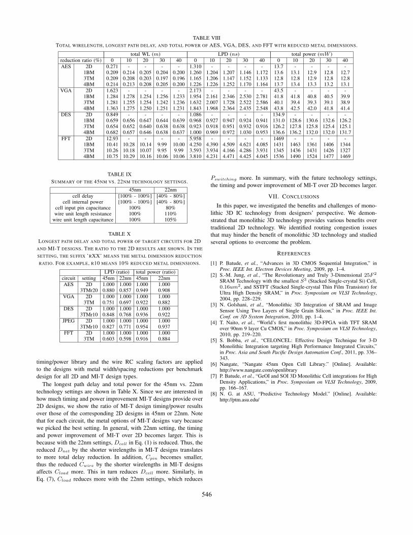
TABLE VIIITOTAL WIRELENGTH, LONGEST PATH DELAY, AND TOTAL POWER OF AES, VGA, DES, AND FFT WITH REDUCED METAL DIMENSIONS.
total WL (m) LPD (ns) total power (mW )reduction ratio (%) 0 10 20 30 40 0 10 20 30 40 0 10 20 30 40AES 2D 0.271 - - - - 1.310 - - - - 13.7 - - - -
1BM 0.209 0.214 0.205 0.204 0.200 1.260 1.204 1.207 1.146 1.172 13.6 13.1 12.9 12.8 12.73TM 0.209 0.208 0.203 0.197 0.196 1.165 1.206 1.147 1.152 1.133 12.8 12.8 12.9 12.8 12.84BM 0.214 0.213 0.208 0.205 0.200 1.226 1.226 1.252 1.170 1.164 13.7 13.4 13.3 13.2 13.1
VGA 2D 1.623 - - - - 2.173 - - - - 43.5 - - - -1BM 1.284 1.278 1.254 1.256 1.233 1.954 2.161 2.346 2.530 2.781 41.8 41.8 40.8 40.5 39.93TM 1.281 1.255 1.254 1.242 1.236 1.632 2.007 1.728 2.522 2.586 40.1 39.4 39.3 39.1 38.94BM 1.363 1.275 1.250 1.251 1.231 1.843 1.968 2.364 2.435 2.548 43.8 42.5 42.0 41.8 41.4
DES 2D 0.849 - - - - 1.086 - - - - 134.9 - - - -1BM 0.659 0.656 0.647 0.644 0.639 0.968 0.927 0.947 0.924 0.941 131.0 128.6 130.6 132.6 126.23TM 0.654 0.652 0.640 0.638 0.638 0.923 0.918 0.951 0.932 0.916 126.2 127.8 125.8 125.4 125.14BM 0.682 0.657 0.646 0.638 0.637 1.000 0.969 0.972 1.030 0.953 136.6 136.2 132.0 132.0 131.7
FFT 2D 12.93 - - - - 5.958 - - - - 1469 - - - -1BM 10.41 10.28 10.14 9.99 10.00 4.250 4.390 4.509 4.621 4.085 1431 1463 1361 1406 13443TM 10.26 10.18 10.07 9.95 9.99 3.593 3.934 4.166 4.286 3.931 1345 1436 1431 1426 13274BM 10.75 10.29 10.16 10.06 10.06 3.810 4.231 4.471 4.425 4.045 1536 1490 1524 1477 1469
TABLE IXSUMMARY OF THE 45NM VS. 22NM TECHNOLOGY SETTINGS.
45nm 22nmcell delay [100% - 100%] [40% - 80%]
cell internal power [100% - 100%] [40% - 80%]cell input pin capacitance 100% 80%wire unit length resistance 100% 110%
wire unit length capacitance 100% 105%
TABLE XLONGEST PATH DELAY AND TOTAL POWER OF TARGET CIRCUITS FOR 2D
AND MI-T DESIGNS. THE RATIO TO THE 2D RESULTS ARE SHOWN. IN THE
SETTING, THE SUFFIX ’RXX’ MEANS THE METAL DIMENSION REDUCTION
RATIO. FOR EXAMPLE, R10 MEANS 10% REDUCED METAL DIMENSIONS.
LPD (ratio) total power (ratio)circuit setting 45nm 22nm 45nm 22nmAES 2D 1.000 1.000 1.000 1.000
3TMr20 0.880 0.857 0.949 0.908VGA 2D 1.000 1.000 1.000 1.000
3TM 0.751 0.697 0.922 0.882DES 2D 1.000 1.000 1.000 1.000
3TMr10 0.848 0.768 0.936 0.922JPEG 2D 1.000 1.000 1.000 1.000
3TMr10 0.827 0.771 0.954 0.937FFT 2D 1.000 1.000 1.000 1.000
3TM 0.603 0.598 0.916 0.884
timing/power library and the wire RC scaling factors are appliedto the designs with metal width/spacing reductions per benchmarkdesign for all 2D and MI-T design types.
The longest path delay and total power for the 45nm vs. 22nmtechnology settings are shown in Table X. Since we are interested inhow much timing and power improvement MI-T designs provide over2D designs, we show the ratio of MI-T design timing/power resultsover those of the corresponding 2D designs in 45nm or 22nm. Notethat for each circuit, the metal options of MI-T designs vary becausewe picked the best setting. In general, with 22nm setting, the timingand power improvement of MI-T over 2D becomes larger. This isbecause with the 22nm settings, Dcell in Eq. (1) is reduced. Thus, thereduced Dnet by the shorter wirelengths in MI-T designs translatesto more total delay reduction. In addition, Cpin becomes smaller,thus the reduced Cwire by the shorter wirelengths in MI-T designsaffects Cload more. This in turn reduces Dcell more. Similarly, inEq. (7), Cload reduces more with the 22nm settings, which reduces
Pswitching more. In summary, with the future technology settings,the timing and power improvement of MI-T over 2D becomes larger.
VII. CONCLUSIONS
In this paper, we investigated the benefits and challenges of mono-lithic 3D IC technology from designers’ perspective. We demon-strated that monolithic 3D technology provides various benefits overtraditional 2D technology. We identified routing congestion issuesthat may hinder the benefit of monolithic 3D technology and studiedseveral options to overcome the problem.
REFERENCES
[1] P. Batude, et al., “Advances in 3D CMOS Sequential Integration,” inProc. IEEE Int. Electron Devices Meeting, 2009, pp. 1–4.
[2] S.-M. Jung, et al., “The Revolutionary and Truly 3-Dimensional 25F 2
SRAM Technology with the smallest S3 (Stacked Single-crystal Si) Cell,0.16um2, and SSTFT (Stacked Single-crystal Thin Film Transistor) forUltra High Density SRAM,” in Proc. Symposium on VLSI Technology,2004, pp. 228–229.
[3] N. Golshani, et al., “Monolithic 3D Integration of SRAM and ImageSensor Using Two Layers of Single Grain Silicon,” in Proc. IEEE Int.Conf. on 3D System Integration, 2010, pp. 1–4.
[4] T. Naito, et al., “World’s first monolithic 3D-FPGA with TFT SRAMover 90nm 9 layer Cu CMOS,” in Proc. Symposium on VLSI Technology,2010, pp. 219–220.
[5] S. Bobba, et al., “CELONCEL: Effective Design Technique for 3-DMonolithic Integration targeting High Performance Integrated Circuits,”in Proc. Asia and South Pacific Design Automation Conf., 2011, pp. 336–343.
[6] Nangate, “Nangate 45nm Open Cell Library.” [Online]. Available:http://www.nangate.com/openlibrary
[7] P. Batude, et al., “GeOI and SOI 3D Monolithic Cell integrations for HighDensity Applications,” in Proc. Symposium on VLSI Technology, 2009,pp. 166–167.
[8] N. G. at ASU, “Predictive Technology Model.” [Online]. Available:http://ptm.asu.edu/
546