trends in ic technology
TRANSCRIPT
8/10/2019 Trends in IC Technology
http://slidepdf.com/reader/full/trends-in-ic-technology 1/26
EE 311 Notes/Prof Saraswat Handout # 2
1
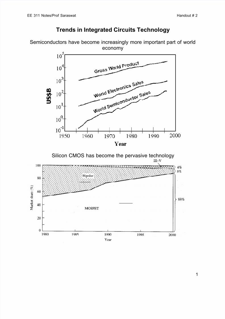
Trends in Integrated Circuits Technology
Semiconductors have become increasingly more important part of worldeconomy
Silicon CMOS has become the pervasive technology
8/10/2019 Trends in IC Technology
http://slidepdf.com/reader/full/trends-in-ic-technology 2/26
EE 311 Notes/Prof Saraswat Handout # 2
2
Year
T r a n s
i s t o r s o r
b i t s p e r c
h i p
M
i ni m um l i t h
o gr a
ph i c
f e a t ur e
si z e
( !m
)
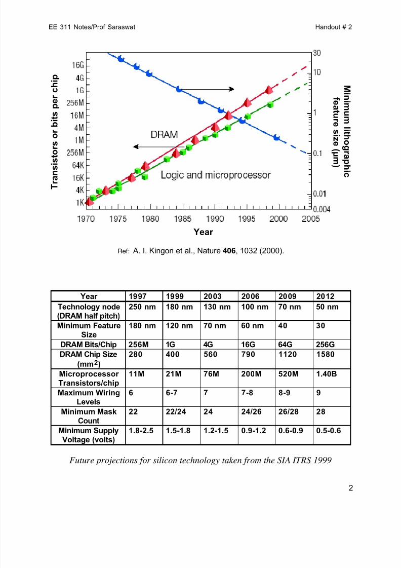
Ref: A. I. Kingon et al., Nature 406 , 1032 (2000).
Year 1997 1999 2003 2006 2009 2012Technology node(DRAM half pitch)
250 nm 180 nm 130 nm 100 nm 70 nm 50 nm
Minimum FeatureSize
180 nm 120 nm 70 nm 60 nm 40 30
DRAM Bits/Chip 256M 1G 4G 16G 64G 256GDRAM Chip Size
(mm 2 )280 400 560 790 1120 1580
Microprocessor Transistors/chip
11M 21M 76M 200M 520M 1.40B
Maximum WiringLevels
6 6-7 7 7-8 8-9 9
Minimum MaskCount
22 22/24 24 24/26 26/28 28
Minimum SupplyVoltage (volts)
1.8-2.5 1.5-1.8 1.2-1.5 0.9-1.2 0.6-0.9 0.5-0.6
Future projections for silicon technology taken from the SIA ITRS 1999
8/10/2019 Trends in IC Technology
http://slidepdf.com/reader/full/trends-in-ic-technology 3/26
EE 311 Notes/Prof Saraswat Handout # 2
3
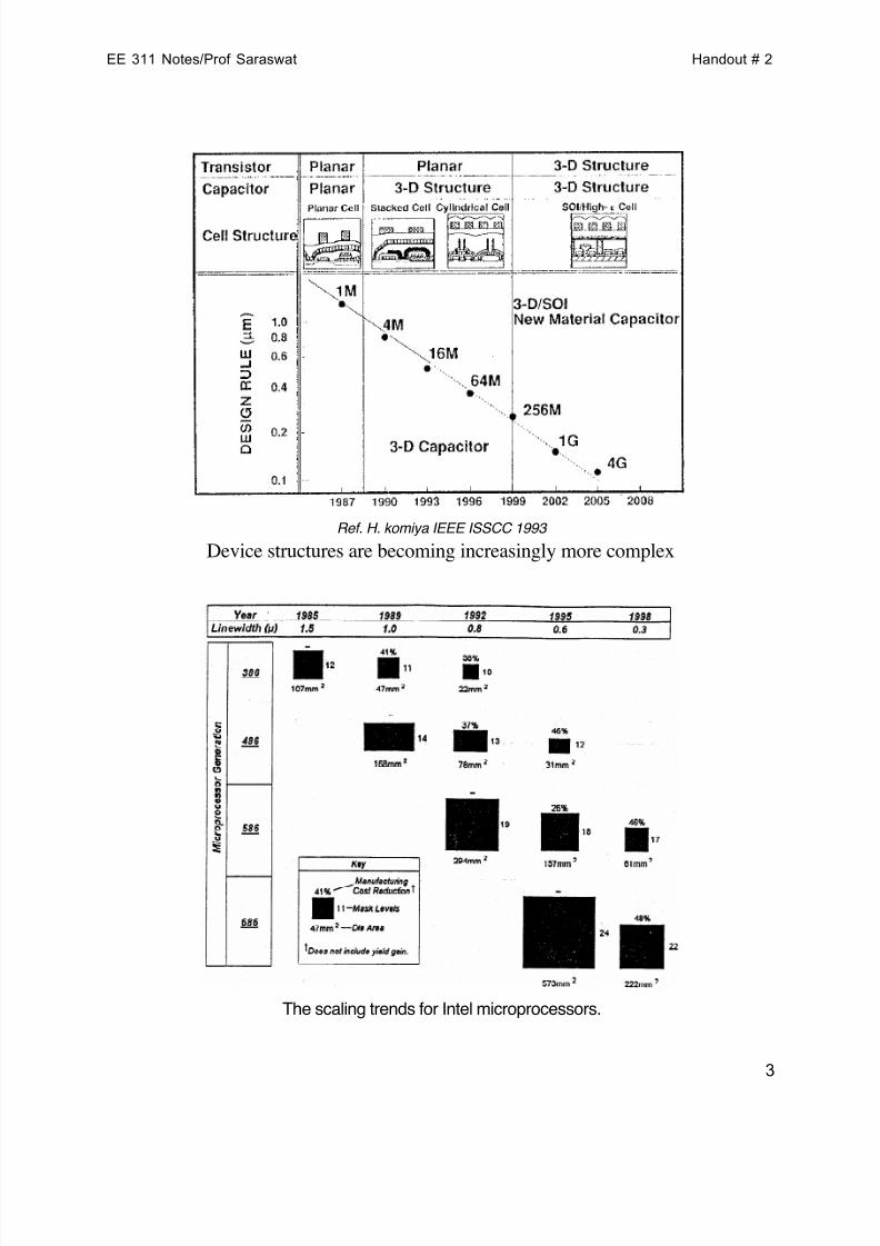
Ref. H. komiya IEEE ISSCC 1993
Device structures are becoming increasingly more complex
The scaling trends for Intel microprocessors.
8/10/2019 Trends in IC Technology
http://slidepdf.com/reader/full/trends-in-ic-technology 4/26
EE 311 Notes/Prof Saraswat Handout # 2
4
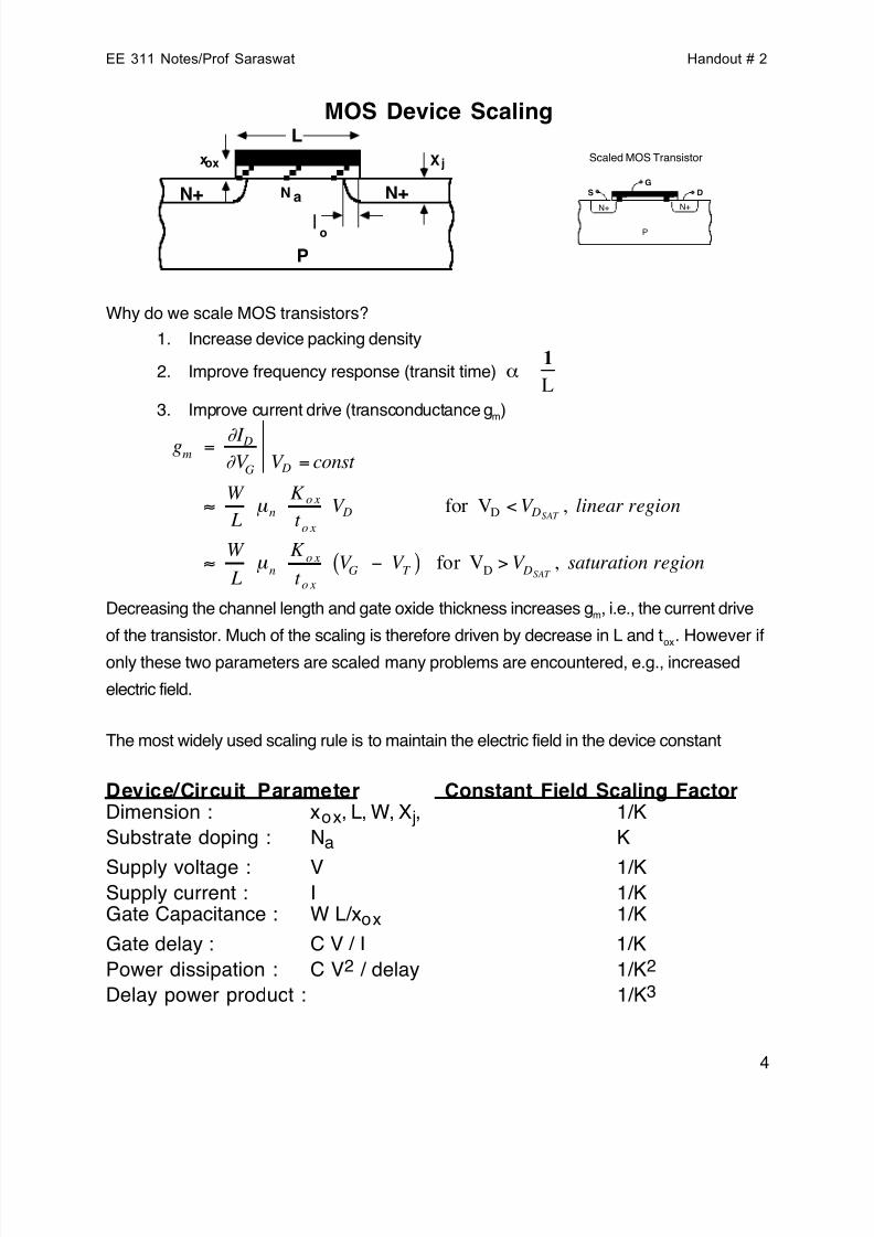
MOS Device Scaling
N a
P
N+N+
Lxox Xj
ol
Why do we scale MOS transistors?1. Increase device packing density
2. Improve frequency response (transit time) !1
L
3. Improve current drive (transconductance g m)
gm=
" I D" V G V D = const
# W L
µ nK o x
t o x
V D for V D < V DSAT , linear region
# W L
µ nK o x
t o x
V G $ V T ( ) for V D> V DSAT
, saturation region
Decreasing the channel length and gate oxide thickness increases g m, i.e., the current drive
of the transistor. Much of the scaling is therefore driven by decrease in L and t ox . However if
only these two parameters are scaled many problems are encountered, e.g., increased
electric field.
The most widely used scaling rule is to maintain the electric field in the device constant
Device/Circuit Parameter Constant Field Scaling FactorDimension : x ox , L, W, X j, 1/KSubstrate doping : N a K
Supply voltage : V 1/KSupply current : I 1/KGate Capacitance : W L/x ox 1/KGate delay : C V / I 1/KPower dissipation : C V 2 / delay 1/K 2
Delay power product : 1/K 3
P
N+N+
SG
D
Scaled MOS Transistor
8/10/2019 Trends in IC Technology
http://slidepdf.com/reader/full/trends-in-ic-technology 5/26
EE 311 Notes/Prof Saraswat Handout # 2
5
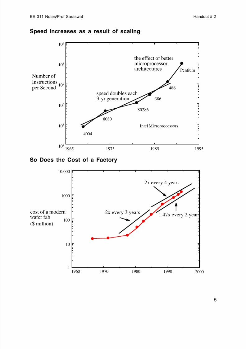
Speed increases as a result of scaling
So Does the Cost of a Factory
1965 1975 1985 199510 4
10 5
10 6
10 7
10 8
10 9
4004
8080
80286
386
486
Pentium
Intel Microprocessors
Number of Instructionsper Second
speed doubles each3-yr generation
the effect of bettermicroprocessorarchitectures
1960 1970 1980 1990 20001
10
100
1000
10,000
cost of a modernwafer fab($ million)
2x every 4 years
1.47x every 2 years2x every 3 years
8/10/2019 Trends in IC Technology
http://slidepdf.com/reader/full/trends-in-ic-technology 6/26
EE 311 Notes/Prof Saraswat Handout # 2
6
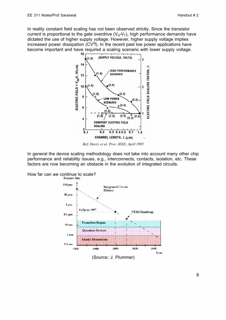
In reality constant field scaling has not been observed strictly. Since the transistor current is proportional to the gate overdrive (VG-VT), high performance demands havedictated the use of higher supply voltage. However, higher supply voltage impliesincreased power dissipation (CV 2f). In the recent past low power applications havebecome important and have required a scaling scenario with lower supply voltage.
Ref: Davri, et al. Proc. IEEE, April 1995
In general the device scaling methodology does not take into account many other chipperformance and reliability issues, e.g., interconnects, contacts, isolation, etc. Thesefactors are now becoming an obstacle in the evolution of integrated circuits.
How far can we continue to scale?
(Source: J. Plummer)
8/10/2019 Trends in IC Technology
http://slidepdf.com/reader/full/trends-in-ic-technology 7/26
EE 311 Notes/Prof Saraswat Handout # 2
7
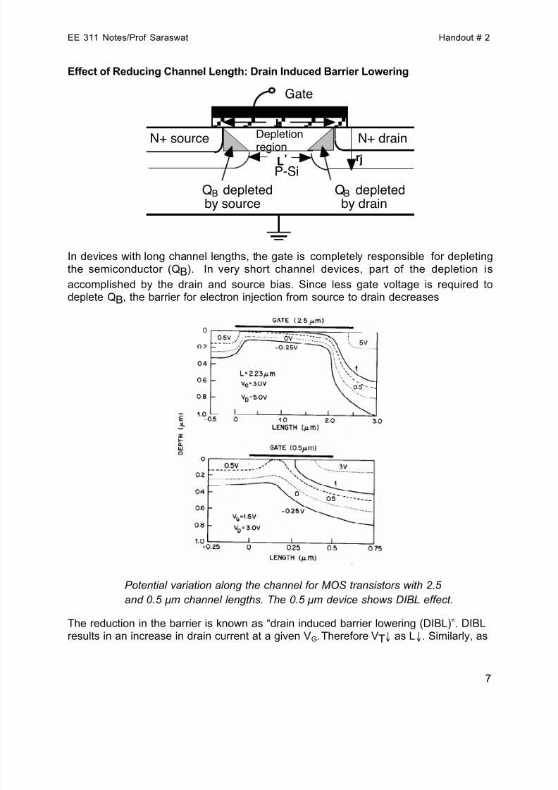
Effect of Reducing Channel Length: Drain Induced Barrier Lowering
Q depletedby source
Q depletedby drain
B B
N+ source N+ drain
Gate
P-Si
DepletionregionL’
L
rj
In devices with long channel lengths, the gate is completely responsible for depletingthe semiconductor (Q
B). In very short channel devices, part of the depletion is
accomplished by the drain and source bias. Since less gate voltage is required todeplete Q B, the barrier for electron injection from source to drain decreases
Potential variation along the channel for MOS transistors with 2.5 and 0.5 ! m channel lengths. The 0.5 ! m device shows DIBL effect.
The reduction in the barrier is known as “drain induced barrier lowering (DIBL)”. DIBLresults in an increase in drain current at a given V G. Therefore VT! as L ! . Similarly, as
8/10/2019 Trends in IC Technology
http://slidepdf.com/reader/full/trends-in-ic-technology 8/26
EE 311 Notes/Prof Saraswat Handout # 2
8
VD " , more QB is depleted by the drain bias, and hence I D" and VT! . This is
An approximate relation for threshold voltage due to DIBL is:
V T = V FB ! 2 "# F !
Q B
C ox
" 1 ! 1 +2 "W
r j
! 1$
%
& '
(
) "r j
L
*
+
,
-
.
/
To minimize the effect of DIBL:
• C ox should be increased, i.e., decrease gate oxide thickness.This results in increased control of the gate.
• Decrease junction depth (r j )
Scaling of gate oxide thickness and junction depth causes many other problems.
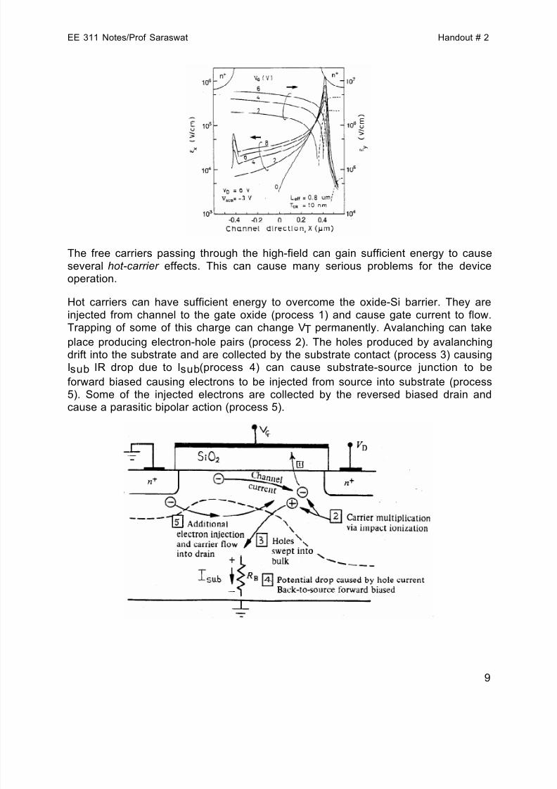
Hot Carrier Effects
For a reverse biased p-n junction discussion we remember that the maximum electricfield intensity is near the junction itself and it increases with the reverse bias.
! max =
2qN a (" i # VD )$ox
In the case of MOS transistor the potential drop along the channel is not uniform withmost of it across the reverse biased drain-substrate junction. Therefore the electricfield intensity is also non-uniform with the maximum occurring near the drain junction.
As the channel length is reduced the electric field intensity in the channel near thedrain increases more rapidly in comparison to the long channel case, even if V D isscaled, as # i does not scale.
8/10/2019 Trends in IC Technology
http://slidepdf.com/reader/full/trends-in-ic-technology 9/26
EE 311 Notes/Prof Saraswat Handout # 2
9
The free carriers passing through the high-field can gain sufficient energy to causeseveral hot-carrier effects. This can cause many serious problems for the deviceoperation.
Hot carriers can have sufficient energy to overcome the oxide-Si barrier. They areinjected from channel to the gate oxide (process 1) and cause gate current to flow.Trapping of some of this charge can change V T permanently. Avalanching can takeplace producing electron-hole pairs (process 2). The holes produced by avalanchingdrift into the substrate and are collected by the substrate contact (process 3) causingIsub IR drop due to Isub(process 4) can cause substrate-source junction to beforward biased causing electrons to be injected from source into substrate (process5). Some of the injected electrons are collected by the reversed biased drain andcause a parasitic bipolar action (process 5).
8/10/2019 Trends in IC Technology
http://slidepdf.com/reader/full/trends-in-ic-technology 10/26
EE 311 Notes/Prof Saraswat Handout # 2
10
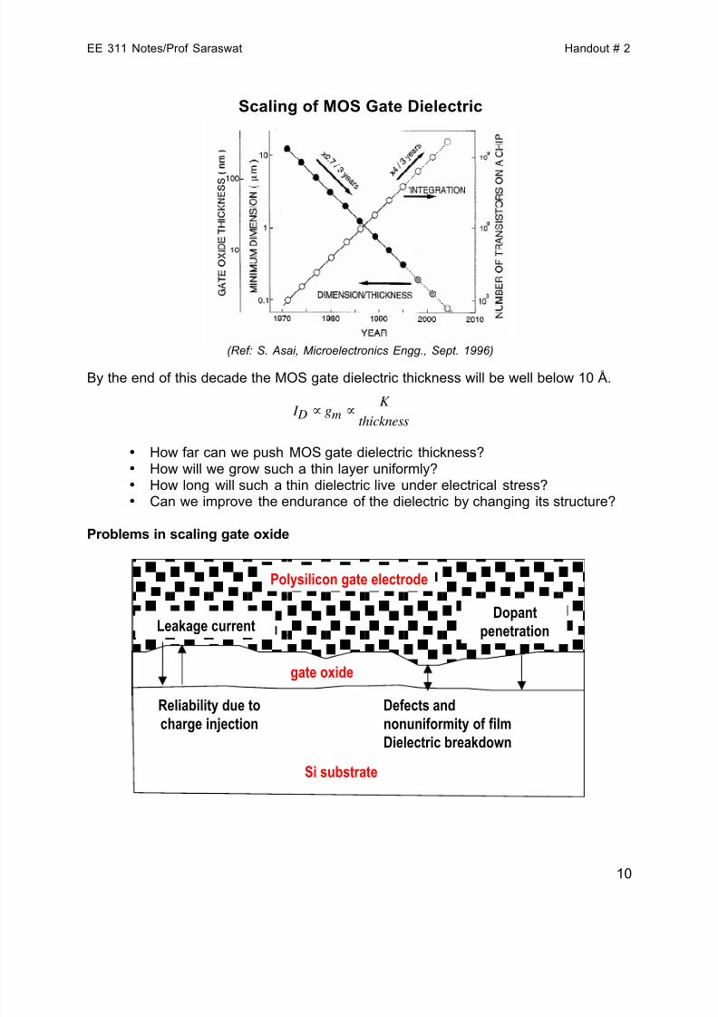
Scaling of MOS Gate Dielectric
(Ref: S. Asai, Microelectronics Engg., Sept. 1996)By the end of this decade the MOS gate dielectric thickness will be well below 10 Å.
• How far can we push MOS gate dielectric thickness?• How will we grow such a thin layer uniformly?• How long will such a thin dielectric live under electrical stress?• Can we improve the endurance of the dielectric by changing its structure?
Problems in scaling gate oxide
Defects andnonuniformity of filmDielectric breakdown
Reliability due tocharge injection
Si substrate
Polysilicon gate electrode
Dopantpenetration
gate oxide
Leakage current
I D ! gm !K
thickness
8/10/2019 Trends in IC Technology
http://slidepdf.com/reader/full/trends-in-ic-technology 11/26
EE 311 Notes/Prof Saraswat Handout # 2
11
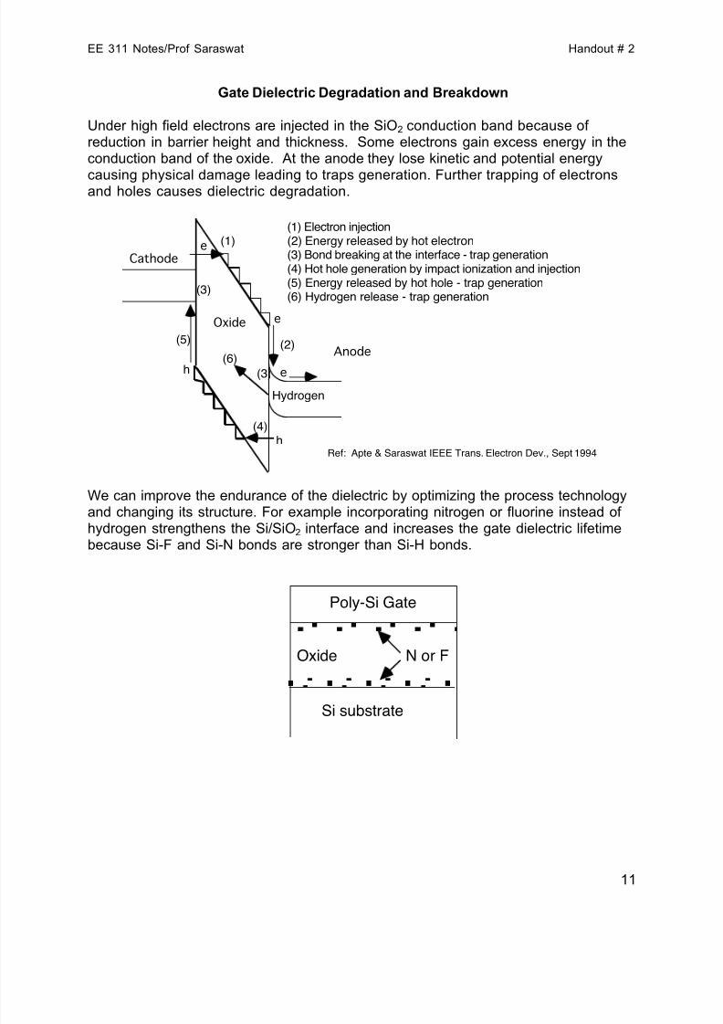
Gate Dielectric Degradation and Breakdown
Under high field electrons are injected in the SiO 2 conduction band because of reduction in barrier height and thickness. Some electrons gain excess energy in theconduction band of the oxide. At the anode they lose kinetic and potential energy
causing physical damage leading to traps generation. Further trapping of electronsand holes causes dielectric degradation.
eCathode
Oxide
Anode
h
(1)
(2)
(4)
(5)
(6)
Hydrogen
e
e
h
(1) Electron injection(2) Energy released by hot electron(3) Bond breaking at the interface - trap generation(4) Hot hole generation by impact ionization and injection(5) Energy released by hot hole - trap generation(6) Hydrogen release - trap generation
(3)
(3)
Ref: Apte & Saraswat IEEE Trans. Electron Dev., Sept 1994
We can improve the endurance of the dielectric by optimizing the process technologyand changing its structure. For example incorporating nitrogen or fluorine instead of hydrogen strengthens the Si/SiO 2 interface and increases the gate dielectric lifetimebecause Si-F and Si-N bonds are stronger than Si-H bonds.
Poly-Si Gate
Si substrate
Oxide N or F
8/10/2019 Trends in IC Technology
http://slidepdf.com/reader/full/trends-in-ic-technology 12/26
EE 311 Notes/Prof Saraswat Handout # 2
12
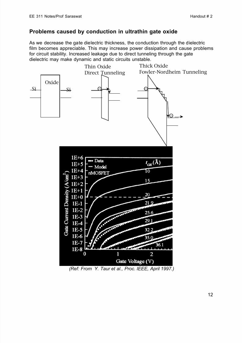
Problems caused by conduction in ultrathin gate oxide
As we decrease the gate dielectric thickness, the conduction through the dielectricfilm becomes appreciable. This may increase power dissipation and cause problemsfor circuit stability. Increased leakage due to direct tunneling through the gate
dielectric may make dynamic and static circuits unstable.
OxideSiSi
Thin OxideDirect Tunneling
Thick OxideFowler-Nordheim Tunneling
(Ref: From Y. Taur et al., Proc. IEEE, April 1997.)
8/10/2019 Trends in IC Technology
http://slidepdf.com/reader/full/trends-in-ic-technology 13/26
EE 311 Notes/Prof Saraswat Handout # 2
13
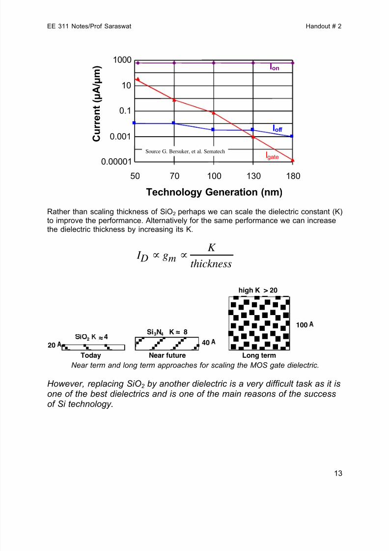
0.00001
0.001
0.1
10
1000
1801301007050
Technology Generation (nm)
C u r r e n
t ( !
A / ! m
)
Igate
Ioff
Ion
Source G. Bersuker, et al. Sematech
Rather than scaling thickness of SiO 2 perhaps we can scale the dielectric constant (K)to improve the performance. Alternatively for the same performance we can increasethe dielectric thickness by increasing its K.
20
100Si3N4 K ! 8
40Today Near future Long term
2 !
high K > 20
Near term and long term approaches for scaling the MOS gate dielectric.
However, replacing SiO 2 by another dielectric is a very difficult task as it isone of the best dielectrics and is one of the main reasons of the successof Si technology.
I D ! gm !K
thickness
8/10/2019 Trends in IC Technology
http://slidepdf.com/reader/full/trends-in-ic-technology 14/26
EE 311 Notes/Prof Saraswat Handout # 2
14
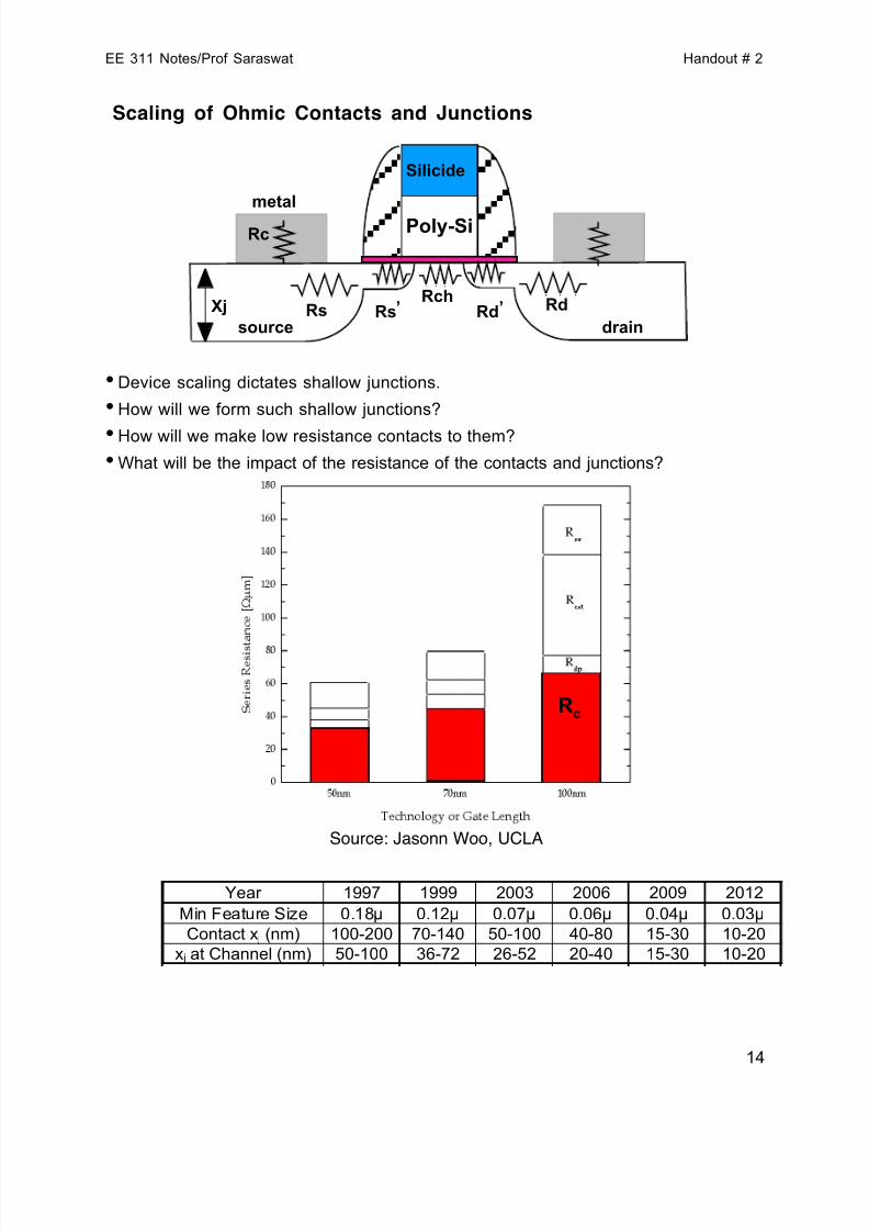
Scaling of Ohmic Contacts and Junctions
source
Rch
Silicide
Rc
Rsdrain
RdRd ’Rs ’
metal
Xj
Poly-Si
• Device scaling dictates shallow junctions.• How will we form such shallow junctions?
• How will we make low resistance contacts to them?• What will be the impact of the resistance of the contacts and junctions?
R c
Source: Jasonn Woo, UCLA
Year 1997 1999 2003 2006 2009 2012Min Feature Size 0.18 ! 0.12 ! 0.07 ! 0.06 ! 0.04 ! 0.03 !
Contact x j (nm) 100-200 70-140 50-100 40-80 15-30 10-20x j at Channel (nm) 50-100 36-72 26-52 20-40 15-30 10-20
8/10/2019 Trends in IC Technology
http://slidepdf.com/reader/full/trends-in-ic-technology 15/26
EE 311 Notes/Prof Saraswat Handout # 2
15
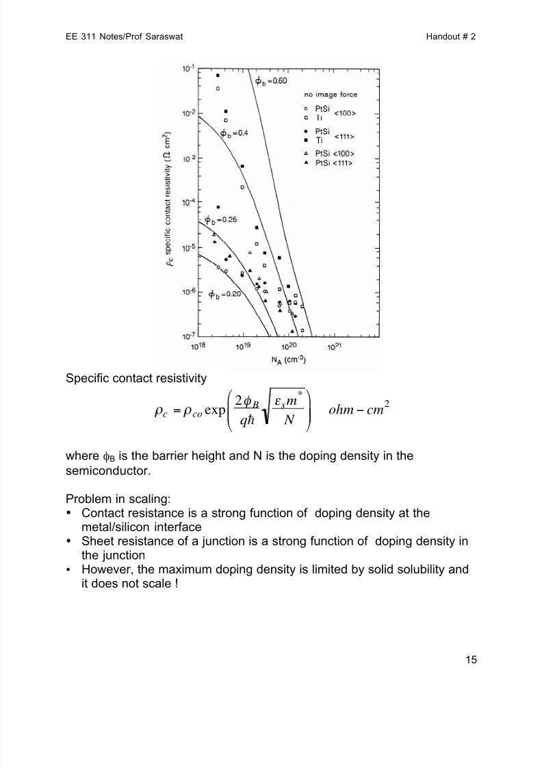
Specific contact resistivity
! c= ! co exp 2" B
qh# s m
*
N
$
%
& &
'
(
) ) ohm * cm 2
where #B is the barrier height and N is the doping density in thesemiconductor.
Problem in scaling:• Contact resistance is a strong function of doping density at the
metal/silicon interface• Sheet resistance of a junction is a strong function of doping density in
the junction• However, the maximum doping density is limited by solid solubility and
it does not scale !

8/10/2019 Trends in IC Technology
http://slidepdf.com/reader/full/trends-in-ic-technology 16/26
8/10/2019 Trends in IC Technology
http://slidepdf.com/reader/full/trends-in-ic-technology 17/26
EE 311 Notes/Prof Saraswat Handout # 2
17
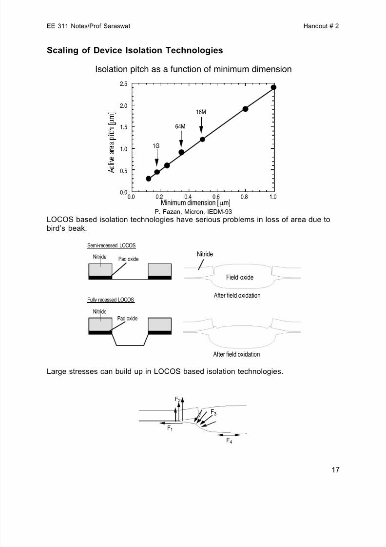
Scaling of Device Isolation Technologies
Isolation pitch as a function of minimum dimension
0.0 0.2 0.4 0.6 0.8 1.0Minimum dimension [µ m]
0.0
0.5
1.0
1.5
2.0
2.5
16M
64M
1G
P. Fazan, Micron, IEDM-93LOCOS based isolation technologies have serious problems in loss of area due tobird’s beak.
NitridePad oxide
Fully recessed LOCOS
Nitride Pad oxide
Semi-recessed LOCOS
Nitride
Field oxide
After eld oxidation
After eld oxidation
Large stresses can build up in LOCOS based isolation technologies.
F 4
F 1
F 2
F 3
8/10/2019 Trends in IC Technology
http://slidepdf.com/reader/full/trends-in-ic-technology 18/26
EE 311 Notes/Prof Saraswat Handout # 2
18
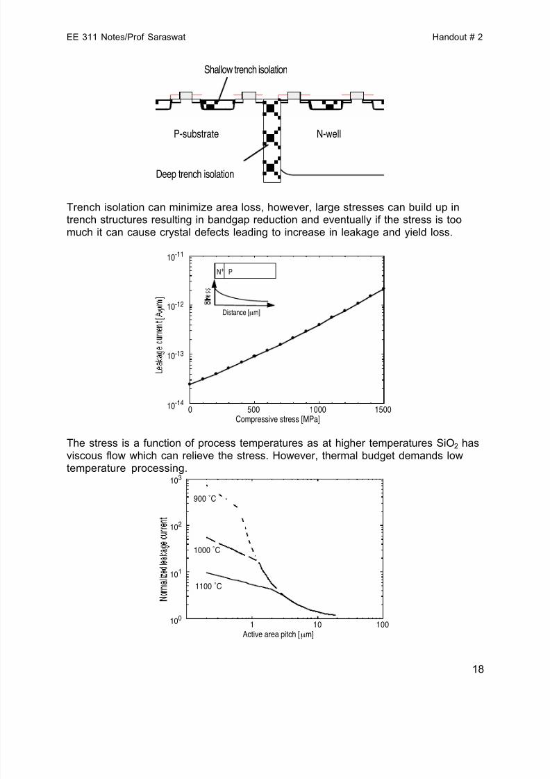
Deep trench isolation
N-wellP-substrate
Shallow trench isolation
Trench isolation can minimize area loss, however, large stresses can build up intrench structures resulting in bandgap reduction and eventually if the stress is toomuch it can cause crystal defects leading to increase in leakage and yield loss.
0 500 1000 1500Compressive stress [MPa]
10-14
10-13
10-12
10-11
Distance [µ m]
N+
P
The stress is a function of process temperatures as at higher temperatures SiO 2 hasviscous flow which can relieve the stress. However, thermal budget demands lowtemperature processing.
1 10 100Active area pitch [µ m]
100
101
102
103
900 ˚C
1000 ˚C
1100 ˚C
8/10/2019 Trends in IC Technology
http://slidepdf.com/reader/full/trends-in-ic-technology 19/26
EE 311 Notes/Prof Saraswat Handout # 2
19
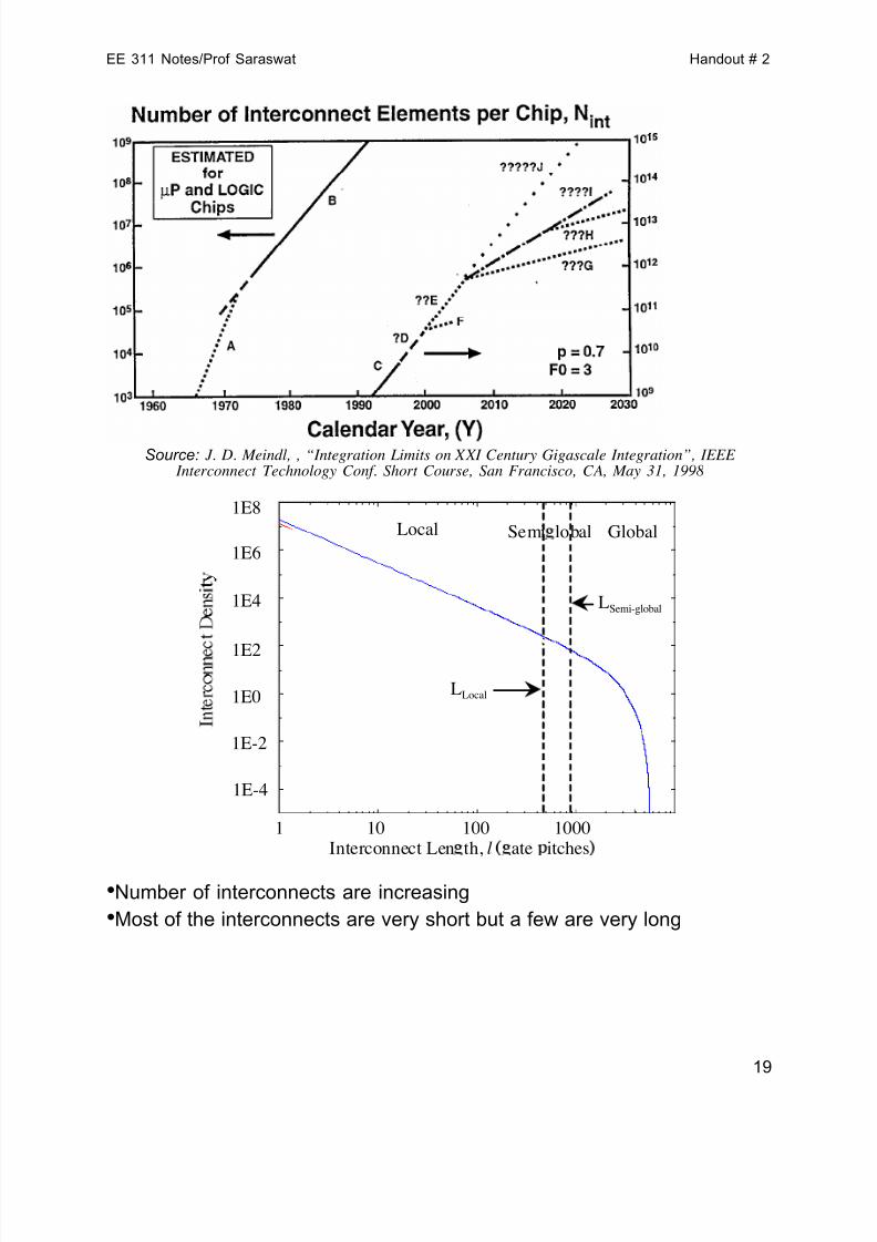
Source: J. D. Meindl, , “Integration Limits on XXI Century Gigascale Integration”, IEEE Interconnect Technology Conf. Short Course, San Francisco, CA, May 31, 1998
1 10 100 1000
1E-4
1E-2
1E0
1E2
1E4
1E6
1E8
Interconnect Len th, l ate itches
2D
3D
Local GlobalSemi lobal
LSemi-global
LLocal
•Number of interconnects are increasing•Most of the interconnects are very short but a few are very long
8/10/2019 Trends in IC Technology
http://slidepdf.com/reader/full/trends-in-ic-technology 20/26
EE 311 Notes/Prof Saraswat Handout # 2
20
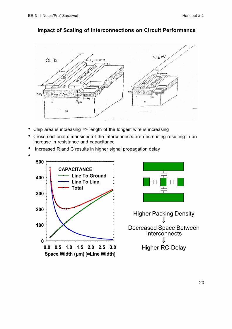
Impact of Scaling of Interconnections on Circuit Performance
• Chip area is increasing => length of the longest wire is increasing• Cross sectional dimensions of the interconnects are decreasing resulting in an
increase in resistance and capacitance• Increased R and C results in higher signal propagation delay•
Space Width ( ! m) [=Line Width]0.0 0.5 1.0 1.5 2.0 2.5 3.0
0
100
200
300
400
500
Line To GroundLine To LineTotal
CAPACITANCE
Higher Packing Density
Decreased Space BetweenInterconnects
Higher RC-Delay
8/10/2019 Trends in IC Technology
http://slidepdf.com/reader/full/trends-in-ic-technology 21/26
EE 311 Notes/Prof Saraswat Handout # 2
21
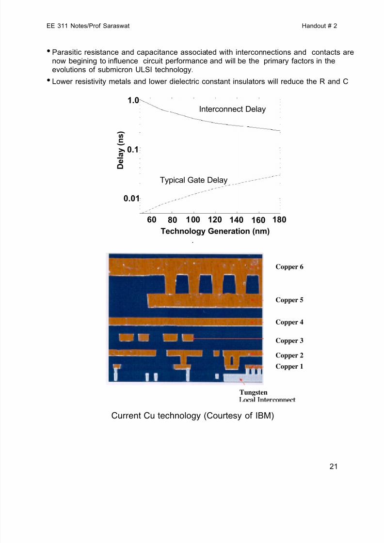
• Parasitic resistance and capacitance associated with interconnections and contacts arenow begining to influence circuit performance and will be the primary factors in theevolutions of submicron ULSI technology.
• Lower resistivity metals and lower dielectric constant insulators will reduce the R and C
80 100 120 140
0.1
0.01
Technology Generation (nm)
Typical Gate Delay
Interconnect Delay1.0
160 180
D e
l a y
( n s
)
60
.
Copper 6
Copper 1
Tungsten
Copper 3
Copper 5
Copper 4
Copper 2
Current Cu technology (Courtesy of IBM)
8/10/2019 Trends in IC Technology
http://slidepdf.com/reader/full/trends-in-ic-technology 22/26
EE 311 Notes/Prof Saraswat Handout # 2
22
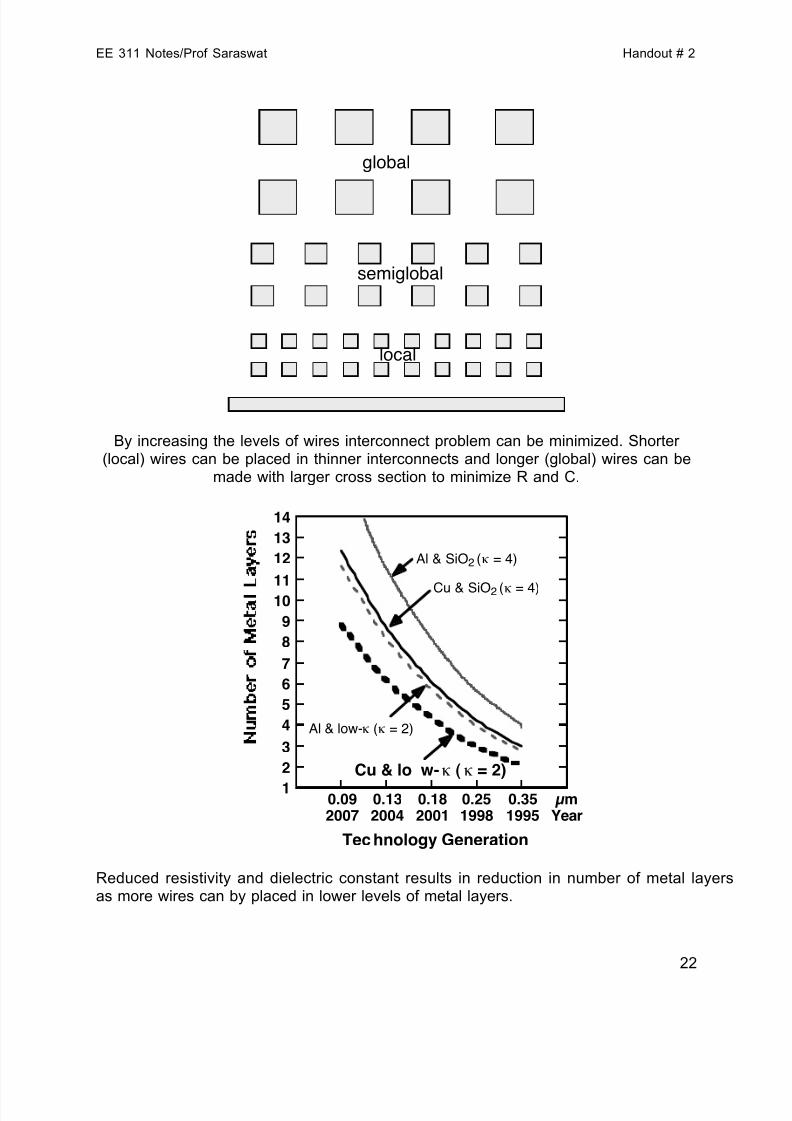
global
semiglobal
local
By increasing the levels of wires interconnect problem can be minimized. Shorter (local) wires can be placed in thinner interconnects and longer (global) wires can be
made with larger cross section to minimize R and C.
1
2
3
4
5
6
7
8
9
10
11
12
13
14
Al & SiO 2 ( ! = 4)
Cu & SiO 2 ( ! = 4)
Al & low- ! ( ! = 2)
Cu & lo w- ! ( ! = 2)
0.092007
0.132004
0.182001
0.251998
0.351995
Tec hnology Generation
µmYear
Reduced resistivity and dielectric constant results in reduction in number of metal layersas more wires can by placed in lower levels of metal layers.
8/10/2019 Trends in IC Technology
http://slidepdf.com/reader/full/trends-in-ic-technology 23/26
EE 311 Notes/Prof Saraswat Handout # 2
23
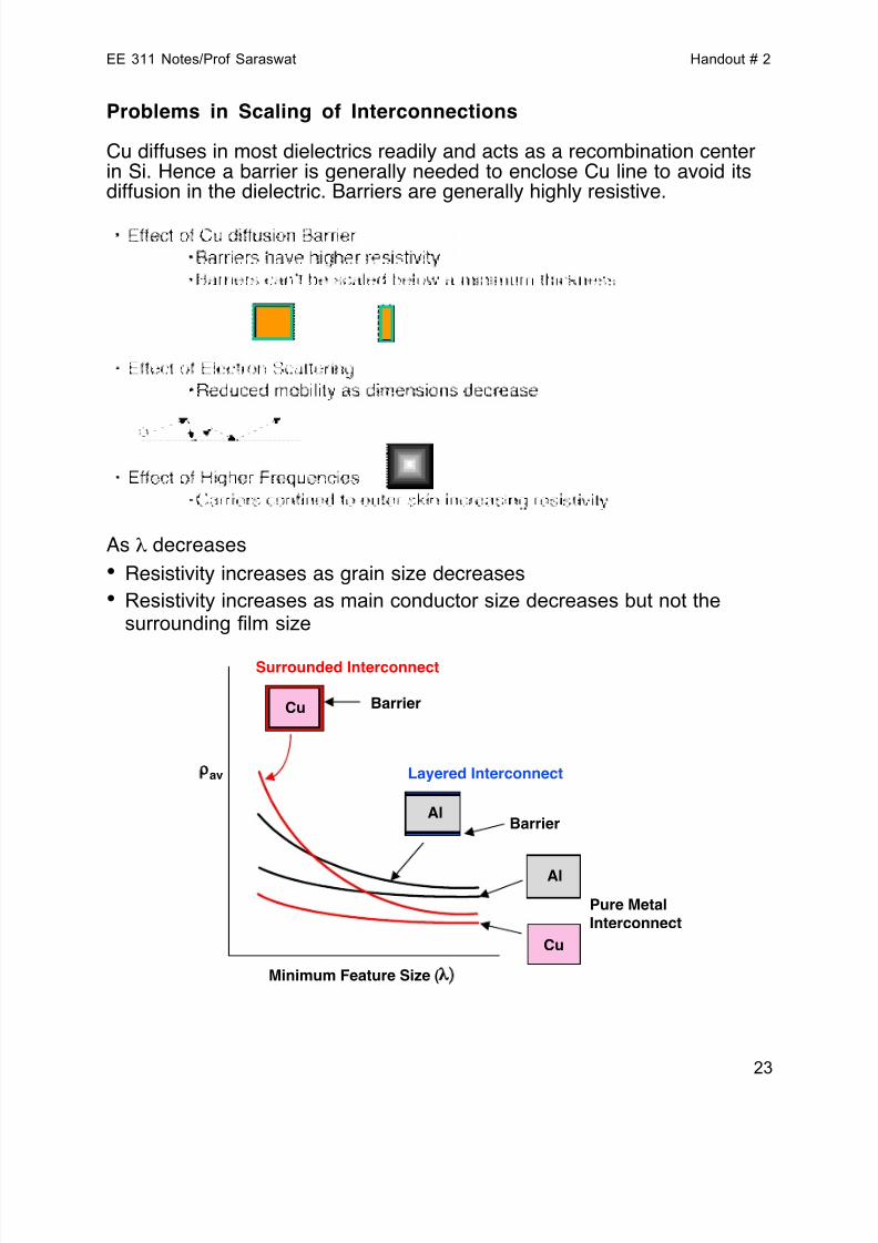
Problems in Scaling of Interconnections
Cu diffuses in most dielectrics readily and acts as a recombination centerin Si. Hence a barrier is generally needed to enclose Cu line to avoid itsdiffusion in the dielectric. Barriers are generally highly resistive.
As $ decreases• Resistivity increases as grain size decreases• Resistivity increases as main conductor size decreases but not the
surrounding film size
Pure MetalInterconnect
Layered Interconnect
Surrounded Interconnect
Al
Al
Cu
av
Minimum Feature Size (
Barrier
Barrier
Cu
8/10/2019 Trends in IC Technology
http://slidepdf.com/reader/full/trends-in-ic-technology 24/26
EE 311 Notes/Prof Saraswat Handout # 2
24
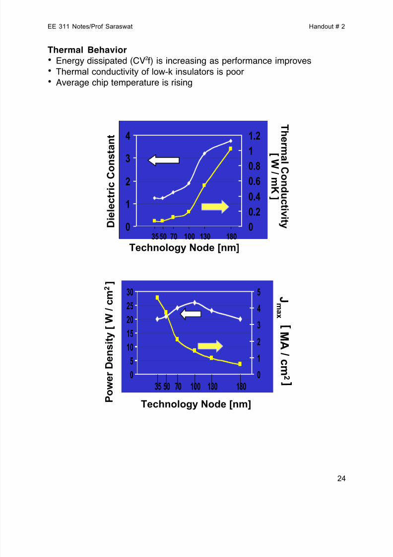
Thermal Behavior• Energy dissipated (CV 2f) is increasing as performance improves• Thermal conductivity of low-k insulators is poor • Average chip temperature is rising
35 50 70 130 1801000
1
2
3
4
0
0.20.4
0.6
0.8
1
1.2
Technology Node [nm]
D i e l e c t r i c
C o n s
t a n
tT h
er m al C on
d u c t i vi t y
[ W / m
K ]
35 50 70 100 130 180
0
5
10
15
20
2530
0
1
2
3
4
5
P o w e r
D e n s i t y
[ W
/ c m 2 ]
Technology Node [nm]
J m a x M A / c m
2
8/10/2019 Trends in IC Technology
http://slidepdf.com/reader/full/trends-in-ic-technology 25/26
EE 311 Notes/Prof Saraswat Handout # 2
25
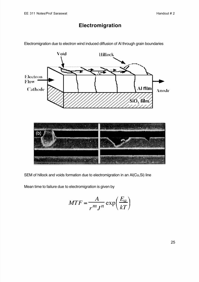
Electromigration
Electromigration due to electron wind induced diffusion of Al through grain boundaries
SEM of hillock and voids formation due to electromigration in an Al(Cu,Si) line
Mean time to failure due to electromigration is given by
MTF =
A
r m J n exp E akT
!
"
# $
%
&
8/10/2019 Trends in IC Technology
http://slidepdf.com/reader/full/trends-in-ic-technology 26/26
EE 311 Notes/Prof Saraswat Handout # 2
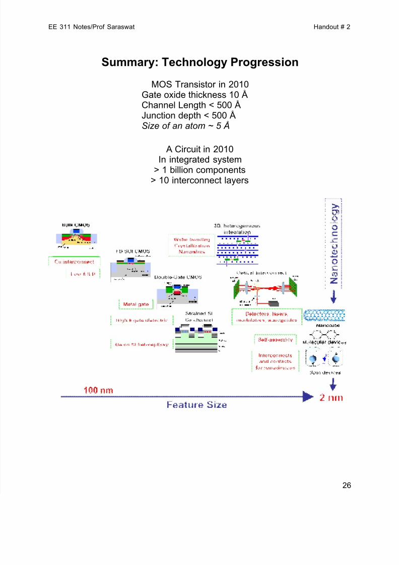
Summary: Technology Progression
MOS Transistor in 2010
Gate oxide thickness 10 ÅChannel Length < 500 ÅJunction depth < 500 ÅSize of an atom ~ 5 Å
A Circuit in 2010In integrated system
> 1 billion components> 10 interconnect layers