transport phenomena in tungsten lpcvd in a single-wafer ... · experimentally in a coldwall...
TRANSCRIPT
J. Electrochem. Soc., Vol. 138, No. 2, February 1991 �9 The Electrochemical Society, Inc. 509
Conclusions True global planarization over diverse patterns is not
likely to be achieved by spin application of an organic film followed by etchback, at least with materials common to the semiconductor industry. There exists a limiting pat- tern size above which a given material will not planarize in a single-film application.
A calculation method has been described for the deter- mination of long-range planarization quality over a diverse patter_~.. Results with a single film of photoresist have pro- vided the basis for pursuit of a two-film approach, making use of a block mask (PBM) and an overcoat layer for im- proved planarization. Difficulties with optimizing PBM design to achieve true global planarization are discussed, particularly with regard to complex patterns where simple line/space interpretations are difficult. Finally, an etch- back process with the ability to remove SiO~ and photore- sist at a 1:1 etch rate ratio has been described and used to complete the global planarization process sequence, demonstrating feasibility of the PBM/etchback approach for planarization over a diverse pattern.
Acknowledgment The authors would like to extend their appreciation to
Nancy Kenyon for her invaluable processing support.
Manuscript submitted March 23, 1990; revised manu- script received Aug. 27, 1990. This was Paper 208 pre- sented at the Los Angeles, CA, Meeting of the Society, May 7-12, 1989.
IBM assisted in meeting the publication costs of this ar- ticle.
REFERENCES 1. H. Hazuki and T. Moriya, VMIC Conf. Proc., 121 (1986).
2. L. Stillwagon, R. Larson, and G. Taylor, This Journal, 134, 2030 (1987).
3. H. Gokan, M. Mukainaru, and N. Endo, ibid., 135, 1019 (1988).
4. U. Gritsch, G. Higelin, G. Enders, and W. Muller, VMIC Conf. Proc., 69 (1988).
5. G. DeGraaf, A.L. Butler, and R. Penning DeVries, ibid., 357 (1988).
6. L. DeBruin and J. M. F. G. van Laarhoven, ibid., 404 (1988).
7. A. Schiltz and M. Pons, This Journal, 133, 178 (1986). 8. P. Riley and E. Castel, IEEE Trans. Semicond. Manu-
fact., 1, 154 (1988). 9. R.H. Wilson and P. A. Piacente, This Journal, 133, 981
(1986). 10. S. Fujii, M. Fukumoto, G. Fuse, and T. Ohzone, IEEE
Trans. Electron Devices, ED-35, 1829 (1988). 11. D. J. Sheldon, C. W. Gruenschlaeger, L. Kammerdiner,
N.B. Henis, P. Kelleher, and J .D. Haydan, IEEE Trans. Semicond. Manufact., 1, 140 (1988).
12. G. Fuse, H. Ogawa, K. Tateiwa, I. Nakao, S. Odanaka, M. Fukumoto, H. Iwasaki, and T. Ohzone, IEDM, 732 (1987).
13. T.H. Daubenspeck, C.W. Koburger, J .K. Debrosse, P.C. Sukanek, M. Armacost, P.C. Buschner, and J. A. Abernathey, Paper 208 presented at The Elec- trochemical Society Meeting, Los Angeles, CA, May 7-12, 1989.
14. B. Davari, C. Koburger, R. Schultz, T. Furukawa, J. Warnock, M. Jost, M. Kerbaugh, and J. Mauer, Sub- mitted to 1989 IEDM (Washington, DC).
15. R.H. Myers, "Response Surface Methodology," Ed- ward Bros., Inc., Ann Arbor, MI (1976).
16. A. S. Bergendahl, S. F. Bergeron, and D. L. Harmon, IBM J. Res. Dev., 26, 580 (1982).
17. P. L. deBruin and J. M. F. G. van Laarhoven, Proceed- ings of the IEEE VLSI Multilevel Interconnection Conference, p. 404, IEDM, Washington, DC (1988).
Transport Phenomena in Tungsten LPCVD in a Single-Wafer Reactor
C. R. Kleijn and C. J. Hoogendoorn Faculty of Applied Physics, Delft University of Technology, 2600 GA Delft, The Netherlands
A. Hasper, J. Holleman, and J. Middelhoek Faculty of Electrical Engineering, University of Twente, 7500 AE Enschede, The Netherlands
ABSTRACT
The influence of the WF~ concentration on the growth rate in tungsten LPCVD from WF6 and H2 has been studied both experimentally in a coldwall single-wafer reactor and with the use of a mathematical simulation model, predicting the gas flow, heat transfer, species transport, and chemical reactions in the reactor. Model predictions were in very good agree- ment with experimental growth rates and uniformities. The growth rate was found to be independent of the WF6 inlet pressure above a certain value Petit, whereas for WF6 inlet pressures below Pcr,t the growth rate decreases linearly with the WF6 inlet pressure. It is shown that this transition is due to mass-transfer limitations rather than a change in the reaction mechanism. The value of Petit depends on the reactor geometry and process conditions and may be obtained experimen- tally or from model simulations as presented in this study. It is shown that large concentration gradients may be present in CVD reactors, even at low reactant conversion rates, and that criteria for "gradientless" reactor operation based on conver- sion rates are incorrect. We propose a better criterion, based on the value of Pcrit. It is also shown that thermal diffusion phenomena in coldwall reactors are very important. As a result, WF6 concentrations at the wafer surface will al~vays be sig- nificantly lower than the inlet concentration.
In the last few years, the interest in the use of tungsten in multilevel metallization IC technology has grown consid- erably (1-5). Tungsten can be used as a diffusion barrier be- tween silicon and aluminum, as a shunting material on gate structures, and for the filling of vias and contact holes (6-8). The latter application requires deposition techniques capable of filling submicron, high aspect ratio holes with excellent conformality (high step coverage). Blanket tungsten LPCVD from H2-WF6, according to the overall re- action
WF6 + 3H2 ~ W + 6HF [1]
with subsequent backetching, is now widely used for this purpose (9-12). Recently, W-LPCVD from SiH4-WF6 has been discovered as an attractive alternative, offering many advantages such as a high and temperature-independent growth rate, smaller grain size, and less interaction with silicon (12-18). The poor step coverage, however, seems to make this process unsuitable for via filling in a blanket mode (19, 20). Like many other LPCVD processes, W-
Downloaded 22 Jun 2009 to 130.89.112.86. Redistribution subject to ECS license or copyright; see http://www.ecsdl.org/terms_use.jsp

510 J. Electrochem. Soc., Vol. 138, No. 2, February 1991 �9 The Electrochemical Society, Inc.
LPCVD from H2-WF6 has been developed in hotwall multi- ple-wafer-in-tube LPCVD reactors (21-25), but the use of coldwall (single-wafer) reactors is now more common (26-30). Coldwall single-wafer reactors offer several advan- tages over conventional hotwall systems, such as low par- ticle contamination, low WF6 consumption, suppression of gas phase reactions, efficient removal of reaction by-prod- ucts, excellent uniformity on large wafers, and easier wafer handling.
The deposition rate of tungsten from H2 and WF6 in LPCVD appears to be fully determined by surface chem- istry. For sufficiently high WF6 concentrations, the deposi- tion rate has been found to depend on the H2 partial pres- sure and the temperature, being independent of the WF6 partial pressure, according to
Rkin = Co [Pw~+] ~ [PH~] 1/2 e x p (-EA/RT) [2]
with EA --- 67-73 k J/tool (8, 21, 23, 26, 31). However, at very low WF6 partial pressures the growth rate has been found to decrease with decreasing WF6 concentration. This has been ascribed to mass-transfer limitations (27) and to changes in the reaction mechanism (32). In either case vari- ations in the WF6 concentration at the wafer surface will lead to nonuniform growth. Several other important quali- ties of tungsten films deposited through LPCVD from H2-WF6 seem to depend highly on the concentration, pres- sure, a n d t e m p e r a t u r e distributions in the reactor and at the wafer surface. Low temperatures, low WF6 concentra- tions, and low concentrations of reaction-products have been mentioned by several authors as factors favoring se- lective deposition (21, 24, 30, 33-35). Step coverage appears to be improved by high WF 6 partial pressures, low tem- peratures, and low H2 partial pressures (19, 20, 36, 37). En- croachment (undesired W growth in contact windows just underneath SiO2) has been found to decrease with decreas- ing temperature and WF6 pressure (38).
From the above it may be clear that it is important to have precise knowledge of the concentration and tempera- ture distributions in W-LPCVD reactors. These distribu- tions are mainly determined by hydrodynamics and trans- port phenomena in the gas mixture in the reactor. Especially in single-wafer reactors, where deposition rates have to be high in order to obtain sufficient throughput and reactor walls are eooled (leading to a high rate of reac- tant consumption and reaction-product formation and to strong thermal diffusion effects) significant concentration and temperature gradients will be present. Transport phe- nomena in CVD reactors may be studied in detail with the aid of mathematical simulation models describing the gas flow, the heat transfer and species diffusion, and the chem- ical reactions in the gas mixture. Such models have been developed successfully for various types of atmospheric pressure CVD reactors and for hotwall multiple-wafer LPCVD reactors (39, 40). Relatively few models for LPCVD in coldwall single-wafer reactors have been pub- lished. In a previous study we have presented a model for polysilicon LPCVD in a single-wafer reactor (4). It was shown that such a model should incorporate phenomena which have often been neglected in CVD modeling. Other models for LPCVD in single-wafer reactors (42-44) have been based on commercial ly available general-purpose computational fluid dynamics codes, which do not incor- porate several aspects which are relevant for accurate CVD modeling, such as mul t icomponent (thermal) diffu- sion and the influence of composit ion on the gas mixture properties.
It is the purpose of this paper to present a mathematical model for tungsten LPCVD from H2-WF6 in a coldwall sin- gle-wafer reactor and to validate the model predictions with experimental results. Several diagnostic tools may be used for the validation of CVD reactor simulation models. The most straightforward way is to compare predicted growth rates and growth uniformities with experimental observations. In tungsten LPCVD from H~-WF+, this method has limited value because of the insensitivity of the growth rate on the WF6 concentration (Eq. [2]). How- ever, the observed dependence of the growth rate on the WF6 concentration at very low WF6 concentrations may be
used to test a simulation model. A second possibility is the combination of a reactor simulation model with models for the prediction of microscopic film qualities and to com- pare predictions of these combined models with experi- mental results. Step coverage models, for example, predict a strong dependence of the step coverage on the WF6 con- centration at the pore mouth (19, 20, 36, 37). Now, by using the WF6 concentration at the wafer surface as calculated from the reactor model as a boundary condition for the step coverage model and comparing predicted step cover- ages with experimental observations, the combination of reactor model and step coverage model may be tested (20, 44, 45). A third possibility for the validation of a CVD reac- tor simulation model is the use of in situ laser diagnostic techniques for measuring temperatures and species con- centrations in the gas mixture and to compare these values to model predictions (46). This is a topic of present re- search. In this study, we have simulated tungsten LPCVD from H2 and WF6 in a coldwall single-wafer reactor and we have compared predicted growth rates and uniformities at high and low WF 6 concentrations to experimental results. Thus, we were able to test our simulation model. At the same t ime more insight was gained in the processes influ- encing the growth rate at low WF6 concentrations. This knowledge is important, because (i) for economic reasons it is interesting to use as little WF6 as possible, and (ii) for the accurate prediction of step coverage, precise knowl- edge of the mechanisms determining the growth rates at low WF6 concentrations is essential, since the WFG concen- tration inside trenches or contact holes may be very low.
Mathematical Model The mathematical model for the simulation of transport
phenomena and chemical reactions in a coldwall single- wafer reactor has been discussed in detail elsewhere (41). Here we will only give a brief description of the model and the implementat ion of the H2-WF6 process into the model, and we will amplify on some refinements which have re- cently been included. The model assumes steady-state conditions, laminar gas flow, and ideal gases, as well as the validity of the cont inuum approach. Since tungsten LPCVD from H2-WF6 is believed to be a fully heteroge- neous process, gas-phase reactions have not been taken into account.
Transport equations.--The gas flow and heat transfer in an N component gas mixture are described by the conti- nuity equation [3], the momentum balance equation or Navier-Stokes equation [4], and the energy equation [5] (symbols are explained in the List of Symbols)
v . (pv) = o [3]
V - ( p v v ) = V . ~(Vv+(Vv) T ) - ~ t x ( v - v ) - - V P + p g
[4]
N ) %V. (pvT)= V. (~VT)+ V - R T ~ ~ V(lnf~) [5]
The last term in Eq. [5] represents the Dufour effect (diffu- sion-thermo effect), which is the "reciprocal process" to the Soret effect (thermal diffusion effect). The first causes an energy flux as a result of concentration gradients in a gas mixture, whereas the second causes species diffusion fluxes as a result of temperature gradients. The Dufour ef- fect was not included in our previous model (41). In this study we have found that its influence on calculated tem- peratures is negligible (<0.1%) for the process conditions studied and we feel that this conclusion may be extrapo- lated to LPCVD processes in general.
The balance equation for gas species i can be written as
V. (pvtoi) = - V. (j~ + iT) (i = 1, N - 1) [6]
The ordinary (concentration) diffusion mass fluxes are ob- tained from the Stefan-Maxwell equations (in mass frac- tions and mass fluxes)
Downloaded 22 Jun 2009 to 130.89.112.86. Redistribution subject to ECS license or copyright; see http://www.ecsdl.org/terms_use.jsp

J. Electrochem. Soc., Vol. 138, No. 2, February 1991 �9 The Electrochemical Society, Inc. 511
M 1 c V(o i ~- r M) = - - ~ ~ (r j - r c) (i = 1, N - 1)
p j,~ mju~j [7]
S i n c e t h e m a s s f r ac t ions of t h e N spec ies m u s t s u m u p to 1 a n d t h e d i f fus ive m a s s f luxes m u s t s u m u p to 0, t h e r e are on ly N-1 i n d e p e n d e n t e q u a t i o n s of t he f o r m s of Eq. [6] a n d [7]. The t h e r m a l d i f fus ion m a s s f luxes are ca lcu la ted f rom
jT = _ DT V(ln T) (i = 1, N) [8]
Transport properties.--The t r a n s p o r t p r o p e r t i e s of t he i n d i v i d u a l gas spec ies a n d t h e b i n a r y o rd ina ry d i f fus ion coef f ic ien ts are ca l cu l a t ed f r o m C h a p m a n - E n s k o g g k ine t i c theory , a s s u m i n g L e n n a r d - J o n e s (6-12) i n t e r a c t i o n po ten- t ials (50). L e n n a r d - J o n e s p a r a m e t e r s for t he gas spec ies are g iven in Tab le I. S e m i e m p i r i c a l m i x t u r e ru les are u s e d for ca l cu l a t i ng t he t r a n s p o r t p r o p e r t i e s of t he gas m i x t u r e as a f u n c t i o n of p re s su re , t e m p e r a t u r e , a n d m i x t u r e compos i - t ion. P r e v i o u s l y (41) we h a v e u s e d a n a p p r o x i m a t e m e t h o d for c a l cu l a t i ng m u l t i c o m p o n e n t t h e r m a l d i f fus ion coeffi- c ients . B e c a u s e of t h e g rea t i m p o r t a n c e of t h e r m a l diffu- s ion p h e n o m e n a in gas mix tu re ' s c o n t a i n i n g H2 a n d WF~, we h a v e u s e d t h e e x a c t f o r m u l a t i o n s (Ref. (50) pp. 538-543) in th i s s tudy . Fo r a t yp i ca l gas m i x t u r e c o n s i s t i n g of 80% H2, 10% Ar, 5% WF6, a n d 5% H F at a t e m p e r a t u r e of 600 K, t he WF6 m u l t i c o m p o n e n t t h e r m a l d i f fus ion coeff ic ient ob- t a i n e d f r o m t h e a p p r o x i m a t e f o r m u l a t i o n was f o u n d to b e 45% lower c o m p a r e d to t he exac t fo rmula t ion . T h e calcula- t i on of m u l t i c o m p o n e n t t h e r m a l d i f fus ion coeff ic ients re- qu i res g rea t c o m p u t a t i o n a l ef for t a n d i nc r ea se s t he overa l l C P U t i m e n e e d e d b y a l m o s t 40%.
Boundary conditions.--Boundary c o n d i t i o n s m u s t b e speci f ied for t h e ve loc i ty vec tor , t h e t e m p e r a t u r e , a n d t h e spec ies c o n c e n t r a t i o n s in t h e inf low a n d t he out f low of t h e reac tor , on solid, n o n r e a c t i n g wal ls a n d o n t he wafe r su r face
In f low
Outf low
Sol id wal l s
Wafer su r face
n - v : V i n a n d n x v = 0 [9a]
T : Tin [9b]
r i = r m and n . (j~ + iT) = 0 [9C]
n . (Vpv) = 0 a n d n • v = 0 [10a]
n - V T = 0 [10b]
n . V~oi = 0 [ 1 0 c ]
v = 0 [ l l a ]
T = Twall or n . VT = 0 [ l i b ]
n . (j~ + jW) = 0 [ l l c ]
N
n . (pv) = R,ff ~ mi~/i a n d n • v = 0 [12a] ~=1
T = Twaf~ [125]
n . (ptoiv + j~ + iT) = mi~hR~ff [12c]
w i t h n a u n i t y v e c t o r n o r m a l to t he inf low/out f low o p e n i n g or wal l /wafer surface .
Surface reaction and mass-transfer-limited g r o w t h . - For suf f ic ien t ly h i g h WF8 c o n c e n t r a t i o n s , t he r eac t i on ra te of t h e su r face r e a c t i o n is g i v e n b y Eq. [2]. A t ve ry low WF6 c o n c e n t r a t i o n s , h o w e v e r , t he overa l l g r o w t h ra te c a n n o t r e m a i n i n d e p e n d e n t of t h e WF6 p ressu re , b e c a u s e of mass - t r a n s f e r l imi ta t ions . I t is a lso pos s ib l e t h a t t h e r eac t i on ra te c h a n g e s f r o m zero o rde r to n o n z e r o o rde r in WF6 at low WF6 c o n c e n t r a t i o n s . V a n de r P u t t e (32), for example , as- s u m e d t he r e a c t i o n to b e 1/6 o rde r in WF6 at low WF6 con- cen t r a t ions . In t h i s s tudy , we h a v e a s s u m e d t h a t t he ra te of t he h e t e r o g e n e o u s r eac t i on r e m a i n s zero o rde r in WF6
Table 1. Lennard-Jones Parameters
m ~r e/k Gas (kg. mol -~) (A) (K) Reference
H2 0.002016 2.827 59.7 (47) WF6 0.29784 5.21 338 (48, 49) ~ HF 0.02001 3.138 330 (47) Ar 0.039944 3.542 93.3 (47)
a Estimated from critical parameters, using Tc = 443 K, TB - 290.2 K, Vc = 227.9 cm3/mol, VB = 86.63 cm3/mol, and Pc = 42.7 bar.
d o w n to v e r y low p res su res . Th i s a s s u m p t i o n is s u p p o r t e d b y our e x p e r i m e n t a l g r o w t h ra te m e a s u r e m e n t s , as will b e d i s c u s s e d later. T h e overa l l g r o w t h ra te is d e s c r i b e d b y a m e c h a n i s m t h a t c o n s i d e r s t he s e q u e n t i a l p roces se s of gas- p h a s e d i f fus ion of r e a c t a n t s to t he wafe r su r face a n d a zero o rde r h e t e r o g e n e o u s reac t ion , as was d o n e b y Ulac ia et al. (42)
1 1 1 3 - + + - - [13]
Reff Rkm RD,WF s RD,H2
Here, Reff is t h e d e p o s i t i o n rate , Rkin is t h e r eac t i on ra te de- t e r m i n e d b y t h e h e t e r o g e n e o u s r eac t i on k ine t ics , a n d RD, i is t he m a x i m u m d i f fus ion f lux of spec ies i to t h e wafe r sur- face. T h r o u g h Eq. [13], t h e s lowes t of t h e t h r e e m e c h a n - isms, d i f fus ion of WF8 to t h e wafer , d i f fus ion of H2 to t he wafer , a n d h e t e r o g e n e o u s r eac t i on at t h e wafe r surface , de- t e r m i n e s t h e d e p o s i t i o n rate. Usua l l y a large excess of H2 is used , so RD.H2 > > RD.WF 6. B a s e d on t he e x t e n s i v e se t of ex- p e r i m e n t a l g r o w t h ra t e s p u b l i s h e d b y B r o a d b e n t a n d Ra- mi l l e r (23), Rki n w a s ca lcu la t ed f r o m Eq. [2], u s i n g
co = 1.7 mo l �9 P a -'/2 �9 m -2 �9 s -~ [14]
EA = 69 k J - mo1-1 - K -1
w i t h a s ta t i s t ica l e r ro r of -+ 0.5 m o l - P a 2/2. m 2. s ' (95%) in t h e v a l u e of co a t f ixed EA. The m a x i m u m mole flux of spe- cies i to t h e wafe r su r face RD, i is ca l cu la t ed f rom the maxi - m u m d i f fus ive f lux f rom t h e first d i sc re t i za t ion gr id p o i n t to t h e wafe r su r face as
1 ple~o)~ R D , i - - [15]
mi h
w h e r e t h e s u p e r s c r i p t 1 d e n o t e s t h e v a l u e in t he f irst gr id p o i n t n e x t to t h e wafe r surface, h is t h e d i s t a n c e f rom the wafe r su r face to th i s p o i n t (1 m m on t h e s t a n d a r d grid), a n d Di is a n e f fec t ive o r d i n a r y d i f fus ion coeff ic ient for spe- cies i in t h e gas m i x t u r e , ca l cu la t ed f rom
jc Di - [16]
pVco~
No te t h a t Eq. [15] ha s b e e n b a s e d on t h e fact t h a t t he spe- cies d i f fus ion to t h e wafe r su r face r eaches a m a x i m u m w h e n t h e spec ies c o n c e n t r a t i o n at t he wafe r su r face be- c o m e s zero. S i n c e D w -~ 0 for toi ~ 0, Eq. [15] does no t in- c lude a t h e r m a l d i f fus ion f lux te rm.
Numerical solution method.--The a b o v e set of par t ia l dif- fe ren t ia l e q u a t i o n s w i t h b o u n d a r y c o n d i t i o n s is so lved in t w o - d i m e n s i o n a l , a x i s y m m e t r i c form, u s i n g a cont ro l - v o l u m e - b a s e d f ini te d i f f e rence m e t h o d (41, 51). The equa- t ions are d i sc re t i zed on a n o n u n i f o r m , cy l indr ica l gr id a n d are so lved i te ra t ive ly , u s i n g a T D M A l ine-by- l ine m e t h o d . F o r m o s t ca l cu la t ions a 35 x 35 gr id was used. Gr id inde- p e n d e n c e was c h e c k e d o n 50 • 50 a n d 70 • 70 gr ids for s o m e r e p r e s e n t a t i v e s i tua t ions . The ca l cu la t ed d e p o s i t i o n ra tes a n d spec ies c o n c e n t r a t i o n s at t h e wafe r su r face ob- t a i n e d o n t h e s e f ine gr ids d i f fe red less t h a n 3% f rom t h o s e o b t a i n e d on t h e s t a n d a r d grid. T h r e e c o n v e r g e n c e cr i ter ia we re used : (i) t h e e r ror in t h e g loba l m a s s b a l a n c e for t he to ta l flow, <10-2%, (ii) t h e e r ro r in t h e g lobal m a s s b a l a n c e for e ach of t he gas species , <1%, a n d (iii) t h e r e s idua l s of t he e q u a t i o n s ( abso lu t e va lues , s u m m e d over t he grid, nor-
Downloaded 22 Jun 2009 to 130.89.112.86. Redistribution subject to ECS license or copyright; see http://www.ecsdl.org/terms_use.jsp
512 J. Electrochem. Sac., Vol. 138, No. 2, February 1991 �9 The Electrochemical Society, Inc.
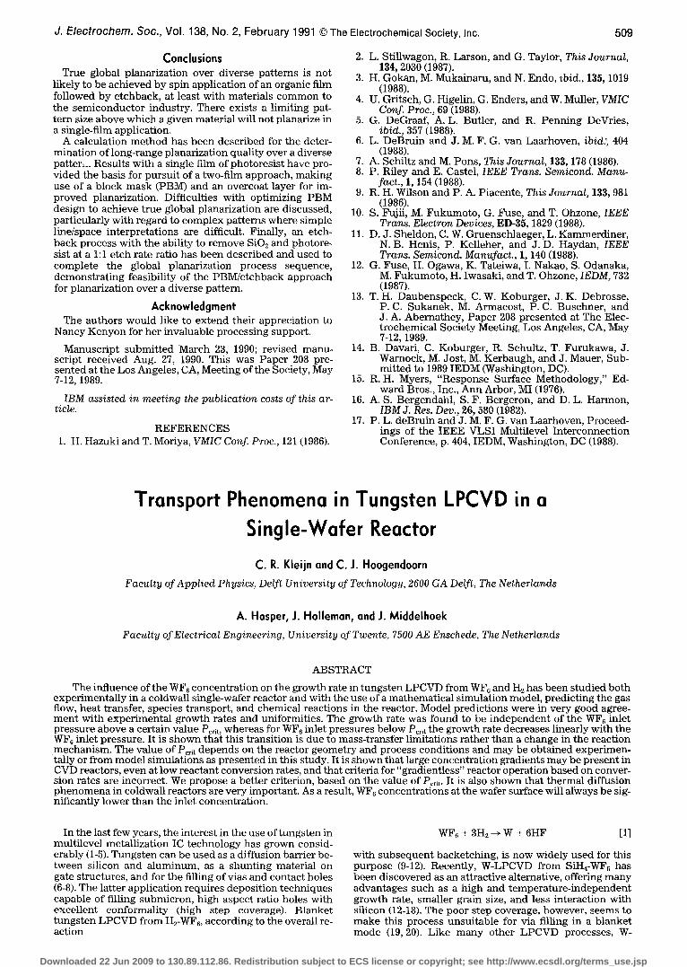
PYROMETER [~ QUARTZ WINDOW COOLED
3"WA ER I ', I I 8" WAFER ~ - ~ . ~ - . . ~ l S U S T C E G T ~ [ [
ELEMENT I,I couPLES Ar-n GAS OUTLET TO PUMP
IALVES ==BE
E H2-mfc
Ar H
TO PUMP
1 WF 6 -rr
~ NEEDLE VALVE
WE6
Fig. 1. Schematic representation of the reactor chamber with gas lines.
malized by a characteristic value for the variable and nor- malized by the number of grid points), <10 .8 . Changes of less than 1% in the calculated deposition rates and wafer surface concentrations occurred when these criteria were reduced to 10 -~, 10 1, and 10-7%. All calculations were car- ried out on a HP 9000-835 minicomputer. To reach a con- verged solution on the standard grid, ca. 5000 iterations are needed taking 3.6s per iteration.
Experimental Tungsten LPCVD growth rates were studied experimen-
tally in a loadlocked ASM coldwall single-wafer reactor which is designed for handling 8 in. wafers. In the present experiments, 3 in. p-type 10 ~ - cm (100) wafers were used which were placed in the center of an 8 in. SiO~-coated car- rier wafer. A schematic sketch of the reactor and gas lines is presented in Fig. 1. The walls of the cylindric stainless steel reactor chamber are water cooled. The wafer is placed facing upward on a 0.24m diam graphite susceptor, which is placed on top of a quartz dome. The susceptor is heated indirectly by a resistance heating element, which is placed up against the inside upper wall of the quartz dome. The parts of the dome outside the susceptor are protected from heating up through radiation shields and remain rela- tively cold. Gases are introduced radially into a 0.20m diam gas injection tube, which is positioned perpendicu- larly above the wafer surface. The purity of the gas sources (WF6, Ar, H2) employed in this study was 99.999% accord- ing to manufacturer 's specifications. The upper wall of the reactor, opposite to the wafer surface, consists of a water- cooled quartz window, allowing the silicon wafer surface temperature to be measured using a dual-wavelength py-
rometer. In this way, the wafer temperature was known at the starting of the deposition with an accuracy of -+ 5K. During the deposition, the susceptor temperature as meas- ured by a series of thermocouples was kept constant. Since we wanted to run growth experiments at extremely low WF6 supplies, special attention was given to the cali- bration of the WF6 flow. Very low flows were realized by putting a needle vFive in se:ies with the mass flow con- troller (Fig. 1). Calibration was done by measuring the pressure rise in the known constant volume of the reactor with the outlet valves closed. Thus, we were able to adjust flows down to 0.4 sccm with an accuracy of + 0.05 sccm. Immediately before loading the wafer into the reactor, a HF (1:100) dip of 30s was applied. Deposition was stopped immediately at the moment that selectivity was lost at the susceptor and the carrier wafer, as could easily be ob- served visually by looking through the quartz window op- posite to the susceptor. Layer thicknesses were measured by weight increase, with an accuracy of -+ 0.05 mg, and by using a profilometer and were corrected for the thickness of the initial, silicon-reduced, tungsten layer. Using the first method, the overall thickness could be measured, from which the wafer average growth rate could be deter- mined with an accuracy of -+ 20 ~Jmin. The profilometer measured the local thickness, thus allowing determination of growth rate uniformities. One has to realize, however, that profilometer measurements suffer from surface roughness. SEM observations showed that the effective roughness may be in the order of 10% of the total layer thickness for hydrogen-reduced LPCVD tungsten films.
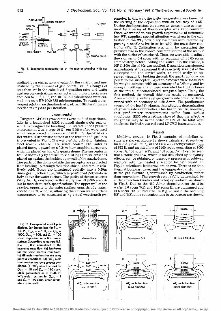
Results Modeling results .--In Fig. 2 examples of modeling re-
sults are shown. Figure 2a shows calculated streamlines for a total pressure Ptot of 133 Pa, a wafer temperature Twafe r of 673 K, and an inlet flow of 1200 sccm, consisting of 1000 sccm H~, 100 sccm WF6, and 100 sccm Ar. It can be seen that a stable gas flow, which is not disturbed by buoyancy effects, can be obtained at these low pressures in coldwall reactors with the heated susceptor facing upward. In Fig. 2b calculated isotherms are shown. There is no thin thermal boundary layer and the temperature distribution in the gas mixture is determined by conduction, rather than convection. The g rowth rate is fully determined by surface reaction kinetics and is highly uniform, as shown in Fig. 3. Due to the 460 /~Jmin deposition on the 8 in. wafer, 3.6 sccm WF6 and 10.8 sccm H2 are consumed and 21.6 sccm HF is produced. In Fig. 2c and d the resulting HF and WF6 mole concentrations in the reactor are shown.
Fig. 2. Examples of model pre- dictions. (a) Streamlines for Ptot = 133 Pa, Twof~, = 673 K, and Q,2 = 1000, QWF6 = 100, and QAr = 100 sccm. Deposition on a 8 in. wafer surface. Streamline values are 0.1, 0 . 2 , . . . , 0.9, normalized at the incoming mass flow. (b) Isotherms for the same process conditions. (c) HF mole fractions for the same process conditions. (d) WF6 mole fractions for the same process con- ditions. (e) WF6 mole fractions for QwF 6 = I 0 and QAr = 190 scem, other parameters as in (a-d). (f) WF 6 mole fractions for Qwr6 = 1 and QA, = 199 sccm, other param- eters as in (a-d).
art
,4_ ~---o.og--~ ~ _
/ WF 6 mole fraction / ~. (inlet 0.o83) .../
F
i s o t h e r m s (K)
- o.o09 ~% F-
f " O.OO4----~-'~
WF 6 mole fraction (inlet 0.0083)
1
1
I
HF mole fraction I
I
_____p~ o . o o o . - N _ _ - -
f ~ - o . o o o 2 ~
WF e mole fraction
(inlet 0.OO083)
Downloaded 22 Jun 2009 to 130.89.112.86. Redistribution subject to ECS license or copyright; see http://www.ecsdl.org/terms_use.jsp
J. Electrochem. Soc., Vol. 138, No. 2, February 1991 �9 The Electrochemical Society, Inc. 513
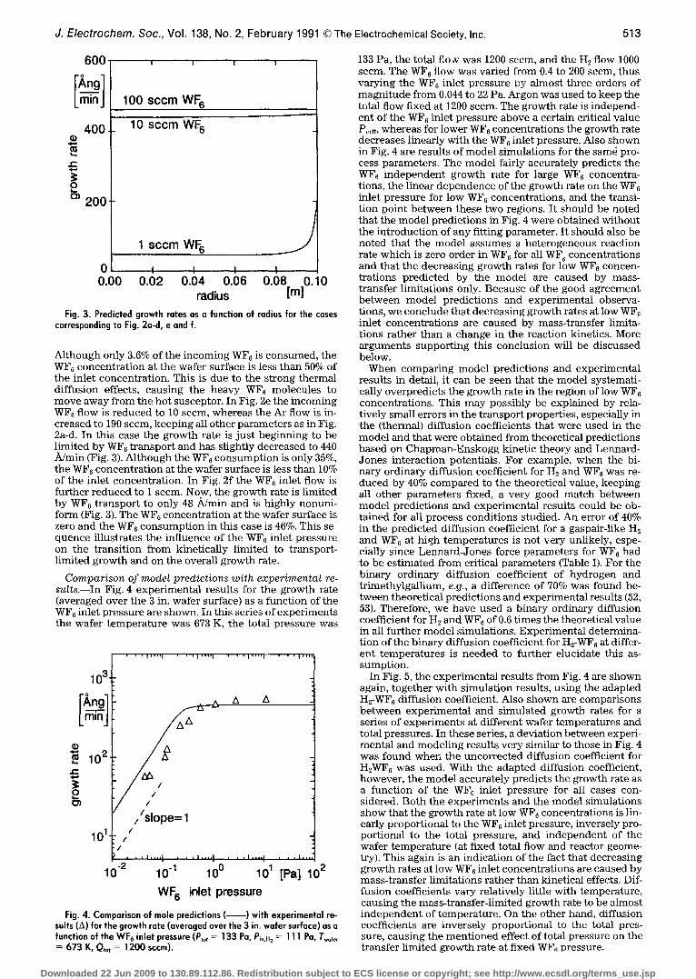
600
Lminj
400.
9 m 2 0 0
100 sccm WF 6
10 sccm WF 6
1 sccm WF 6
0 ; i i i 0.00 0.02 0.04 0.06 0.08 0.10
radius [m]
Fig. 3. Predicted growth rates as a function of radius for the cases corresponding to Fig. 2a-d, e and f.
Although only 3.6% of the incoming WF6 is consumed, the WF6 concentration at the wafer surface is less than 50% of the inlet concentration. This is due to the strong thermal diffusion effects, causing the heavy WF6 molecules to move away from the hot susceptor. In Fig. 2e the incoming WF6 flow is reduced to 10 sccm, whereas the Ar flow is in- creased to 190 sccm, keeping all other parameters as in Fig. 2a-d. In this case the growth rate is just beginning to be limited by WF6 transport and has slightly decreased to 440 A/min (Fig. 3). Although the WF6 consumption is only 35%, the WF6 concentration at the wafer surface is less than 10% of the inlet concentration. In Fig. 2f the WF6 inlet flow is further reduced to 1 sccm. Now, the growth rate is limited by WF6 transport to only 48/k/min and is highly nonuni- form (Fig. 3). The WF6 concentration at the wafer surface is zero and the WF6 consumption in this case is 46%. This se- quence illustrates the influence of the WF6 inlet pressure on the transition from kinetically limited to transport- limited growth and on the overall growth rate.
Comparzson of model predictions with experimental Ce- sults.--In Fig. 4 experimental results for the growth rate (averaged over the 3 in. wafer surface) as a function of the WF6 inlet pressure are shown. In this series of experiments the wafer temperature was 673 K, the total pressure was
' ' ' I ' ' " I ' ' ' I ' ' " I
io3!
r @ l ,, Lm'nj
~ 10 2.
2
//slope= I 101 ///
10 .2 l O - t
wE6
ZX ~
�9 , I , , , , I , , , I , , , , I , , , I ,
10 ~ 101 [Pa] 10 2
inlet pressure
Fig. 4. Comparison of mole predictions ( ) with experimental re- sults (A) for the growth rate (averaged over the 3 in. wafer surface) as o function of the WF6 inlet pressure (Ptot = 133 Pa, Pi,,H2 = 111 Pa, Twofer = 673 K, Qtot = 1200 sccm).
133 Pa, the total fiow was 1200 sccm, and the H2 flow 1000 sccm. The WF6 flow was varied from 0.4 to 200 sccm, thus varying the WF8 inlet pressure Joy almost three orders of magnitude from 0.044 to 22 Pa. Argon was used to keep the total flow fixed at 1200 sccm. The growth rate is independ- ent of the WF 6 inlet pressure above a certain critical value Pcrit, whereas for lower WF6 concentrations the growth rate decreases linearly with the WF6 inlet pressure. Also shown in Fig. 4 are results of model simulations for the sam6 pro- cess parameters. The model fairly accurately predicts the WF6 independent growth rate for large WF6 concentra- tions, the linear dependence of the growth rate on the WF 6 inlet pressure for low WF6 concentrations, and the transi- tion point between these two regions. It should be noted that the model predictions in Fig. 4 were obtained without the introduction of any fitting parameter. It should also be noted that the model assumes a heterogeneous reaction rate which is zero order in WF6 for all WF 8 concentrations and that the decreasing growth rates for low WF6 concen- trations predicted by the model are caused by mass- transfer limitations only. Because of the good agreement between mode] predictions and experimental observa- tions, we conclude that decreasing growth rates at low WF6 inlet concentrations are caused by mass-transfer limita- tions rather than a change in the reaction kinetics. More arguments supporting this conclusion will be discussed below.
When comparing model predictions and experimental results in detail, it can be seen that the model systemati- cally overpredicts the growth rate in the region of low WF6 concentrations. This may possibly be explained by rela- tively small errors in the transport properties, especially in the (thermal) diffusion coefficients that were used in the model and that were obtained from theoretical predictions based on Chapman-Enskogg kinetic theory and Lennard- Jones interaction potentials. For example, when the bi- nary ordinary diffusion coefficient for H2 and WF6 was re- duced by 40% compared to the theoretical value, keeping all other parameters fixed, a very good match between model predictions and experimental results could be ob- tained for all process conditions studied. An error of 40% in the predicted diffusion coefficient for a gaspair-like H2 and WF6 at high temperatures is not very unlikely, espe- cially since Lennard-Jones force parameters for WF6 had to be estimated from critical parameters (Table I). For the binary ordinary diffusion coefficient of hydrogen and trimethylgallium, e.g., a difference of 70% was found be- tween theoretical predictions and experimental results (52, 53). Therefore, we have used a binary ordinary diffusion coefficient for H2 and WF 6 of 0.6 times the theoretical value in all further model simulations. Experimental determina- tion of the binary diffusion coefficient for H2-WF6 at differ- ent temperatures is needed to further elucidate this as- sumption.
In Fig. 5, the experimental results from Fig. 4 are shown again, together with simulation results, using the adapted H2-WF~ diffusion coefficient. Also shown are comparisons between experimental and simulated growth rates for a series of experiments at different wafer temperatures and total pressures. In these series, a deviation between experi- mental and modeling results very similar to those in Fig. 4 was found when the uncorrected diffusion coefficient for H2WF6 was used. With the adapted diffusion coefficient, however, the model accurately predicts the growth rate as a function of the WF6 inlet pressure for all cases con- sidered. Both the experiments and the model simulations show that the growth rate at low WF0 concentrations is lin- early proportional to the WF6 inlet pressure, inversely pro- portional to the total pressure, and independent of the wafer temperature (at fixed total flow and reactor geome- try). This again is an indication of the fact that decreasing growth rates at low WF6 inlet concentrations are caused by mass-transfer limitations rather than kinetical effects. Dif- fusion coefficients vary relatively little with temperature, causing the mass-transfer-limited growth rate to be almost independent of temperature. On the other hand, diffusion coefficients are inversely proportional to the total pres- sure, causing the mentioned effect of total pressure on the transfer limited growth rate at fixed WF6 pressure.
Downloaded 22 Jun 2009 to 130.89.112.86. Redistribution subject to ECS license or copyright; see http://www.ecsdl.org/terms_use.jsp
514 J. Electrochem. Soc., Vol. 138, No. 2, February 1991 �9 The Electrochemical Society, Inc.
' �9 " 1 ' ' " I " o ' 1 ' " ' 1 ' ' ' l ' " ' l ' ' ' l . . . .
103"
Lmin Jr'".<'l
1~ f , = t l . . . . . . I === .1 �9 . . I . = .= l . = = ,1 , ,
10 -2 10 -1 10 0 1{) 1 [Pa] 10 2
WF e inlet pressure
Fig. 5. Comparison of model predictions ( ) with experimental re- sults (A, D, Q), for the growth rate (averaged over the 3 in. wafer sur- face) as a function of the WF 6 inlet pressure at different wafer tem- peratures and total pressures. In all cases, Otot = 1200 and QHI = 1000 sccm. In the model predictions the adapted ordinary diffusion co- efficient for WF 6 in H i has been used.
When (at fixed wafer temperature, total pressure, and inlet species partial pressures) the total flow is increased, the convective transport of WF6 to the wafer surface will be increased, so WF6 will be less depleted and the WF 6 con- centration at the wafer surface will increase. Thus it is ex- pected that the mass-transfer-limited growth rate will in- crease with increasing total flow. This is confirmed by two experiments at equal total pressure, WF6 inlet partial pres- sure, and wafer temperature, but differing total "flows of 1200 and 4800 sccm, respectively, are presented in Table II. For the process conditions used, the surface kinetics deter- mined growth rate would be ca. 460 Almin, assuming that Eq. [2] still holds at these low WF6 pressures. The same re- sults are shown in Fig. 6 together with model simulations for total flows of 300-9600 sccm. Indeed, by increasing the total flow, the mass-transfer-limited growth rate is in- creased. Note however, that the effect of a large increase in total flow is relatively small, indicating that transport of WF6 from reactor inlet to wafer surface is mainly due to dif- fusion rather than convection. Also note, that a low WF6 consumption does not guarantee the exclusion of mass- transfer limitations. Even at a total flow of 10 slm and a WF6 consumption of only 3%, the growth rate is highly re- duced by mass-transfer limitations.
In Fig. 7 experimental and modeling results for the growth rate as a function of radius on a 3 in. wafer are shown for a total p~essure of 133 Pa, a wafer temperature of 673 K, a hydrogen flow of 1000 sccm, a WF6 flow of 1.3 sccm, and an Ar flow of 198.7 sccm. The kinetically deter- mined growth rate according to Eq. [2] is again ca. 460 ]Umin. Both model predictions and experiments show a highly reduced, strongly nonuniform, mass-transfer- limited deposition. Large variations in experimental growth rates obtained at different locations at fixed radii were found, especially at the edge of the wafer where the model predicts a strong variation of the growth rate with radius. These variations may possibly be ascribed to small asymmetries in the reactor configuration. Within this ex-
300 I . . . .
0 I I I I 0 2 4 6 8 [e4rn]lO
total flow
60
[%]
r -
4 0 .o_
c o o
20 u-~~
Fig. 6. Comparison of model predictions ( ) with experimental re- sults (0) for the growth rate (averaged over the 3 in. wafer surface) as a function of the total flow at fixed WF6 inlet pressure. The dashed curve shows the calculated WF6 conversion. The kinetically determined growth rate is ca. 460 Jdmin. (Ptot = 133, Pin,H2 = 111, and Pi,,wF6 = 0.111 Pa, Twoie, = 673 K.)
perimental error there is again a good agreement between model predictions and experimental results.
A criterion for "gradientless" operation.--In the above it has been shown that mass transfer and depletion phenom- ena may lead to strong concentration gradients in single- wafer LPCVD reactors, causing a large difference between the species inlet concentrations and the concentrations at the wafer surface. For fundamental CVD studies it is often desired to have precise knowledge of the species concen- trations at the wafer surface. For this purpose, the concept of the "gradientless" CVD reactor, which is almost com- pletely free of gradients in species concentrations, has been introduced (54). A gradientless. CVD reactor is be- lieved to be approximated under so-called "differential" operating conditions, i.e., at a low (<10%) reactant conver- sion. As we have shown, this assumption is not correct, es- pecially in the presence of strong thermal gradients. Even at very low reactant conversions, concentration gradients may be significant. Therefore, we propose a better criter- ion for "gradientless" operation. In the above we have shown that, for otherwise fixed process parameters, the growth rate is independent of the WFe inlet partial pres- sure above a certain value Petit and decreases linearly with the WF6 inlet pressure below Pcrit- The precise value of Petit depends on the reactor geometry and process conditions and should be determined experimentally. A rough esti- mate of Petit may be obtained from the fact that mass- transfer limitations will be negligible when the surface re- action Damk6hler number RkinL/DC, which is the ratio of the chemical reaction rate at the surface and the diffusive species transport, is small (55). We thus find for Pcrit
Pcr~t RkinL - [17]
RT DWF~
where L is a characteristic length for diffusion, which may roughly be taken as the distance from the wafer surface to the end of the inflow pipe, and the diffusion coefficient DwF G for WF~ in excess hydrogen may be calculated from
Table II. Influence of the total flow on the growth rate
Flow (sccm)
WFa Ar H2 Total
Inlet pressure (Pa)
WFG Ar H2 Total
Wafer temperature
(K)
Growth rate
(/k/rain)
1 199 1000 1200 0.11 22 111 133 673 101 4 796 4000 4800 0.11 22 111 133 673 163
Downloaded 22 Jun 2009 to 130.89.112.86. Redistribution subject to ECS license or copyright; see http://www.ecsdl.org/terms_use.jsp

J. Electrochem. Soc., Vol. 138, No. 2, February 1991 �9 The Electrochemical Society, Inc. 515
300
2 0 0 -
o
r 1 0 0 ,
iJ 0 0 0 0 ~ ~ 0
0 I I I 0.00 0.01 0.02 0.03 [m] 0.04
radius Fig. 7. Comparison of model predictions ( ) with experimental re-
suits (O) for the growth rate as o function of the radius on the 3 in. wafer surface. (P,o, = 133 Po, Twof~ = 673 K, and QH2 = 1000, Qw~+ = 1.3, and QAr ~ 198.7 sccm).
T 1.7 DWF+ = 1.4" 10 - 4 _ [18]
Ptot
For the situations considered in this study, Eq. [17] was found to be accurate within a factor of five. Now, for WF0 inlet pressures > > Petit (e.g., > 10 �9 Petit), the WF0 concentra- tion at the wafer surface will be close to the WF0 inlet con- centration. However, notice that even under these condi- tions, the WFo concentration at the wafer surface will be 25-50% lower than the inlet concentration in coldwall reac- tors due to thermal diffusion phenomena. We did exten- sive model variations, varying the kinetically determined deposition rate Rki, (.'. 100-5000 A/min), total pressure Ptot (13.3-1330 Pa), deposition area A (2-8 in. wafers) and total flow Qtot (0.3-10 slm), to study the influence of these param- eters on the critical WF0 inlet pressure Pcrit in excess hy- drogen. From these simulations the following relation, which may be used to extrapolate experimentally deter- mined values of Pc,~t to different operating conditions, was found
Pcrit r P to t ' Rkin" L - A ~- Qtd
ar Ptot" D .1/2 . exp ( - E A / R T w a f e r ) " L . A s . Q-~ [19] ZH 2 tot
For a and B, values of 0.4 and 0.3, respectively, were found. These values will probably be reactor-dependent and should be considered as indicative for vertical reactors of the impinging jet type, as the one described in this study, only. From Eq. [19] it is clear that increasing the total flow is a rather ineffective way for reducing transport limita- tions because of the small value of [3. Although the above discussion was held for W LPCVD from H2 and WFs, it can more generally be applied to heterogeneous CVD pro- cesses which are zero order in the reactant concentration.
Summary and Conclusions We have studied the influence of transport phenomena
on growth rates in tungsten LPCVD from WF+ and H2, es- pecially at low WF0 inlet concentrations. For this purpose a mathematical model, predicting the gas flow, heat- transfer, species transport, and chemical reactions in the reactor has been developed. In the model the heteroge- neous reaction rate is assumed to be zero-order in WF6 for all WF0 concentrations. Predicted growth rates have been compared to experimental values obtained in a coldwall, single-wafer LPCVD reactor. Both model predictions and experiments show that the growth rate is independent of the WFo inlet concentration for large WF6 concentrations and linearly dependent on the WFo inlet concentration for low WF6 concentratons. Without the introduction of any
fitting parameters, there is a fairly good agreement be- tween model predictions and experiments for a large range of process parameters. Through a slight adjustment of the theoretically predicted ordinary diffusion coeffi- cient for WF 6 in H2, a very good agreement could be ob- tained. We therefore conclude that the heterogeneous reac- tion rate is indeed zero-order in WF6 down to very low WF6 concentrations (at least down to partial pressures of ca. 0.2 Pa) and that decreasing growth rates at low WF6 concen- trations are caused by mass-transfer limitations rather than a change in the reaction mechanism. Other argu- ments supporting this conclusions are: (i) the observed first-order dependence of the growth rate on the WF 6 inlet pressure at low WF0 concentrations, (ii) the observed tem- perature-independent growth rate at low WF6 inlet concen- trations, (iii) the observed inverse proportionality of the growth rate on the total pressure at low WF6 inlet concen- trations, (iv) the highly nonuniform growth rates obtained at low WF6 inlet concentrations, and (v) the influence of the total flow on the growth rate at fixed low WF6 inlet concen- tration. We also conclude that our model gives an accurate description of the most relevant chemical and physical phenomena in a single-wafer tungsten LPCVD reactor.
Our model simulations show that large species concen- tration gradients may be present in single-wafer LPCVD reactors even at very low conversion rates. Therefore, the conversion rate is not a good criterion for gradientless re- actor operation. We have proposed a better criterion based on the minimal WF0 inlet pressure Peru required for kineti- cally limited growth, and we have presented an expression which allows the extrapolation of experimentally deter- mined values for Pcrit to different process conditions. Our model simulations also indicate the great importance of thermal diffusion phenomena. Due to thermal diffusion, "gradientless" conditions can never be fully reached in coldwall reactors and WF0 wafer concentrations will al- ways be 25-50% lower than the WF0 inlet concentration.
Finally, this study has shown that a sophisticated mathe- matical model for the transport phenomena and chemical reactions in CVD reactors may be very useful in inter- preting results from growth experiments and in evaluating the influence of transport phenomena on kinetic data. The simulation model may furthermore be used for the calcula- tion of the concentrations of reactants and reaction prod- ucts at the wafer surface, which is necessary for the pre- diction of process qualities such as step coverage and selectivity.
Acknowledgments This work forms part of the "Innovat ief Onderzoeks Pro-
gramma IC Technologie" (Innovative Research Program for IC Technology) and was made possible by the financial support from the Netherlands Ministry of Economic Af- fairs. Part of this research forms part of the research pro- gram of the "Stichting Fundamenteel Onderzoek der Ma- terie" (Foundation for Fundamental Research of Matter--FDM) and was made possible by the financial sup- port from the "Nederlandse Organisatie voor Zuiver Wet- enschappelijk Onderzoek" (The Netherlands Organization for the Advancement of Pure Research--ZWO). ASM- AMTC is acknowledged for support in the experimental part of this study.
Manuscript submitted May 14, 1990; revised manuscript received Sept. 7, 1990.
Delft University of technology assisted in meeting the publication costs of this article.
LIST OF SYMBOLS A deposition area, m 2 co constant in reaction rate expression (Eq. [2]), mol �9
pa-1]2, m - 2 . s - t specific heat of the gas mixture, J �9 kg -1 �9 K mole concentration of gaseous species (=P/RT), mol �9 m -3
D binary ordinary diffusion coefficient, m 2 - s ' D effective ordinary diffusion coefficient, m 2 �9 s -~ ~w mult icomponent thermal diffusion coefficient,
kg �9 m -1 - s -~
Downloaded 22 Jun 2009 to 130.89.112.86. Redistribution subject to ECS license or copyright; see http://www.ecsdl.org/terms_use.jsp

516 J. Electrochem. Soc., Vol. 138, No. 2, February 1991 �9 The Electrochemical Society, Inc.
EA activation energy, kJ �9 tool- ' �9 K f species mole fraction g gravity vector, m 2 - s G growth rate, A �9 min -~ I unity tensor j diffusive mass flux vector, kg - m 2. s L characteristic length for species diffusion, m m mole mass, kg �9 mo1-1 M averaged mole mass, kg �9 mo1-1 N number of gas species in the mixture n normal unity vector P pressure, Pa Q flow rate, sccm R universal gas constant, J - mol -~ �9 K 1 Reff deposition rate, mol �9 m -2 - s -~ Rki, kinetically determined heterogeneous reaction
rate, mol - m -2 . s -I RD max imum diffusive mole flux to the wafer surface,
mol �9 m -2 �9 s 1 T temperature, K v velocity vector, m �9 s -~ Vin inlet gas velocity, m �9 s -1
Greek symbols stoichiometric coefficient for surface reaction
e/k parameter in Lennard-Jones intermolecular poten- tial function, K
h distance from wafer surface to first grid point, m thermal conductivity of the gas mixture, W - m ~ - K-1 dynamic viscosity of the gas mixture, kg . m -~ �9 s -1
p density of the gas mixture, kg - m -3 parameter in L ennard-Jones intermolecular poten- tial function, A
r species mass fraction
Subscripts i, j with respect to gas species i, j ij with respect to gas pair i-j in in the inflow of the reactor tot total wafer at the wafer surface wall at the reactor wall
Superscripts 1 in the first grid point next to the wafer surface c due to ordinary diffusion T due to thermal diffusion T transposed vector
REFERENCES 1. "Tungsten and Other Refractory Metals for VLSI Ap-
plications," B. Blewer, Editor, The Materials Re- search Society, Pittsburgh, PA (1986).
2. "Tungsten and Other Refractory Metals for VLSI Ap- plications II," E. Broadbent, Editor, The Materials Research Society, Pittsburgh, PA (1987).
3. "Tungsten and Other Refractory Metals for VLSI Ap- plications III," V. Wells, Editor, The Materials Re- search Society, Pittsburgh, PA (1988).
4. "Tungsten and Other Refractory Metals for VLSI Ap- plications IV," B. Blewer and C. McConica, Editors, The Materials Research Society, Pittsburgh, PA (1989).
5. "Tungsten and Other Advanced Metals for VLSI/ULSI Applications V," S. S. Wong and S. Furukawa, Edi- tors, The Materials Research Society, Pittsburgh, PA (1990).
6. N. E. Miller and I. Beinglass, Solid State Technol., 25, 85 (1982).
7. R. S. Blewer, ibid., 29, 117 (1986). 8. E. K. Broadbent and W. T. Stacy, ibid., 28, 51 (1985). 9. J. E. J. Schmitz, A. J. M. van Dijk, J. L. G. Suijker,
M. J. Buiting, and R. C. Ellwanger, in "Proceedings of the European Workshop on Refractory Metals and Silicides," R. de Keersmaecker and K. Maex, Edi- tors, p. 350, North-Holland Publishing Co., Amster- dam (1989).
10. J. E. J. Schmitz, R. C. Ellwanger, and A. J. M. van Dijk, in "Tungsten and Other Refractory Metals for VLSI Applications III," V. Wells, Editor, p. 55, The Materi- als Research Society, Pittsburgh, PA (1988).
11. R. V. Joshi, E. Mehter, M. Chow, M. Ishaq, S. Kang, P. Geraghty and J. McInerney, in "Tungsten and Other
Advanced Metals for VLSI/ULSI Applications V," S.S. Wong and S. Furukawa, Editors, p. 157, The Materials Research Society~ Pittsburgh, PA (1990).
12. J. E. J. Schmitz, A. J. M. van Dijk, and M. W. M. Graef, in "Chemical Vapor Deposition," G. W. Cullen, Edi- tor, PV 87-8, p. 625, The Electrochemical Society Softbound Proceedings Series, Pennington, NJ (1987).
13. R. S. Rosler, J. Mendoca, and M. J. Rice, J. Vac. Sci. Technol. B, 6(6), 1721 (1988).
14. T. Ohba, T. Suzuki, T. Hara, Y. Furumura, and K. Wada, in "Tungsten and Other Advanced Metals for VLSI/ULSI Applications V," S. S. Wong and S. Fur- ukawa, Editors, p. 273, The Materials Research Soci- ety, Pittsburgh, PA (1990).
15. T. Ohba, T. Suzuki, T. Hara, Y. Furumura, and K. Wada, in "Tungsten and Other Refractory Metals for VLSI Applications IV," B, Blewer and C.M. Mc- Conica, Editors, p. 17, The Materials Research Soci- ety, Pittsburgh, PA (1989).
16. T. B. Gorczyca, L. R. Douglas, B. Gorowitz, and R. H. Wilson, This Journal, 136, 2765 (1989).
17. J. E. J. Schmitz, M. J. Buiting, and R. C. Ellwanger, in "Tungsten and Other Refractory Metals for VLSI Applications IV," B. Blewer and C.M. McConica, Editors, p. 27, The Materials Research Society, Pitts- burgh, PA (1989).
18. H. L. Park, S. S. Yoon, C. O. Park, and J. S. Chun, Thin Solid FiLms, 181, 85 (1989).
19. J. E. J. Schmitz, W. L. N. van der Sluys, and A. H. Mon- tree, in "Tungsten and Other Advanced Metals for VLSI/ULSI Applications V," S. S. Wong and S. Fur- ukawa, Editors, p. 117, The Materials Research Soci- ety, Pittsburgh, PA (1990).
20. A. Hasper, C. R. Kleijn, J. Holleman, and J. Middel- hoek, ibid., S.S. Wong and S. Furukawa, Editors p. 127, The Materials Research Society, Pittsburgh, PA (1990).
21. Y. Pauleau and Ph. Lami, This Journal, 132, 2779 (1985).
22. Ph. Iami and Y. Pauleau, ibid., 135, 980 (1988). 23. E. K. Broadbent and C. L. Ramitler, ibid., 131, 1427
(1984). 24 . . . . F. Tz Kwakman, W. J. C. Vermeulen, E. H. A. Gran-
neman, and M. L. Hitchman, in "Tungsten and Other Refractory Metals for VLSI Applications III," V. Wells, Editor, p. 141, The Materials Research Soci- ety, Pittsburgh, PA (1988).
25. N. E. Miller and I. Beinglass, Solid State Technol., 23, 79 (1980).
26. C. M. McConica and K. Krishnamani, This Journal, 133, 2542 (1986).
27. R. Blumenthal and G. C. Smith, in "Tungsten and Other Refractory Metals for VLSI Applications III," V. Wells, Editor, p. 47, The Materials Research Soci- ety, Pittsburgh, PA (1988).
28. A.E.T. Kuiper, M. F. C. Willemsen, and J . E . J . Schmitz, in ."Proceedings of the European Work- shop on Refractory Metals and Silicides," R. de Keersmaecker and K. Maex, Editors, p. 338, North- Holland publ ishing Co., Amsterdam (1989).
29. T. S. Cale, M. K. Jain, and G. B. Raupp, in "Tungsten and Other Advanced Metals for VLSI/ULSI Applica- tions V," S.S. Wong and S. Furukawa, Editors, p. 179, The Materials Research Society, Pittsburgh, PA (1990).
30. C. M. McConica, J. K. Hunter, K. Tan, and M. D. Szcze- paniak, in "Tungsten and Other Refractory Metals for VLSI Applications III," V. Wells, Editor, p. 47, The Materials Research Society, Pittsburgh, PA (1988).
31. W. A. Bryant, This Journal, 125, 1534 (1978). 32. P. van der Putte, in "Tungsten and Other Refractory
Metals for VLSI Applications II," E. Broadbent, Edi- tor, p. 77, The Materials Research Society, Pitts- burgh, PA (1987).
33. J. O. Carlsson and M. Boman, J. Vac. Sci. Technol. A, 3, 2298 (1985).
34. E. Kato and K. Itsumi, This Journal, 135, 3163 (1988). 35. C. M. McConica, in "Tungsten and Other Refractory
Metals for VLSI Applications II," E. Broadbent, Edi- tor, p. 51, The Materials Research Society, Pitts- burgh, PA (1987).
36. C. M. McConica and S. Churchill, in "Tungsten and Other Refractory Metals for VLSI Applications III," V. Wells, Editor, p. 257, The Materials Research Soci-
Downloaded 22 Jun 2009 to 130.89.112.86. Redistribution subject to ECS license or copyright; see http://www.ecsdl.org/terms_use.jsp
J. Electrochem. Soc., Vol. 138, No. 2, February 1991 �9 The Electrochemical Society, Inc. 517
ety, Pittsburgh, PA (1988). 37. S. Chatterjee and C. M. McConica, This Journal, 137,
328 (1990). 38. T. Moriya, K. Yamada, Y. Tsunashima, S. Nakata, and
M. Kashiwagi, in "Extended Abstracts 15th Conf. Solid State Devo and Mat.," p. 225, Tokyo (1983).
39. D. W. Hess, K. F. Jensen, and T.J . Anderson, Rev. Chem. Eng., 3, 97 (1985).
40. K. F. Jensen, Chem. Eng. Sci., 42, 923 (1987). 41. C. R. Kleijn, Th.H. van der Meer, and C.J. Hoogen-
doorn, This Journal, 136, 3423 (1990). 42. J. I. Ulacia, S. Howell, H. K6rner, and Ch. Werner,
Appl. Surf. Sci., 38, 370 (1989). 43. T. J. Jasinski and M. R. Harshbarger, in "Tungsten and
Other Refractory Metals for VLSI Applications IV," B. Blewer and C.M. McConica, Editors, p. 27, The Materials Research Society, Pittsburgh, PA (1989).
44. E. J. McInerney, P. Geraghty, and S. Kang, in "Tungsten and Other Advanced Metals for VLSI/ ULSI Applications V," S. S. Wong and S. Furukawa, Editors, p. 135, The Materials Research Society, Pittsburgh, PA (1990).
45. A. Hasper, C. R. Kleijn, J. Holleman, J. Middelhoek, and C. J. Hoogendoorn, Submit ted to This Journal.
46. W. G. Breiland, M. E. Coltrin, and P. Ho, J. Appl. Phys.,
59, 3267 (1986). 47. R.A. Svehla, "Estimated Viscosities and Thermal Con-
ductivities of Gases at High Temperatures," NASA Technical Report R-132 (1962).
48. R. B. Bird, W. E. Stewart, and E. N. Lightfood, "Trans- port Phenomena," p. 22, John Wiley and Sons, New York (1960).
49. rAir Liquide, Division Scientifique, "Encyclol~die des Gaz," Elsevier Scientific Publishing Co., Am- sterdam (1976).
50. J. O. Hirschfelder, C. F. Curtiss, and R. B. Bird, "Mo- lecular Theory of Gases and Liquids," John Wiley and Sons, New York (1967).
51. S. V. Patankar, "Numerical Heat Transfer and Fluid Flow," McGraw-Hill Book Co., New York (1980).
52. M. Suzuki and M. Sato, This Journal, 132, 1684 (1985). 53. C. R. Kleijn and C. J. Hoogendoorn, Chem. Eng. Sci-
ence, To be published. 54. G. B. Raupp, in "Tungsten and Other Refractory Met-
als for VLSI Applications III," V. Wells, Editor, p. 15, The Materials Research Society, Pittsburgh, PA (1988).
55. J. J. Carbery, "Chemical and Catalytic Reaction Engi- neering," pp. 208-227, McGraw-Hill Book Co., New York (1976).
Reliability Improvements of Dichromated Gelatin Color Filter for TFT-LCDs
Atsushi Endo,* Etsuko Hirose, Tetsuo Sato, Susumu Otera, and Norito Chiba Mitsubishi Electric Corporation, Materials and Electronic Devices Laboratory, Amagasaki, Hyogo 661, Japan
ABSTRACT
Materials and processing technologies for a high quality color filter consisting of ammonium-dichromated gelatin (ADG) were studied. To achieve adequate characteristics of color reproducibility, the fixing process using tannic acid and potassium antimonyl tartrate and the thermal stability were investigated. The following results were attained: (i). It was clarified that the fixing process played two roles such as the strengthening of the binding force between gelatin and dye molecule, and prevention of a reaction between the remaining dyeing sites in gelatin and dye molecules. Careful control of the fixing process has improved the disappearance of discoloration of ADG patterns during the next dyeing process. (ii). The fading of the color layer was closely associated with the chemical structure of the dye. Anthraquinone dyes reduced the fading due to water absorption and heating of the film. Considering the above results, a reliable, reproducible, and high quality color filter for liquid crystal displays has been realized.
Photosensitive materials consisting of natural polymers such as gelatin with dichromate salts have long been used as negative resists in the graphic arts. They have recently found application in the fabrication of tricolor mosaics for optoelectronic devices because of their good photosensi- tivity, transparency, and dyeing properties. Ammonium- dichromated gelatin (ADG) films have been used as color filters for liquid crystal display devices (1, 2), and solid- state imaging devices (3-5).
Mosaics of color filters consisting of ADG and dye are ca- pable of high resolution, good color reproducibility, and low manufacturing cost. There are two processes of color filters for electronics pertaining to color separation tech- nologies between the different color layers. One is the stacked process using the color separator (passivation layer) as t ransparent polymer; this process is used for color solid-state imaging devices. The other is the fixing process using the fixing agents to prevent the cross contamination; this process is used for color liquid crystal display devices. The color filter obtained by the stacked process has the ad- vantage of precisely controlled chromaticity characteris- tics, but it has the disadvantage of the difficulty of forming the flatness in achieving good electrical and color perform- ance in the LCD structure. The color filter obtained by the fixing process has the advantages of the controllability of chromaticity characteristics and the flatness of the color layer.
* Electrochemical Society Active Member.
Regarding photosensitive polymers with dichromate as the photosensitive agent, the mechanism of cross-linking was investigated by Nice and Farley (6), Sasaki (7), and Duncalf and Dunn (8). These results suggested that hexa- valent chromium was reduced to trivalent chromium by ultraviolet light (UV) exposure, and a three-dimensional network structure was built up with coordinate bonds be- tween trivalent chromium and a lone pair of electrons in the polymer main chain. We studied (9) the relationship be- tween the molecular weight and exposure characteristics of dichromated gelatin and found that the ADC film has a wide spectral sensitivity ranging from 220 to 510 nm, and it is independent of the molecular weight of gelatin. Re- cently, the dyeing characteristics of ADG film were studied (10), and the correlations of the trivalent chro- mium concentration and the dyeing property of ADG film were clarified.
The characteristics demanded of color filters applied to liquid crystal display devices concern factors of not only color reproducibility but also of materials and processing technologies. There have been few reported studies of the color filter, especially those obtained by the fixing process.
Therefore, we studied the fixing process successfully to attain a high quality color filter for liquid crystal display devices by evaluating the chromaticity characteristics of every process. This paper describes the important parame- ters for obtaining excellent color filters as well as the pro- cess technologies, and tries to make clear the fixing mech-
Downloaded 22 Jun 2009 to 130.89.112.86. Redistribution subject to ECS license or copyright; see http://www.ecsdl.org/terms_use.jsp