the future of emi shielding in mobile phones · sensor image sensor image sensor lidar sensor lidar...
TRANSCRIPT

5G: THE FUTURE OF EMI SHIELDING
IN MOBILE PHONES
Franz Vollmann, September 2019

5G mobile networks are game changers
› > 10 Gbps Peaks → enhanced mobile broadband
› < 1ms latency and ultra high reliability → ultra reliable low-latency communication
› > 1 million connections per km2 → massive machine-type communications
In order to ensure a reliable performance, an ever increasing number of electronics packages require shielding against
electromagnetic interferences
5G NETWORKS – FASTER CONSUMER AND SMARTER ENTERPRISE, BUT
ELECTROMAGNETIC SHIELDING OF ELECTRONIC PACKAGES IS CHALLENGE
Image
sensor
Image
sensor
Image
sensor
LIDAR
sensor
LIDAR
sensor
LIDAR
sensor
LIDAR
sensor
Image
sensor
Radar
sensor
Radar
sensor
Radar
sensor
Radar
sensor
Image
sensor
Radar
sensor
Radar
sensor
Fusion
ECU
Printed Electronics Heraeus System Solution for EMI Shielding | Franz Vollmann Strictly Confidential2 9/9/2019
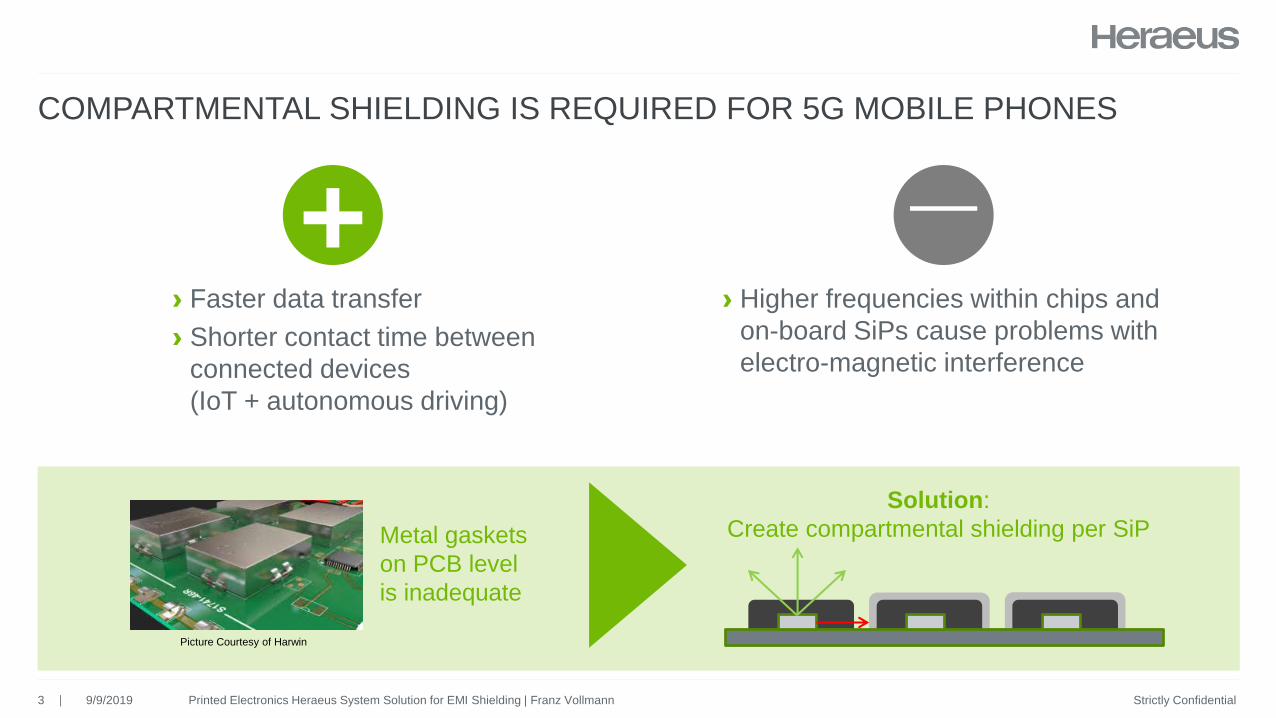
› Faster data transfer
› Shorter contact time between
connected devices
(IoT + autonomous driving)
COMPARTMENTAL SHIELDING IS REQUIRED FOR 5G MOBILE PHONES
Printed Electronics Heraeus System Solution for EMI Shielding | Franz Vollmann Strictly Confidential3
› Higher frequencies within chips and
on-board SiPs cause problems with
electro-magnetic interference
Metal gaskets
on PCB level
is inadequate
Picture Courtesy of Harwin
Solution:
Create compartmental shielding per SiP
+_
9/9/2019

COMPETING TECHNOLOGIES FOR EMI SHIELDING
Printed Electronics Heraeus System Solution for EMI Shielding | Franz Vollmann Strictly Confidential4
Existing Technology
Metal gaskets on PCB level
Picture Courtesy of Harwin
PVD Sputtering
Picture Courtesy of SigmaAldrich
Ag Nano Ink Spray
Picture Courtesy of Henkel
Ag MOD Inkjet
Next Gen Technologies
9/9/2019
Not possible for 5G SIP packages due
to formfactor requirements (space and
weight)
Expensive (hi capex, low UPH, large
footprint, clean-room requirement)
Low material efficiency
No selective coating possible
Aspect ratio of 1:0.9 not possible
Nozzle clogging due to nano particles
EHS risk due to nano particles
Low material efficiency
Sidewall coverage very challenging
No selective coating possible

HERAEUS SOLUTION FOR ELECTROMAGNETIC SHIELDING SHOWS
SUPERIOR PERFORMANCE
Printed Electronics Heraeus System Solution for EMI Shielding | Franz Vollmann Strictly Confidential9/9/20195
Factor of 5less capex,
smaller footprint
-60 dBshielding
performance
~ 1ratio between side
wall and top coating
thickness
50%lower
cost of ownership
Factor of 5higher
process speed
Zero Wasteaccurate and
targeted deposition,
selective shielding
Advantages of Heraeus solution compared to sputter
0

HERAEUS SOLUTION IS BASED ON DIGITAL PRINTING OF PARTICLE FREE
SILVER INK
Printed Electronics Heraeus System Solution for EMI Shielding | Franz Vollmann Strictly Confidential9/9/20196
MOD Ink
› Particle-free Ag ink
› No EHS concerns
› No clogging
Inkjet Printing Process
› High-speed digital printing
› Up to 15,000 UPH (10 x 10 mm SiP)
› Full set of optimized printing
parameters
Complete Curing Process
› Curing system (IR, UV, Flash)
› Optimal Ag crystal structure and
conductivity
› Full set of optimized curing
parameters
Heraeus Complete System Solution approach for product and process

TECHNOLOGY COMPARISON DEMONSTRATES SUPERIOR PERFORMANCE
OF DIGITAL PRINTING VERSUS SPUTTERING AND SPRAY
Printed Electronics Heraeus System Solution for EMI Shielding | Franz Vollmann Strictly Confidential7
Customer key requirements Sputtering (Cu coating) Spray (Nano Ag inks)Digital Printing
MOD Ag-ink (Ink-jet)
Capital Investment Very high ($2-3 mn) Low Low
Equipment Footprint Large Small Small
Material Efficiency Very low (≈35%) Low (60-70%) High (98-99%)
Total Cost of Ownership Very high Moderate Low
Throughput (UPH) Moderate High High
Production Scalability Low Moderate High
Required Coating Thickness 5-9 µm 3-6 µm 1-2 µm
Aspect Ratio (Top vs Sidewall) 1: (0.4-0.5) 1: (0.4-0.5) 1:(0.8-0.9)
Overspray/Overcoating High High Very low
Selective Coating (partial printing) ✗ masking necessary ✗ masking necessary ✓
Inkjet Marking (replace laser marking) ✗ masking possible ✗ masking possible ✓
9/9/2019

Expertise in
recipes & mass production of inks and coatings
HERAEUS IS THE PARTNER OF CHOICE FOR EMI SHIELDING: OUR IN-HOUSE
EXPERTISE IS THE BASIS FOR OUR INTEGRATED SOLUTION
Expertise in
inkjet printing systems & process know-how
Expertise in
curing lamp systems & process know-how
Printed Electronics Heraeus System Solution for EMI Shielding | Franz Vollmann Strictly Confidential8 9/9/2019

› Absolute shielding performance starts at <-40 dB
› Reaches <-60 dB for frequencies above 2.6 GHz
› Continues between -60 dB and -90 dB up to 9GHz
› No decrease of shielding performance above 10 GHz
SHIELDING EFFECTIVENESS IS ABOVE -40 DB FOR THE ENTIRE FREQUENCY
RANGE
Printed Electronics Heraeus System Solution for EMI Shielding | Franz Vollmann Strictly Confidential9
Absolute shielding
performance uncoated part
Absolute shielding
performance coated part
9/9/2019

Printed Electronics Heraeus System Solution for EMI Shielding | Franz Vollmann Strictly Confidential10
FIB results show a very homogeneous layer on the EMC
9/9/2019
DIGITAL PRINTING RESULTS IN VERY HOMOGENEOUS SILVER LAYER

HERAEUS SOLUTION ALLOWS SELECTIVE SHIELDING
Printed Electronics Heraeus System Solution for EMI Shielding | Franz Vollmann Strictly Confidential11
› Silver ink printed on
epoxy mold part
› Sharp edge between
printed and not printed
area
Example Result Detail
› 4 layers printed on top› Width of transition area:
< 100 µm
› Includes positioning
between layers
9/9/2019

Microscope Picture of Top and Side Thickness
▪ Results of tests on glass dummies (ultra-smooth surface)
▪ Achieved aspect ratio approx. 1 : 0.9
ASPECT RATIO TOP SIDE THICKNESS VS. SIDE WALL THICKNESS
MP 1MP 2
MP 3
MP 4
MP 5
MP 6
MP 2 (Top Surface) MP 6 (Side Wall)
Printed Electronics Heraeus System Solution for EMI Shielding | Franz Vollmann Strictly Confidential9/9/201912

THE DEMONSTRATOR EQUIPMENT FOR TESTS AT CUSTOMER SITE IS
AVAILABLE Q4/2019 AND THE MANUFACTURING SOLUTION Q2/2020
Printed Electronics Heraeus System Solution for EMI Shielding | Franz Vollmann Strictly Confidential9/9/201913
› Joint projects
with lead
customers
commenced
› Ramp up project
team in Asia
Development Data ValidationCustomer
Joint Project
Prototype
Line
Commercial
Availability
Q4 2019 Q2 2020
Q3 2019
today
› In-line solution
› At-line solution

OUR EMI SHIELDING SOLUTION CAN BE USED FOR A BROAD RANGE OF
APPLICATIONS
Printed Electronics Heraeus System Solution for EMI Shielding | Franz Vollmann Strictly Confidential14
› Tightly packed highly sensitive components
› Constant move toward miniaturization
› Growing wireless technology applications
› System-in-Package (SiP)
› System-on-Chip (SoC)
› Microcontrollers (MCU)
› PCB
› Power amplifiers
› Wireless modules (Wi-Fi, Bluetooth)
› Radio Frequency (RF) modules
› Memory
› Sensors
› Digital Signal Processors (DSP)
› Application-specific integrated circuits (ASIC)
› Field-programmable gate arrays (FPGA)
› Analog-Digital Converters (ADC)
Where is it required?Heraeus solution is applicable to various
components
9/9/2019

Printed Electronics Heraeus System Solution for EMI Shielding | Franz Vollmann Strictly Confidential15 9/9/2019
VISIT US @:
OR CONTACT US AT:
Visit us @ Booth #I2408
(1st Floor)
賀利氏誠邀您莅臨#I2408 展位 (一樓)