temperature and power supply system monitors datasheet
TRANSCRIPT
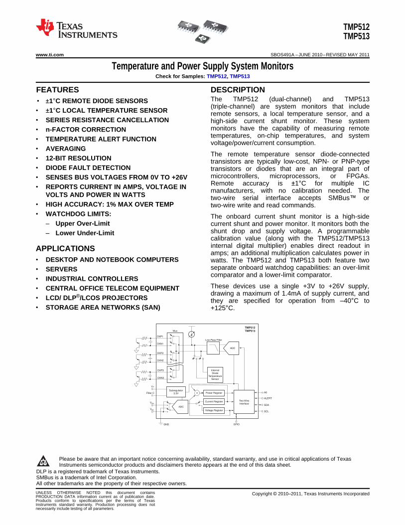
GND GPIO
VIN+
VIN-
ALERT
SDA
SCL
ADC
TMP512
TMP513
DXP1
DXN1
DXP2
DXN2
Subregulator
3.3V
V+
Filter C
Two-Wire
Interface
Power Register
Current Register
Voltage Register
ADC
Low-Pass Filter
Internal
Diode
Temperature
Sensor
Mux
A0
DXP3
DXN3
TMP512TMP513
www.ti.com SBOS491A –JUNE 2010–REVISED MAY 2011
Temperature and Power Supply System MonitorsCheck for Samples: TMP512, TMP513
1FEATURES DESCRIPTIONThe TMP512 (dual-channel) and TMP513
234• ±1°C REMOTE DIODE SENSORS(triple-channel) are system monitors that include• ±1°C LOCAL TEMPERATURE SENSOR remote sensors, a local temperature sensor, and a
• SERIES RESISTANCE CANCELLATION high-side current shunt monitor. These systemmonitors have the capability of measuring remote• n-FACTOR CORRECTIONtemperatures, on-chip temperatures, and system• TEMPERATURE ALERT FUNCTION voltage/power/current consumption.
• AVERAGINGThe remote temperature sensor diode-connected• 12-BIT RESOLUTION transistors are typically low-cost, NPN- or PNP-type
• DIODE FAULT DETECTION transistors or diodes that are an integral part ofmicrocontrollers, microprocessors, or FPGAs.• SENSES BUS VOLTAGES FROM 0V TO +26VRemote accuracy is ±1°C for multiple IC• REPORTS CURRENT IN AMPS, VOLTAGE IN manufacturers, with no calibration needed. The
VOLTS AND POWER IN WATTS two-wire serial interface accepts SMBus™ or• HIGH ACCURACY: 1% MAX OVER TEMP two-wire write and read commands.• WATCHDOG LIMITS: The onboard current shunt monitor is a high-side
– Upper Over-Limit current shunt and power monitor. It monitors both theshunt drop and supply voltage. A programmable– Lower Under-Limitcalibration value (along with the TMP512/TMP513internal digital multiplier) enables direct readout inAPPLICATIONSamps; an additional multiplication calculates power in
• DESKTOP AND NOTEBOOK COMPUTERS watts. The TMP512 and TMP513 both feature twoseparate onboard watchdog capabilities: an over-limit• SERVERScomparator and a lower-limit comparator.• INDUSTRIAL CONTROLLERSThese devices use a single +3V to +26V supply,• CENTRAL OFFICE TELECOM EQUIPMENTdrawing a maximum of 1.4mA of supply current, and
• LCD/ DLP®/LCOS PROJECTORS they are specified for operation from –40°C to• STORAGE AREA NETWORKS (SAN) +125°C.
1
Please be aware that an important notice concerning availability, standard warranty, and use in critical applications of TexasInstruments semiconductor products and disclaimers thereto appears at the end of this data sheet.
2DLP is a registered trademark of Texas Instruments.3SMBus is a trademark of Intel Corporation.4All other trademarks are the property of their respective owners.
UNLESS OTHERWISE NOTED this document contains Copyright © 2010–2011, Texas Instruments IncorporatedPRODUCTION DATA information current as of publication date.Products conform to specifications per the terms of TexasInstruments standard warranty. Production processing does notnecessarily include testing of all parameters.
TMP512TMP513
SBOS491A –JUNE 2010–REVISED MAY 2011 www.ti.com
This integrated circuit can be damaged by ESD. Texas Instruments recommends that all integrated circuits be handled withappropriate precautions. Failure to observe proper handling and installation procedures can cause damage.
ESD damage can range from subtle performance degradation to complete device failure. Precision integrated circuits may be moresusceptible to damage because very small parametric changes could cause the device not to meet its published specifications.
PACKAGE INFORMATION (1)
PRODUCT PACKAGE-LEAD PACKAGE DESIGNATOR PACKAGE MARKING
SO-14 D TMP512ATMP512
QFN-16 RSA TMP512A
SO-16 D TMP513ATMP513
QFN-16 RSA TMP513A
(1) For the most current package and ordering information see the Package Option Addendum at the end of this document, or visit theTMP512/TMP513 product folder at www.ti.com.
ABSOLUTE MAXIMUM RATINGS (1)
Over operating free-air temperature range (unless otherwise noted).
TMP512, TMP513 UNIT
Supply Voltage, V+ 26 V
Voltage GND – 0.3 to +6 VFilter C
Current 10 mA
Differential (VIN+) – (VIN–)(2) –26 to +26 V
Analog Inputs, VIN+, VIN–Common-Mode –0.3 to +26 V
Open-Drain Digital Outputs GND – 0.3 to +6 V
GPIO, DXP, DXN GND – 0.3 to V+ + 0.3 V
Input Current Into Any Pin 5 mA
Open-Drain Digital Output Current 10 mA
Storage Temperature –65 to +150 °CJunction Temperature +150 °C
Human Body Model (HBM) 2000 V
ESD Ratings Charged-Device Model (CDM) 1000 V
Machine Model (MM) 150 V
(1) Stresses above these ratings may cause permanent damage. Exposure to absolute maximum conditions for extended periods maydegrade device reliability. These are stress ratings only, and functional operation of the device at these or any other conditions beyondthose specified is not implied.
(2) VIN+ and VIN– may have a differential voltage of –26V to +26V; however, the voltage at these pins must not exceed the range –0.3V to+26V.
2 Copyright © 2010–2011, Texas Instruments Incorporated
TMP512TMP513
www.ti.com SBOS491A –JUNE 2010–REVISED MAY 2011
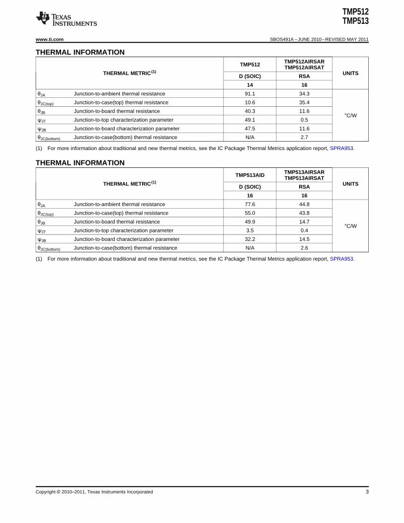
THERMAL INFORMATIONTMP512AIRSARTMP512 TMP512AIRSAT
THERMAL METRIC (1) UNITSD (SOIC) RSA
14 16
θJA Junction-to-ambient thermal resistance 91.1 34.3
θJC(top) Junction-to-case(top) thermal resistance 10.6 35.4
θJB Junction-to-board thermal resistance 40.3 11.6°C/W
ψJT Junction-to-top characterization parameter 49.1 0.5
ψJB Junction-to-board characterization parameter 47.5 11.6
θJC(bottom) Junction-to-case(bottom) thermal resistance N/A 2.7
(1) For more information about traditional and new thermal metrics, see the IC Package Thermal Metrics application report, SPRA953.
THERMAL INFORMATIONTMP513AIRSARTMP513AID TMP513AIRSAT
THERMAL METRIC (1) UNITSD (SOIC) RSA
16 16
θJA Junction-to-ambient thermal resistance 77.6 44.8
θJC(top) Junction-to-case(top) thermal resistance 55.0 43.8
θJB Junction-to-board thermal resistance 49.9 14.7°C/W
ψJT Junction-to-top characterization parameter 3.5 0.4
ψJB Junction-to-board characterization parameter 32.2 14.5
θJC(bottom) Junction-to-case(bottom) thermal resistance N/A 2.6
(1) For more information about traditional and new thermal metrics, see the IC Package Thermal Metrics application report, SPRA953.
Copyright © 2010–2011, Texas Instruments Incorporated 3
TMP512TMP513
SBOS491A –JUNE 2010–REVISED MAY 2011 www.ti.com
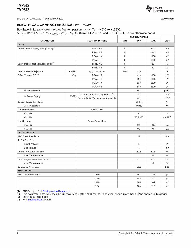
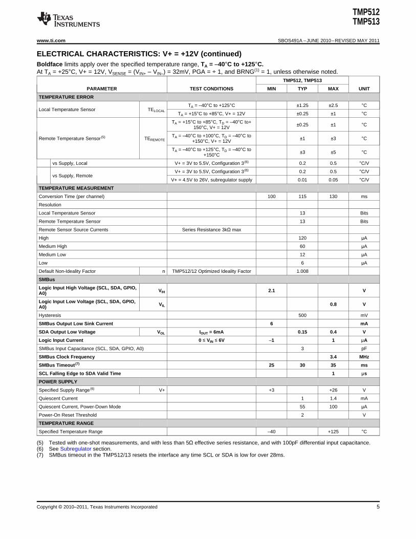
ELECTRICAL CHARACTERISTICS: V+ = +12VBoldface limits apply over the specified temperature range, TA = –40°C to +125°C.At TA = +25°C, V+ = 12V, VSENSE = (VIN+ – VIN–) = 32mV, PGA = ÷ 1, and BRNG (1) = 1, unless otherwise noted.
TMP512, TMP513
PARAMETER TEST CONDITIONS MIN TYP MAX UNIT
INPUT
Current Sense (Input) Voltage Range PGA = ÷ 1 0 ±40 mV
PGA = ÷ 2 0 ±80 mV
PGA = ÷ 4 0 ±160 mV
PGA = ÷ 8 0 ±320 mV
Bus Voltage (Input Voltage) Range (2) BRNG = 0 0 16 V
BRNG = 1 0 32 V
Common-Mode Rejection CMRR VIN+ = 0V to 26V 100 120 dB
Offset Voltage, RTI (3) VOS PGA = ÷ 1 ±10 ±100 μV
PGA = ÷ 2 ±20 ±125 μV
PGA = ÷ 4 ±30 ±150 μV
PGA = ÷ 8 ±40 ±200 μV
vs Temperature 0.2 μV/°C
V+ = 3V to 5.5V, Configuration 3 (4) 10 μV/Vvs Power Supply PSRR
V+ = 4.5V to 26V, subregulator supply 0.1 μV/V
Current Sense Gain Error ±0.04 %
vs Temperature 0.0025 %
Input Impedance Active Mode
VIN+ Pin 20 μA
VIN– Pin 20 || 320 μA || kΩ
Input Leakage Power-Down Mode
VIN+ Pin 0.1 0.5 μA
VIN– Pin 0.1 0.5 μA
DC ACCURACY
ADC Basic Resolution 12 Bits
1 LSB Step Size
Shunt Voltage 10 μV
Bus Voltage 4 mV
Current Measurement Error ±0.2 ±0.5 %
over Temperature ±1 %
Bus Voltage Measurement Error ±0.2 ±0.5 %
over Temperature ±1 %
Differential Nonlinearity ±0.1 LSB
ADC TIMING
ADC Conversion Time 12-Bit 665 733 μs
11-Bit 345 380 μs
10-Bit 185 204 μs
9-Bit 105 117 μs
(1) BRNG is bit 13 of Configuration Register 1.(2) This parameter only expresses the full-scale range of the ADC scaling. In no event should more than 26V be applied to this device.(3) Referred-to-input (RTI).(4) See Subregulator section.
4 Copyright © 2010–2011, Texas Instruments Incorporated
TMP512TMP513
www.ti.com SBOS491A –JUNE 2010–REVISED MAY 2011
ELECTRICAL CHARACTERISTICS: V+ = +12V (continued)Boldface limits apply over the specified temperature range, TA = –40°C to +125°C.At TA = +25°C, V+ = 12V, VSENSE = (VIN+ – VIN–) = 32mV, PGA = ÷ 1, and BRNG(1) = 1, unless otherwise noted.
TMP512, TMP513
PARAMETER TEST CONDITIONS MIN TYP MAX UNIT
TEMPERATURE ERROR
TA = –40°C to +125°C ±1.25 ±2.5 °CLocal Temperature Sensor TELOCAL
TA = +15°C to +85°C, V+ = 12V ±0.25 ±1 °C
TA = +15°C to +85°C, TD = –40°C to+ ±0.25 ±1 °C150°C, V+ = 12V
TA = –40°C to +100°C, TD = –40°C toRemote Temperature Sensor (5) TEREMOTE ±1 ±3 °C+150°C, V+ = 12V
TA = –40°C to +125°C, TD = –40°C to ±3 ±5 °C+150°C
vs Supply, Local V+ = 3V to 5.5V, Configuration 3 (6) 0.2 0.5 °C/V
V+ = 3V to 5.5V, Configuration 3 (6) 0.2 0.5 °C/Vvs Supply, Remote
V+ = 4.5V to 26V, subregulator supply 0.01 0.05 °C/V
TEMPERATURE MEASUREMENT
Conversion Time (per channel) 100 115 130 ms
Resolution
Local Temperature Sensor 13 Bits
Remote Temperature Sensor 13 Bits
Remote Sensor Source Currents Series Resistance 3kΩ max
High 120 μA
Medium High 60 μA
Medium Low 12 μA
Low 6 μA
Default Non-Ideality Factor n TMP512/12 Optimized Ideality Factor 1.008
SMBus
Logic Input High Voltage (SCL, SDA, GPIO, VIH 2.1 VA0)
Logic Input Low Voltage (SCL, SDA, GPIO, VIL 0.8 VA0)
Hysteresis 500 mV
SMBus Output Low Sink Current 6 mA
SDA Output Low Voltage VOL IOUT = 6mA 0.15 0.4 V
Logic Input Current 0 ≤ VIN ≤ 6V –1 1 μA
SMBus Input Capacitance (SCL, SDA, GPIO, A0) 3 pF
SMBus Clock Frequency 3.4 MHz
SMBus Timeout (7) 25 30 35 ms
SCL Falling Edge to SDA Valid Time 1 μs
POWER SUPPLY
Specified Supply Range (6) V+ +3 +26 V
Quiescent Current 1 1.4 mA
Quiescent Current, Power-Down Mode 55 100 μA
Power-On Reset Threshold 2 V
TEMPERATURE RANGE
Specified Temperature Range –40 +125 °C
(5) Tested with one-shot measurements, and with less than 5Ω effective series resistance, and with 100pF differential input capacitance.(6) See Subregulator section.(7) SMBus timeout in the TMP512/13 resets the interface any time SCL or SDA is low for over 28ms.
Copyright © 2010–2011, Texas Instruments Incorporated 5
1
2
3
4
5
6
7
VIN-
SDA
SCL
A0
VIN+
V+
Filter C
DXP2
DXN1
DXP1
GPIO
ALERT
GND
DXN2
14
13
12
11
10
9
8
TMP512 VIN+
VIN-
SDA
SCL
GPIO
DXN2
DXP2
DXN1
12
11
10
9
Filte
r C
1
2
3
4
5 6 7 813
14
15
16
A0
NC
NC
DX
P1
ALE
RT
GN
D
V+
TMP512
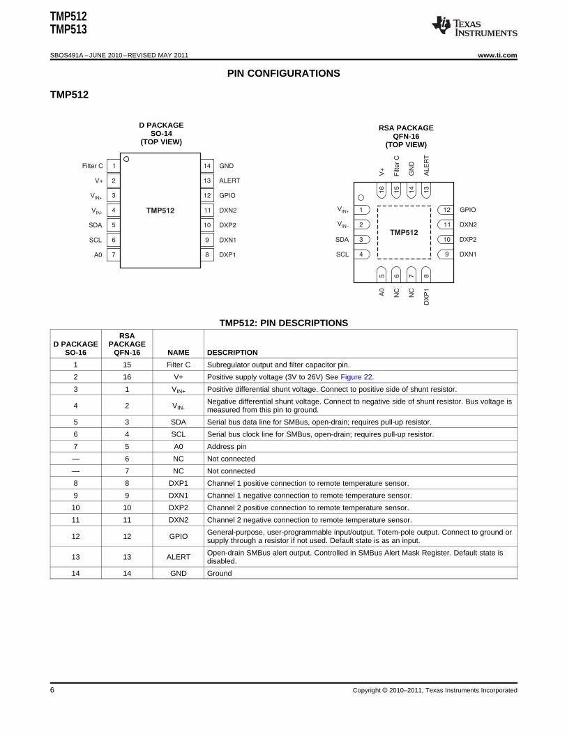
TMP512TMP513
SBOS491A –JUNE 2010–REVISED MAY 2011 www.ti.com
PIN CONFIGURATIONS
TMP512
space
D PACKAGE RSA PACKAGESO-14 QFN-16
(TOP VIEW) (TOP VIEW)
TMP512: PIN DESCRIPTIONSRSA
D PACKAGE PACKAGESO-16 QFN-16 NAME DESCRIPTION
1 15 Filter C Subregulator output and filter capacitor pin.
2 16 V+ Positive supply voltage (3V to 26V) See Figure 22.
3 1 VIN+ Positive differential shunt voltage. Connect to positive side of shunt resistor.
Negative differential shunt voltage. Connect to negative side of shunt resistor. Bus voltage is4 2 VIN- measured from this pin to ground.
5 3 SDA Serial bus data line for SMBus, open-drain; requires pull-up resistor.
6 4 SCL Serial bus clock line for SMBus, open-drain; requires pull-up resistor.
7 5 A0 Address pin
— 6 NC Not connected
— 7 NC Not connected
8 8 DXP1 Channel 1 positive connection to remote temperature sensor.
9 9 DXN1 Channel 1 negative connection to remote temperature sensor.
10 10 DXP2 Channel 2 positive connection to remote temperature sensor.
11 11 DXN2 Channel 2 negative connection to remote temperature sensor.
General-purpose, user-programmable input/output. Totem-pole output. Connect to ground or12 12 GPIO supply through a resistor if not used. Default state is as an input.
Open-drain SMBus alert output. Controlled in SMBus Alert Mask Register. Default state is13 13 ALERT disabled.
14 14 GND Ground
6 Copyright © 2010–2011, Texas Instruments Incorporated
1
2
3
4
5
6
7
8
16
15
14
13
12
11
10
9
Filter C
V+
VIN+
VIN-
SDA
SCL
A0
DXP1
GND
ALERT
GPIO
DXN3
DXP3
DXN2
DXP2
DXN1
TMP513
VIN+
VIN-
SDA
SCL
GPIO
DXN3
DXP3
DXN2
12
11
10
9
Filte
r C
1
2
3
4
5 6 7 813
14
15
16
A0
DX
P1
DX
N1
DX
P2
ALE
RT
GN
D
V+
TMP513
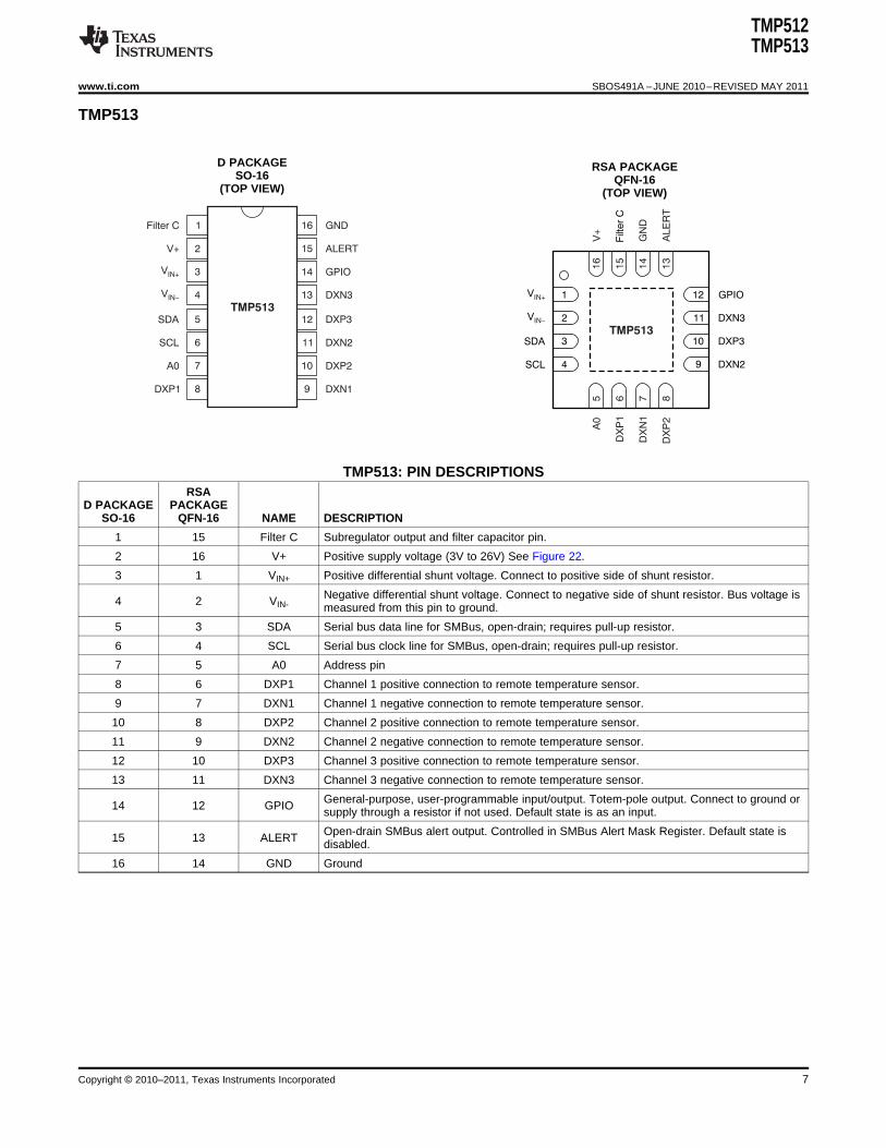
TMP512TMP513
www.ti.com SBOS491A –JUNE 2010–REVISED MAY 2011
TMP513
space
D PACKAGE RSA PACKAGESO-16 QFN-16
(TOP VIEW) (TOP VIEW)
TMP513: PIN DESCRIPTIONSRSA
D PACKAGE PACKAGESO-16 QFN-16 NAME DESCRIPTION
1 15 Filter C Subregulator output and filter capacitor pin.
2 16 V+ Positive supply voltage (3V to 26V) See Figure 22.
3 1 VIN+ Positive differential shunt voltage. Connect to positive side of shunt resistor.
Negative differential shunt voltage. Connect to negative side of shunt resistor. Bus voltage is4 2 VIN- measured from this pin to ground.
5 3 SDA Serial bus data line for SMBus, open-drain; requires pull-up resistor.
6 4 SCL Serial bus clock line for SMBus, open-drain; requires pull-up resistor.
7 5 A0 Address pin
8 6 DXP1 Channel 1 positive connection to remote temperature sensor.
9 7 DXN1 Channel 1 negative connection to remote temperature sensor.
10 8 DXP2 Channel 2 positive connection to remote temperature sensor.
11 9 DXN2 Channel 2 negative connection to remote temperature sensor.
12 10 DXP3 Channel 3 positive connection to remote temperature sensor.
13 11 DXN3 Channel 3 negative connection to remote temperature sensor.
General-purpose, user-programmable input/output. Totem-pole output. Connect to ground or14 12 GPIO supply through a resistor if not used. Default state is as an input.
Open-drain SMBus alert output. Controlled in SMBus Alert Mask Register. Default state is15 13 ALERT disabled.
16 14 GND Ground
Copyright © 2010–2011, Texas Instruments Incorporated 7
-40 -25 0 25 50 75 100 125
6
5
4
3
2
1
0
1
2
3
4
5
6
-
-
-
-
-
-
Re
mo
te T
em
pe
ratu
re E
rro
r (
C)
?
Ambient Temperature ( C)?
34 Units Shown
10 100 1k 10k 100k 1M
Ga
in (
dB
)
Input Frequency (Hz)
0
10
20
30
40
50
60
70
80
90
100
-
-
-
-
-
-
-
-
-
-
-40 -25 0 25 50 75 100
Lo
ca
l Te
mp
era
ture
Err
or
(C
)°
Ambient Temperature ( C)°
125
14 Units Shown
2.0
1.5
1.0
0.5
0
0.5
1.0
1.5
2.0
-
-
-
-
-40 -25 0 25 50 75 100
Off
se
t (
V)
m
Temperature ( C)°
125
15
10
5
0
5
10
15
-
-
-
40mV Range
80mV Range
160mV Range
320mV Range
-40 -25 0 25 50 75 100
Ga
in E
rro
r (m
%)
Temperature ( C)°
125
250
200
150
100
50
0
50
100
-
-
320mV Range
160mV Range
80mV Range
40mV Range
-40 -25 0 25 50 75 100
Off
se
t (m
V)
Temperature ( C)°
125
32V Range
16V Range
35
30
25
20
15
10
5
0
5
10
15
-
-
-
TMP512TMP513
SBOS491A –JUNE 2010–REVISED MAY 2011 www.ti.com
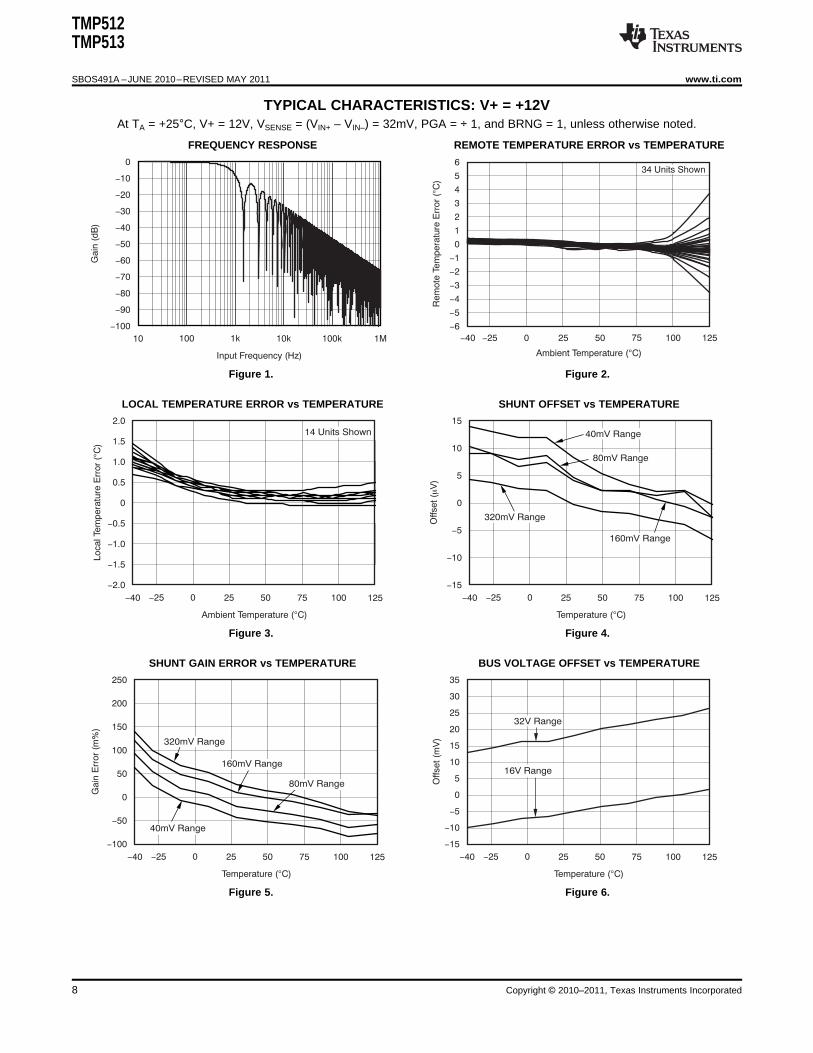
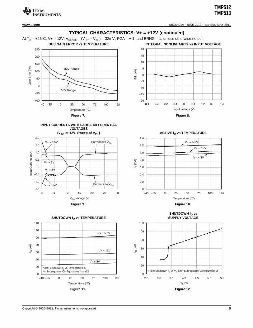
TYPICAL CHARACTERISTICS: V+ = +12VAt TA = +25°C, V+ = 12V, VSENSE = (VIN+ – VIN–) = 32mV, PGA = ÷ 1, and BRNG = 1, unless otherwise noted.
FREQUENCY RESPONSE REMOTE TEMPERATURE ERROR vs TEMPERATURE
Figure 1. Figure 2.
LOCAL TEMPERATURE ERROR vs TEMPERATURE SHUNT OFFSET vs TEMPERATURE
Figure 3. Figure 4.
SHUNT GAIN ERROR vs TEMPERATURE BUS VOLTAGE OFFSET vs TEMPERATURE
Figure 5. Figure 6.
8 Copyright © 2010–2011, Texas Instruments Incorporated
20
15
10
5
0
-5
-10
-15
-20
-0.4 -0.3 -0.2 -0.1 0 0.1 0.2 0.3
INL
(V
)m
Input Voltage (V)
0.4-40 -25 0 25 50 75 100
Ga
in E
rror
(m%
)
Temperature ( C)°
125
250
200
150
100
50
0
50
100
-
-
32V Range
16V Range
0 5 10 15 20 25
Input C
urr
ents
(m
A)
V Voltage (V)IN-
30
2.0
1.5
1.0
0.5
0
0.5
1.0
1.5
-
-
-
V+ = 5.5V
V+ 5.5V=
V+ = 3V
V+ 3V=
Current into VIN-
Current into VIN+
-40 -25 0 25 50 75 100
I(m
A)
Q
Temperature ( C)°
125
V+ = 5.5V
V+ = 12V
V+ = 3V
1.4
1.2
1.0
0.8
0.6
0.4
0.2
0
I(
)Q
mA
V (S V)
4.53.0 3.5 4.0 5.55.02.5
120
100
80
60
40
20
0Note: Shutdown I vs V is for Subregulator Configuration 3Q S
-40 -25 0 25 125
I(
A)
mQ
Temperature ( C)°
V+ = 5.5V
V+ = 12V
V+ = 3V
50 75 100
140
120
100
80
60
40
20
0
Note: Shutdown I vs Temperature is
for Subregulator Configurations 1 and 2Q
TMP512TMP513
www.ti.com SBOS491A –JUNE 2010–REVISED MAY 2011
TYPICAL CHARACTERISTICS: V+ = +12V (continued)At TA = +25°C, V+ = 12V, VSENSE = (VIN+ – VIN–) = 32mV, PGA = ÷ 1, and BRNG = 1, unless otherwise noted.
BUS GAIN ERROR vs TEMPERATURE INTEGRAL NONLINEARITY vs INPUT VOLTAGE
Figure 7. Figure 8.
INPUT CURRENTS WITH LARGE DIFFERENTIALVOLTAGES
(VIN+ at 12V, Sweep of VIN–) ACTIVE IQ vs TEMPERATURE
Figure 9. Figure 10.
SHUTDOWN IQ vsSHUTDOWN IQ vs TEMPERATURE SUPPLY VOLTAGE
Figure 11. Figure 12.
Copyright © 2010–2011, Texas Instruments Incorporated 9
1k 10k 100k 1M 10M
I(
A)
mQ
SCL Frequency (Hz)
V+ = 12V
V+ = 3.3V
1100
1050
1000
950
900
850
800
1k 10k 100k 1M 10M
I(
A)
mQ
SCL Frequency (Hz)
250
200
150
100
50
0
V+ = 12V
V+ = 3.3V
TMP512TMP513
SBOS491A –JUNE 2010–REVISED MAY 2011 www.ti.com
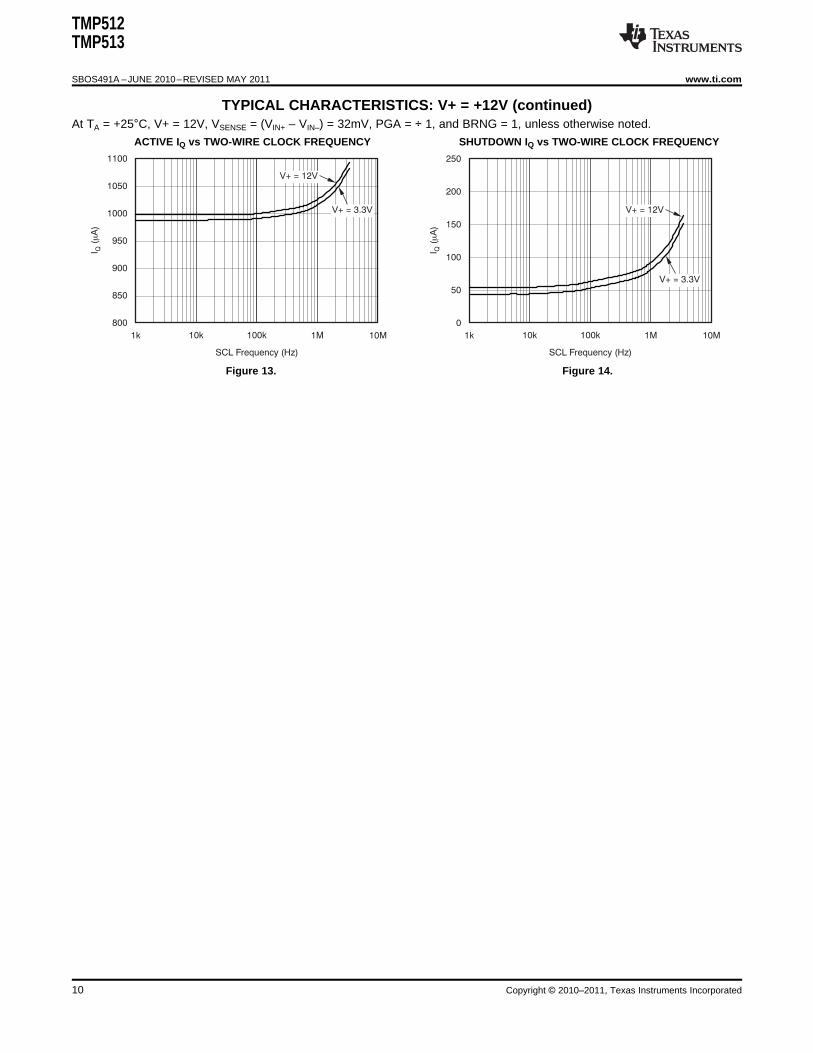
TYPICAL CHARACTERISTICS: V+ = +12V (continued)At TA = +25°C, V+ = 12V, VSENSE = (VIN+ – VIN–) = 32mV, PGA = ÷ 1, and BRNG = 1, unless otherwise noted.
ACTIVE IQ vs TWO-WIRE CLOCK FREQUENCY SHUTDOWN IQ vs TWO-WIRE CLOCK FREQUENCY
Figure 13. Figure 14.
10 Copyright © 2010–2011, Texas Instruments Incorporated

Re
mo
te T
em
pe
ratu
re E
rro
r (
)°C
R (W)S
2.0
1.5
1.0
0.5
0
-0.5
-1.0
-1.5
-2.0
0 3500500 1000 1500 2000 2500 3000
Note: For all three subregulator configurations.
Re
mo
te T
em
pe
ratu
re E
rro
r (
)°C
R (W)S
2.0
1.5
1.0
0.5
0
-0.5
-1.0
-1.5
-2.0
0 3500500 1000 1500 2000 2500 3000
Note: For all three subregulator configurations.
3
2
1
0
-1
-2
-3
Capacitance (nF)
0 0.5 1.0 1.5 2.0 2.5 3.0
Rem
ote
Tem
pera
ture
Err
or
(C
)°
TMP512TMP513
www.ti.com SBOS491A –JUNE 2010–REVISED MAY 2011
TYPICAL CHARACTERISTICS: V+ = +12V (continued)At TA = +25°C, V+ = 12V, VSENSE = (VIN+ – VIN–) = 32mV, PGA = ÷ 1, and BRNG = 1, unless otherwise noted.
REMOTE TEMPERATURE ERROR vs SERIES REMOTE TEMPERATURE ERROR vs SERIESRESISTANCE RESISTANCE
(Diode-Connected Transistor, 2N3906 PNP) (GND Collector-Connected Transistor, 2N3906 PNP)
Figure 15. Figure 16.
REMOTE TEMPERATURE ERRORvs DIFFERENTIAL CAPACITANCE
Figure 17.
Copyright © 2010–2011, Texas Instruments Incorporated 11
(b) Diode-Connected Transistor
(a) GND Collector-Connected Transistor
DXP
DXN
RS1
(1)
RS2
(1)
DXP
DXN
RS1
(1)
RS2
(1)
(b) Diode-Connected Transistor
(a) GND Collector-Connected Transistor
DXP
DXN
CDIFF
(1)
DXP
DXN
CDIFF
(1)
TMP512TMP513
SBOS491A –JUNE 2010–REVISED MAY 2011 www.ti.com
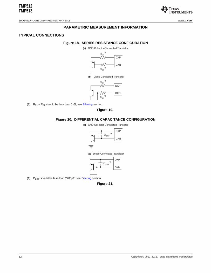
PARAMETRIC MEASUREMENT INFORMATION
TYPICAL CONNECTIONS
Figure 18. SERIES RESISTANCE CONFIGURATION
(1) RS1 + RS2 should be less than 1kΩ; see Filtering section.
Figure 19.
Figure 20. DIFFERENTIAL CAPACITANCE CONFIGURATION
(1) CDIFF should be less than 2200pF; see Filtering section.
Figure 21.
12 Copyright © 2010–2011, Texas Instruments Incorporated
Configuration 1 Configuration 2 Configuration 3
GND
ADC
Subregulator
3.3V
Subregulator
3.3V
V+ = 4.5V to 26V
Filter C
Load
470nF
Bus Voltage Range = 4.5V to 26V
Shunt
RSHUNT
VIN+
VIN-
GND
ADC
V+ = 4.5V to 26V
Load
Filter C
470nF
Bus Voltage Range = 0V to 26V
Shunt
RSHUNT
VIN+
VIN-
GND
ADC
Subregulator
3.3V
V+ = 3V to 5.5V
Load
Filter C
100nF
Bus Voltage Range = 0V to 26V
Shunt
RSHUNT
VIN+
VIN-
TMP512TMP513
www.ti.com SBOS491A –JUNE 2010–REVISED MAY 2011
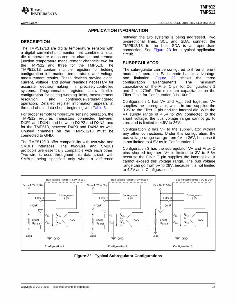
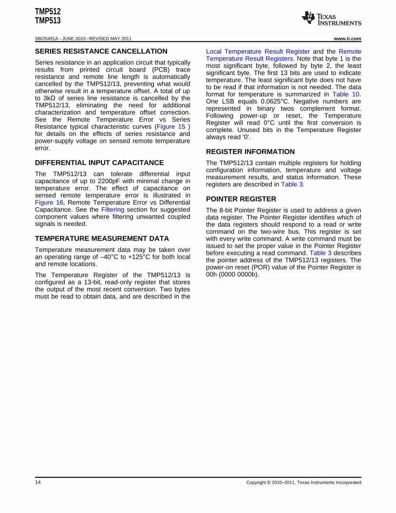
APPLICATION INFORMATION
between the two systems is being addressed. Twobi-directional lines, SCL and SDA, connect theDESCRIPTIONTMP512/13 to the bus. SDA is an open-drain
The TMP512/13 are digital temperature sensors with connection. See Figure 23 for a typical applicationa digital current-shunt monitor that combine a local circuit.die temperature measurement channel and remotejunction temperature measurement channels: two for SUBREGULATORthe TMP512 and three for the TMP513. TheTMP512/13 contain multiple registers for holding The subregulator can be configured to three differentconfiguration information, temperature, and voltage modes of operation. Each mode has its advantagemeasurement results. These devices provide digital and limitation. Figure 22 shows the threecurrent, voltage, and power readings necessary for configuration arrangements. The minimumaccurate decision-making in precisely-controlled capacitance on the Filter C pin for Configurations 1systems. Programmable registers allow flexible and 2 is 470nF. The minimum capacitance on theconfiguration for setting warning limits, measurement Filter C pin for Configuration 3 is 100nF.resolution, and continuous-versus-triggered
Configuration 1 has V+ and VIN+ tied together. V+operation. Detailed register information appears atsupplies the subregulator, which in turn supplies thethe end of this data sheet, beginning with Table 3.3.3V to the Filter C pin and the internal die. With the
For proper remote temperature sensing operation, the V+ supply range of 4.5V to 26V connected to theTMP512 requires transistors connected between shunt voltage, the bus voltage range cannot go toDXP1 and DXN1 and between DXP2 and DXN2, and zero and is limited to 4.5V to 26V.for the TMP513, between DXP3 and DXN3 as well.
Configuration 2 has V+ to the subregulator withoutUnused channels on the TMP512/13 must beany other connections. Under this configuration, theconnected to GND.bus voltage range can go from 0V to 26V, because it
The TMP512/13 offer compatibility with two-wire and is not limited to 4.5V as in Configuration 1.SMBus interfaces. The two-wire and SMBus
Configuration 3 has the subregulator V+ and Filter Cprotocols are essentially compatible with each other.pins shorted together. V+ is limited to 3V to 5.5VTwo-wire is used throughout this data sheet, withbecause the Filter C pin supplies the internal die; itSMBus being specified only when a differencecannot exceed this voltage range. The bus voltagerange can go from 0V to 26V, because it is not limitedto 4.5V as in Configuration 1.
Figure 22. Typical Subregulator Configurations
Copyright © 2010–2011, Texas Instruments Incorporated 13
TMP512TMP513
SBOS491A –JUNE 2010–REVISED MAY 2011 www.ti.com
SERIES RESISTANCE CANCELLATION Local Temperature Result Register and the RemoteTemperature Result Registers. Note that byte 1 is the
Series resistance in an application circuit that typically most significant byte, followed by byte 2, the leastresults from printed circuit board (PCB) trace significant byte. The first 13 bits are used to indicateresistance and remote line length is automatically temperature. The least significant byte does not havecancelled by the TMP512/13, preventing what would to be read if that information is not needed. The dataotherwise result in a temperature offset. A total of up format for temperature is summarized in Table 10.to 3kΩ of series line resistance is cancelled by the One LSB equals 0.0625°C. Negative numbers areTMP512/13, eliminating the need for additional represented in binary twos complement format.characterization and temperature offset correction. Following power-up or reset, the TemperatureSee the Remote Temperature Error vs Series Register will read 0°C until the first conversion isResistance typical characteristic curves (Figure 15 ) complete. Unused bits in the Temperature Registerfor details on the effects of series resistance and always read '0'.power-supply voltage on sensed remote temperatureerror. REGISTER INFORMATION
DIFFERENTIAL INPUT CAPACITANCE The TMP512/13 contain multiple registers for holdingconfiguration information, temperature and voltage
The TMP512/13 can tolerate differential input measurement results, and status information. Thesecapacitance of up to 2200pF with minimal change in registers are described in Table 3.temperature error. The effect of capacitance onsensed remote temperature error is illustrated in POINTER REGISTERFigure 16, Remote Temperature Error vs DifferentialCapacitance. See the Filtering section for suggested The 8-bit Pointer Register is used to address a givencomponent values where filtering unwanted coupled data register. The Pointer Register identifies which ofsignals is needed. the data registers should respond to a read or write
command on the two-wire bus. This register is setTEMPERATURE MEASUREMENT DATA with every write command. A write command must be
issued to set the proper value in the Pointer RegisterTemperature measurement data may be taken over before executing a read command. Table 3 describesan operating range of –40°C to +125°C for both local the pointer address of the TMP512/13 registers. Theand remote locations. power-on reset (POR) value of the Pointer Register is
00h (0000 0000b).The Temperature Register of the TMP512/13 isconfigured as a 13-bit, read-only register that storesthe output of the most recent conversion. Two bytesmust be read to obtain data, and are described in the
14 Copyright © 2010–2011, Texas Instruments Incorporated
V V =-BE2 BE1
nkT
q
I
I2
1(
(
In
n =eff
1.008 300
(300 N )- ADJUST
´
N 300ADJUST -=300 1.008
neff
´(
(
´ Power Register
Current RegisterTwo-Wire
Interface
Voltage Register
ADC
GND GPIO
DXP1
DXN1
DXP2
DXN2
ADC
Low-Pass Filter
MUX
DXP3
DXN3
VIN+
VIN-
Current
Shunt
Load
Filter C
V+Subregulator
3.3V
Internal
Diode
Temperature
Sensor
A0
ALERT
SDA
SCL
SMBus
Controller
3.3V Supply
TMP512
TMP513
TMP512TMP513
www.ti.com SBOS491A –JUNE 2010–REVISED MAY 2011
n-FACTOR CORRECTION REGISTER twos-complement format, yielding an effective datarange from –128 to +127. The n-factor value may be
The TMP512/13 allow for a different n-factor value to written to and read from pointer address 16h forbe used for converting remote channel remote channel 1, pointer address 17h for remotemeasurements to temperature. The remote channel channel 2, and pointer address 18h for remoteuses sequential current excitation to extract a channel 3. The register power-on reset value is 00h,differential VBE voltage measurement to determine thus having no effect unless the register is written to.the temperature of the remote transistor. Equation 1describes this voltage and temperature. BUS OVERVIEW
The device that initiates the transfer is called a(1) master, and the devices controlled by the master are
slaves. The bus must be controlled by a masterThe value n in Equation 1 is a characteristic of thedevice that generates the serial clock (SCL), controlsparticular transistor used for the remote channel. Thethe bus access, and generates START and STOPpower-on reset value for the TMP512/13 is n = 1.008.conditions.The value in the n-Factor Correction Register may be
used to adjust the effective n-factor according to To address a specific device, the master initiates aEquation 2 and Equation 3. START condition by pulling the data signal line (SDA)
from a HIGH to a LOW logic level while SCL is HIGH.All slaves on the bus shift in the slave address byte(2)on the rising edge of SCL, with the last bit indicatingwhether a read or write operation is intended. Duringthe ninth clock pulse, the slave being addressed(3)responds to the master by generating an
The n-factor value must be stored in Acknowledge and pulling SDA LOW.
Figure 23. Typical Application Circuit
Copyright © 2010–2011, Texas Instruments Incorporated 15
TMP512TMP513
SBOS491A –JUNE 2010–REVISED MAY 2011 www.ti.com
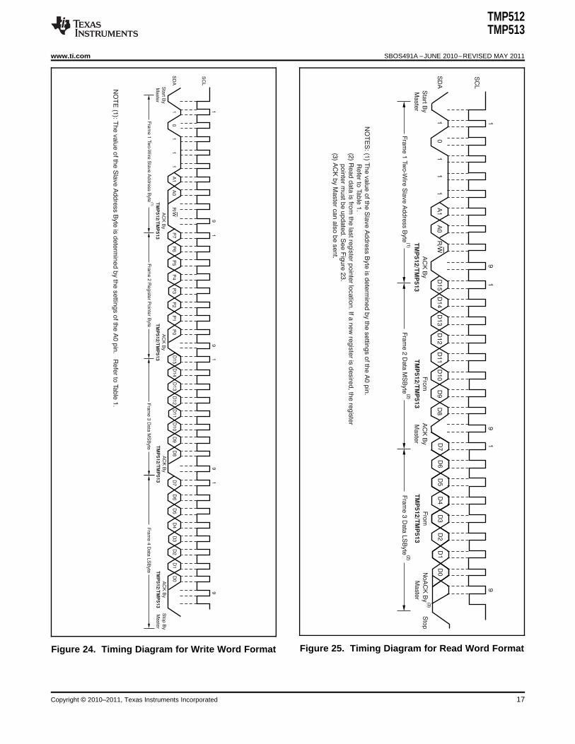
Data transfer is then initiated and eight bits of data WRITING TO/READING FROM THEare sent, followed by an Acknowledge bit. During TMP512/13data transfer, SDA must remain stable while SCL is
Accessing a particular register on the TMP512/13 isHIGH. Any change in SDA while SCL is HIGH isaccomplished by writing the appropriate value to theinterpreted as a START or STOP condition.register pointer. Refer to Table 3 for a complete list of
Once all data have been transferred, the master registers and corresponding addresses. The value forgenerates a STOP condition, indicated by pulling the register pointer as shown in Figure 26 is the firstSDA from LOW to HIGH while SCL is HIGH. The byte transferred after the slave address byte with theTMP512/13 includes a 28ms timeout on its interface R/W bit LOW. Every write operation to theto prevent locking up an SMBus. TMP512/13 requires a value for the register pointer.
Writing to a register begins with the first byteSERIAL BUS ADDRESS transmitted by the master. This byte is the slaveaddress, with the R/W bit LOW. The TMP512/13 thenTo communicate with the TMP512/13, the masteracknowledge receipt of a valid address. The nextmust first address slave devices via a slave addressbyte transmitted by the master is the address of thebyte. The slave address byte consists of sevenregister to which data will be written. This registeraddress bits, and a direction bit indicating the intentaddress value updates the register pointer to theof executing a read or write operation.desired register. The next two bytes are written to the
The TMP512/13 feature an address pin to allow up to register addressed by the register pointer. Thefour devices to be addressed on a single bus. Table 1 TMP512/13 acknowledge receipt of each data byte.describes the pin logic levels used to properly The master may terminate data transfer byconnect up to four devices. The state of the A0 pin is generating a START or STOP condition.sampled on every bus communication and should be
When reading from the TMP512/13, the last valueset before any activity on the interface occurs. Thestored in the register pointer by a write operationaddress pin is read at the start of eachdetermines which register is read during a readcommunication event.operation. To change the register pointer for a readoperation, a new value must be written to the registerTable 1. TMP512/13 Address Pins and
Slave Addresses pointer. This write is accomplished by issuing a slaveaddress byte with the R/W bit LOW, followed by theDEVICE TWO-WIREregister pointer byte. No additional data are required.ADDRESS A0 PIN CONNECTIONThe master then generates a START condition and
1011100 Groundsends the slave address byte with the R/W bit HIGH
1011101 V+ to initiate the read command. The next byte is1011110 SDA transmitted by the slave and is the most significant
byte of the register indicated by the register pointer.1011111 SCLThis byte is followed by an Acknowledge from themaster; then the slave transmits the least significantSERIAL INTERFACEbyte. The master acknowledges receipt of the data
The TMP512/13 operate only as slave devices on the byte. The master may terminate data transfer bytwo-wire bus and SMBus. SCL is an input only, and generating a Not-Acknowledge after receiving anyTMP512/13 cannot drive it. Connections to the bus data byte, or generating a START or STOP condition.are made via the open-drain I/O lines SDA and SCL. If repeated reads from the same register are desired,The SDA and SCL pins feature integrated spike it is not necessary to continually send the registersuppression filters and Schmitt triggers to minimize pointer bytes; the TMP512/13 retain the registerthe effects of input spikes and bus noise. The pointer value until it is changed by the next writeTMP512/13 support the transmission protocol for fast operation.(1kHz to 400kHz) and high-speed (1kHz to 3.4MHz)
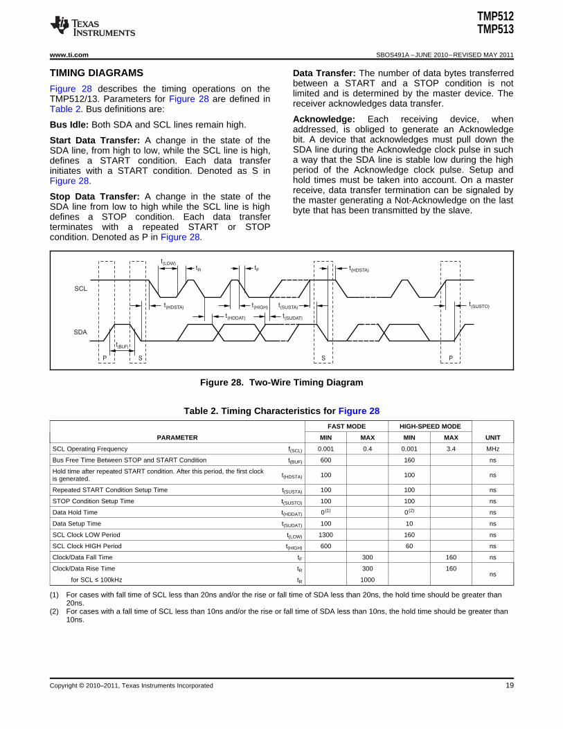
Figure 24 and Figure 25 show read and writemodes. All data bytes are transmitted MSB first.operation timing diagrams, respectively. Note thatregister bytes are sent most-significant byte first,followed by the least significant byte. See Figure 27for an illustration of a typical register pointerconfiguration.
16 Copyright © 2010–2011, Texas Instruments Incorporated
Fra
me
1 Tw
o-W
ire S
lave
Ad
dre
ss B
yte
(1)
Fra
me
2 D
ata
MS
Byte
(2)
1
Sta
rt By
Ma
ste
r
AC
K B
y
TM
P5
12
/TM
P5
13
AC
K B
y
Ma
ste
r
Fro
m
TM
P5
12
/TM
P5
13
19
19
SD
A
SC
L
01
1R
/WD
15
D1
4D
13
D1
2D
11
D1
0D
9D
81
A1
A0
Fra
me
3 D
ata
LS
Byte
(2)
Sto
pN
oA
CK
By
(3)
Ma
ste
r
Fro
m
TM
P5
12
/TM
P5
13
19
D7
D6
D5
D4
D3
D2
D1
D0
NO
TE
S: (1
) The v
alu
e o
f the S
lave A
ddre
ss B
yte
is d
ete
rmin
ed b
y th
e s
ettin
gs o
f the A
0 p
in.
Refe
r to Ta
ble
1.
(2) R
ead d
ata
is fro
m th
e la
st re
gis
ter p
oin
ter lo
catio
n. If a
new
regis
ter is
desire
d, th
e re
gis
ter
poin
ter m
ust b
e u
pdate
d. S
ee F
igure
23.
(3) A
CK
by M
aste
r can a
lso b
e s
ent.
Fra
me
1 Tw
o-W
ire S
lave
Ad
dre
ss B
yte
(1)
Fra
me
2 R
eg
iste
r Po
inte
r Byte
Sta
rt By
Ma
ste
r
AC
K B
y
TM
P5
12
/TM
P5
13
AC
K B
y
TM
P5
12
/TM
P5
13
19
1
AC
K B
y
TM
P5
12
/TM
P5
13
1
D15
D14
D13
D12
D11
D10
D9
D8
99
SD
A
SC
L
10
11
1A
1A
0R
/WP
7P
6P
5P
4P
3P
2P
1P
0
NO
TE
(1): T
he v
alu
e o
f the S
lave A
ddre
ss B
yte
is d
ete
rmin
ed b
y th
e s
ettin
gs o
f the A
0 p
in. R
efe
r to Ta
ble
1.
Fra
me
4 D
ata
LS
Byte
Fra
me
3 D
ata
MS
Byte
AC
K B
y
TM
P5
12
/TM
P5
13
Sto
p B
y
Ma
ste
r
1D7
D6
D5
D4
D3
D2
D1
D0
9
TMP512TMP513
www.ti.com SBOS491A –JUNE 2010–REVISED MAY 2011
Figure 25. Timing Diagram for Read Word FormatFigure 24. Timing Diagram for Write Word Format
Copyright © 2010–2011, Texas Instruments Incorporated 17
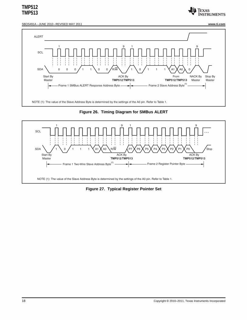
Frame 1 SMBus ALERT Response Address Byte Frame 2 Slave Address Byte(1)
Start By
Master
ACK By
TMP512/TMP513
From
TMP512/TMP513
NACK By
Master
Stop By
Master
1 9 1 9
SDA
SCL
ALERT
0 0 0 1 1 0 0 R/W 1 0 1 1 1 A1 A0 0
NOTE (1): The value of the Slave Address Byte is determined by the settings of the A0 pin. Refer to Table 1.
Frame 1 Two-Wire Slave Address Byte(1)
Frame 2 Register Pointer Byte
1
Start By
Master
ACK By
TMP512/TMP513
ACK By
TMP512/TMP513
1 9 1 9
SDA
SCL
0 1 1 1 A1 A0 R/W P7 P6 P5 P4 P3 P2 P1 P0 Stop
¼
NOTE (1): The value of the Slave Address Byte is determined by the settings of the A0 pin. Refer to Table 1.
TMP512TMP513
SBOS491A –JUNE 2010–REVISED MAY 2011 www.ti.com
Figure 26. Timing Diagram for SMBus ALERT
Figure 27. Typical Register Pointer Set
18 Copyright © 2010–2011, Texas Instruments Incorporated
SCL
SDA
t(LOW)tR tF t(HDSTA)
t(HDSTA)
t(HDDAT)
t(BUF)
t(SUDAT)
t(HIGH) t(SUSTA)t(SUSTO)
P S S P
TMP512TMP513
www.ti.com SBOS491A –JUNE 2010–REVISED MAY 2011
TIMING DIAGRAMS Data Transfer: The number of data bytes transferredbetween a START and a STOP condition is not
Figure 28 describes the timing operations on the limited and is determined by the master device. TheTMP512/13. Parameters for Figure 28 are defined in receiver acknowledges data transfer.Table 2. Bus definitions are:
Acknowledge: Each receiving device, whenBus Idle: Both SDA and SCL lines remain high. addressed, is obliged to generate an Acknowledge
bit. A device that acknowledges must pull down theStart Data Transfer: A change in the state of theSDA line during the Acknowledge clock pulse in suchSDA line, from high to low, while the SCL line is high,a way that the SDA line is stable low during the highdefines a START condition. Each data transferperiod of the Acknowledge clock pulse. Setup andinitiates with a START condition. Denoted as S inhold times must be taken into account. On a masterFigure 28.receive, data transfer termination can be signaled by
Stop Data Transfer: A change in the state of the the master generating a Not-Acknowledge on the lastSDA line from low to high while the SCL line is high byte that has been transmitted by the slave.defines a STOP condition. Each data transferterminates with a repeated START or STOPcondition. Denoted as P in Figure 28.
Figure 28. Two-Wire Timing Diagram
Table 2. Timing Characteristics for Figure 28
FAST MODE HIGH-SPEED MODE
PARAMETER MIN MAX MIN MAX UNIT
SCL Operating Frequency f(SCL) 0.001 0.4 0.001 3.4 MHz
Bus Free Time Between STOP and START Condition t(BUF) 600 160 ns
Hold time after repeated START condition. After this period, the first clock t(HDSTA) 100 100 nsis generated.
Repeated START Condition Setup Time t(SUSTA) 100 100 ns
STOP Condition Setup Time t(SUSTO) 100 100 ns
Data Hold Time t(HDDAT) 0 (1) 0 (2) ns
Data Setup Time t(SUDAT) 100 10 ns
SCL Clock LOW Period t(LOW) 1300 160 ns
SCL Clock HIGH Period t(HIGH) 600 60 ns
Clock/Data Fall Time tF 300 160 ns
Clock/Data Rise Time tR 300 160ns
for SCL ≤ 100kHz tR 1000
(1) For cases with fall time of SCL less than 20ns and/or the rise or fall time of SDA less than 20ns, the hold time should be greater than20ns.
(2) For cases with a fall time of SCL less than 10ns and/or the rise or fall time of SDA less than 10ns, the hold time should be greater than10ns.
Copyright © 2010–2011, Texas Instruments Incorporated 19
TMP512TMP513
SBOS491A –JUNE 2010–REVISED MAY 2011 www.ti.com
HIGH-SPEED MODE SENSOR FAULT
In order for the two-wire bus to operate at frequencies The TMP512/13 can sense an open circuit.above 400kHz, the master device must issue a Short-circuit conditions return a value of –256°C. TheHigh-Speed mode (Hs-mode) master code (0000 detection circuitry consists of a voltage comparator1xxx) as the first byte after a START condition to that trips when the voltage at DXP exceeds (V+) –switch the bus to high-speed operation. The 0.6V (typical). The comparator output is continuouslyTMP512/13 do not acknowledge this byte, but switch checked during a conversion. If a fault is detected,the input filters on SDA and SCL and the output filter the OPEN bit (bit 0) in the temperature result registeron SDA to operate in Hs-mode, allowing transfers at is set to '1' and the rest of the register bits should beup to 3.4MHz. After the Hs-mode master code has ignored.been issued, the master transmits a START condition
When not using the remote sensor with theto a two-wire slave address that initiates a dataTMP512/13, the DXP and DXN inputs must betransfer operation. The bus continues to operate inconnected together to prevent meaningless faultHs-mode until a STOP condition occurs on the bus.warnings.Upon receiving the STOP condition, the TMP512/13
switch the input and output filters back to Fast modeUNDERVOLTAGE LOCKOUToperation.The TMP512/13 sense when the power-supply
POWER-UP CONDITIONS voltage has reached a minimum voltage level for theADC to function. The detection circuitry consists of aPower-up conditions apply to a software reset via thevoltage comparator that enables the ADC after theRST bit (bit 15) in the Configuration Register, or thepower supply (V+) exceeds 2.7V (typical). Thetwo-wire bus General Call Reset. At device power up,comparator output is continuously checked during aall Status bits are masked, and the SMBus Alertconversion. The TMP512/13 do not perform afunction is disabled. All watchdog outputs default totemperature conversion if the power supply is notactive low and transparent (non-latched) modes.valid. The PVLD bit (see Status Register; LocalTemperature Reset Register; Remote TemperatureSHUTDOWN MODE Reset 1, 2 and 3 Registers) of the individualLocal/Remote Temperature Result Registers are setThe TMP512/13 shutdown mode of operation allowsto '1' and the temperature result may be incorrect.the user flexibility to shut down the shunt/bus voltage
measurement and the temperature measurementfunctions individually. TEMPERATURE AVERAGING
To shut down the shunt/bus voltage measurement The TMP512/13 average the input diode voltagesfunction immediately, set bits 2 through 0 in that determine the remote temperature by samplingConfiguration Register 1 (00h) to '000' respectively. multiple times throughout a conversion. TheTo shut down the shunt/bus voltage measurement temperature result can be extracted from fourafter the end of the current conversion, set bits 2 different VBE readings and is sampled 600 times inthrough 0 in Configuration Resister 1 (00h) to '100' 130ms (max). Each VBE voltage is sampled 150 timesrespectively. through integration capacitors that average the
results throughout the conversion time. A delta-sigmaTo shut down the temperature measurement function (ΔΣ) modulator and digital filter integrate the VBEimmediately, set bits 15 through 11 in Configuration voltages and create a sync filter averaging system. InRegister 2 (01h) to '00000' respectively. To shut addition, a low-pass filter is present at the input of thedown the temperature measurement after the end of converter with a cutoff frequency of 65kHz. Thisthe current conversion, set bit 15 in Configuration integrating topology offers superior noise immunity.Register 2 (01h) to '0'.
FILTERINGONE-SHOT COMMANDRemote junction temperature sensors are usually
For the TMP512/13, when the temperature core is in implemented in a noisy environment. Noise isshutdown and the voltage core is in triggered mode, a frequently generated by fast digital signals and if notsingle conversion is started on all enabled channels filtered properly will induce errors that can corruptby writing a '1' to the OS bit in Configuration Register temperature measurements. The TMP512/13 have a1. This write operation starts one conversion; the built-in 65kHz filter on the inputs of DXP and DXN toTMP512/13 returns to shutdown mode when that minimize the effects of noise. However, a bypassconversion completes. At the end of the conversion, capacitor placed differentially across the inputs of thethe Conversion Ready flags (bit 6 and bit 5) in the remote temperature sensor is recommended to makeStatus Register are set to indicate end of conversion. the application more robust against unwanted
coupled signals. The value of this capacitor should be
20 Copyright © 2010–2011, Texas Instruments Incorporated
TERR =1.004 1.008
1.008
-(
(
´ °273.15 + 100 C)
)
T = 1.48 CERR °
TERR =n 1.008
1.008
-(
(
´ °273.15 + T( C)
TMP512TMP513
www.ti.com SBOS491A –JUNE 2010–REVISED MAY 2011
between 100pF and 1nF. Some applications attain Where:better overall accuracy with additional series n = ideality factor of remote temperature sensor.resistance; however, this increased accuracy is T(°C) = actual temperature.application-specific. When series resistance is added,
TERR = error in TMP512/13 because n ≠ 1.008.the total value should not be greater than 3kΩ. IfDegree delta is the same for °C and K.filtering is needed, suggested component values are
100pF and 50Ω on each input; exact values are For n = 1.004 and T(°C) = 100°C:application-specific.
GENERAL CALL RESET
The TMP512/13 support reset via the two-wireGeneral Call address 00h (0000 0000b). The (5)TMP512/13 acknowledge the General Call address
If a discrete transistor is used as the remoteand respond to the second byte. If the second byte istemperature sensor with the TMP512/13, the best06h (0000 0110b), the TMP512/13 execute aaccuracy can be achieved by selecting the transistorsoftware reset state to all TMP512/13 registers, andaccording to the following criteria:abort any conversion in progress. The TMP512/131. Base-emitter voltage > 0.25V at 6μA, at thetake no action in response to other values in the
highest sensed temperature.second byte.2. Base-emitter voltage < 0.95V at 120μA, at the
REMOTE SENSING lowest sensed temperature.3. Base resistance < 100Ω.The TMP512/13 are designed to be used with either
discrete transistors or substrate transistors built into 4. Tight control of VBE characteristics indicated byprocessor chips and ASICs. Either NPN or PNP small variations in hFE (that is, 50 to 150).transistors can be used, as long as the base-emitter
Based on these criteria, two recommendedjunction is used as the remote temperature sense.small-signal transistors are the 2N3904 (NPN) orNPN transistors must be diode-connected. PNP2N3906 (PNP).transistors can either be transistor- or
diode-connected, as Figure 19 and Figure 21 show.BASIC ADC FUNCTIONS
Errors in remote temperature sensor readings areThe two analog inputs to the TMP512/13, VIN+ andtypically the consequence of the ideality factor andVIN–, connect to a shunt resistor in the bus of interest.current excitation used by the TMP512/13 versus theThe TMP512/13 are powered by an internalmanufacturer-specified operating current for a givensubregulator, which has a typical output of 3.3V. Thetransistor. Some manufacturers specify a high-levelbus being sensed can vary from 0V to 26V. There areand low-level current for the temperature-sensingno special considerations for power-supplysubstrate transistors. The TMP512/13 use 6μA forsequencing (for example, a bus voltage can beILOW and 120μA for IHIGH.present with the supply voltage off, and vice-versa).
The ideality factor (n) is a measured characteristic of The TMP512/13 sense the small drop across thea remote temperature sensor diode as compared to shunt for shunt voltage, and sense the voltage withan ideal diode. The TMP512/13 allow for different respect to ground from VIN– for the bus voltage. Seen-factor values; see the n-Factor Correction Register Figure 29 for an illustration of this operation.section.
When the TMP512/13 are in the normal operatingThe ideality factor for the TMP512/13 is trimmed to mode (that is, MODE bits of Configuration Register 1be 1.008. For transistors that have an ideality factor are set to '111'), the devices continuously convert thethat does not match the TMP512/13, Equation 4 can shunt voltage up to the number set in the shuntbe used to calculate the temperature error. Note that voltage averaging function (Configuration Register 1,for the equation to be used correctly, actual SADC bits). The devices then convert the bus voltagetemperature (°C) must be converted to kelvins (K). up to the number set in the bus voltage averaging
(Configuration Register 1, BADC bits). The Modecontrol in Configuration Register 1 also permits
(4) selecting modes to convert only voltage or current,either continuously or in response to a two-wirespace command.
Copyright © 2010–2011, Texas Instruments Incorporated 21
´ Power Register
Current RegisterTwo-Wire
Interface
Voltage Register
ADC
GPIO
GND
DXP1
DXN1
DXP2
DXN2
ADC
Low-Pass Filter
MUX
DXP3
DXN3
VIN+
VIN-
Current
Shunt
Load
Filter C
V+Subregulator
3.3V
Internal
Diode
Temperature
Sensor
A0
ALERT
SDA
SCL
SMBus
Controller
3.3V Supply
TMP512
TMP513
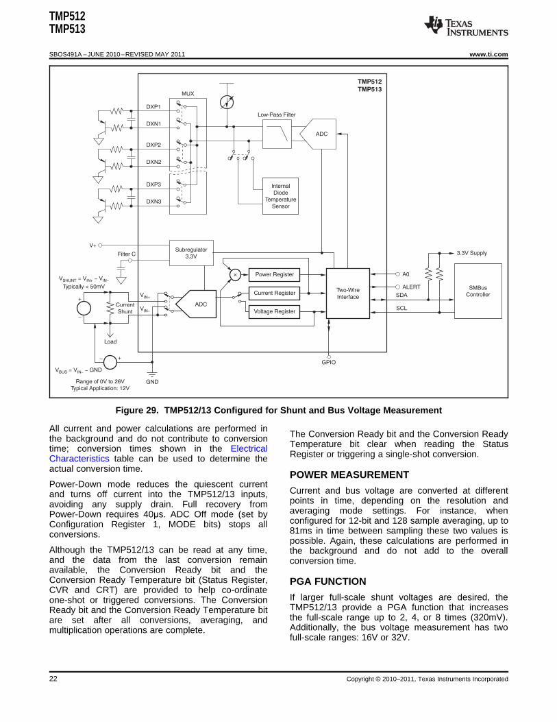
V = V -SHUNT IN+ VIN-
Typically < 50mV
V =BUS GND-VIN-
Range of 0V to 26V
Typical Application: 12V
TMP512TMP513
SBOS491A –JUNE 2010–REVISED MAY 2011 www.ti.com
Figure 29. TMP512/13 Configured for Shunt and Bus Voltage Measurement
All current and power calculations are performed inThe Conversion Ready bit and the Conversion Readythe background and do not contribute to conversionTemperature bit clear when reading the Statustime; conversion times shown in the ElectricalRegister or triggering a single-shot conversion.Characteristics table can be used to determine the
actual conversion time.POWER MEASUREMENT
Power-Down mode reduces the quiescent currentCurrent and bus voltage are converted at differentand turns off current into the TMP512/13 inputs,points in time, depending on the resolution andavoiding any supply drain. Full recovery fromaveraging mode settings. For instance, whenPower-Down requires 40μs. ADC Off mode (set byconfigured for 12-bit and 128 sample averaging, up toConfiguration Register 1, MODE bits) stops all81ms in time between sampling these two values isconversions.possible. Again, these calculations are performed in
Although the TMP512/13 can be read at any time, the background and do not add to the overalland the data from the last conversion remain conversion time.available, the Conversion Ready bit and theConversion Ready Temperature bit (Status Register, PGA FUNCTIONCVR and CRT) are provided to help co-ordinate
If larger full-scale shunt voltages are desired, theone-shot or triggered conversions. The ConversionTMP512/13 provide a PGA function that increasesReady bit and the Conversion Ready Temperature bitthe full-scale range up to 2, 4, or 8 times (320mV).are set after all conversions, averaging, andAdditionally, the bus voltage measurement has twomultiplication operations are complete.full-scale ranges: 16V or 32V.
22 Copyright © 2010–2011, Texas Instruments Incorporated
´ Power Register
Current RegisterTwo-Wire
Interface
Voltage Register
ADC
GND GPIO
DXP1
DXN1
DXP2
DXN2
ADC
Low-Pass Filter
MUX
DXP3
DXN3
VIN+
VIN-
Current
Shunt
Load
Filter C
V+Subregulator
3.3V
Internal
Diode
Temperature
Sensor
A0
ALERT
SDA
SCL
SMBus
Controller
3.3V Supply
TMP512
TMP513
0.1 F to 1 F
Ceramic Capacitor
m m
10W
10W
TMP512TMP513
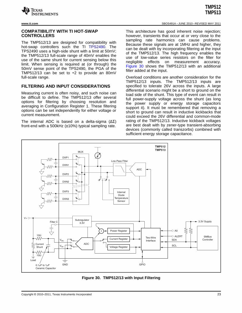
www.ti.com SBOS491A –JUNE 2010–REVISED MAY 2011
COMPATIBILITY WITH TI HOT-SWAP This architecture has good inherent noise rejection;CONTROLLERS however, transients that occur at or very close to the
sampling rate harmonics can cause problems.The TMP512/13 are designed for compatibility with Because these signals are at 1MHz and higher, theyhot-swap controllers such the TI TPS2490. The can be dealt with by incorporating filtering at the inputTPS2490 uses a high-side shunt with a limit at 50mV; of the TMP512/13. The high frequency enables thethe TMP512/13 full-scale range of 40mV enables the use of low-value series resistors on the filter foruse of the same shunt for current sensing below this negligible effects on measurement accuracy.limit. When sensing is required at (or through) the Figure 30 shows the TMP512/13 with an additional50mV sense point of the TPS2490, the PGA of the filter added at the input.TMP512/13 can be set to ÷2 to provide an 80mVfull-scale range. Overload conditions are another consideration for the
TMP512/13 inputs. The TMP512/13 inputs arespecified to tolerate 26V across the inputs. A largeFILTERING AND INPUT CONSIDERATIONSdifferential scenario might be a short to ground on the
Measuring current is often noisy, and such noise can load side of the shunt. This type of event can result inbe difficult to define. The TMP512/13 offer several full power-supply voltage across the shunt (as longoptions for filtering by choosing resolution and the power supply or energy storage capacitorsaveraging in Configuration Register 1. These filtering support it). It must be remembered that removing aoptions can be set independently for either voltage or short to ground can result in inductive kickbacks thatcurrent measurement. could exceed the 26V differential and common-mode
rating of the TMP512/13. Inductive kickback voltagesThe internal ADC is based on a delta-sigma (ΔΣ)are best dealt with by zener-type transient-absorbingfront-end with a 500kHz (±10%) typical sampling rate.devices (commonly called transzorbs) combined withsufficient energy storage capacitance.
Figure 30. TMP512/13 with Input Filtering
Copyright © 2010–2011, Texas Instruments Incorporated 23
TMP512TMP513
SBOS491A –JUNE 2010–REVISED MAY 2011 www.ti.com
In applications that do not have large energy storage not generate an Acknowledge and continues to holdelectrolytics on one or both sides of the shunt, an the ALERT line low until the interrupt is cleared.input overstress condition may result from an Successful completion of the read alert responseexcessive dV/dt of the voltage applied to the input. A protocol clears the SMBus ALERT pin, provided thathard physical short is the most likely cause of this the condition causing the alert no longer exists. Theevent, particularly in applications with no large SMBus Alert flag is cleared separately by eitherelectrolytics present. This problem occurs because an reading the Status Register or by disabling theexcessive dV/dt can activate the ESD protection in SMBus Alert function.the TMP512/13 in systems where large currents are
The Status Register flags indicate which (if any) ofavailable. Testing has demonstrated that the additionthe watchdogs have been activated. After power-onof 10Ω resistors in series with each input of thereset (POR), the normal state of all flag bits is '0',TMP512/13 sufficiently protects the inputs againstassuming that no alarm conditions exist.dV/dt failure up to the 26V rating of the TMP512/13.
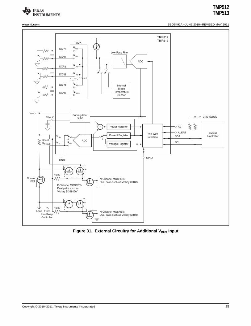
These resistors have no significant effect onEXTERNAL CIRCUITRY FOR ADDITIONALaccuracy.VBUS INPUT
SMBus ALERT RESPONSE The TMP512/13 GPIO can be used to control anexternal circuit to switch the VBUS measurement to anThe SMBus alert response functions only when thealternate location. Switching is most often done toAlert pin is active and in latch mode (03h, bit 0 = 1);perform bus voltage measurements on the oppositesee Figure 26. The ALERT interrupt output signal isside of a MOSFET switch in series with the shuntlatched and can be cleared only by either reading theresistor.Status Register or by successfully responding to an
alert response address. If the fault is still present, the Consideration must be given to the typical 20μA inputALERT pin re-asserts. Asserting the ALERT pin does current of each TMP512/13 input, along with thenot halt automatic conversions that are already in 320kΩ impedance present at the VIN– input where theprogress. The ALERT output pin is open-drain, bus voltage is measured. These effects can createallowing multiple devices to share a common interrupt errors through the resistance of any externalline. switching method used. The easiest way to avoid
these errors is by reducing this resistance to aThe TMP512/13 respond to the SMBus alertminimum; select switching MOSFETs with the lowestresponse address, an interrupt pointer return-addresspossible RDS(on) values.feature. The SMBus alert response interrupt pointer
provides quick fault identification for simple slave The circuit shown in Figure 31 uses MOSFET pairs todevices. When an ALERT occurs, the master can reduce package count. Back-to-back MOSFETs mustbroadcast the alert response slave address (0001 be used in each leg because of the built-in back100). Following this alert response, any slave devices diodes from source-to-drain. In this circuit, the normalthat generated interrupts identify themselves by connection for VIN– is at the shunt, with the optionalputting the respective addresses on the bus. voltage measurement at the output of the control
FET.The alert response can activate several differentslave devices simultaneously, similar to the two-wireGeneral Call. If more than one slave attempts torespond, bus arbitration rules apply; the device withthe lower address code wins. The losing device does
24 Copyright © 2010–2011, Texas Instruments Incorporated
´ Power Register
Current RegisterTwo-Wire
Interface
Voltage Register
ADC
GND
DXP1
DXN1
DXP2
DXN2
ADC
Low-Pass Filter
MUX
DXP3
DXN3
VIN+
VIN-
Load
Filter C
V+Subregulator
3.3V
Internal
Diode
Temperature
Sensor
A0
ALERT
SDA
SCL
SMBus
Controller
3.3V Supply
TMP512
TMP513
Shunt
RSHUNT
10kW
10kW
From
Hot-Swap
Controller
Control
FET
GPIO
N-Channel MOSFETs
Dual pairs such as Vishay SI1034
N-Channel MOSFETs
Dual pairs such as Vishay SI1034
P-Channel MOSFETs
Dual pairs such as
Vishay SI3991DV
TMP512TMP513
www.ti.com SBOS491A –JUNE 2010–REVISED MAY 2011
Figure 31. External Circuitry for Additional VBUS Input
Copyright © 2010–2011, Texas Instruments Incorporated 25
MaxPossible_I =V
RSHUNT_MAX
SHUNT
MaxPossible_I = 0.64
Minimum_LSB =Max_Expected_I
32767
Minimum_LSB = 18.311 10´-6
Maximum_LSB =Max_Expected_I
4095
Maximum_LSB = 146.520 10´-6
Cal = trunc0.04096
Current_LSB R´ SHUNT
Cal = 4096
TMP512TMP513
SBOS491A –JUNE 2010–REVISED MAY 2011 www.ti.com
PROGRAMMING THE TMP512/13 POWER MEASUREMENT ENGINE
Calibration Register and Scaling
The Calibration Register makes it possible to set the scaling of the Current and Power Registers to whatevervalues are most useful for a given application. One strategy may be to set the Calibration Register such that thelargest possible number is generated in the Current Register or Power Register at the expected full-scale point;this approach yields the highest resolution. The Calibration Register can also be selected to provide values in theCurrent and Power Registers that either provide direct decimal equivalents of the values being measured, oryield a round LSB number. After these choices have been made, the Calibration Register also offers possibilitiesfor end user system-level calibration, where the value is adjusted slightly to cancel total system error.
This section presents two examples for configuring the TMP512/13 calibration. Both examples are written so theinformation relates directly to the calibration setup found in the TMP512/13EVM software.
Calibration Example 1: Calibrating the TMP512/13 with no possibility for overflow.
NOTEThe numbers used in this example are the same used with the TMP512/13EVM softwareas shown in Figure 32.
1. Establish the following parameters:
VBUS_MAX = 32
VSHUNT_MAX = 0.32
RSHUNT = 0.52. Use Equation 6 to determine the maximum possible current .
(6)
3. Choose the desired maximum current value. This value is selected based on system expectations.
Max_Expected_I = 0.64. Calculate the possible range of current LSBs. To calculate this range, first compute a range of LSBs that is
appropriate for the design. Next, select an LSB within this range. Note that the results will have the mostresolution when the minimum LSB is selected. Typically, an LSB is selected to be the nearest round numberto the minimum LSB value.
(7)
(8)
Choose an LSB in the range: Minimum_LSB < Selected_LSB < Maximum_LSB
Current_LSB = 20 × 10–6
Note:This value was selected to be a round number near the Minimum_LSB. This selection allows forgood resolution with a rounded LSB.
5. Compute the Calibration Register value using Equation 9:
(9)
26 Copyright © 2010–2011, Texas Instruments Incorporated
Power_LSB = 20 Current_LSB
Power_LSB = 400 10´-6
Max_Current = Current_LSB 32767´
Max_Current = 0.65534
Max_ShuntVoltage = Max_Current_Before_Overflow R´ SHUNT
Max_ShuntVoltage = 0.32
MaximumPower = Max_Current_Before_Overflow V´ BUS_MAX
MaximumPower = 20.48
Corrected_Full_Scale_Cal = truncCal MeasShuntCurrent
TMP513_Current
´
Corrected_Full_Scale_Cal = 3548
TMP512TMP513
www.ti.com SBOS491A –JUNE 2010–REVISED MAY 2011
6. Calculate the Power LSB with Equation 10. Equation 10 shows a general formula; because the bus voltagemeasurement LSB is always 4mV, the power formula reduces to the calculated result.
(10)
7. Compute the maximum current and shunt voltage values (before overflow), as shown by Equation 11 andEquation 12. Note that both Equation 11 and Equation 12 involve an If - then condition:
(11)
If Max_Current ≥ MaxPossible_I thenMax_Current_Before_Overflow = MaxPossible_I
ElseMax_Current_Before_Overflow = Max_Current
End If
(Note that Max_Current is greater than MaxPossible_I in this example.)
Max_Current_Before_Overflow = 0.64
(12)
If Max_ShuntVoltage ≥ VSHUNT_MAX
Max_ShuntVoltage_Before_Overflow = VSHUNT_MAX
ElseMax_ShuntVoltage_Before_Overflow= Max_ShuntVoltage
End If(Note that Max_ShuntVoltage is greater than VSHUNT_MAX in this example.)Max_ShuntVoltage_Before_Overflow = 0.32
8. Compute the maximum power with Equation 13.
(13)
9. (Optional second Calibration step.) Compute corrected full-scale calibration value based on measuredcurrent.
TMP513_Current = 0.63484
MeaShuntCurrent = 0.55
(14)
Figure 32 illustrates how to perform the same procedure discussed in this example using the automatedTMP512/13EVM software. Note that the same numbers used in this nine-step example are used in the softwareexample. Note also that Figure 32 illustrates which results correspond to which step (for example, the informationentered in Step 1 is enclosed in a box in Figure 32 and labeled).
Copyright © 2010–2011, Texas Instruments Incorporated 27
TMP512TMP513
SBOS491A –JUNE 2010–REVISED MAY 2011 www.ti.com
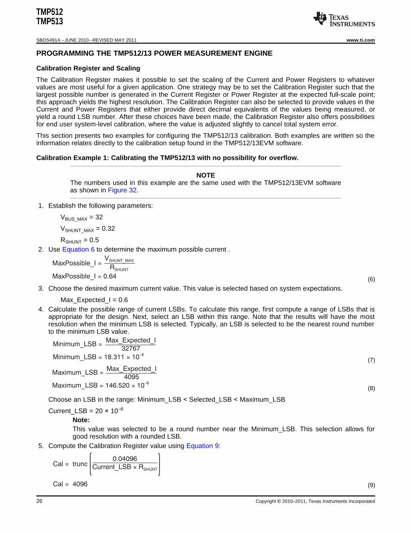
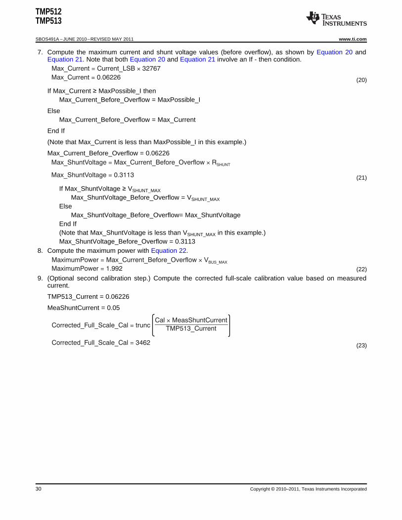
Figure 32. TMP512/513EVM Calibration Software Automatically Computes Calibration Steps 1-9
28 Copyright © 2010–2011, Texas Instruments Incorporated
MaxPossible_I =V
RSHUNT_MAX
SHUNT
MaxPossible_I = 0.064
Minimum_LSB =Max_Expected_I
32767
Minimum_LSB = 1.831 10´-6
Maximum_LSB =Max_Expected_I
4095
Maximum_LSB = 14.652 10´-6
Cal = trunc0.04096
Current_LSB R´ SHUNT
Cal = 4311
Power_LSB = 20 Current_LSB
Power_LSB = 38 10´-6
TMP512TMP513
www.ti.com SBOS491A –JUNE 2010–REVISED MAY 2011
Calibration Example 2 (Overflow Possible)
This design example uses the nine-step procedure for calibrating the TMP512/13 where overflow is possible.Figure 33 illustrates how the same procedure is performed using the automated TMP512/13EVN software. Thesame numbers used in the nine-step example are used in the software example shown in Figure 33. Note alsothat Figure 33 illustrates which results correspond to which step (for example, the information entered in Step 1is circled in Figure 33 and labeled).
1. Establish the following parameters:
VBUS_MAX = 32
VSHUNT_MAX = 0.32
RSHUNT = 52. Determine the maximum possible current using Equation 15:
(15)
3. Choose the desired maximum current value: Max_Expected_I, ≤ MaxPossible_I. This value is selectedbased on system expectations.
Max_Expected_I = 0.064. Calculate the possible range of current LSBs. This calculation is done by first computing a range of LSB's
that is appropriate for the design. Next, select an LSB withing this range. Note that the results will have themost resolution when the minimum LSB is selected. Typically, an LSB is selected to be the nearest roundnumber to the minimum LSB.
(16)
(17)
Choose an LSB in the range: Minimum_LSB < Selected_LSB < Maximum_LSB
Current_LSB = 1.9 × 10⁻⁶
Note:This value was selected to be a round number near the Minimum_LSB. This section allows for goodresolution with a rounded LSB.
5. Compute the calibration register using Equation 18:
(18)
6. Calculate the Power LSB using Equation 19. Equation 19 shows a general formula; because the bus voltagemeasurement LSB is always 4mV, the power formula reduces to calculate the result.
(19)
Copyright © 2010–2011, Texas Instruments Incorporated 29
Max_Current = Current_LSB 32767´
Max_Current = 0.06226
Max_ShuntVoltage = Max_Current_Before_Overflow R´ SHUNT
Max_ShuntVoltage = 0.3113
MaximumPower = Max_Current_Before_Overflow V´ BUS_MAX
MaximumPower = 1.992
Corrected_Full_Scale_Cal = truncCal MeasShuntCurrent
TMP513_Current
´
Corrected_Full_Scale_Cal = 3462
TMP512TMP513
SBOS491A –JUNE 2010–REVISED MAY 2011 www.ti.com
7. Compute the maximum current and shunt voltage values (before overflow), as shown by Equation 20 andEquation 21. Note that both Equation 20 and Equation 21 involve an If - then condition.
(20)
If Max_Current ≥ MaxPossible_I thenMax_Current_Before_Overflow = MaxPossible_I
ElseMax_Current_Before_Overflow = Max_Current
End If
(Note that Max_Current is less than MaxPossible_I in this example.)
Max_Current_Before_Overflow = 0.06226
(21)
If Max_ShuntVoltage ≥ VSHUNT_MAX
Max_ShuntVoltage_Before_Overflow = VSHUNT_MAX
ElseMax_ShuntVoltage_Before_Overflow= Max_ShuntVoltage
End If(Note that Max_ShuntVoltage is less than VSHUNT_MAX in this example.)Max_ShuntVoltage_Before_Overflow = 0.3113
8. Compute the maximum power with Equation 22.
(22)
9. (Optional second calibration step.) Compute the corrected full-scale calibration value based on measuredcurrent.
TMP513_Current = 0.06226
MeaShuntCurrent = 0.05
(23)
30 Copyright © 2010–2011, Texas Instruments Incorporated
TMP512TMP513
www.ti.com SBOS491A –JUNE 2010–REVISED MAY 2011
Figure 33. TMP512/513EVM Calibration Software Automatically Computes Calibration Steps 1-9
Copyright © 2010–2011, Texas Instruments Incorporated 31
TMP512TMP513
SBOS491A –JUNE 2010–REVISED MAY 2011 www.ti.com
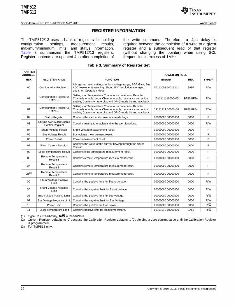
REGISTER INFORMATION
The TMP512/13 uses a bank of registers for holding the write command. Therefore, a 4μs delay isconfiguration settings, measurement results, required between the completion of a write to a givenmaximum/minimum limits, and status information. register and a subsequent read of that registerTable 3 summarizes the TMP512/13 registers. (without changing the pointer) when using SCLRegister contents are updated 4μs after completion of frequencies in excess of 1MHz.
Table 3. Summary of Register Set
POINTERADDRESS POWER-ON RESET
HEX REGISTER NAME FUNCTION BINARY HEX TYPE (1)
All-register reset, settings for bus voltage range, PGA Gain, Bus00 Configuration Register 1 ADC resolution/averaging, Shunt ADC resolution/averaging, 00111001 10011111 399F R/W
one-shot, Operation Mode.
Settings for Temperature Continuous conversion, RemoteConfiguration Register 201 Channels enable, Local Channel enable, resistance correction 1011111110000x00 BF80/BF84 R/WTMP512 enable, Conversion rate bits, and GPIO mode bit and readback.
Settings for Temperature Continuous conversion, RemoteConfiguration Register 201 Channels enable, Local Channel enable, resistance correction 11111111 10000x00 FF80/FF84 R/WTMP513 enable, Conversion rate bits, and GPIO mode bit and readback.
02 Status Register Contains the alert and conversion ready flags. 00000000 00000000 0000 R
SMBus Alert Mask/Enable03 Contains masks to enable/disable the alert functions. 00000000 00000000 0000 R/WControl Register
04 Shunt Voltage Result Shunt voltage measurement result. 00000000 00000000 0000 R
05 Bus Voltage Result Bus voltage measurement result. 00000000 00000000 0000 R
06 Power Result Power measurement result. 00000000 00000000 0000 R
Contains the value of the current flowing through the shunt07 Shunt Current Result (2) 00000000 00000000 0000 Rresistor.
08 Local Temperature Result Contains local temperature measurement result. 00000000 00000000 0000 R
Remote Temperature09 Contains remote temperature measurement result. 00000000 00000000 0000 RResult 1
Remote Temperature0A Contains remote temperature measurement result. 00000000 00000000 0000 RResult 2
Remote Temperature0B (3) Contains remote temperature measurement result. 00000000 00000000 0000 RResult 3
Shunt Voltage Positive0C Contains the positive limit for Shunt Voltage. 00000000 00000000 0000 R/WLimit
Shunt Voltage Negative0D Contains the negative limit for Shunt Voltage. 00000000 00000000 0000 R/WLimit
0E Bus Voltage Positive Limit Contains the positive limit for Bus Voltage. 00000000 00000000 0000 R/W
0F Bus Voltage Negative Limit Contains the negative limit for Bus Voltage. 00000000 00000000 0000 R/W
10 Power Limit Contains the positive limit for Power. 00000000 00000000 0000 R/W
11 Local Temperature Limit Contains positive limit for local temperature. 00101010 10000000 2A80 R/W
(1) Type: R = Read-Only, R/W = Read/Write.(2) Current Register defaults to '0' because the Calibration Register defaults to '0', yielding a zero current value until the Calibration Register
is programmed.(3) For TMP513 only.
32 Copyright © 2010–2011, Texas Instruments Incorporated
TMP512TMP513
www.ti.com SBOS491A –JUNE 2010–REVISED MAY 2011
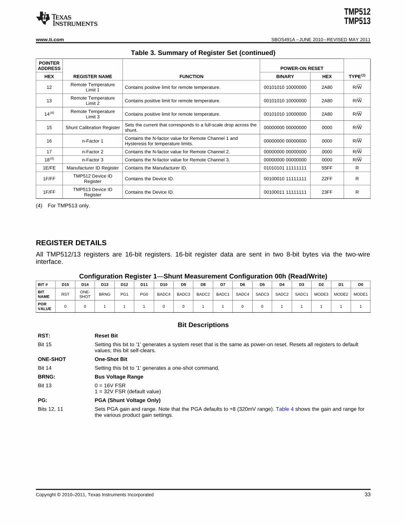
Table 3. Summary of Register Set (continued)POINTERADDRESS POWER-ON RESET
HEX REGISTER NAME FUNCTION BINARY HEX TYPE (1)
Remote Temperature12 Contains positive limit for remote temperature. 00101010 10000000 2A80 R/WLimit 1
Remote Temperature13 Contains positive limit for remote temperature. 00101010 10000000 2A80 R/WLimit 2
Remote Temperature14 (4) Contains positive limit for remote temperature. 00101010 10000000 2A80 R/WLimit 3
Sets the current that corresponds to a full-scale drop across the15 Shunt Calibration Register 00000000 00000000 0000 R/Wshunt.
Contains the N-factor value for Remote Channel 1 and16 n-Factor 1 00000000 00000000 0000 R/WHysteresis for temperature limits.
17 n-Factor 2 Contains the N-factor value for Remote Channel 2. 00000000 00000000 0000 R/W
18 (4) n-Factor 3 Contains the N-factor value for Remote Channel 3. 00000000 00000000 0000 R/W
1E/FE Manufacturer ID Register Contains the Manufacturer ID. 01010101 11111111 55FF R
TMP512 Device ID1F/FF Contains the Device ID. 00100010 11111111 22FF RRegister
TMP513 Device ID1F/FF Contains the Device ID. 00100011 11111111 23FF RRegister
(4) For TMP513 only.
space
space
REGISTER DETAILS
All TMP512/13 registers are 16-bit registers. 16-bit register data are sent in two 8-bit bytes via the two-wireinterface.
Configuration Register 1—Shunt Measurement Configuration 00h (Read/Write)BIT # D15 D14 D13 D12 D11 D10 D9 D8 D7 D6 D5 D4 D3 D2 D1 D0
BIT ONE-RST BRNG PG1 PG0 BADC4 BADC3 BADC2 BADC1 SADC4 SADC3 SADC2 SADC1 MODE3 MODE2 MODE1NAME SHOT
POR0 0 1 1 1 0 0 1 1 0 0 1 1 1 1 1VALUE
Bit Descriptions
RST: Reset Bit
Bit 15 Setting this bit to '1' generates a system reset that is the same as power-on reset. Resets all registers to defaultvalues; this bit self-clears.
ONE-SHOT One-Shot Bit
Bit 14 Setting this bit to '1' generates a one-shot command.
BRNG: Bus Voltage Range
Bit 13 0 = 16V FSR1 = 32V FSR (default value)
PG: PGA (Shunt Voltage Only)
Bits 12, 11 Sets PGA gain and range. Note that the PGA defaults to ÷8 (320mV range). Table 4 shows the gain and range forthe various product gain settings.
Copyright © 2010–2011, Texas Instruments Incorporated 33
TMP512TMP513
SBOS491A –JUNE 2010–REVISED MAY 2011 www.ti.com
Table 4. PG Bit Settings (1)
PG1 PG0 GAIN RANGE
0 0 1 ±40mV
0 1 ÷2 ±80mV
1 0 ÷4 ±160mV
1 1 ÷8 ±320mV
(1) Shaded values are default.
BADC: BADC Bus ADC Resolution/Averaging
Bits 10–7 These bits adjust the Bus ADC resolution (9-, 10-, 11-, or 12-bit) or set the number of samples used whenaveraging results for the Bus Voltage Register (05h).
SADC: SADC Shunt ADC Resolution/Averaging
Bits 6–3 These bits adjust the Shunt ADC resolution (9-, 10-, 11-, or 12-bit) or set the number of samples used whenaveraging results for the Shunt Voltage Register (04h).
BADC (Bus) and SADC (Shunt) ADC resolution/averaging and conversion time settings are shown in Table 5.
Table 5. ADC Settings (1)
ADC4 ADC3 ADC2 ADC1 MODE/SAMPLES CONVERSION TIME
0 X(2) 0 0 9-bit 105μs
0 X(2) 0 1 10-bit 185μs
0 X(2) 1 0 11-bit 345μs
0 X(2) 1 1 12-bit 665μs
1 0 0 0 12-bit 665μs
1 0 0 1 2 1.3ms
1 0 1 0 4 2.58ms
1 0 1 1 8 5.13ms
1 1 0 0 16 10.25ms
1 1 0 1 32 20.49ms
1 1 1 0 64 40.97ms
1 1 1 1 128 81.92ms
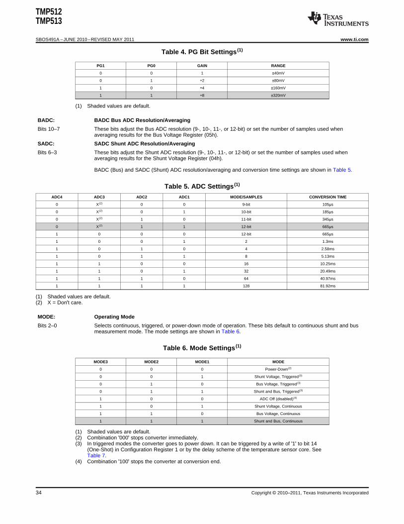
(1) Shaded values are default.(2) X = Don't care.
MODE: Operating Mode
Bits 2–0 Selects continuous, triggered, or power-down mode of operation. These bits default to continuous shunt and busmeasurement mode. The mode settings are shown in Table 6.
Table 6. Mode Settings (1)
MODE3 MODE2 MODE1 MODE
0 0 0 Power-Down (2)
0 0 1 Shunt Voltage, Triggered(3)
0 1 0 Bus Voltage, Triggered(3)
0 1 1 Shunt and Bus, Triggered(3)
1 0 0 ADC Off (disabled) (4)
1 0 1 Shunt Voltage, Continuous
1 1 0 Bus Voltage, Continuous
1 1 1 Shunt and Bus, Continuous
(1) Shaded values are default.(2) Combination '000' stops converter immediately.(3) In triggered modes the converter goes to power down. It can be triggered by a write of '1' to bit 14
(One-Shot) in Configuration Register 1 or by the delay scheme of the temperature sensor core. SeeTable 7.
(4) Combination '100' stops the converter at conversion end.
34 Copyright © 2010–2011, Texas Instruments Incorporated
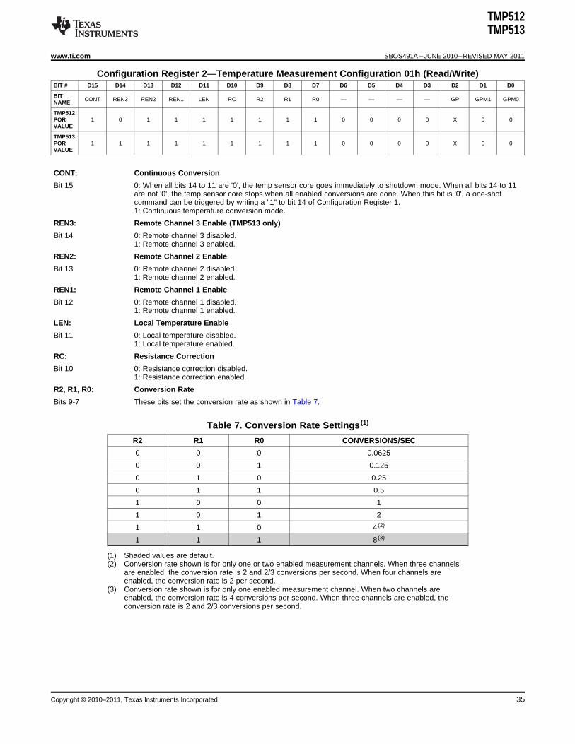
TMP512TMP513
www.ti.com SBOS491A –JUNE 2010–REVISED MAY 2011
Configuration Register 2—Temperature Measurement Configuration 01h (Read/Write)BIT # D15 D14 D13 D12 D11 D10 D9 D8 D7 D6 D5 D4 D3 D2 D1 D0
BITCONT REN3 REN2 REN1 LEN RC R2 R1 R0 — — — — GP GPM1 GPM0NAME
TMP512POR 1 0 1 1 1 1 1 1 1 0 0 0 0 X 0 0VALUE
TMP513POR 1 1 1 1 1 1 1 1 1 0 0 0 0 X 0 0VALUE
CONT: Continuous Conversion
Bit 15 0: When all bits 14 to 11 are '0', the temp sensor core goes immediately to shutdown mode. When all bits 14 to 11are not '0', the temp sensor core stops when all enabled conversions are done. When this bit is '0', a one-shotcommand can be triggered by writing a "1" to bit 14 of Configuration Register 1.1: Continuous temperature conversion mode.
REN3: Remote Channel 3 Enable (TMP513 only)
Bit 14 0: Remote channel 3 disabled.1: Remote channel 3 enabled.
REN2: Remote Channel 2 Enable
Bit 13 0: Remote channel 2 disabled.1: Remote channel 2 enabled.
REN1: Remote Channel 1 Enable
Bit 12 0: Remote channel 1 disabled.1: Remote channel 1 enabled.
LEN: Local Temperature Enable
Bit 11 0: Local temperature disabled.1: Local temperature enabled.
RC: Resistance Correction
Bit 10 0: Resistance correction disabled.1: Resistance correction enabled.
R2, R1, R0: Conversion Rate
Bits 9-7 These bits set the conversion rate as shown in Table 7.
Table 7. Conversion Rate Settings (1)
R2 R1 R0 CONVERSIONS/SEC
0 0 0 0.0625
0 0 1 0.125
0 1 0 0.25
0 1 1 0.5
1 0 0 1
1 0 1 2
1 1 0 4 (2)
1 1 1 8 (3)
(1) Shaded values are default.(2) Conversion rate shown is for only one or two enabled measurement channels. When three channels
are enabled, the conversion rate is 2 and 2/3 conversions per second. When four channels areenabled, the conversion rate is 2 per second.
(3) Conversion rate shown is for only one enabled measurement channel. When two channels areenabled, the conversion rate is 4 conversions per second. When three channels are enabled, theconversion rate is 2 and 2/3 conversions per second.
Copyright © 2010–2011, Texas Instruments Incorporated 35
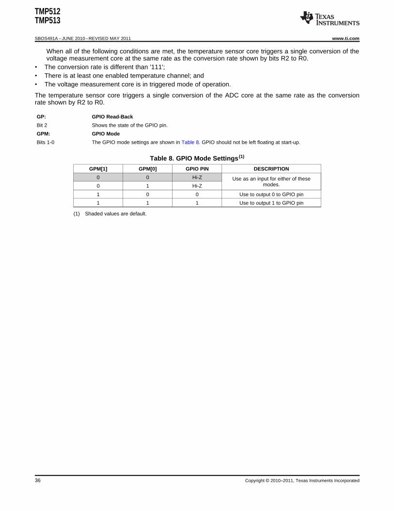
TMP512TMP513
SBOS491A –JUNE 2010–REVISED MAY 2011 www.ti.com
When all of the following conditions are met, the temperature sensor core triggers a single conversion of thevoltage measurement core at the same rate as the conversion rate shown by bits R2 to R0.
• The conversion rate is different than '111';• There is at least one enabled temperature channel; and• The voltage measurement core is in triggered mode of operation.
The temperature sensor core triggers a single conversion of the ADC core at the same rate as the conversionrate shown by R2 to R0.
GP: GPIO Read-Back
Bit 2 Shows the state of the GPIO pin.
GPM: GPIO Mode
Bits 1-0 The GPIO mode settings are shown in Table 8. GPIO should not be left floating at start-up.
Table 8. GPIO Mode Settings (1)
GPM[1] GPM[0] GPIO PIN DESCRIPTION
0 0 Hi-Z Use as an input for either of thesemodes.0 1 Hi-Z
1 0 0 Use to output 0 to GPIO pin
1 1 1 Use to output 1 to GPIO pin
(1) Shaded values are default.
36 Copyright © 2010–2011, Texas Instruments Incorporated
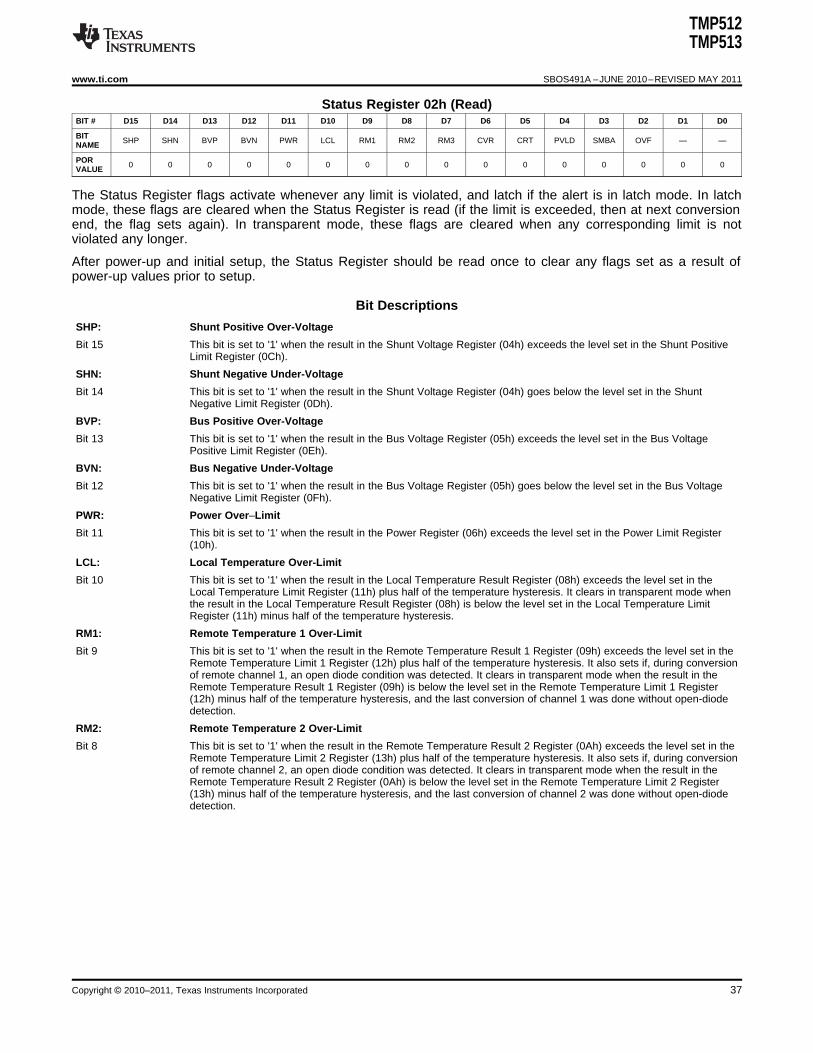
TMP512TMP513
www.ti.com SBOS491A –JUNE 2010–REVISED MAY 2011
Status Register 02h (Read)BIT # D15 D14 D13 D12 D11 D10 D9 D8 D7 D6 D5 D4 D3 D2 D1 D0
BITSHP SHN BVP BVN PWR LCL RM1 RM2 RM3 CVR CRT PVLD SMBA OVF — —NAME
POR0 0 0 0 0 0 0 0 0 0 0 0 0 0 0 0VALUE
The Status Register flags activate whenever any limit is violated, and latch if the alert is in latch mode. In latchmode, these flags are cleared when the Status Register is read (if the limit is exceeded, then at next conversionend, the flag sets again). In transparent mode, these flags are cleared when any corresponding limit is notviolated any longer.
After power-up and initial setup, the Status Register should be read once to clear any flags set as a result ofpower-up values prior to setup.
Bit Descriptions
SHP: Shunt Positive Over-Voltage
Bit 15 This bit is set to '1' when the result in the Shunt Voltage Register (04h) exceeds the level set in the Shunt PositiveLimit Register (0Ch).
SHN: Shunt Negative Under-Voltage
Bit 14 This bit is set to '1' when the result in the Shunt Voltage Register (04h) goes below the level set in the ShuntNegative Limit Register (0Dh).
BVP: Bus Positive Over-Voltage
Bit 13 This bit is set to '1' when the result in the Bus Voltage Register (05h) exceeds the level set in the Bus VoltagePositive Limit Register (0Eh).
BVN: Bus Negative Under-Voltage
Bit 12 This bit is set to '1' when the result in the Bus Voltage Register (05h) goes below the level set in the Bus VoltageNegative Limit Register (0Fh).
PWR: Power Over–Limit
Bit 11 This bit is set to '1' when the result in the Power Register (06h) exceeds the level set in the Power Limit Register(10h).
LCL: Local Temperature Over-Limit
Bit 10 This bit is set to '1' when the result in the Local Temperature Result Register (08h) exceeds the level set in theLocal Temperature Limit Register (11h) plus half of the temperature hysteresis. It clears in transparent mode whenthe result in the Local Temperature Result Register (08h) is below the level set in the Local Temperature LimitRegister (11h) minus half of the temperature hysteresis.
RM1: Remote Temperature 1 Over-Limit
Bit 9 This bit is set to '1' when the result in the Remote Temperature Result 1 Register (09h) exceeds the level set in theRemote Temperature Limit 1 Register (12h) plus half of the temperature hysteresis. It also sets if, during conversionof remote channel 1, an open diode condition was detected. It clears in transparent mode when the result in theRemote Temperature Result 1 Register (09h) is below the level set in the Remote Temperature Limit 1 Register(12h) minus half of the temperature hysteresis, and the last conversion of channel 1 was done without open-diodedetection.
RM2: Remote Temperature 2 Over-Limit
Bit 8 This bit is set to '1' when the result in the Remote Temperature Result 2 Register (0Ah) exceeds the level set in theRemote Temperature Limit 2 Register (13h) plus half of the temperature hysteresis. It also sets if, during conversionof remote channel 2, an open diode condition was detected. It clears in transparent mode when the result in theRemote Temperature Result 2 Register (0Ah) is below the level set in the Remote Temperature Limit 2 Register(13h) minus half of the temperature hysteresis, and the last conversion of channel 2 was done without open-diodedetection.
Copyright © 2010–2011, Texas Instruments Incorporated 37
TMP512TMP513
SBOS491A –JUNE 2010–REVISED MAY 2011 www.ti.com
Bit Descriptions (continued)
RM3: Remote Temperature 3 Over-Limit (TMP513 only)
Bit 7 This bit is set to '1' when the result in the Remote Temperature Result 3 Register (0Bh) exceeds the level set in theRemote Temperature Limit 3 Register (14h) plus half of the temperature hysteresis. It sets also if during conversionof remote channel 3 an open diode condition was detected. It clears in transparent mode when the result in theRemote Temperature Result 3Register (0Bh) is below the level set in the Remote Temperature Limit 3 Register(14h) minus half of the temperature hysteresis and the last conversion of channel 3 was done without open-diodedetection.
CVR: Conversion Ready
Bit 6 The Conversion Ready line is provided to help coordinate one-shot conversions for shunt voltage, bus voltage,current and power measurements. The Conversion bit is set after all conversions, averaging, and multiplicationevents are complete. Conversion Ready clears under the following conditions:
1. Writing to the One-Shot bit in Configuration Register 1.
2. Reading the Status Register.
CRT: Conversion Ready Temperature
Bit 5 The Conversion Ready Temperature line is provided to help coordinate one-shot conversions for local and remotetemperature measurements. The Conversion bit is set after all enabled channels complete the respectiveconversions. Conversion Ready Temperature clears under the following conditions:
1. Writing to the One-Shot bit in Configuration Register 1.
2. Reading the Status Register.
PVLD: Power Valid Error
Bit 4 In latch mode, this bit is set to '1' when the brown-out detect fires during a conversion. The flag sets to '1' at theconversion end. It clears by reading the Status Register.
SMBA: SMBus Alert
Bit 3 This bit is set when the Alert pin is active. When in latch mode, it clears only on reading the Status Register,disabling the SMBus Alert function, or using SMBus Alert Response. In transparent mode, it clears when thetriggering condition is not present.
OVF: Math Overflow
Bit 2 This bit is set to '1' if an arithmetic operation resulted in an overflow error. It indicates that current and power datamay be meaningless. It does not set the Alert pin.
38 Copyright © 2010–2011, Texas Instruments Incorporated
TMP512TMP513
www.ti.com SBOS491A –JUNE 2010–REVISED MAY 2011
SMBus Alert Register—Mask and Alert Control Functions 03h (Read/Write)BIT # D15 D14 D13 D12 D11 D10 D9 D8 D7 D6 D5 D4 D3 D2 D1 D0
BITSHPM SHNM BVPM BVNM PWRM LCLM R1M R2M R3M CVRM CRTM PVLM FC1 FC0 POL LATCHNAME
POR0 0 0 0 0 0 0 0 0 0 0 0 0 0 0 0VALUE
Bits D4–D15 of the SMBus Alert Register mask correspond to bits D4 to D15 of the Status Register to preventthem from initiating an SMBus Alert. It does not prevent the Status Register bit from setting. Writing a '0' to anSMBus Alert Mask bit masks it from activating the SMBus Alert. All default values are '0'.
Bit Descriptions
SHPM: Shunt Positive Over-Voltage Mask
Bit 15 0: SHP flag in Status Register cannot activate Alert pin.
1: SHP flag (when set to '1') in Status Register activates Alert pin.
SHNM: Shunt Negative Under-Voltage Mask
Bit 14 0: SHN flag in Status Register cannot activate Alert pin.
1: SHN flag (when set to '1') in Status Register activates Alert pin.
BVPM: Bus Voltage Positive Over-Voltage Mask
Bit 13 0: BVP flag in Status Register cannot activate Alert pin.
1: BVP flag (when set to '1') in Status Register activates Alert pin.
BVNM: Bus Voltage Negative Under-Voltage Mask
Bit 12 0: BVN flag in Status Register cannot activate Alert pin.
1: BVN flag (when set to '1') in Status Register activates Alert pin.
PWRM: Power Over-Limit Mask
Bit 11 0: PWR flag in Status Register cannot activate Alert pin.
1: PWR flag (when set to '1') in Status Register activates Alert pin.
LCLM: Local Temperature Over-Limit Mask
Bit 10 0: LCL flag in Status Register cannot activate Alert pin.
1: LCL flag (when set to '1') in Status Register activates Alert pin.
R1M: Remote Temperature1 Over-Limit Mask
Bit 9 0: RM1 flag in Status Register cannot activate Alert pin.
1: RM1 flag (when set to '1') in Status Register activates Alert pin.
R2M: Remote Temperature2 Over-Limit Mask
Bit 8 0: RM2 flag in Status Register cannot activate Alert pin.
1: RM2 flag (when set to '1') in Status Register activates Alert pin.
R3M: Remote Temperature3 Over-Limit Mask (TMP513 only)
Bit 7 0: RM3 flag in Status Register cannot activate Alert pin.
1: RM3 flag (when set to '1') in Status Register activates Alert pin.
CVRM: Conversion Ready Mask
Bit 6 0: CVR flag in Status Register cannot activate Alert pin.
1: CVR flag (when set to '1') in Status Register activates Alert pin.
CRTM: Conversion Ready Temperature Mask
Bit 5 0: CRT flag in Status Register cannot activate Alert pin.
1: CRT flag (when set to '1') in Status Register activates Alert pin.
PVLM: Power Valid Limit Mask
Bit 4 0: PVLD flag in Status Register cannot activate Alert pin.
1: PVLD flag (when set to '1') in Status Register activates Alert pin.
Copyright © 2010–2011, Texas Instruments Incorporated 39
TMP512TMP513
SBOS491A –JUNE 2010–REVISED MAY 2011 www.ti.com
Bit Descriptions (continued)
FC0, FC1 Fault Count Control Bits
The Fault Count Control Bits affect flags in SMBus Alert Register bits D15-D7.
Bit 3, 2 00: These flags are activated after the first conversion result with a violated limit.
01: These flags are activated after the second consecutive conversion result with a violated limit.
10: These flags are activated after the fourth consecutive conversion result with a violated limit.
11: These flags are activated after the eighth consecutive conversion result with a violated limit.
POL: Alert Polarity
Bit 1 0: Alert pin is active low.
1: Alert pin is active high.
LATCH: Alert Mode of Operation
Bit 0 0: Alert pin works in transparent mode. The SMB alert response function does not function. Alert is deassertedwhen the triggering condition goes away.
1: Alert pin works in latch mode. The SMB alert response function functions when Alert pin is active. Alert willremain asserted even if the triggering condition goes away. Alert can be deasserted by reading the Status register(02h), using the SMBus Alert response function, resetting the part, or by disabling the alert function using the maskbits.
40 Copyright © 2010–2011, Texas Instruments Incorporated
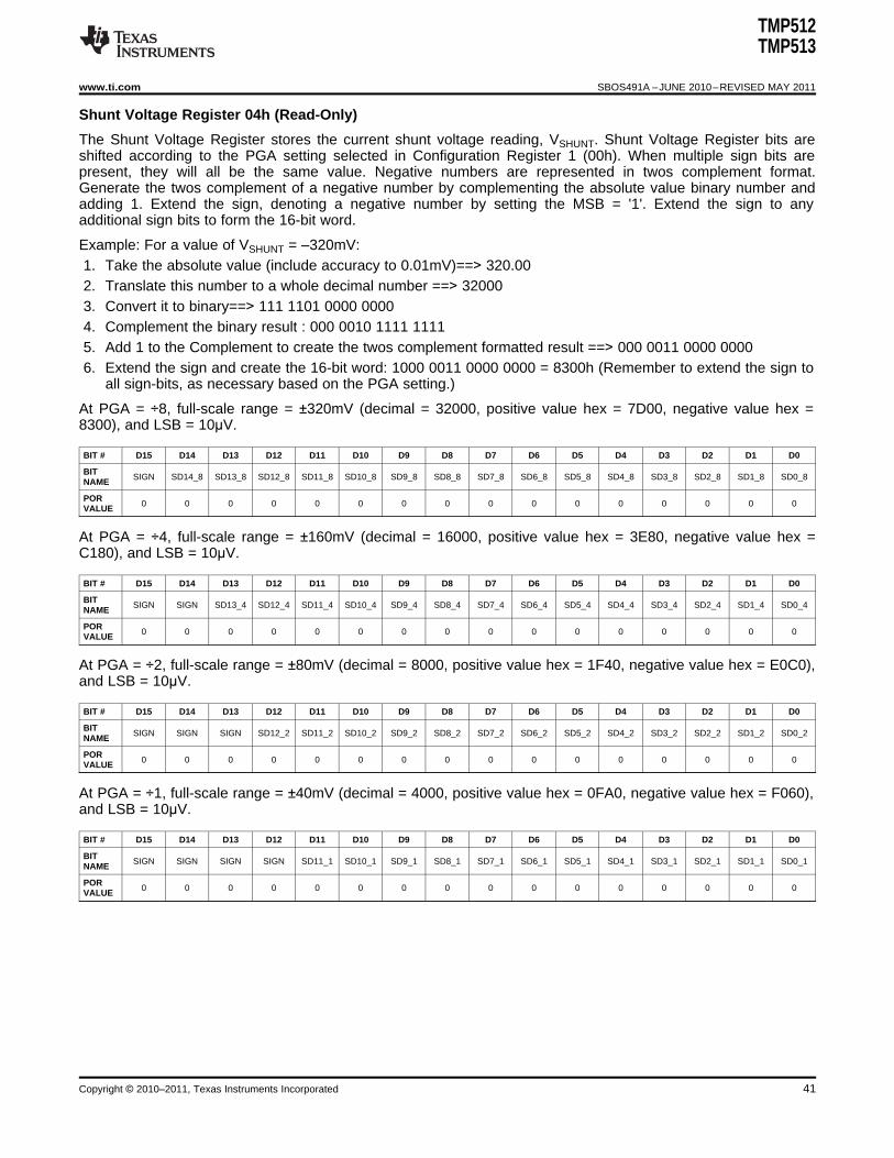
TMP512TMP513
www.ti.com SBOS491A –JUNE 2010–REVISED MAY 2011
Shunt Voltage Register 04h (Read-Only)
The Shunt Voltage Register stores the current shunt voltage reading, VSHUNT. Shunt Voltage Register bits areshifted according to the PGA setting selected in Configuration Register 1 (00h). When multiple sign bits arepresent, they will all be the same value. Negative numbers are represented in twos complement format.Generate the twos complement of a negative number by complementing the absolute value binary number andadding 1. Extend the sign, denoting a negative number by setting the MSB = '1'. Extend the sign to anyadditional sign bits to form the 16-bit word.
Example: For a value of VSHUNT = –320mV:1. Take the absolute value (include accuracy to 0.01mV)==> 320.002. Translate this number to a whole decimal number ==> 320003. Convert it to binary==> 111 1101 0000 00004. Complement the binary result : 000 0010 1111 11115. Add 1 to the Complement to create the twos complement formatted result ==> 000 0011 0000 00006. Extend the sign and create the 16-bit word: 1000 0011 0000 0000 = 8300h (Remember to extend the sign to
all sign-bits, as necessary based on the PGA setting.)
At PGA = ÷8, full-scale range = ±320mV (decimal = 32000, positive value hex = 7D00, negative value hex =8300), and LSB = 10μV.
BIT # D15 D14 D13 D12 D11 D10 D9 D8 D7 D6 D5 D4 D3 D2 D1 D0
BITSIGN SD14_8 SD13_8 SD12_8 SD11_8 SD10_8 SD9_8 SD8_8 SD7_8 SD6_8 SD5_8 SD4_8 SD3_8 SD2_8 SD1_8 SD0_8NAME
POR0 0 0 0 0 0 0 0 0 0 0 0 0 0 0 0VALUE
At PGA = ÷4, full-scale range = ±160mV (decimal = 16000, positive value hex = 3E80, negative value hex =C180), and LSB = 10μV.
BIT # D15 D14 D13 D12 D11 D10 D9 D8 D7 D6 D5 D4 D3 D2 D1 D0
BITSIGN SIGN SD13_4 SD12_4 SD11_4 SD10_4 SD9_4 SD8_4 SD7_4 SD6_4 SD5_4 SD4_4 SD3_4 SD2_4 SD1_4 SD0_4NAME
POR0 0 0 0 0 0 0 0 0 0 0 0 0 0 0 0VALUE
At PGA = ÷2, full-scale range = ±80mV (decimal = 8000, positive value hex = 1F40, negative value hex = E0C0),and LSB = 10μV.
BIT # D15 D14 D13 D12 D11 D10 D9 D8 D7 D6 D5 D4 D3 D2 D1 D0
BITSIGN SIGN SIGN SD12_2 SD11_2 SD10_2 SD9_2 SD8_2 SD7_2 SD6_2 SD5_2 SD4_2 SD3_2 SD2_2 SD1_2 SD0_2NAME
POR0 0 0 0 0 0 0 0 0 0 0 0 0 0 0 0VALUE
At PGA = ÷1, full-scale range = ±40mV (decimal = 4000, positive value hex = 0FA0, negative value hex = F060),and LSB = 10μV.
BIT # D15 D14 D13 D12 D11 D10 D9 D8 D7 D6 D5 D4 D3 D2 D1 D0
BITSIGN SIGN SIGN SIGN SD11_1 SD10_1 SD9_1 SD8_1 SD7_1 SD6_1 SD5_1 SD4_1 SD3_1 SD2_1 SD1_1 SD0_1NAME
POR0 0 0 0 0 0 0 0 0 0 0 0 0 0 0 0VALUE
Copyright © 2010–2011, Texas Instruments Incorporated 41
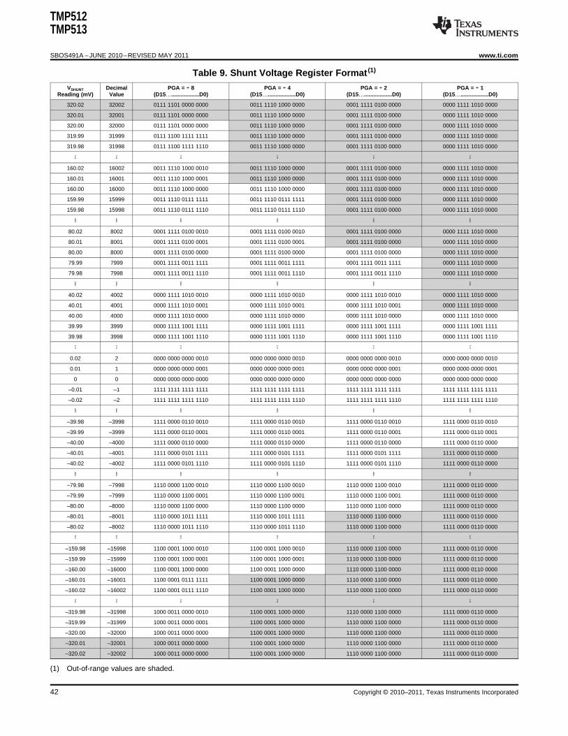
TMP512TMP513
SBOS491A –JUNE 2010–REVISED MAY 2011 www.ti.com
Table 9. Shunt Voltage Register Format (1)
VSHUNT Decimal PGA = ÷ 8 PGA = ÷ 4 PGA = ÷ 2 PGA = ÷ 1Reading (mV) Value (D15…..................D0) (D15…..................D0) (D15…..................D0) (D15…..................D0)
320.02 32002 0111 1101 0000 0000 0011 1110 1000 0000 0001 1111 0100 0000 0000 1111 1010 0000
320.01 32001 0111 1101 0000 0000 0011 1110 1000 0000 0001 1111 0100 0000 0000 1111 1010 0000
320.00 32000 0111 1101 0000 0000 0011 1110 1000 0000 0001 1111 0100 0000 0000 1111 1010 0000
319.99 31999 0111 1100 1111 1111 0011 1110 1000 0000 0001 1111 0100 0000 0000 1111 1010 0000
319.98 31998 0111 1100 1111 1110 0011 1110 1000 0000 0001 1111 0100 0000 0000 1111 1010 0000
160.02 16002 0011 1110 1000 0010 0011 1110 1000 0000 0001 1111 0100 0000 0000 1111 1010 0000
160.01 16001 0011 1110 1000 0001 0011 1110 1000 0000 0001 1111 0100 0000 0000 1111 1010 0000
160.00 16000 0011 1110 1000 0000 0011 1110 1000 0000 0001 1111 0100 0000 0000 1111 1010 0000
159.99 15999 0011 1110 0111 1111 0011 1110 0111 1111 0001 1111 0100 0000 0000 1111 1010 0000
159.98 15998 0011 1110 0111 1110 0011 1110 0111 1110 0001 1111 0100 0000 0000 1111 1010 0000
80.02 8002 0001 1111 0100 0010 0001 1111 0100 0010 0001 1111 0100 0000 0000 1111 1010 0000
80.01 8001 0001 1111 0100 0001 0001 1111 0100 0001 0001 1111 0100 0000 0000 1111 1010 0000
80.00 8000 0001 1111 0100 0000 0001 1111 0100 0000 0001 1111 0100 0000 0000 1111 1010 0000
79.99 7999 0001 1111 0011 1111 0001 1111 0011 1111 0001 1111 0011 1111 0000 1111 1010 0000
79.98 7998 0001 1111 0011 1110 0001 1111 0011 1110 0001 1111 0011 1110 0000 1111 1010 0000
40.02 4002 0000 1111 1010 0010 0000 1111 1010 0010 0000 1111 1010 0010 0000 1111 1010 0000
40.01 4001 0000 1111 1010 0001 0000 1111 1010 0001 0000 1111 1010 0001 0000 1111 1010 0000
40.00 4000 0000 1111 1010 0000 0000 1111 1010 0000 0000 1111 1010 0000 0000 1111 1010 0000
39.99 3999 0000 1111 1001 1111 0000 1111 1001 1111 0000 1111 1001 1111 0000 1111 1001 1111
39.98 3998 0000 1111 1001 1110 0000 1111 1001 1110 0000 1111 1001 1110 0000 1111 1001 1110
0.02 2 0000 0000 0000 0010 0000 0000 0000 0010 0000 0000 0000 0010 0000 0000 0000 0010
0.01 1 0000 0000 0000 0001 0000 0000 0000 0001 0000 0000 0000 0001 0000 0000 0000 0001
0 0 0000 0000 0000 0000 0000 0000 0000 0000 0000 0000 0000 0000 0000 0000 0000 0000
–0.01 –1 1111 1111 1111 1111 1111 1111 1111 1111 1111 1111 1111 1111 1111 1111 1111 1111
–0.02 –2 1111 1111 1111 1110 1111 1111 1111 1110 1111 1111 1111 1110 1111 1111 1111 1110
–39.98 –3998 1111 0000 0110 0010 1111 0000 0110 0010 1111 0000 0110 0010 1111 0000 0110 0010
–39.99 –3999 1111 0000 0110 0001 1111 0000 0110 0001 1111 0000 0110 0001 1111 0000 0110 0001
–40.00 –4000 1111 0000 0110 0000 1111 0000 0110 0000 1111 0000 0110 0000 1111 0000 0110 0000
–40.01 –4001 1111 0000 0101 1111 1111 0000 0101 1111 1111 0000 0101 1111 1111 0000 0110 0000
–40.02 –4002 1111 0000 0101 1110 1111 0000 0101 1110 1111 0000 0101 1110 1111 0000 0110 0000
–79.98 –7998 1110 0000 1100 0010 1110 0000 1100 0010 1110 0000 1100 0010 1111 0000 0110 0000
–79.99 –7999 1110 0000 1100 0001 1110 0000 1100 0001 1110 0000 1100 0001 1111 0000 0110 0000
–80.00 –8000 1110 0000 1100 0000 1110 0000 1100 0000 1110 0000 1100 0000 1111 0000 0110 0000
–80.01 –8001 1110 0000 1011 1111 1110 0000 1011 1111 1110 0000 1100 0000 1111 0000 0110 0000
–80.02 –8002 1110 0000 1011 1110 1110 0000 1011 1110 1110 0000 1100 0000 1111 0000 0110 0000
–159.98 –15998 1100 0001 1000 0010 1100 0001 1000 0010 1110 0000 1100 0000 1111 0000 0110 0000
–159.99 –15999 1100 0001 1000 0001 1100 0001 1000 0001 1110 0000 1100 0000 1111 0000 0110 0000
–160.00 –16000 1100 0001 1000 0000 1100 0001 1000 0000 1110 0000 1100 0000 1111 0000 0110 0000
–160.01 –16001 1100 0001 0111 1111 1100 0001 1000 0000 1110 0000 1100 0000 1111 0000 0110 0000
–160.02 –16002 1100 0001 0111 1110 1100 0001 1000 0000 1110 0000 1100 0000 1111 0000 0110 0000
–319.98 –31998 1000 0011 0000 0010 1100 0001 1000 0000 1110 0000 1100 0000 1111 0000 0110 0000
–319.99 –31999 1000 0011 0000 0001 1100 0001 1000 0000 1110 0000 1100 0000 1111 0000 0110 0000
–320.00 –32000 1000 0011 0000 0000 1100 0001 1000 0000 1110 0000 1100 0000 1111 0000 0110 0000
–320.01 –32001 1000 0011 0000 0000 1100 0001 1000 0000 1110 0000 1100 0000 1111 0000 0110 0000
–320.02 –32002 1000 0011 0000 0000 1100 0001 1000 0000 1110 0000 1100 0000 1111 0000 0110 0000
(1) Out-of-range values are shaded.
42 Copyright © 2010–2011, Texas Instruments Incorporated
Power =Current BusVoltage´
5000
Current =ShuntVoltage Calibration Register´
4096
TMP512TMP513
www.ti.com SBOS491A –JUNE 2010–REVISED MAY 2011
Bus Voltage Register 05h (Read-Only)
The Bus Voltage Register stores the most recent bus voltage reading, VBUS.
At full-scale range = 32V (decimal = 8000, hex = 1F40), and LSB = 4mV.
BIT # D15 D14 D13 D12 D11 D10 D9 D8 D7 D6 D5 D4 D3 D2 D1 D0
BITBD12 BD11 BD10 BD9 BD8 BD7 BD6 BD5 BD4 BD3 BD2 BD1 BD0 — — —NAME
POR0 0 0 0 0 0 0 0 0 0 0 0 0 0 0 0VALUE
At full-scale range = 16V (decimal = 4000, hex = 0FA0), and LSB = 4mV.
BIT # D15 D14 D13 D12 D11 D10 D9 D8 D7 D6 D5 D4 D3 D2 D1 D0
BIT0 BD11 BD10 BD9 BD8 BD7 BD6 BD5 BD4 BD3 BD2 BD1 BD0 — — —NAME
POR0 0 0 0 0 0 0 0 0 0 0 0 0 0 0 0VALUE
Power Register 06h (Read-Only)
Full-scale range and LSB are set by the Calibration Register. See the Programming the TMP512/13 PowerMeasurement Engine section.
BIT # D15 D14 D13 D12 D11 D10 D9 D8 D7 D6 D5 D4 D3 D2 D1 D0
BITPD15 PD14 PD13 PD12 PD11 PD10 PD9 PD8 PD7 PD6 PD5 PD4 PD3 PD2 PD1 PD0NAME
POR0 0 0 0 0 0 0 0 0 0 0 0 0 0 0 0VALUE
The Power Register records power in watts by multiplying the values of the current with the value of the busvoltage according to the equation:
Current Register 07h (Read-Only)
Full-scale range and LSB depend on the value entered in the Calibration Register. See the Programming theTMP512/13 Power Measurement Engine section. Negative values are stored in twos complement format.
BIT # D15 D14 D13 D12 D11 D10 D9 D8 D7 D6 D5 D4 D3 D2 D1 D0
BITCSIGN CD14 CD13 CD12 CD11 CD10 CD9 CD8 CD7 CD6 CD5 CD4 CD3 CD2 CD1 CD0NAME
POR0 0 0 0 0 0 0 0 0 0 0 0 0 0 0 0VALUE
The value of the Current Register is calculated by multiplying the value in the Shunt Voltage Register with thevalue in the Calibration Register according to the equation:
Copyright © 2010–2011, Texas Instruments Incorporated 43
TMP512TMP513
SBOS491A –JUNE 2010–REVISED MAY 2011 www.ti.com
Local Temperature Result Register 08h (Read-Only)
BIT # D15 D14 D13 D12 D11 D10 D9 D8 D7 D6 D5 D4 D3 D2 D1 D0
BITT12 T11 T10 T9 T8 T7 T6 T5 T4 T3 T2 T1 T0 — PVLD —NAME
POR0 0 0 0 0 0 0 0 0 0 0 0 0 0 0 0VALUE
The data format is 13 bits, 0.0625°C per bit. Full-scale allows display up to ±256°C.
T12–T0: Temperature Result
Bits 15-3 Shows the temperature result according to the format shown in Table 10.
Table 10. 13-Bit Temperature Data Format
TEMPERATURE (°C) DIGITAL OUTPUT (BINARY) HEX
150 0 1001 0110 0000 0960
128 0 1000 0000 0000 0800
127.9375 0 0111 1111 1111 07FF
100 0 0110 0100 0000 0640
80 0 0101 0000 0000 0500
75 0 0100 1011 0000 04B0
50 0 0011 0010 0000 0320
25 0 0001 1001 0000 0190
0.25 0 0000 0000 0100 0004
0 0 0000 0000 0000 0000
–0.25 1 1111 1111 1100 1FFC
–25 1 1110 0111 0000 1E70
–55 1 1100 1001 0000 1C90
For positive temperatures (for example, +50°C):
Twos complement is not performed on positive numbers. Therefore, simply convert the number to binary codewith the 13-bit, left-justified format, and MSB = 0 to denote a positive sign.
Example: (+50°C)/(0.0625°C/count) = 800 = 320h = 0011 0010 0000
For negative temperatures (for example, –25°C):
Generate the twos complement of a negative number by complementing the absolute value binary number andadding 1. Denote a negative number with MSB = 1.
Example: (–25°C)/(0.0625°C/count) = 400 = 190h = 0001 1001 0000
Twos complement format: 1110 0110 1111 + 1 = 1110 0111 0000
PVLD Power Valid Flag
Bit 1 This bit is the power valid flag.
The TMP512/13 do not start a temperature conversion if the power supply is not valid. If the voltage is less than2.7V during a conversion, the PVLD bit is set to '1' and the temperature result may be incorrect.
44 Copyright © 2010–2011, Texas Instruments Incorporated
TMP512TMP513
www.ti.com SBOS491A –JUNE 2010–REVISED MAY 2011
Remote Temperature Result 1 Register 09h, Remote Temperature Result 2 Register 0Ah, RemoteTemperature Result 3 Register (TMP513 Only) 0Bh (Read-Only)
BIT # D15 D14 D13 D12 D11 D10 D9 D8 D7 D6 D5 D4 D3 D2 D1 D0
BITRT12 RT11 RT10 RT9 RT8 RT7 RT6 RT5 RT4 RT3 RT2 RT1 RT0 — PVLD DONAME
POR0 0 0 0 0 0 0 0 0 0 0 0 0 0 0 0VALUE
The data format is 13 bits, 0.0625°C per bit. Full-scale allows display up to ±256°C.
RT12–RT0: Remote Temperature Result
Bits 3-15 Shows the remote temperature measurement result.
PVLD Power Valid Flag
Bit 1 This bit is the power valid flag.
The TMP512/13 do not start a temperature conversion if the power supply is not valid. If the voltage is less than2.7V during a conversion, the PVLD bit is set to '1' and the temperature result may be incorrect.
DO Diode Open Flag
Bit 0 This bit is the diode open flag.
If the Remote Channels are open during a conversion, then Diode Open bit is set at the end of the conversion.
Shunt Positive Limit Register 0Ch (Read/Write)
At full-scale range = ±320mV, 15-bit + sign, LSB = 10μV (decimal = 32000, positive value hex = 7D00, negativevalue hex = 8300).
BIT # D15 D14 D13 D12 D11 D10 D9 D8 D7 D6 D5 D4 D3 D2 D1 D0
BIT SWPSWP14 SWP13 SWP12 SWP11 SWP10 SWP9 SWP8 SWP7 SWP6 SWP5 SWP4 SWP3 SWP2 SWP1 SWP0NAME SIGN
POR0 0 0 0 0 0 0 0 0 0 0 0 0 0 0 0VALUE
Shunt Negative Limit Register 0Dh (Read/Write)
At full-scale range = ±320mV (decimal = 32000, positive value hex = 7D00, negative value hex = 8300). 15 bit +sign, LSB = 10μV.
BIT # D15 D14 D13 D12 D11 D10 D9 D8 D7 D6 D5 D4 D3 D2 D1 D0
BIT SWNSWN14 SWN13 SWN12 SWN11 SWN10 SWN9 SWN8 SWN7 SWN6 SWN5 SWN4 SWN3 SWN2 SWN1 SWN0NAME SIGN
POR0 0 0 0 0 0 0 0 0 0 0 0 0 0 0 0VALUE
Bus Voltage Positive Limit Register 0Eh (Read/Write)
At full-scale range = 32V (decimal = 8000, hex = 1F40), and LSB = 4mV.
BIT # D15 D14 D13 D12 D11 D10 D9 D8 D7 D6 D5 D4 D3 D2 D1 D0
BITBWU12 BWU11 BWU10 BWU9 BWU8 BWU7 BWU6 BWU5 BWU4 BWU3 BWU2 BWU1 BWU0 — — —NAME
POR0 0 0 0 0 0 0 0 0 0 0 0 0 0 0 0VALUE
Copyright © 2010–2011, Texas Instruments Incorporated 45
TMP512TMP513
SBOS491A –JUNE 2010–REVISED MAY 2011 www.ti.com
Bus Voltage Negative Limit Register 0Fh (Read/Write)
At full-scale range = 32V (decimal = 8000, hex = 1F40), and LSB = 4mV.
BIT # D15 D14 D13 D12 D11 D10 D9 D8 D7 D6 D5 D4 D3 D2 D1 D0
BITBUO12 BUO11 BUO10 BUO9 BUO8 BUO7 BUO6 BUO5 BUO4 BUO3 BUO2 BUO1 BUO0 — — —NAME
POR0 0 0 0 0 0 0 0 0 0 0 0 0 0 0 0VALUE
Power Limit Register 10h (Read/Write)
At full-scale range, same as the Power Register (06h).
BIT # D15 D14 D13 D12 D11 D10 D9 D8 D7 D6 D5 D4 D3 D2 D1 D0
BITPW15 PW14 PW13 PW12 PW11 PW10 PW9 PW8 PW7 PW6 PW5 PW4 PW3 PW2 PW1 PW0NAME
POR0 0 0 0 0 0 0 0 0 0 0 0 0 0 0 0VALUE
Local Temperature Limit Register 11h, Remote Temperature Limit 1 Register 12h, Remote TemperatureLimit 2 Register 13h, Remote Temperature Limit 3 Register 14h (TMP513 Only) (Read/Write)
BIT # D15 D14 D13 D12 D11 D10 D9 D8 D7 D6 D5 D4 D3 D2 D1 D0
BITTH12 TH11 TH10 TH9 TH8 TH7 TH6 TH5 TH4 TH3 TH2 TH1 TH0 — — —NAME
POR0 0 1 0 1 0 1 0 1 0 0 0 0 0 0 0VALUE
The data format is 13 bits.
TH12–TH0: Temperature Limit
Bits 15-3 Shows the temperature limit.
Shunt Calibration Register 15h (Read/Write)
Current and power calibration are set in the Calibration Register. Note that bit D0 is not used in the calculation.This register sets the current that corresponds to a full-scale drop across the shunt. Full-scale range and the LSBof the current and power measurement depend on the value entered in this register. See the Programming theTMP512/13 Power Measurement Engine section. This register is suitable for use in overall system calibration.Note that the '0' POR values are all default.
BIT # D15 D14 D13 D12 D11 D10 D9 D8 D7 D6 D5 D4 D3 D2 D1 D0 (1)
BITFS15 FS14 FS13 FS12 FS11 FS10 FS9 FS8 FS7 FS6 FS5 FS4 FS3 FS2 FS1 FS0NAME
POR0 0 0 0 0 0 0 0 0 0 0 0 0 0 0 0VALUE
(1) D0 is a void bit and is always '0'. It is not possible to write a '1' to D0.
46 Copyright © 2010–2011, Texas Instruments Incorporated
TMP512TMP513
www.ti.com SBOS491A –JUNE 2010–REVISED MAY 2011
n-Factor 1 Register 16h (Read/Write)
BIT # D15 D14 D13 D12 D11 D10 D9 D8 D7 D6 D5 D4 D3 D2 D1 D0
BITNF7 NF6 NF5 NF4 NF3 NF2 NF1 NF0 HST7 HST6 HST5 HST4 HST3 HST2 HST1 HST0NAME
POR0 0 0 0 0 0 0 0 0 0 0 0 0 0 0 0VALUE
NF7–NF0: n-Factor Bits
Bits 15-8 Shows the n-factor for Channel 1 according to the range indicated in Table 11.
Table 11. n-Factor Range (1)
NADJUST
BINARY HEX DECIMAL n
0111 1111 7F 127 1.747977
0000 1010 0A 10 1.042759
0000 1000 08 8 1.035616
0000 0110 06 6 1.028571
0000 0100 04 4 1.021622
0000 0010 02 2 1.014765
0000 0001 01 1 1.011371
0000 0000 00 0 1.008
1111 1111 FF –1 1.004651
1111 1110 FE –2 1.001325
1111 1100 FC –4 0.994737
1111 1010 FA –6 0.988235
1111 1000 F8 –8 0.981818
1111 0110 F6 –10 0.975484
1000 0000 80 –128 0.706542
(1) Shaded values are default.
HST7–HST0: Hysteresis Register Bits
Bits 7-0 The hysteresis register is binary coded. 1LSB is equal to 0.5°C, so the possible hysteresis range is 0°C to 127.5°C.
n-Factor 2 Register 17h (Read/Write)
BIT # D15 D14 D13 D12 D11 D10 D9 D8 D7 D6 D5 D4 D3 D2 D1 D0
BITNF7 NF6 NF5 NF4 NF3 NF2 NF1 NF0 — — — — — — — —NAME
POR0 0 0 0 0 0 0 0 0 0 0 0 0 0 0 0VALUE
NF7–NF0: n-Factor Bits
Bits 15-8 Shows the n-factor for Channel 2 according to the range indicated in Table 11.
n-Factor 3 Register 18h (TMP513 Only) (Read/Write)
BIT # D15 D14 D13 D12 D11 D10 D9 D8 D7 D6 D5 D4 D3 D2 D1 D0
BITNF7 NF6 NF5 NF4 NF3 NF2 NF1 NF0 — — — — — — — —NAME
POR0 0 0 0 0 0 0 0 0 0 0 0 0 0 0 0VALUE
NF7–NF0: n-Factor Bits
Bits 15-8 Shows the n-factor for Channel 3 according to the range indicated in Table 11.
Copyright © 2010–2011, Texas Instruments Incorporated 47
TMP512TMP513
SBOS491A –JUNE 2010–REVISED MAY 2011 www.ti.com
Manufacturer ID Register 1Eh and FEh (Read-Only)
BIT # D15 D14 D13 D12 D11 D10 D9 D8 D7 D6 D5 D4 D3 D2 D1 D0
BITID7 ID6 ID5 ID4 ID3 ID2 ID1 ID0 — — — — — — — —NAME
POR0 1 0 1 0 1 0 1 1 1 1 1 1 1 1 1VALUE
ID7–ID0: Identification Register Bits
Bits 15-8 These bits provide the manufacturer ID.
Device ID Register 1Fh and FFh (Read-Only)
BIT # D15 D14 D13 D12 D11 D10 D9 D8 D7 D6 D5 D4 D3 D2 D1 D0
BITDID7 DID6 DID5 DID4 DID3 DID2 DID1 DID0 — — — — — — — —NAME
TMP512POR 0 0 1 0 0 0 1 0 1 1 1 1 1 1 1 1VALUE
TMP513POR 0 0 1 0 0 0 1 1 1 1 1 1 1 1 1 1VALUE
DID7–DID0: Identification Register Bits
Bits 15-8 These bits provide the device ID.
48 Copyright © 2010–2011, Texas Instruments Incorporated
TMP512TMP513
www.ti.com SBOS491A –JUNE 2010–REVISED MAY 2011
REVISION HISTORY
NOTE: Page numbers for previous revisions may differ from page numbers in the current version.
Changes from Original (June, 2010) to Revision A Page
• Removed product preview indications for QFN-16 package option of TMP513 throughout document ............................... 1
• Added package information for QFN-16 version of TMP512 ................................................................................................ 2
• Deleted footnote indicating TMP513 QFN-16 package currently unavailable ...................................................................... 2
• Updated Thermal Information Tables to reflect new package availability for TMP512 ........................................................ 3
• Added RSA package pinout (QFN-16)and Pin Descriptions table for TMP512 ................................................................... 6
• Deleted footnote indicating that QFN package of TMP513 is product preview .................................................................... 7
Copyright © 2010–2011, Texas Instruments Incorporated 49
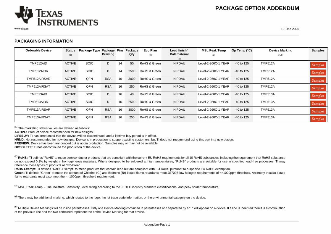
PACKAGE OPTION ADDENDUM
www.ti.com 10-Dec-2020
Addendum-Page 1
PACKAGING INFORMATION
Orderable Device Status(1)
Package Type PackageDrawing
Pins PackageQty
Eco Plan(2)
Lead finish/Ball material
(6)
MSL Peak Temp(3)
Op Temp (°C) Device Marking(4/5)
Samples
TMP512AID ACTIVE SOIC D 14 50 RoHS & Green NIPDAU Level-2-260C-1 YEAR -40 to 125 TMP512A
TMP512AIDR ACTIVE SOIC D 14 2500 RoHS & Green NIPDAU Level-2-260C-1 YEAR -40 to 125 TMP512A
TMP512AIRSAR ACTIVE QFN RSA 16 3000 RoHS & Green NIPDAU Level-2-260C-1 YEAR -40 to 125 TMP512A
TMP512AIRSAT ACTIVE QFN RSA 16 250 RoHS & Green NIPDAU Level-2-260C-1 YEAR -40 to 125 TMP512A
TMP513AID ACTIVE SOIC D 16 40 RoHS & Green NIPDAU Level-2-260C-1 YEAR -40 to 125 TMP513A
TMP513AIDR ACTIVE SOIC D 16 2500 RoHS & Green NIPDAU Level-2-260C-1 YEAR -40 to 125 TMP513A
TMP513AIRSAR ACTIVE QFN RSA 16 3000 RoHS & Green NIPDAU Level-2-260C-1 YEAR -40 to 125 TMP513A
TMP513AIRSAT ACTIVE QFN RSA 16 250 RoHS & Green NIPDAU Level-2-260C-1 YEAR -40 to 125 TMP513A
(1) The marketing status values are defined as follows:ACTIVE: Product device recommended for new designs.LIFEBUY: TI has announced that the device will be discontinued, and a lifetime-buy period is in effect.NRND: Not recommended for new designs. Device is in production to support existing customers, but TI does not recommend using this part in a new design.PREVIEW: Device has been announced but is not in production. Samples may or may not be available.OBSOLETE: TI has discontinued the production of the device.
(2) RoHS: TI defines "RoHS" to mean semiconductor products that are compliant with the current EU RoHS requirements for all 10 RoHS substances, including the requirement that RoHS substancedo not exceed 0.1% by weight in homogeneous materials. Where designed to be soldered at high temperatures, "RoHS" products are suitable for use in specified lead-free processes. TI mayreference these types of products as "Pb-Free".RoHS Exempt: TI defines "RoHS Exempt" to mean products that contain lead but are compliant with EU RoHS pursuant to a specific EU RoHS exemption.Green: TI defines "Green" to mean the content of Chlorine (Cl) and Bromine (Br) based flame retardants meet JS709B low halogen requirements of <=1000ppm threshold. Antimony trioxide basedflame retardants must also meet the <=1000ppm threshold requirement.
(3) MSL, Peak Temp. - The Moisture Sensitivity Level rating according to the JEDEC industry standard classifications, and peak solder temperature.
(4) There may be additional marking, which relates to the logo, the lot trace code information, or the environmental category on the device.
(5) Multiple Device Markings will be inside parentheses. Only one Device Marking contained in parentheses and separated by a "~" will appear on a device. If a line is indented then it is a continuationof the previous line and the two combined represent the entire Device Marking for that device.
PACKAGE OPTION ADDENDUM
www.ti.com 10-Dec-2020
Addendum-Page 2
(6) Lead finish/Ball material - Orderable Devices may have multiple material finish options. Finish options are separated by a vertical ruled line. Lead finish/Ball material values may wrap to twolines if the finish value exceeds the maximum column width.
Important Information and Disclaimer:The information provided on this page represents TI's knowledge and belief as of the date that it is provided. TI bases its knowledge and belief on informationprovided by third parties, and makes no representation or warranty as to the accuracy of such information. Efforts are underway to better integrate information from third parties. TI has taken andcontinues to take reasonable steps to provide representative and accurate information but may not have conducted destructive testing or chemical analysis on incoming materials and chemicals.TI and TI suppliers consider certain information to be proprietary, and thus CAS numbers and other limited information may not be available for release.
In no event shall TI's liability arising out of such information exceed the total purchase price of the TI part(s) at issue in this document sold by TI to Customer on an annual basis.
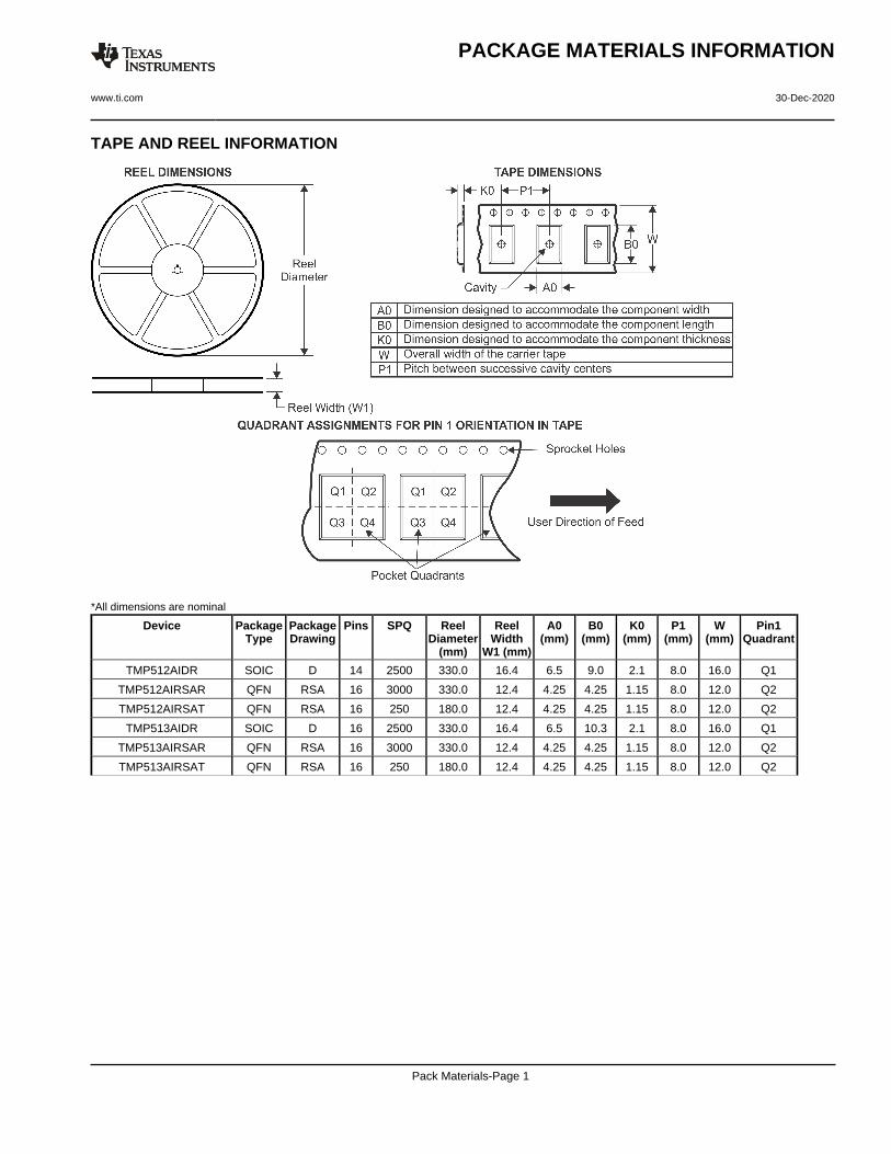
TAPE AND REEL INFORMATION
*All dimensions are nominal
Device PackageType
PackageDrawing
Pins SPQ ReelDiameter
(mm)
ReelWidth
W1 (mm)
A0(mm)
B0(mm)
K0(mm)
P1(mm)
W(mm)
Pin1Quadrant
TMP512AIDR SOIC D 14 2500 330.0 16.4 6.5 9.0 2.1 8.0 16.0 Q1
TMP512AIRSAR QFN RSA 16 3000 330.0 12.4 4.25 4.25 1.15 8.0 12.0 Q2
TMP512AIRSAT QFN RSA 16 250 180.0 12.4 4.25 4.25 1.15 8.0 12.0 Q2
TMP513AIDR SOIC D 16 2500 330.0 16.4 6.5 10.3 2.1 8.0 16.0 Q1
TMP513AIRSAR QFN RSA 16 3000 330.0 12.4 4.25 4.25 1.15 8.0 12.0 Q2
TMP513AIRSAT QFN RSA 16 250 180.0 12.4 4.25 4.25 1.15 8.0 12.0 Q2
PACKAGE MATERIALS INFORMATION
www.ti.com 30-Dec-2020
Pack Materials-Page 1
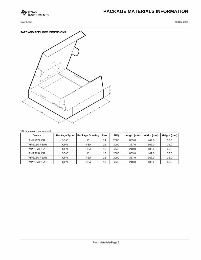
*All dimensions are nominal
Device Package Type Package Drawing Pins SPQ Length (mm) Width (mm) Height (mm)
TMP512AIDR SOIC D 14 2500 853.0 449.0 35.0
TMP512AIRSAR QFN RSA 16 3000 367.0 367.0 35.0
TMP512AIRSAT QFN RSA 16 250 210.0 185.0 35.0
TMP513AIDR SOIC D 16 2500 853.0 449.0 35.0
TMP513AIRSAR QFN RSA 16 3000 367.0 367.0 35.0
TMP513AIRSAT QFN RSA 16 250 210.0 185.0 35.0
PACKAGE MATERIALS INFORMATION
www.ti.com 30-Dec-2020
Pack Materials-Page 2
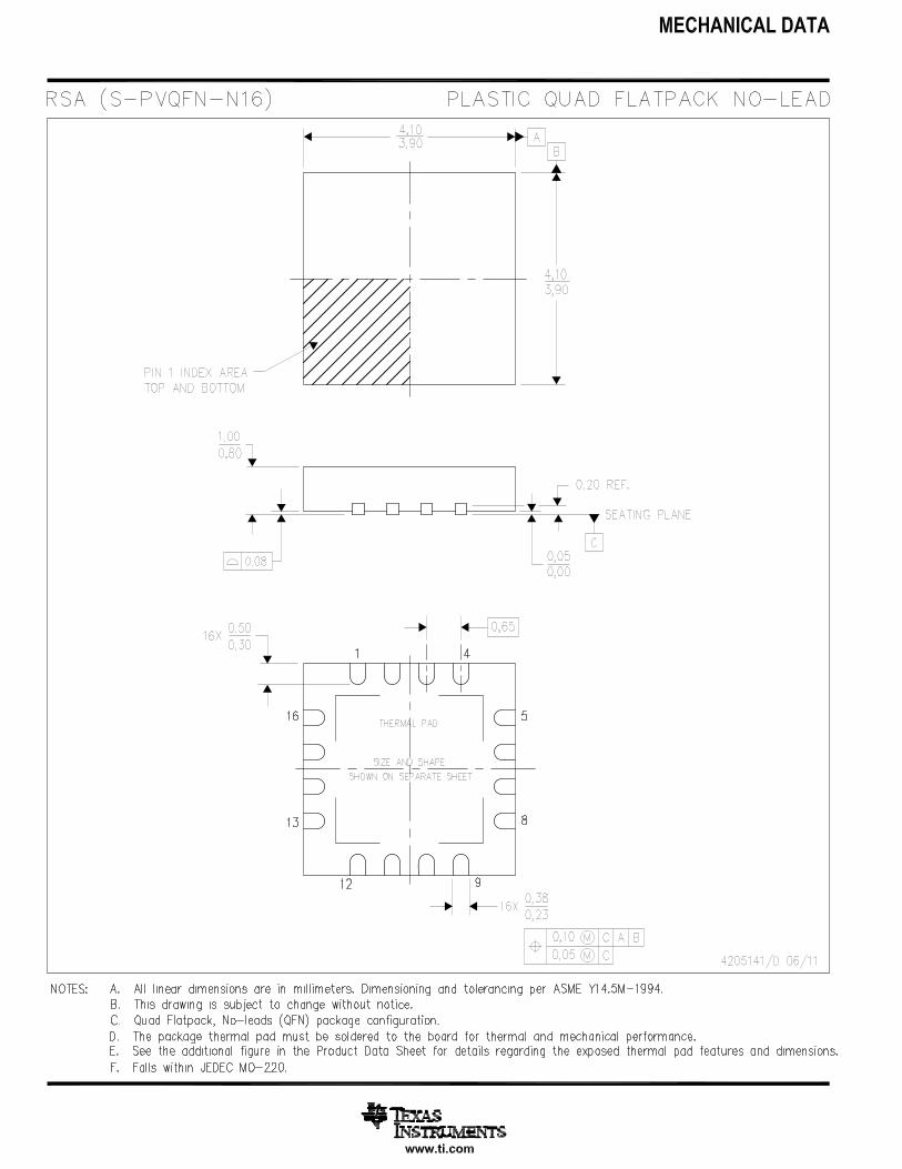
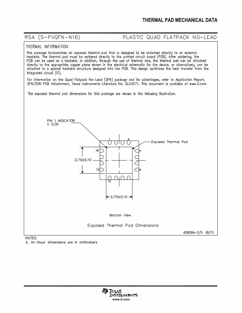
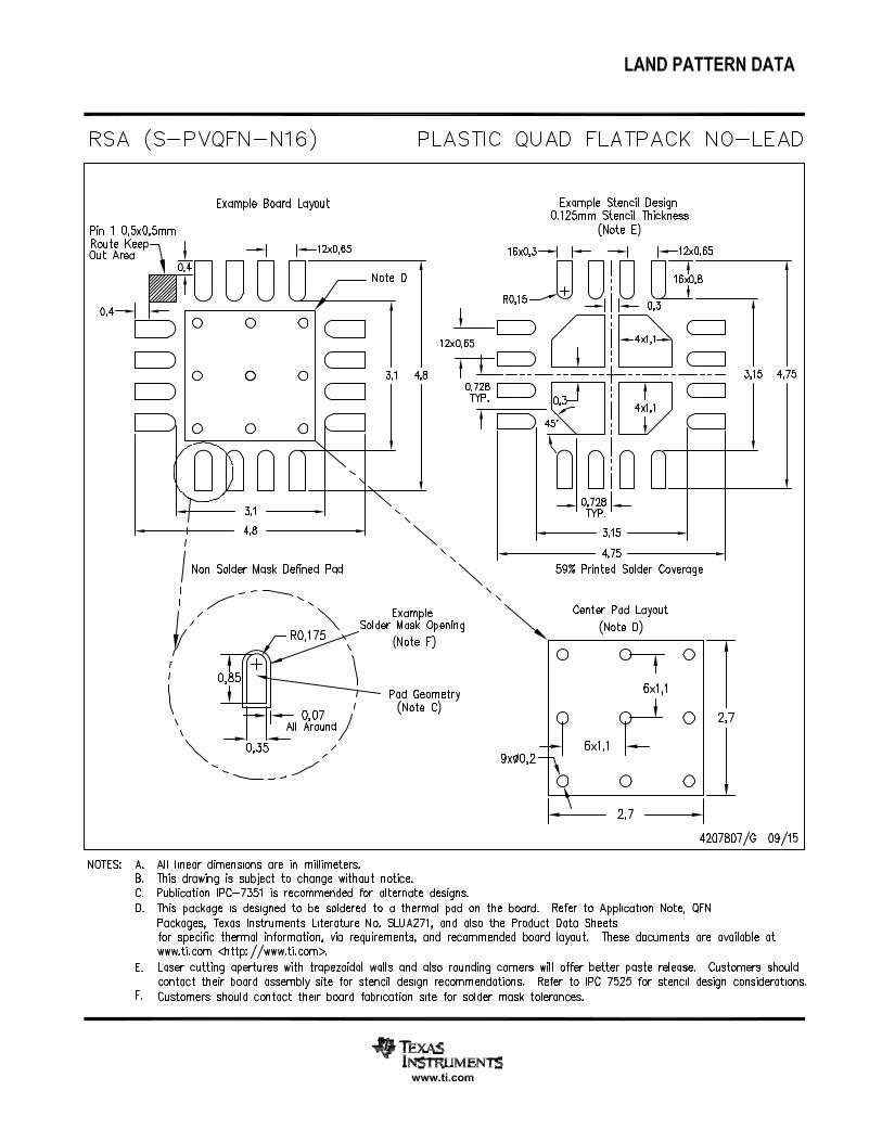

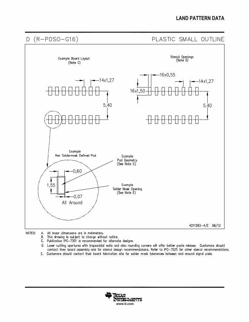

IMPORTANT NOTICE AND DISCLAIMER
TI PROVIDES TECHNICAL AND RELIABILITY DATA (INCLUDING DATASHEETS), DESIGN RESOURCES (INCLUDING REFERENCE DESIGNS), APPLICATION OR OTHER DESIGN ADVICE, WEB TOOLS, SAFETY INFORMATION, AND OTHER RESOURCES “AS IS” AND WITH ALL FAULTS, AND DISCLAIMS ALL WARRANTIES, EXPRESS AND IMPLIED, INCLUDING WITHOUT LIMITATION ANY IMPLIED WARRANTIES OF MERCHANTABILITY, FITNESS FOR A PARTICULAR PURPOSE OR NON-INFRINGEMENT OF THIRD PARTY INTELLECTUAL PROPERTY RIGHTS.These resources are intended for skilled developers designing with TI products. You are solely responsible for (1) selecting the appropriate TI products for your application, (2) designing, validating and testing your application, and (3) ensuring your application meets applicable standards, and any other safety, security, or other requirements. These resources are subject to change without notice. TI grants you permission to use these resources only for development of an application that uses the TI products described in the resource. Other reproduction and display of these resources is prohibited. No license is granted to any other TI intellectual property right or to any third party intellectual property right. TI disclaims responsibility for, and you will fully indemnify TI and its representatives against, any claims, damages, costs, losses, and liabilities arising out of your use of these resources.TI’s products are provided subject to TI’s Terms of Sale (www.ti.com/legal/termsofsale.html) or other applicable terms available either on ti.com or provided in conjunction with such TI products. TI’s provision of these resources does not expand or otherwise alter TI’s applicable warranties or warranty disclaimers for TI products.
Mailing Address: Texas Instruments, Post Office Box 655303, Dallas, Texas 75265Copyright © 2020, Texas Instruments Incorporated