temperature sensor hub and fan controller · temperature sensor hub and fan controller ... monitors...
TRANSCRIPT

Temperature Sensor Hub and Fan Controller Data Sheet ADT7470
Rev. E Document Feedback Information furnished by Analog Devices is believed to be accurate and reliable. However, no responsibility is assumed by Analog Devices for its use, nor for any infringements of patents or other rights of third parties that may result from its use. Specifications subject to change without notice. No license is granted by implication or otherwise under any patent or patent rights of Analog Devices. Trademarks and registered trademarks are the property of their respective owners.
One Technology Way, P.O. Box 9106, Norwood, MA 02062-9106, U.S.A. Tel: 781.329.4700 ©2004–2013 Analog Devices, Inc. All rights reserved. Technical Support www.analog.com
FEATURES Monitors up to 10 remote temperature sensors Monitors and controls speed of up to 4 fans independently PWM outputs drive each fan under software control FULL_SPEED input allows fans to be blasted to maximum
speed by external hardware SMBALERT interrupt signals failures to system controller Three-state ADDR pin allows up to 3 devices on a single bus Temperature decoder interprets TMP05 temperature sensors
and communicates values over I2C bus Limit comparison of all monitored values Supports fast I2C standard (400 kHz max) Meets SMBus 2.0 electrical specifications
(fully SMBus 1.1-compliant)
APPLICATIONS Servers Networking and telecommunications equipment Desktops
GENERAL DESCRIPTION The ADT74701 controller is a multichannel temperature sensor and PWM fan controller and fan speed monitor for systems requiring active cooling. It is designed to interface directly to an I2C® bus. The ADT7470 can monitor up to 10 daisy-chained TMP05 temperature sensors. It can also monitor and control the speed of four fans, in automatic or in manual control loops.
A FULL_SPEED input is provided to allow the fans to be blasted to maximum speed, via external hardware control, under extreme thermal conditions or on system startup. An SMBALERT interrupt communicates error conditions such as fan under speed and over temperature measurements to the system service processor. Individual error conditions can then be read from status registers over the I2C bus.
FUNCTIONAL BLOCK DIAGRAM
FULL_SPEED
PWM1
PWM2
PWM3
PWM4
TACH1TACH2TACH3TACH4
TMP_START
TMP_IN
ADDR SDA SCL SMBALERT
ADDRESSPOINTER
REGISTER
PWMCONFIG
REGISTERS
INTERRUPTMASKING
INTERRUPTSTATUS
REGISTERS
LIMITCOMPARATORS
VALUE ANDLIMIT
REGISTERS
SERIAL BUSINTERFACE
SMBusADDRESS
SELECTION
AUTOMATICFAN SPEEDCONTROL
PWMREGISTERS
ANDCONTROLLERS
FAN SPEEDCOUNTERS
TEMPERATUREDECODER
0468
4-0-
001
ADT7470
Figure 1.
1 Protected by Patent Numbers US6,169,442, US6,097,239, US5,982,221, US5,867,012. Other patents pending.
ADT7470 Data Sheet
Rev. E | Page 2 of 40
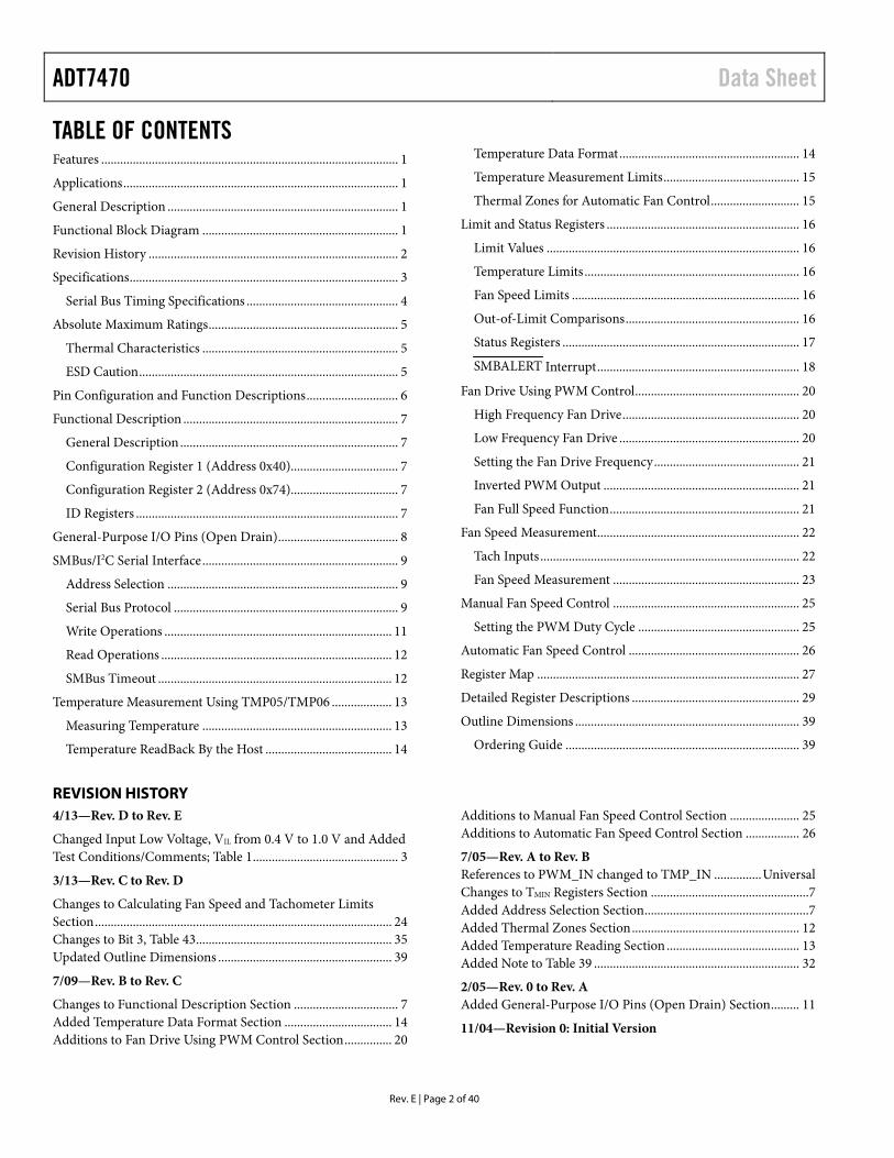
TABLE OF CONTENTS Features .............................................................................................. 1 Applications ....................................................................................... 1 General Description ......................................................................... 1 Functional Block Diagram .............................................................. 1 Revision History ............................................................................... 2 Specifications ..................................................................................... 3
Serial Bus Timing Specifications ................................................ 4 Absolute Maximum Ratings ............................................................ 5
Thermal Characteristics .............................................................. 5 ESD Caution .................................................................................. 5
Pin Configuration and Function Descriptions ............................. 6 Functional Description .................................................................... 7
General Description ..................................................................... 7 Configuration Register 1 (Address 0x40).................................. 7 Configuration Register 2 (Address 0x74).................................. 7 ID Registers ................................................................................... 7
General-Purpose I/O Pins (Open Drain) ...................................... 8 SMBus/I2C Serial Interface .............................................................. 9
Address Selection ......................................................................... 9 Serial Bus Protocol ....................................................................... 9 Write Operations ........................................................................ 11 Read Operations ......................................................................... 12 SMBus Timeout .......................................................................... 12
Temperature Measurement Using TMP05/TMP06 ................... 13 Measuring Temperature ............................................................ 13 Temperature ReadBack By the Host ........................................ 14
Temperature Data Format ......................................................... 14 Temperature Measurement Limits ........................................... 15 Thermal Zones for Automatic Fan Control ............................ 15
Limit and Status Registers ............................................................. 16 Limit Values ................................................................................ 16 Temperature Limits .................................................................... 16 Fan Speed Limits ........................................................................ 16 Out-of-Limit Comparisons ....................................................... 16 Status Registers ........................................................................... 17 SMBALERT Interrupt ................................................................ 18
Fan Drive Using PWM Control .................................................... 20 High Frequency Fan Drive ........................................................ 20 Low Frequency Fan Drive ......................................................... 20 Setting the Fan Drive Frequency .............................................. 21 Inverted PWM Output .............................................................. 21 Fan Full Speed Function ............................................................ 21
Fan Speed Measurement ................................................................ 22 Tach Inputs .................................................................................. 22 Fan Speed Measurement ........................................................... 23
Manual Fan Speed Control ........................................................... 25 Setting the PWM Duty Cycle ................................................... 25
Automatic Fan Speed Control ...................................................... 26 Register Map ................................................................................... 27 Detailed Register Descriptions ..................................................... 29 Outline Dimensions ....................................................................... 39
Ordering Guide .......................................................................... 39
REVISION HISTORY 4/13—Rev. D to Rev. E
Changed Input Low Voltage, VIL from 0.4 V to 1.0 V and Added Test Conditions/Comments; Table 1 .............................................. 3
3/13—Rev. C to Rev. D
Changes to Calculating Fan Speed and Tachometer Limits Section .............................................................................................. 24 Changes to Bit 3, Table 43.............................................................. 35 Updated Outline Dimensions ....................................................... 39
7/09—Rev. B to Rev. C
Changes to Functional Description Section ................................. 7 Added Temperature Data Format Section .................................. 14 Additions to Fan Drive Using PWM Control Section ............... 20
Additions to Manual Fan Speed Control Section ...................... 25 Additions to Automatic Fan Speed Control Section ................. 26
7/05—Rev. A to Rev. B References to PWM_IN changed to TMP_IN ............... Universal Changes to TMIN Registers Section .................................................. 7 Added Address Selection Section .................................................... 7 Added Thermal Zones Section ..................................................... 12 Added Temperature Reading Section .......................................... 13 Added Note to Table 39 ................................................................. 32
2/05—Rev. 0 to Rev. A Added General-Purpose I/O Pins (Open Drain) Section ......... 11
11/04—Revision 0: Initial Version

Data Sheet ADT7470
Rev. E | Page 3 of 40
SPECIFICATIONS TA = −40oC to +125oC, VCC = 3.0 V to 5.5 V, unless otherwise noted.
Table 1. Parameter1, 2, 3, 4, 5 Min Typ Max Unit Test Conditions/Comments POWER SUPPLY1
Supply Voltage 3.0 3.3 5.5 V Supply Current, ICC 0.5 0.8 mA Standby Current, ICC 4 µA
FAN RPM-TO-DIGITAL CONVERTER Accuracy ±12 % Full-Scale Count 65,535 Nominal Input RPM 109 RPM Fan count = 0xBFFF
329 RPM Fan count = 0x3FFF 5,000 RPM Fan count = 0x0438 10,000 RPM Fan count = 0x021C OPEN-DRAIN DIGITAL OUTPUTS, PWM1 to PWM4, SMBALERT
Output Low Voltage, VOL 0.4 V IOUT = –8.0 mA, VCC = +3.3 V High Level Output Current, IOH 0.1 1 µA VOUT = VCC
OPEN-DRAIN SERIAL DATA BUS OUTPUT (SDA) Output Low Voltage, VOL 0.4 V IOUT = –4.0 mA, VCC = +3.3 V High Level Output Current, IOH 0.1 1 µA VOUT = VCC
SMBus DIGITAL INPUTS (SCL, SDA) Input High Voltage, VIH 2.4 V Input Low Voltage, VIL 1.0 V VCC = 3.3 V Hysteresis 500 mV
DIGITAL INPUT LOGIC LEVELS (TACH INPUTS, FULL_SPEED, GPIO)
Input High Voltage, VIH 2.4 V Input Low Voltage, VIL 0.8 V Hysteresis 50 mV p-p
DIGITAL INPUT LOGIC LEVELS (TMP_IN) Input High Voltage, VIH VDD – 0.3 V Input Low Voltage, VIL 0.4 V
DIGITAL INPUT CURRENT Input High Current, IIH –5 µA VIN = VCC Input Low Current, IIL 5 µA VIN = 0 Input Capacitance, CIN 5 pF
1 VDD should never be floated in the presence of SCL/SDA activity. Charge injection can be sufficient to induce approximately 0.6 V on VDD. 2 All voltages are measured with respect to GND, unless otherwise specified. 3 Typical values are at %A = 25°C and represent the most likely parametric norm. 4 Logic inputs accept input high voltages up to 5 V even when the device is operating at supply voltages below 5 V. 5 Timing specifications are tested at logic levels of VIL = 0.8 V for a falling edge and VIH = 2.0 V for a rising edge.

ADT7470 Data Sheet
Rev. E | Page 4 of 40
SERIAL BUS TIMING SPECIFICATIONS
Table 2. Parameter1, 2, 3, 4, 5 Min Typ Max Unit Test Conditions/Comments SERIAL BUS TIMING
Clock Frequency, fSCLK 400 kHz See Figure 2 Glitch Immunity, tSW 50 ns See Figure 2 Bus Free Time, tBUF 1.3 μs See Figure 2 Start Setup Time, tSU;STA 600 ns See Figure 2 Start Hold Time, tHD;STA 600 ns See Figure 2 SCL Low Time, tLOW 1.3 μs See Figure 2 SCL High Time, tHIGH 0.6 μs See Figure 2 SCL, SDA Rise Time, tr 300 ns See Figure 2 SCL, SDA Fall Time, tf 300 ns See Figure 2 Data Setup Time, tSU;DAT 100 ns See Figure 2 Detect Clock Low Timeout, tTIMEOUT 25 28 31 ms Can be optionally disabled,
via Configuration Register 1 (see Table 6)
1 VDD should never be floated in the presence of SCL/SDA activity. Charge injection can be sufficient to induce approximately 0.6 V on VDD. 2 All voltages are measured with respect to GND, unless otherwise specified. 3 Typical values are at %A = 25°C and represent the most likely parametric norm. 4 Logic inputs accept input high voltages up to 5 V even when the device is operating at supply voltages below 5 V. 5 Timing specifications are tested at logic levels of VIL = 0.8 V for a falling edge and VIH = 2.0 V for a rising edge.
0468
4-0-
002
SCL
SDA
P StBUF
tHD;STA tHD;DAT
tHIGHtSU;DAT
tHD;STA
tSU;STA tSU;STO
tLOW
tR tF
S P Figure 2. Serial Bus Timing Diagram
Data Sheet ADT7470
Rev. E | Page 5 of 40
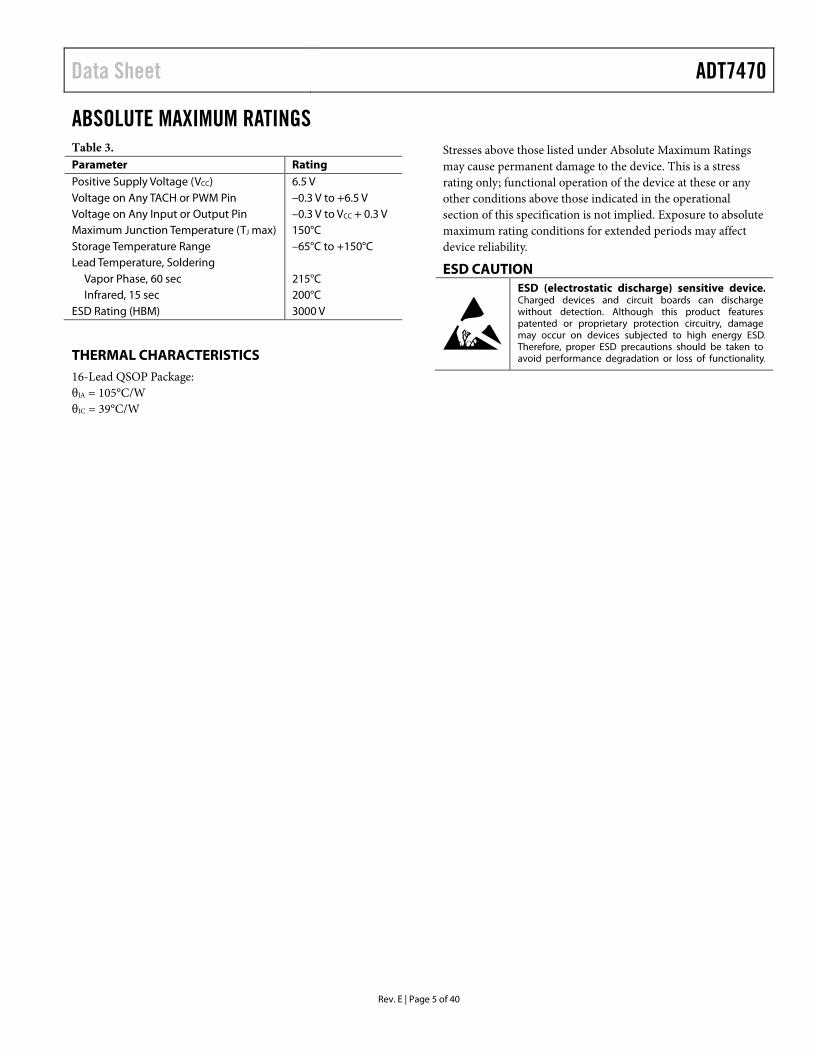
ABSOLUTE MAXIMUM RATINGS Table 3. Parameter Rating Positive Supply Voltage (VCC) 6.5 V Voltage on Any TACH or PWM Pin –0.3 V to +6.5 V Voltage on Any Input or Output Pin –0.3 V to VCC + 0.3 V Maximum Junction Temperature (TJ max) 150°C Storage Temperature Range –65°C to +150°C Lead Temperature, Soldering
Vapor Phase, 60 sec 215°C Infrared, 15 sec 200°C
ESD Rating (HBM) 3000 V
THERMAL CHARACTERISTICS 16-Lead QSOP Package: θJA = 105°C/W θJC = 39°C/W
Stresses above those listed under Absolute Maximum Ratings may cause permanent damage to the device. This is a stress rating only; functional operation of the device at these or any other conditions above those indicated in the operational section of this specification is not implied. Exposure to absolute maximum rating conditions for extended periods may affect device reliability.
ESD CAUTION
ADT7470 Data Sheet
Rev. E | Page 6 of 40
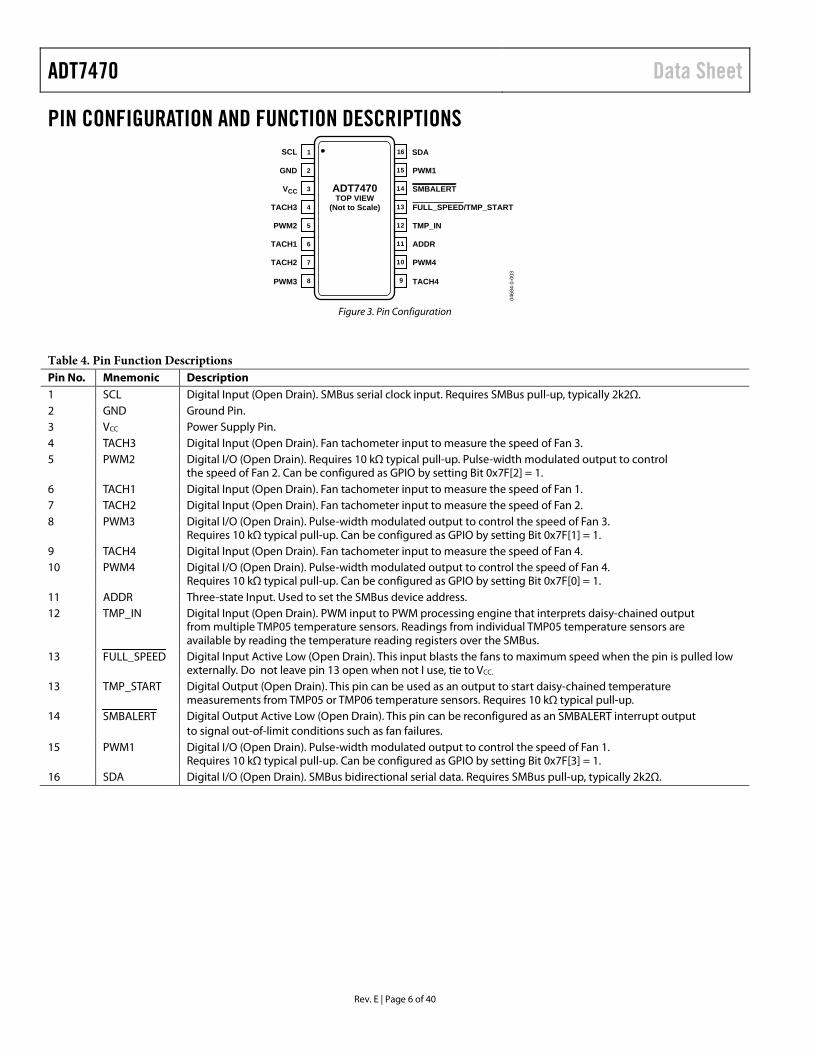
PIN CONFIGURATION AND FUNCTION DESCRIPTIONS
0468
4-0-
003
1
2
3
4
5
6
7
8
16
15
14
13
12
11
10
9
GND
VCC
TACH3
TACH2
TACH1
PWM2
SCL
PWM1
SMBALERT
FULL_SPEED/TMP_START
PWM4
PWM3 TACH4
ADDR
TMP_IN
SDA
ADT7470TOP VIEW
(Not to Scale)
Figure 3. Pin Configuration
Table 4. Pin Function Descriptions Pin No. Mnemonic Description 1 SCL Digital Input (Open Drain). SMBus serial clock input. Requires SMBus pull-up, typically 2k2Ω. 2 GND Ground Pin. 3 VCC Power Supply Pin. 4 TACH3 Digital Input (Open Drain). Fan tachometer input to measure the speed of Fan 3. 5 PWM2 Digital I/O (Open Drain). Requires 10 kΩ typical pull-up. Pulse-width modulated output to control
the speed of Fan 2. Can be configured as GPIO by setting Bit 0x7F[2] = 1. 6 TACH1 Digital Input (Open Drain). Fan tachometer input to measure the speed of Fan 1. 7 TACH2 Digital Input (Open Drain). Fan tachometer input to measure the speed of Fan 2. 8 PWM3 Digital I/O (Open Drain). Pulse-width modulated output to control the speed of Fan 3.
Requires 10 kΩ typical pull-up. Can be configured as GPIO by setting Bit 0x7F[1] = 1. 9 TACH4 Digital Input (Open Drain). Fan tachometer input to measure the speed of Fan 4. 10 PWM4 Digital I/O (Open Drain). Pulse-width modulated output to control the speed of Fan 4.
Requires 10 kΩ typical pull-up. Can be configured as GPIO by setting Bit 0x7F[0] = 1. 11 ADDR Three-state Input. Used to set the SMBus device address. 12 TMP_IN Digital Input (Open Drain). PWM input to PWM processing engine that interprets daisy-chained output
from multiple TMP05 temperature sensors. Readings from individual TMP05 temperature sensors are available by reading the temperature reading registers over the SMBus.
13 FULL_SPEED Digital Input Active Low (Open Drain). This input blasts the fans to maximum speed when the pin is pulled low externally. Do not leave pin 13 open when not I use, tie to VCC.
13 TMP_START Digital Output (Open Drain). This pin can be used as an output to start daisy-chained temperature measurements from TMP05 or TMP06 temperature sensors. Requires 10 kΩ typical pull-up.
14 SMBALERT Digital Output Active Low (Open Drain). This pin can be reconfigured as an SMBALERT interrupt output to signal out-of-limit conditions such as fan failures.
15 PWM1 Digital I/O (Open Drain). Pulse-width modulated output to control the speed of Fan 1. Requires 10 kΩ typical pull-up. Can be configured as GPIO by setting Bit 0x7F[3] = 1.
16 SDA Digital I/O (Open Drain). SMBus bidirectional serial data. Requires SMBus pull-up, typically 2k2Ω.
Data Sheet ADT7470
Rev. E | Page 7 of 40
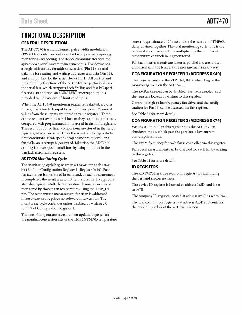
FUNCTIONAL DESCRIPTION GENERAL DESCRIPTION The ADT7470 is a multichannel, pulse-width modulation (PWM) fan controller and monitor for any system requiring monitoring and cooling. The device communicates with the system via a serial system management bus. The device has a single address line for address selection (Pin 11), a serial data line for reading and writing addresses and data (Pin 16), and an input line for the serial clock (Pin 1). All control and programming functions of the ADT7470 are performed over the serial bus, which supports both SMBus and fast I2C speci-fications. In addition, an SMBALERT interrupt output is provided to indicate out-of-limit conditions.
When the ADT7470 monitoring sequence is started, it cycles through each fan tach input to measure fan speed. Measured values from these inputs are stored in value registers. These can be read out over the serial bus, or they can be automatically compared with programmed limits stored in the limit registers. The results of out-of-limit comparisons are stored in the status registers, which can be read over the serial bus to flag out-of-limit conditions. If fan speeds drop below preset levels or a fan stalls, an interrupt is generated. Likewise, the ADT7470 can flag fan over speed conditions by using limits set in the fan tach maximum registers.
ADT7470 Monitoring Cycle
The monitoring cycle begins when a 1 is written to the start bit (Bit 0) of Configuration Register 1 (Register 0x40). Each fan tach input is monitored in turn, and, as each measurement is completed, the result is automatically stored in the appropri-ate value register. Multiple temperature channels can also be monitored by clocking in temperatures using the TMP_IN pin. The temperature measurement function is addressed in hardware and requires no software intervention. The monitoring cycle continues unless disabled by writing a 0 to Bit 7 of Configuration Register 1.
The rate of temperature measurement updates depends on the nominal conversion rate of the TMP05/TMP06 temperature
sensor (approximately 120 ms) and on the number of TMP05s daisy-chained together. The total monitoring cycle time is the temperature conversion time multiplied by the number of temperature channels being monitored.
Fan tach measurements are taken in parallel and are not syn-chronized with the temperature measurements in any way
CONFIGURATION REGISTER 1 (ADDRESS 0X40) This register contains the STRT bit, Bit 0, which begins the monitoring cycle on the ADT7470.
The SMBus timeout can be disabled , fast tach enabled, and the registers locked, by writing to this register.
Control of high or low frequency fan drive, and the config-uration for Pin 13, can be accessed via this register.
See Table 31 for more details.
CONFIGURATION REGISTER 2 (ADDRESS 0X74) Writing a 1 to Bit 0 in this register puts the ADT7470 in shutdown mode, which puts the part into a low current consumption mode.
The PWM frequency for each fan is controlled via this register.
Fan speed measurement can be disabled for each fan by writing to this register.
See Table 44 for more details.
ID REGISTERS The ADT7470 has three read-only registers for identifying the part and silicon revision.
The device ID register is located at address 0x3D, and is set to 0x70.
The company ID register, located at address 0x3E, is set to 0x41.
The revision number register is at address 0x3F, and contains the revision number of the ADT7470 silicon.

ADT7470 Data Sheet
Rev. E | Page 8 of 40
GENERAL-PURPOSE I/O PINS (OPEN DRAIN) The ADT7470 has four pins that can be configured as either general-purpose logic pins or as PWM outputs. Each GPIO pin has a corresponding enable, direction, polarity and status bit.
Pin Function Register Address and Bit GPIO1 Enable 0x7F [3] Direction 0x80 [7] Polarity 0x80 [6] Status 0x81 [4] GPIO2 Enable 0x7F [2] Direction 0x80 [5] Polarity 0x80 [4] Status 0x81 [5] GPIO3 Enable 0x7F [1] Direction 0x80 [3] Polarity 0x80 [2] Status 0x81 [6] GPIO4 Enable 0x7F [0] Direction 0x80 [1] Polarity 0x80 [0] Status 0x81 [7]
To enable the PWM output on the ADT7470 as GPIOs, the enable bits in Register 0x7F must be set to 1.
Setting a direction bit to 1 in the GPIO configuration register makes the corresponding GPIO pin an output. Clearing the direction bit to 0 makes it an input.
Setting a polarity bit to 1 makes the corresponding GPIO pin active high. Clearing the polarity bit to 0 makes it active low.
When a GPIO pin is configured as an input, the corresponding bit in the GPIO status register is read-only and is set when the input is asserted. When a GPIO pin is configured as an output, the corresponding bit in one of the GPIO status registers becomes read/write. Setting this bit asserts the GPIO output. Note that whether a GPIO pin is configured as an input or as an output, asserted can be high or low, depending on the setting of the polarity bit.
Data Sheet ADT7470
Rev. E | Page 9 of 40
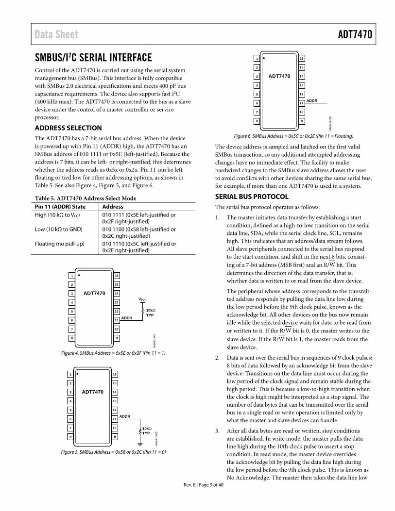
SMBUS/I2C SERIAL INTERFACE Control of the ADT7470 is carried out using the serial system management bus (SMBus). This interface is fully compatible with SMBus 2.0 electrical specifications and meets 400 pF bus capacitance requirements. The device also supports fast I2C (400 kHz max). The ADT7470 is connected to the bus as a slave device under the control of a master controller or service processor.
ADDRESS SELECTION The ADT7470 has a 7-bit serial bus address. When the device is powered up with Pin 11 (ADDR) high, the ADT7470 has an SMBus address of 010 1111 or 0x5E (left-justified). Because the address is 7 bits, it can be left- or right-justified; this determines whether the address reads as 0x5x or 0x2x. Pin 11 can be left floating or tied low for other addressing options, as shown in Table 5. See also Figure 4, Figure 5, and Figure 6.
Table 5. ADT7470 Address Select Mode Pin 11 (ADDR) State Address High (10 kΩ to VCC) 010 1111 (0x5E left-justified or
0x2F right-justified) Low (10 kΩ to GND) 010 1100 (0x58 left-justified or
0x2C right-justified) Floating (no pull-up) 010 1110 (0x5C left-justified or
0x2E right-justified)
VCC
10kΩTYP
ADDR
0468
4-0-
004
1
2
3
4
5
6
7
8
16
15
14
13
12
11
10
9
ADT7470
Figure 4. SMBus Address = 0x5E or 0x2F (Pin 11 = 1)
ADDR
10kΩTYP
0468
4-0-
005
1
2
3
4
5
6
7
8
16
15
14
13
12
11
10
9
ADT7470
Figure 5. SMBus Address = 0x58 or 0x2C (Pin 11 = 0)
ADDR
0468
4-0-
006
1
2
3
4
5
6
7
8
16
15
14
13
12
11
10
9
ADT7470
Figure 6. SMBus Address = 0x5C or 0x2E (Pin 11 = Floating)
The device address is sampled and latched on the first valid SMBus transaction, so any additional attempted addressing changes have no immediate effect. The facility to make hardwired changes to the SMBus slave address allows the user to avoid conflicts with other devices sharing the same serial bus, for example, if more than one ADT7470 is used in a system.
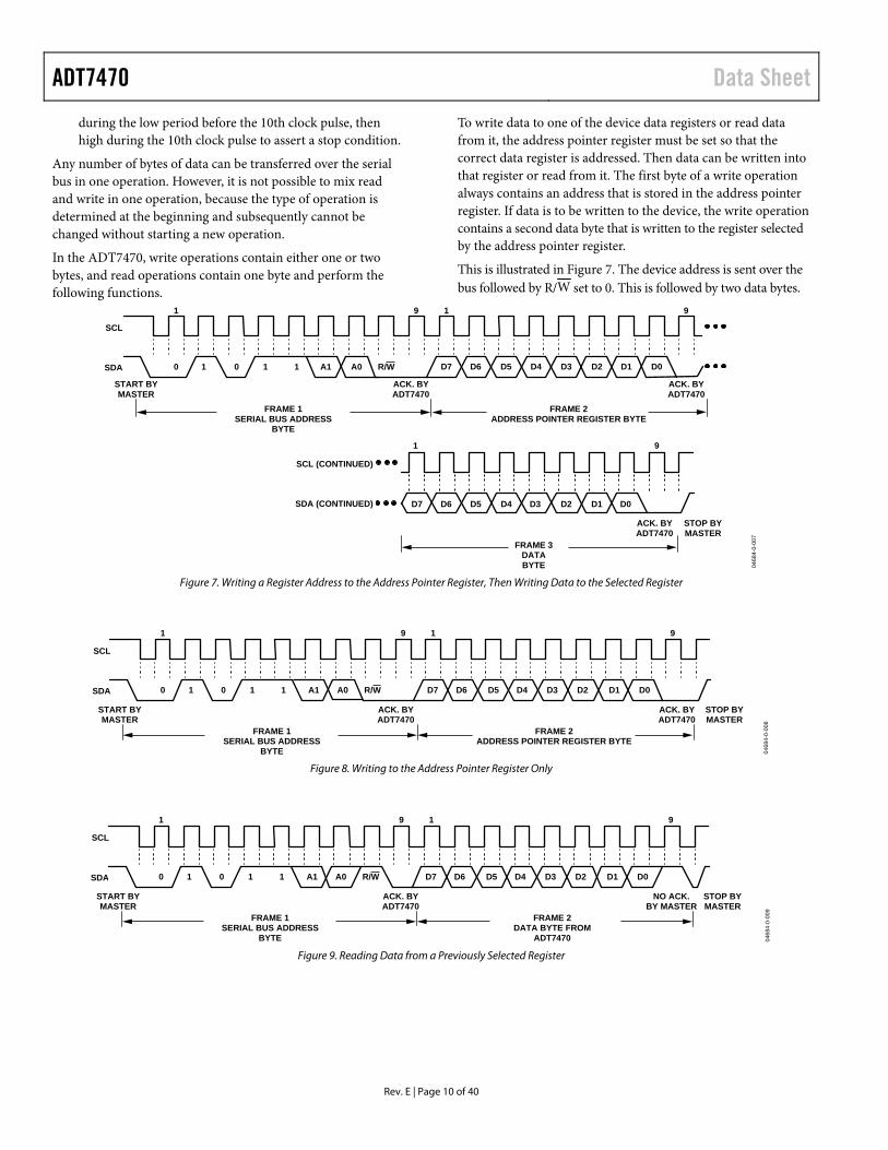
SERIAL BUS PROTOCOL The serial bus protocol operates as follows:
1. The master initiates data transfer by establishing a start condition, defined as a high-to-low transition on the serial data line, SDA, while the serial clock line, SCL, remains high. This indicates that an address/data stream follows. All slave peripherals connected to the serial bus respond to the start condition, and shift in the next 8 bits, consist-ing of a 7-bit address (MSB first) and an R/W bit. This determines the direction of the data transfer, that is, whether data is written to or read from the slave device.
The peripheral whose address corresponds to the transmit-ted address responds by pulling the data line low during the low period before the 9th clock pulse, known as the acknowledge bit. All other devices on the bus now remain idle while the selected device waits for data to be read from or written to it. If the R/W bit is 0, the master writes to the slave device. If the R/W bit is 1, the master reads from the slave device.
2. Data is sent over the serial bus in sequences of 9 clock pulses: 8 bits of data followed by an acknowledge bit from the slave device. Transitions on the data line must occur during the low period of the clock signal and remain stable during the high period. This is because a low-to-high transition when the clock is high might be interpreted as a stop signal. The number of data bytes that can be transmitted over the serial bus in a single read or write operation is limited only by what the master and slave devices can handle.
3. After all data bytes are read or written, stop conditions are established. In write mode, the master pulls the data line high during the 10th clock pulse to assert a stop condition. In read mode, the master device overrides the acknowledge bit by pulling the data line high during the low period before the 9th clock pulse. This is known as No Acknowledge. The master then takes the data line low
ADT7470 Data Sheet
Rev. E | Page 10 of 40
during the low period before the 10th clock pulse, then high during the 10th clock pulse to assert a stop condition.
Any number of bytes of data can be transferred over the serial bus in one operation. However, it is not possible to mix read and write in one operation, because the type of operation is determined at the beginning and subsequently cannot be changed without starting a new operation.
In the ADT7470, write operations contain either one or two bytes, and read operations contain one byte and perform the following functions.
To write data to one of the device data registers or read data from it, the address pointer register must be set so that the correct data register is addressed. Then data can be written into that register or read from it. The first byte of a write operation always contains an address that is stored in the address pointer register. If data is to be written to the device, the write operation contains a second data byte that is written to the register selected by the address pointer register.
This is illustrated in Figure 7. The device address is sent over the bus followed by R/W set to 0. This is followed by two data bytes.
0468
4-0-
007
1
0 01 1 1 A1 A0 R/W
9 91
1
D7 D6 D5 D4 D3 D2 D1 D0
9
D7 D6 D5 D4 D3 D2 D1 D0
SCL
SDA
SCL (CONTINUED)
SDA (CONTINUED)
START BYMASTER
ACK. BYADT7470
ACK. BYADT7470
ACK. BYADT7470
STOP BYMASTER
FRAME 1SERIAL BUS ADDRESS
BYTE
FRAME 2ADDRESS POINTER REGISTER BYTE
FRAME 3DATABYTE
Figure 7. Writing a Register Address to the Address Pointer Register, Then Writing Data to the Selected Register
SCL
SDA
1
0 1 0 1 1 A1 A0
START BYMASTER
FRAME 1SERIAL BUS ADDRESS
BYTE
FRAME 2ADDRESS POINTER REGISTER BYTE
STOP BYMASTER
ACK. BYADT7470
ACK. BYADT7470
R/W D7 D6 D5 D4 D3 D2 D1 D0
9 91
0468
4-0-
008
Figure 8. Writing to the Address Pointer Register Only
0468
4-0-
009
SCL
SDA
1
0 1 0 1 1 A1 A0
START BYMASTER
FRAME 1SERIAL BUS ADDRESS
BYTE
FRAME 2DATA BYTE FROM
ADT7470
STOP BYMASTER
ACK. BYADT7470
NO ACK.BY MASTER
R/W D7 D6 D5 D4 D3 D2 D1 D0
9 91
Figure 9. Reading Data from a Previously Selected Register
Data Sheet ADT7470
Rev. E | Page 11 of 40
The first data byte is the address of the internal data register to be written to, which is stored in the address pointer register. The second data byte is the data to be written to the internal data register.
How data is read from a register depends on whether or not the address pointer register value is known.
If the ADT7470 address pointer register value is unknown or not the desired value, it is first necessary to set it to the correct value before data can be read from the desired data register. This is done by performing a write to the ADT7470 as before, but only the data byte containing the register address is sent, because data cannot be written to the register. This is shown in Figure 8.
A read operation is then performed consisting of the serial bus address, R/W bit set to 1, followed by the data byte read from the data register. This is shown in Figure 9.
If the address pointer register is known to be already at the desired address, data can be read from the corresponding data register without first writing to the address pointer register, so the operation shown in Figure 8 can be omitted.
Note the following:
• Although it is possible to read a data byte from a data register without first writing to the address pointer register if the address pointer register is already at the correct value, it is not possible to write data to a register without writing to the address pointer register. This is because the first data byte of a write is always written to the address pointer register.
• In Figure 7 to Figure 9, the serial bus address is shown as the default value 01011(A1)(A0), where A1 and A0 are set by the address select mode function previously defined.
• In addition to supporting the send byte and receive byte protocols, the ADT7470 also supports the read byte protocol. See System Management Bus Specifications Rev. 2.0 for more information.
• If it is required to perform several read or write operations in succession, the master can send a repeat start condition instead of a stop condition to begin a new operation.
WRITE OPERATIONS The SMBus specification defines several protocols for different types of read and write operations. The protocols used in the ADT7470 are discussed in the following sections. The following abbreviations are used in the diagrams:
S—Start P—Stop R—Read W—Write A—Acknowledge A—No Acknowledge
The ADT7470 uses the following SMBus write protocols.
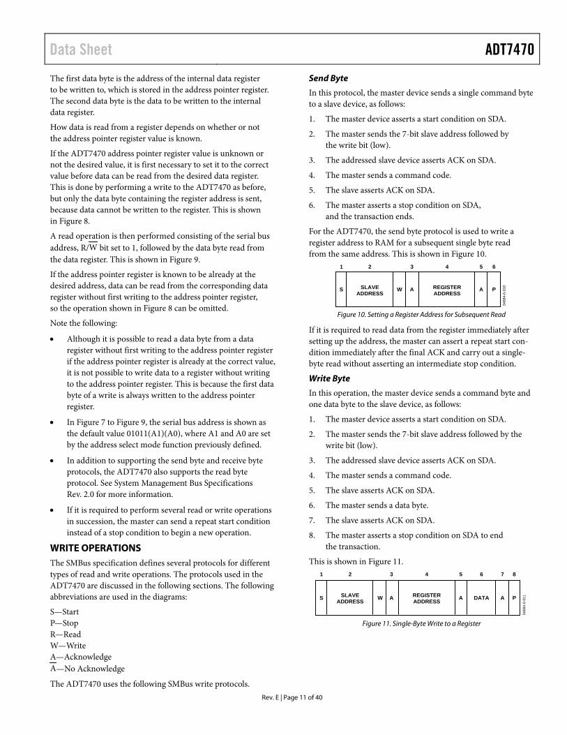
Send Byte
In this protocol, the master device sends a single command byte to a slave device, as follows:
1. The master device asserts a start condition on SDA.
2. The master sends the 7-bit slave address followed by the write bit (low).
3. The addressed slave device asserts ACK on SDA.
4. The master sends a command code.
5. The slave asserts ACK on SDA.
6. The master asserts a stop condition on SDA, and the transaction ends.
For the ADT7470, the send byte protocol is used to write a register address to RAM for a subsequent single byte read from the same address. This is shown in Figure 10.
1 2 3 4 5 6
S W A A PSLAVEADDRESS
REGISTERADDRESS
0468
4-0-
010
Figure 10. Setting a Register Address for Subsequent Read
If it is required to read data from the register immediately after setting up the address, the master can assert a repeat start con-dition immediately after the final ACK and carry out a single-byte read without asserting an intermediate stop condition.
Write Byte
In this operation, the master device sends a command byte and one data byte to the slave device, as follows:
1. The master device asserts a start condition on SDA.
2. The master sends the 7-bit slave address followed by the write bit (low).
3. The addressed slave device asserts ACK on SDA.
4. The master sends a command code.
5. The slave asserts ACK on SDA.
6. The master sends a data byte.
7. The slave asserts ACK on SDA.
8. The master asserts a stop condition on SDA to end the transaction.
This is shown in Figure 11. 1 2 3 4 5 6 7 8
S W A A A PDATASLAVEADDRESS
REGISTERADDRESS
0468
4-0-
011
Figure 11. Single-Byte Write to a Register
ADT7470 Data Sheet
Rev. E | Page 12 of 40
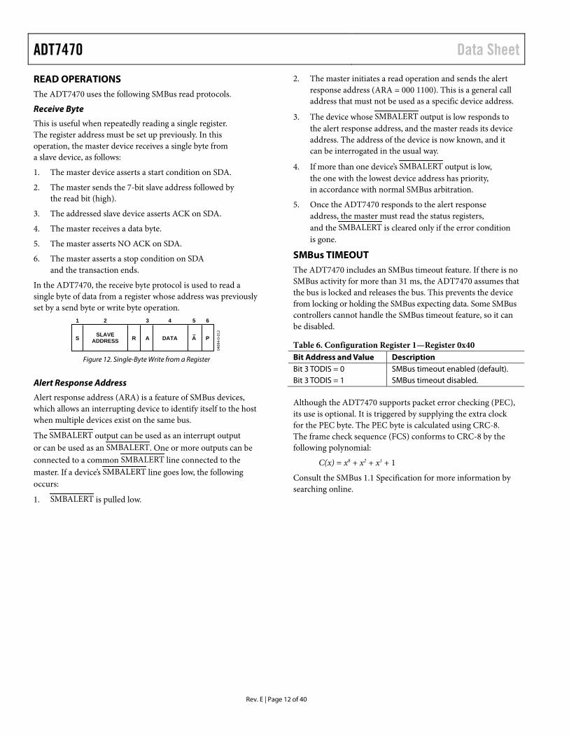
READ OPERATIONS The ADT7470 uses the following SMBus read protocols.
Receive Byte
This is useful when repeatedly reading a single register. The register address must be set up previously. In this operation, the master device receives a single byte from a slave device, as follows:
1. The master device asserts a start condition on SDA.
2. The master sends the 7-bit slave address followed by the read bit (high).
3. The addressed slave device asserts ACK on SDA.
4. The master receives a data byte.
5. The master asserts NO ACK on SDA.
6. The master asserts a stop condition on SDA and the transaction ends.
In the ADT7470, the receive byte protocol is used to read a single byte of data from a register whose address was previously set by a send byte or write byte operation.
1 2 3 4 5 6
S R A DATA A PSLAVEADDRESS
0468
4-0-
012
Figure 12. Single-Byte Write from a Register
Alert Response Address
Alert response address (ARA) is a feature of SMBus devices, which allows an interrupting device to identify itself to the host when multiple devices exist on the same bus.
The SMBALERT output can be used as an interrupt output or can be used as an SMBALERT. One or more outputs can be connected to a common SMBALERT line connected to the master. If a device’s SMBALERT line goes low, the following occurs:
1. SMBALERT is pulled low.
2. The master initiates a read operation and sends the alert response address (ARA = 000 1100). This is a general call address that must not be used as a specific device address.
3. The device whose SMBALERT output is low responds to the alert response address, and the master reads its device address. The address of the device is now known, and it can be interrogated in the usual way.
4. If more than one device’s SMBALERT output is low, the one with the lowest device address has priority, in accordance with normal SMBus arbitration.
5. Once the ADT7470 responds to the alert response address, the master must read the status registers, and the SMBALERT is cleared only if the error condition is gone.
SMBus TIMEOUT The ADT7470 includes an SMBus timeout feature. If there is no SMBus activity for more than 31 ms, the ADT7470 assumes that the bus is locked and releases the bus. This prevents the device from locking or holding the SMBus expecting data. Some SMBus controllers cannot handle the SMBus timeout feature, so it can be disabled.
Table 6. Configuration Register 1—Register 0x40 Bit Address and Value Description Bit 3 TODIS = 0 SMBus timeout enabled (default). Bit 3 TODIS = 1 SMBus timeout disabled.
Although the ADT7470 supports packet error checking (PEC), its use is optional. It is triggered by supplying the extra clock for the PEC byte. The PEC byte is calculated using CRC-8. The frame check sequence (FCS) conforms to CRC-8 by the following polynomial:
C(x) = x8 + x2 + x1 + 1
Consult the SMBus 1.1 Specification for more information by searching online.
Data Sheet ADT7470
Rev. E | Page 13 of 40
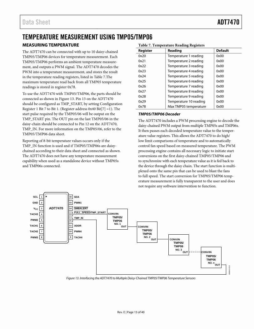
TEMPERATURE MEASUREMENT USING TMP05/TMP06 MEASURING TEMPERATURE The ADT7470 can be connected with up to 10 daisy-chained TMP05/TMP06 devices for temperature measurement. Each TMP05/TMP06 performs an ambient temperature measure-ment, and outputs a PWM signal. The ADT7470 decodes the PWM into a temperature measurement, and stores the result in the temperature reading registers, listed in Table 7.The maximum temperature read back from all TMP05 temperature readings is stored in register 0x78.
To use the ADT7470 with TMP05/TMP06, the parts should be connected as shown in Figure 13. Pin 13 on the ADT7470 should be configured as TMP_START, by setting Configuration Register 1 Bit 7 to Bit 1. (Register address 0x40 Bit[7] =1). The start pulse required by the TMP05/06 will be output on the TMP_START pin. The OUT pin on the last TMP05/06 in the daisy-chain should be connected to Pin 12 on the ADT7470, TMP_IN. For more information on the TMP05/06, refer to the TMP05/TMP06 data sheet.
Reporting of 8-bit temperature values occurs only if the TMP_IN function is used and if TMP05/TMP06s are daisy-chained according to their data sheet and connected as shown. The ADT7470 does not have any temperature measurement capability when used as a standalone device without TMP05s and TMP06s connected.
Table 7. Temperature Reading Registers Register Reading Default 0x20 Temperature 1 reading 0x00 0x21 Temperature 2 reading 0x00 0x22 Temperature 3 reading 0x00 0x23 Temperature 4 reading 0x00 0x24 Temperature 5 reading 0x00 0x25 Temperature 6 reading 0x00 0x26 Temperature 7 reading 0x00 0x27 Temperature 8 reading 0x00 0x28 Temperature 9 reading 0x00 0x29 Temperature 10 reading 0x00 0x78 Max TMP05 temperature 0x00
TMP05/TMP06 Decoder
The ADT7470 includes a PWM processing engine to decode the daisy-chained PWM output from multiple TMP05s and TMP06s. It then passes each decoded temperature value to the temper-ature value registers. This allows the ADT7470 to do high/ low limit comparisons of temperature and to automatically control fan speed based on measured temperature. The PWM processing engine contains all necessary logic to initiate start conversions on the first daisy-chained TMP05/TMP06 and to synchronize with each temperature value as it is fed back to the device through the daisy chain. The start function is multi-plexed onto the same pin that can be used to blast the fans to full speed. The start conversion for TMP05/TMP06 temp-erature measurement is fully transparent to the user and does not require any software intervention to function.
NO. 1
CONV/IN
OUT
NO. 2
CONV/IN
OUT
NO. 3
NO. n
CONV/IN
OUT CONV/IN
OUT
0468
4-0-
013
TMP05/TMP06
TMP05/TMP06
TMP05/TMP06
TMP05/TMP06
1
2
3
4
5
6
7
8
16
15
14
13
12
11
10
9
GND
VCC
TACH3
TACH2
TACH1
PWM2
SCL
PWM1
SMBALERT
PWM4
PWM3 TACH4
ADDR
TMP_IN
SDA
ADT7470FULL_SPEED/TMP_START
Figure 13. Interfacing the ADT7470 to Multiple Daisy-Chained TMP05/TMP06 Temperature Sensors
ADT7470 Data Sheet
Rev. E | Page 14 of 40
TEMPERATURE READBACK BY THE HOST The user cannot read the ADT7470 temperature register values if the ADT7470 is in the process of a temperature measurement. The user must wait until the data from all the TMP05s and TMP06s in the chain are received by the ADT7470 before reading these values. Otherwise, the temperature registers may store an incorrect value. It is recommended to wait at least 200 ms for each TMP05 and TMP06 in the chain. The recommended procedure is as follows:
1. Set Register 40 Bit[7] = 1. This starts the temperature measurements.
2. Wait 200 ms for each TMP05/TMP06 in the loop.
3. Set Register 40 Bit[7] = 0.
4. Read the temperature registers.
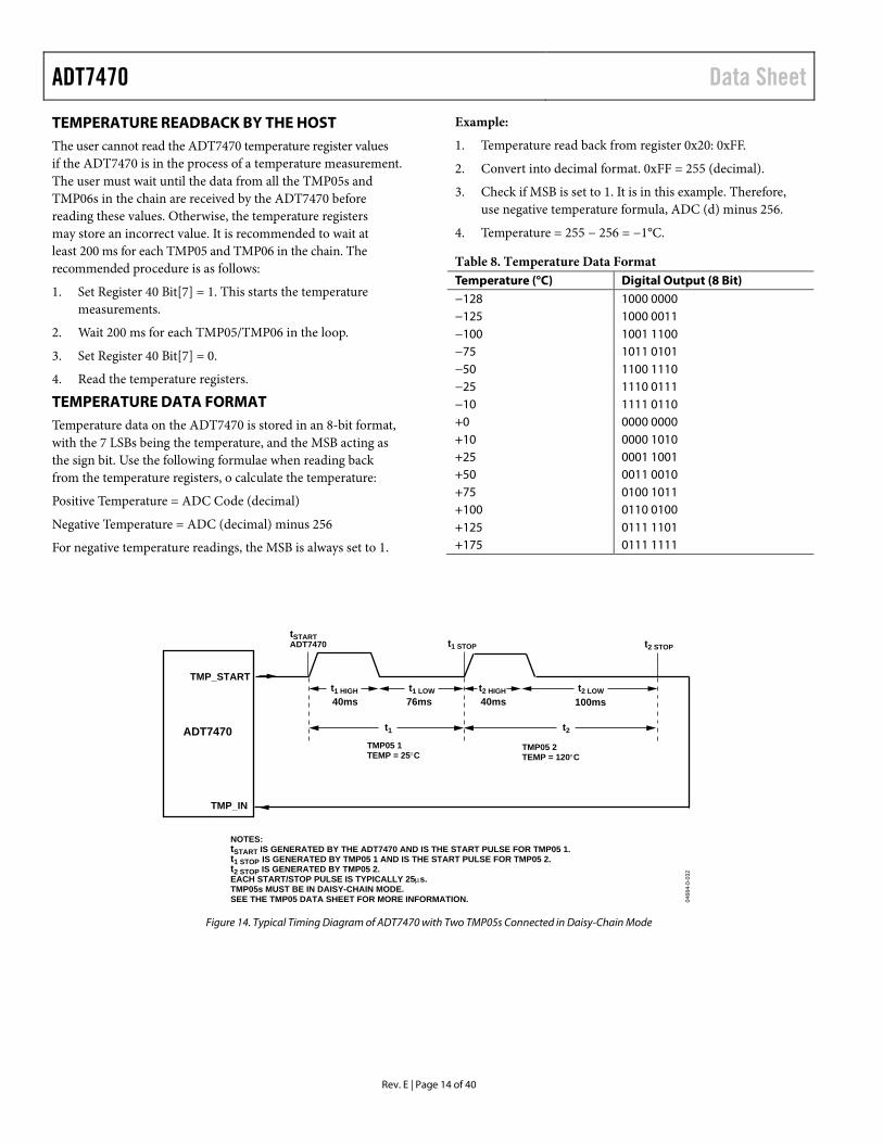
TEMPERATURE DATA FORMAT Temperature data on the ADT7470 is stored in an 8-bit format, with the 7 LSBs being the temperature, and the MSB acting as the sign bit. Use the following formulae when reading back from the temperature registers, o calculate the temperature:
Positive Temperature = ADC Code (decimal)
Negative Temperature = ADC (decimal) minus 256
For negative temperature readings, the MSB is always set to 1.
Example:
1. Temperature read back from register 0x20: 0xFF.
2. Convert into decimal format. 0xFF = 255 (decimal).
3. Check if MSB is set to 1. It is in this example. Therefore, use negative temperature formula, ADC (d) minus 256.
4. Temperature = 255 − 256 = −1°C.
Table 8. Temperature Data Format Temperature (°C) Digital Output (8 Bit) −128 1000 0000 −125 1000 0011 −100 1001 1100 −75 1011 0101 −50 1100 1110 −25 1110 0111 −10 1111 0110 +0 0000 0000 +10 0000 1010 +25 0001 1001 +50 0011 0010 +75 0100 1011 +100 0110 0100 +125 0111 1101 +175 0111 1111
40ms40ms 76ms 100ms
tSTARTADT7470 t1 STOP t2 STOP
TMP_START
TMP_IN
ADT7470TMP05 1TEMP = 25°C
TMP05 2TEMP = 120°C
NOTES:tSTART IS GENERATED BY THE ADT7470 AND IS THE START PULSE FOR TMP05 1.t1 STOP IS GENERATED BY TMP05 1 AND IS THE START PULSE FOR TMP05 2.t2 STOP IS GENERATED BY TMP05 2.EACH START/STOP PULSE IS TYPICALLY 25µs.TMP05s MUST BE IN DAISY-CHAIN MODE.SEE THE TMP05 DATA SHEET FOR MORE INFORMATION.
t2t1
t1 LOWt1 HIGH t2 LOWt2 HIGH04
684-
0-03
2
Figure 14. Typical Timing Diagram of ADT7470 with Two TMP05s Connected in Daisy-Chain Mode
Data Sheet ADT7470
Rev. E | Page 15 of 40
TEMPERATURE MEASUREMENT LIMITS High and low temperature limits can be individually set for each of the TMP05/06s that the ADT7470 is monitoring. The temperature limit registers are at address 0x44 to 0x57. The power-on default value for all TMP05/06 lower limits is −127°C (0x81). The power –on default value for all TMP05/06 upper limits is +127°C (0x7F). See Table 9 for details on the temperature limit registers.
If the temperature measured from a TMP05/06 exceeds the upper or lower limit, then a status bit in the Interrupt Status registers will be set to 1. See Table 12 and Table 13 for more details on the temperature status bits.
SMBALERT will assert is any temperature exceeds either the upper or lower limits. The temperature measurements can be masked as interrupt sources for SMBALERT using the interrupt mask registers, 0x72 and 0x73. See Table 14 and Table 15 for more details on the interrupt mask registers.
THERMAL ZONES FOR AUTOMATIC FAN CONTROL The ADT7470 can control up to four independent thermal zones with individual fans. The user can configure which TMP05 controls which fan via register 0x7C and 0x7D.For each of the four thermal zones, an individual TMP05, or the hottest TMP05 in the daisy chain, can control the fan. In a system with n TMP05s, it is possible to have 1 or n TMP05s controlling each fan.
Thermal Zone TMIN
For each of the four thermal zones, the user can configure the minimum temperature at which the fans run. Registers 0x6E to 0x71 should be configured with the minimum temperature for each thermal zone. When the temperature exceeds TMIN for that thermal zone, the fans run at minimum speed (PWMMIN). The fan speed increases to maximum speed (PWMMAX) at [TMIN + 20°C]. Fan on/off hysteresis is set at 4°C so that the fans turn off 4°C below the temperature at which they turn on. This prevents fan chatter in the system.
ADT7470 Data Sheet
Rev. E | Page 16 of 40
LIMIT AND STATUS REGISTERS LIMIT VALUES Associated with each measurement channel on the ADT7470 are high and low limits. These can form the basis of system status monitoring; a status bit can be set for any out-of-limit condition and be detected by polling the device. Alternatively, SMBALERT interrupts can be generated to automatically flag a service processor or microcontroller for out-of-limit conditions as they occur.
TEMPERATURE LIMITS Table 9 lists the 8-bit temperature limits on the ADT7470.
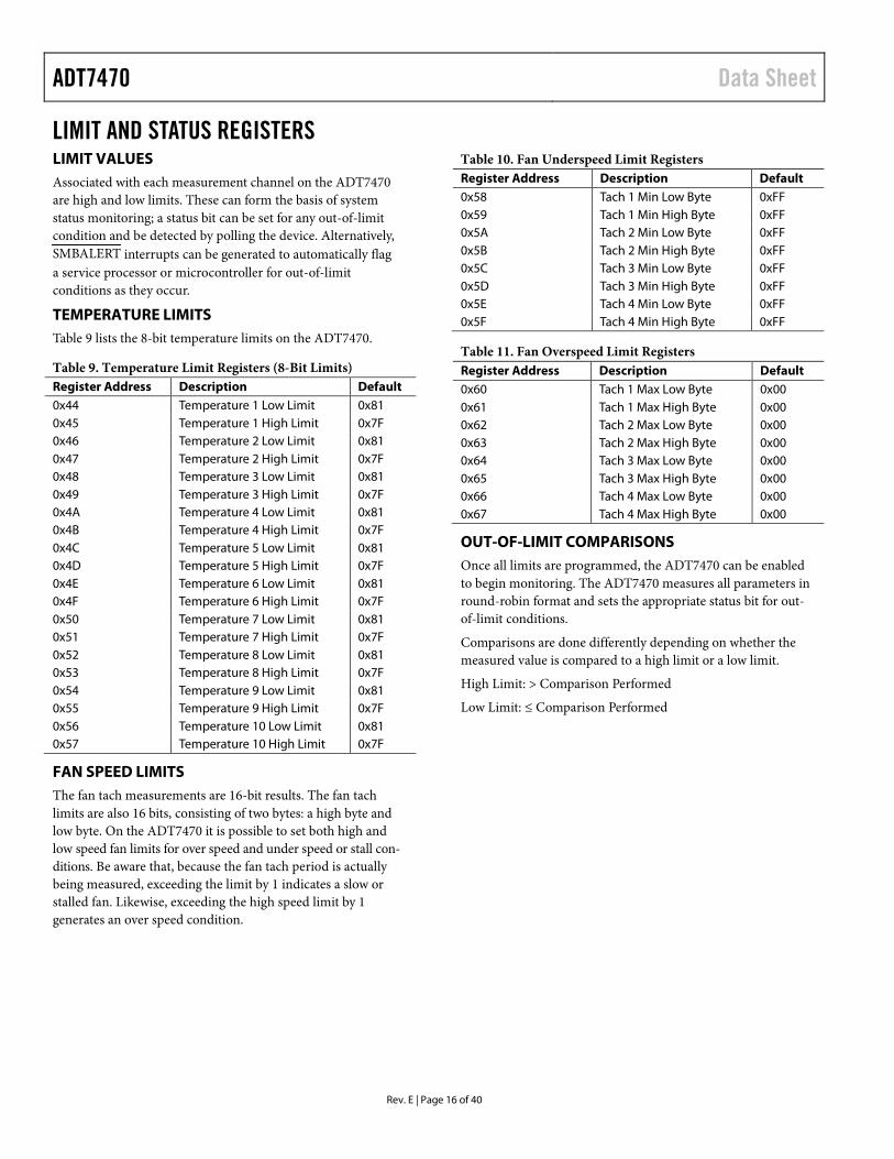
Table 9. Temperature Limit Registers (8-Bit Limits) Register Address Description Default 0x44 Temperature 1 Low Limit 0x81 0x45 Temperature 1 High Limit 0x7F 0x46 Temperature 2 Low Limit 0x81 0x47 Temperature 2 High Limit 0x7F 0x48 Temperature 3 Low Limit 0x81 0x49 Temperature 3 High Limit 0x7F 0x4A Temperature 4 Low Limit 0x81 0x4B Temperature 4 High Limit 0x7F 0x4C Temperature 5 Low Limit 0x81 0x4D Temperature 5 High Limit 0x7F 0x4E Temperature 6 Low Limit 0x81 0x4F Temperature 6 High Limit 0x7F 0x50 Temperature 7 Low Limit 0x81 0x51 Temperature 7 High Limit 0x7F 0x52 Temperature 8 Low Limit 0x81 0x53 Temperature 8 High Limit 0x7F 0x54 Temperature 9 Low Limit 0x81 0x55 Temperature 9 High Limit 0x7F 0x56 Temperature 10 Low Limit 0x81 0x57 Temperature 10 High Limit 0x7F
FAN SPEED LIMITS The fan tach measurements are 16-bit results. The fan tach limits are also 16 bits, consisting of two bytes: a high byte and low byte. On the ADT7470 it is possible to set both high and low speed fan limits for over speed and under speed or stall con-ditions. Be aware that, because the fan tach period is actually being measured, exceeding the limit by 1 indicates a slow or stalled fan. Likewise, exceeding the high speed limit by 1 generates an over speed condition.
Table 10. Fan Underspeed Limit Registers Register Address Description Default 0x58 Tach 1 Min Low Byte 0xFF 0x59 Tach 1 Min High Byte 0xFF 0x5A Tach 2 Min Low Byte 0xFF 0x5B Tach 2 Min High Byte 0xFF 0x5C Tach 3 Min Low Byte 0xFF 0x5D Tach 3 Min High Byte 0xFF 0x5E Tach 4 Min Low Byte 0xFF 0x5F Tach 4 Min High Byte 0xFF
Table 11. Fan Overspeed Limit Registers Register Address Description Default 0x60 Tach 1 Max Low Byte 0x00 0x61 Tach 1 Max High Byte 0x00 0x62 Tach 2 Max Low Byte 0x00 0x63 Tach 2 Max High Byte 0x00 0x64 Tach 3 Max Low Byte 0x00 0x65 Tach 3 Max High Byte 0x00 0x66 Tach 4 Max Low Byte 0x00 0x67 Tach 4 Max High Byte 0x00
OUT-OF-LIMIT COMPARISONS Once all limits are programmed, the ADT7470 can be enabled to begin monitoring. The ADT7470 measures all parameters in round-robin format and sets the appropriate status bit for out-of-limit conditions.
Comparisons are done differently depending on whether the measured value is compared to a high limit or a low limit.
High Limit: > Comparison Performed
Low Limit: ≤ Comparison Performed

Data Sheet ADT7470
Rev. E | Page 17 of 40
STATUS REGISTERS The results of limit comparisons are stored in Status Register 1 and Status Register 2. The status register bit for each channel reflects the status of the last measurement and limit comparison on that channel. If a measurement is within limits, the corre-sponding status register bit is cleared to 0. If the measurement is out of limit, the corresponding status register bit is set to 1.
The state of the various measurement channels can be polled by reading the status registers over the serial bus. When Bit 7 (OOL) of Status Register 1 (Register 0x41) is a 1, an out-of-limit event has been flagged in Status Register 2. This means that Status Register 2 must be read only when the OOL bit is set.
Reading the status registers clears the appropriate status bit as long as the error condition that caused the interrupt has cleared. Status register bits are sticky. Whenever a status bit is set, indicating an out-of-limit condition, it remains set even if the event that caused it has gone away (until read). The only way to clear the status bit is to read the status register when the event has gone away.
Interrupt status mask registers (Register 0x72 and Register 0x73) allow individual interrupt sources to be masked from causing an SMBALERT. However, if one of these masked interrupt sources goes out of limit, its associated status bit is still set in the interrupt status registers. This allows the device to be periodically polled to determine if an error condition has subsided, without unnecessarily tying up precious system resources handling interrupt service routines. The issue is that the device could potentially interrupt the system every monitoring cycle (< 1 sec) as long as a measurement parameter remains out of limit. Masking eliminates unwanted system interrupts.
The OOL bit (Register 0x41 Bit[7]), and the NORM bit (Register 0x42 Bit[3]) do not activate SMBALERT.
Table 12. Interrupt Status Register 1 (Register 0x41) Bit No. Mnemonic Description 7 OOL A 1 denotes that a bit in Status Register 2 is set and Status Register 2 should now be read. 6 R7T A 1 indicates that TMP05 Temperature 7 high or low limit has been exceeded. 5 R6T A 1 indicates that TMP05 Temperature 6 high or low limit has been exceeded. 4 R5T A 1 indicates that TMP05 Temperature 5 high or low limit has been exceeded. 3 R4T A 1 indicates that TMP05 Temperature 4 high or low limit has been exceeded. 2 R3T A 1 indicates that TMP05 Temperature 3 high or low limit has been exceeded. 1 R2T A 1 indicates that TMP05 Temperature 2 high or low limit has been exceeded. 0 R1T A 1 indicates that TMP05 Temperature 1 high or low limit has been exceeded.
Table 13. Interrupt Status Register 2 (Register 0x42) Bit No. Mnemonic Description 7 Fan 4 A 1 indicates that Fan 4 has dropped below minimum speed or is above maximum speed. 6 Fan 3 A 1 indicates that Fan 3 has dropped below minimum speed or is above maximum speed. 5 Fan 2 A 1 indicates that Fan 2 has dropped below minimum speed or is above maximum speed. 4 Fan 1 A 1 indicates that Fan 1 has dropped below minimum speed or is above maximum speed. 3 NORM A 1 indicates that the temperatures are below TMIN and that the fans are supposed to be off. 2 R10T A 1 indicates that TMP05 Temperature 10 high or low limit has been exceeded. 1 R9T A 1 indicates that TMP05 Temperature 9 high or low limit has been exceeded. 0 R8T A 1 indicates that TMP05 Temperature 8 high or low limit has been exceeded.

ADT7470 Data Sheet
Rev. E | Page 18 of 40
SMBALERT INTERRUPT
The ADT7470 can be polled for status, or an SMBALERT interrupt can be generated for out-of-limit conditions. Note how the SMBALERT output and status bits behave when writing interrupt handler software.
Figure 15 shows how the SMBALERT output and sticky status bits behave. Once a limit is exceeded, the corresponding status bit is set to 1. The status bit remains set until the error condition subsides the status register is read. The status bits are referred to as sticky because they remain set until read by software. This ensures that an out-of-limit event cannot be missed if software is polling the device periodically. The SMBALERT output remains low for the duration that a reading is out of limit until the status register is read. This has implications for how software handles the interrupt.
Handling SMBALERT Interrupts
To prevent the system from being tied up servicing interrupts, handle the SMBALERT interrupt as follows:
1. Detect the SMBALERT assertion.
2. Enter the interrupt handler.
3. Read the status registers to identify the interrupt source.
4. Mask the interrupt source by setting the appropriate mask bit in the interrupt mask registers (Register 0x72 and Register 0x73).
5. Take the appropriate action for a given interrupt source.
6. Exit the interrupt handler.
7. Periodically poll the status registers. If the interrupt status bit is cleared, reset the corresponding interrupt mask bit to 0. This causes the SMBALERT output and status bits to behave as shown in Figure 16.
"STICKY"STATUS
BIT
HIGH LIMIT
TEMPERATURE
SMBALERT
CLEARED ON READ(TEMP BELOW LIMIT)
TEMP BACK IN LIMIT(STATUS BIT STAYS SET)
0468
4-0-
020
Figure 15. SMBALERT and Status Bit Behavior
"STICKY"STATUS
BIT
HIGH LIMIT
TEMPERATURE
SMBALERT
CLEARED ON READ(TEMP BELOW LIMIT)
TEMP BACK IN LIMIT(STATUS BIT STAYS SET)
INTERRUPTMASK BIT SET
INTERRUPT MASK BITCLEARED
(SMBALERT RE-ENABLED) 0468
4-0-
021
Figure 16. How Masking the Interrupt Source Affects SMBALERT Output
Data Sheet ADT7470
Rev. E | Page 19 of 40
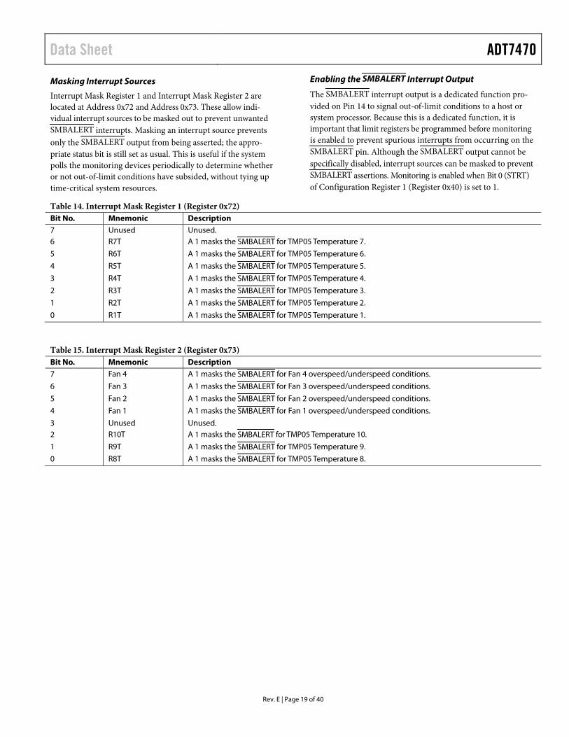
Masking Interrupt Sources
Interrupt Mask Register 1 and Interrupt Mask Register 2 are located at Address 0x72 and Address 0x73. These allow indi-vidual interrupt sources to be masked out to prevent unwanted SMBALERT interrupts. Masking an interrupt source prevents only the SMBALERT output from being asserted; the appro-priate status bit is still set as usual. This is useful if the system polls the monitoring devices periodically to determine whether or not out-of-limit conditions have subsided, without tying up time-critical system resources.
Enabling the SMBALERT Interrupt Output
The SMBALERT interrupt output is a dedicated function pro-vided on Pin 14 to signal out-of-limit conditions to a host or system processor. Because this is a dedicated function, it is important that limit registers be programmed before monitoring is enabled to prevent spurious interrupts from occurring on the SMBALERT pin. Although the SMBALERT output cannot be specifically disabled, interrupt sources can be masked to prevent SMBALERT assertions. Monitoring is enabled when Bit 0 (STRT) of Configuration Register 1 (Register 0x40) is set to 1.
Table 14. Interrupt Mask Register 1 (Register 0x72) Bit No. Mnemonic Description 7 Unused Unused. 6 R7T A 1 masks the SMBALERT for TMP05 Temperature 7.
5 R6T A 1 masks the SMBALERT for TMP05 Temperature 6.
4 R5T A 1 masks the SMBALERT for TMP05 Temperature 5.
3 R4T A 1 masks the SMBALERT for TMP05 Temperature 4.
2 R3T A 1 masks the SMBALERT for TMP05 Temperature 3.
1 R2T A 1 masks the SMBALERT for TMP05 Temperature 2.
0 R1T A 1 masks the SMBALERT for TMP05 Temperature 1.
Table 15. Interrupt Mask Register 2 (Register 0x73) Bit No. Mnemonic Description 7 Fan 4 A 1 masks the SMBALERT for Fan 4 overspeed/underspeed conditions.
6 Fan 3 A 1 masks the SMBALERT for Fan 3 overspeed/underspeed conditions.
5 Fan 2 A 1 masks the SMBALERT for Fan 2 overspeed/underspeed conditions.
4 Fan 1 A 1 masks the SMBALERT for Fan 1 overspeed/underspeed conditions.
3 Unused Unused. 2 R10T A 1 masks the SMBALERT for TMP05 Temperature 10.
1 R9T A 1 masks the SMBALERT for TMP05 Temperature 9.
0 R8T A 1 masks the SMBALERT for TMP05 Temperature 8.

ADT7470 Data Sheet
Rev. E | Page 20 of 40
FAN DRIVE USING PWM CONTROL The ADT7470 uses pulse-width modulation (PWM) to control fan speed. This relies on varying the duty cycle (or on/off ratio) of a square wave applied to the fan to vary the fan speed. Two main control schemes are used: low frequency and high fre-quency PWM.
Configuration Register 1 Bit[6], at address 0x40, configures the fan drive for high or low frequency operation. If this bit is set to 0, which is the default, high frequency fan drive is selected. If this bit is set to 1, low frequency fan drive is selected. All four PWM outputs on the ADT7470 have the same drive frequency.
HIGH FREQUENCY FAN DRIVE One of the important features of fan controllers is the PWM drive frequency. Most fans are driven asynchronously at low frequency (30 Hz to 100 Hz). Increasingly, the devices drive fans at greater than 20 kHz. These controllers are meant to drive 4-wire fans with PWM control built-in internal to the fan in Figure 17. The ADT7470 supports high frequency PWM (great than 20 kHz), as well as 1.4 kHz and other low frequency PWM. This allows the user to drive 3-wire or 4-wire fans.
If using 3-wire fans this mode, care should be taken to ensure that incomplete tach information does not occur at low PWM duty cycles, or short PWM pulse widths.
V
PWM
3.3V
10kΩ
TACH
ADT7470
12V
10kΩ
TACH
10kΩ
4.7kΩ
1N4148
0468
4-0-
024
GND
PWM_IN
Figure 17. Driving a 4-Wire Fan
LOW FREQUENCY FAN DRIVE For low frequency, low-side drive, the external circuitry required to drive a fan using PWM control is extremely simple. A single NMOS FET is the only drive device required. The specifications of the MOSFET depend on the maximum current required by the fan being driven. Typical notebook fans draw a nominal 170 mA; therefore, SOT devices can be used where board space is a concern. In desktops, fans can typically draw 250 mA to 300 mA each. If the user needs to drive several fans in parallel from a single PWM output or drive larger server fans, the MOSFET needs to handle the higher current requirements. The only other stipulation is that the MOSFET should have a gate voltage drive, VGS, less than 3.3 V, for direct interfacing to the PWM pin of the ADT7470. VGS of the chosen MOSFET can be greater than 3.3 V as long as the pull-up on its gate is tied to 5 V.
The MOSFET should also have a low on resistance to ensure that there is not significant voltage drop across the FET. This would reduce the voltage applied across the fan and, therefore, the maximum operating speed of the fan.
Figure 18 shows how a 3-wire fan can be driven using low frequency PWM control where the control method is low-side, low frequency switching.
Figure 18 shows the ideal interface when interfacing a tach signal from a 12 V fan (or greater voltage) to a 5 V (or less) logic device. In all cases, the tach signal from the fan must be kept below 5 V maximum to prevent damage to the ADT7470. The three resistors in Figure 18 ensure that the tach voltage is kept within safe levels for typical desktop and notebook systems.
12V
Q1NDT3055L
PWM
3.3V
10kΩ
12VFAN
TACH/AIN
ADT7470
12V
10kΩ
TACH10kΩ4.7kΩ
1N4148
0468
4-0-
022
Figure 18. Driving a 3-Wire Fan Using an N-Channel MOSFET

Data Sheet ADT7470
Rev. E | Page 21 of 40
Figure 19 shows a fan drive circuit using an NPN transistor such as a general-purpose MMBT2222. While these devices are inexpensive, they tend to have much lower current handling capabilities and higher on resistance than MOSFETs. When choosing a transistor, care should be taken to ensure that it meets the fan’s current requirements. This is the only major difference between a MOSFET and NPN transistor fan driver circuit.
When using transistors, ensure that the base resistor is chosen such that the transistor is fully saturated when the fan is powered on. Otherwise, there are power inefficiencies in the implementation.
12V
Q1MMBT2222PWM
3.3V
470Ω
12VFANTACH/AIN
ADT7470
12V
10kΩ
TACH10kΩ4.7kΩ
1N4148
0468
4-0-
023
Figure 19. Driving a 3-Wire Fan Using an NPN Transistor
Low Frequency
SETTING THE FAN DRIVE FREQUENCY Configuration Register 2 Bits[6:4] configure the fan drive frequency in both high and low frequency drive mode.
Table 16. Fan Drive Frequency Register 0x74[6:4]
High Frequency Drive (0x40[6] = 0)
Low Frequency Drive (0x40[6] = 1)
000 1.4 kHz 11 Hz 001 22.5 kHz 14.7 Hz 010 22.5 kHz 22.1 Hz 011 22.5 kHz 29.4 Hz 100 22.5 kHz 35.3 Hz 101 22.5 kHz 44.1 Hz 110 22.5 kHz 58.8 Hz 111 22.5 kHz 88.2 Hz
INVERTED PWM OUTPUT The PWM duty cycle can be inverted by writing to the PWM Configuration registers. If the PWM duty cycle is inverted, then a PWM duty cycle setting of 33% results in an output duty cycle of 66%, as the PWM waveform is inverted.
Table 17. PWM1/PWM2 Configuration (Register 0x68) Bit No. Mnemonic Description 5 INV1 0 = PWM1 duty cycle not inverted
(default). 1 = PWM1 duty cycle inverted.
4 INV2 0 = PWM2 duty cycle not inverted (default). 1 = PWM2 duty cycle inverted.
Table 18. PWM3/PWM4 Configuration (Register 0x69) Bit No. Mnemonic Description 5 INV3 0 = PWM3 duty cycle not inverted
(default). 1 = PWM3 duty cycle inverted.
4 INV4 0 = PWM4 duty cycle not inverted (default). 1 = PWM4 duty cycle inverted.
FAN FULL SPEED FUNCTION When Pin 13 is configured for full speed operation, pulling the pin low will cause all fans to run at the maximum PWM duty cycle. A Logic 1 is output on the PWM pins in this case.

ADT7470 Data Sheet
Rev. E | Page 22 of 40
FAN SPEED MEASUREMENT TACH INPUTS Pin 6, Pin 7, Pin 4, and Pin 9 are open-drain tach inputs intended for fan speed measurement.
Signal conditioning in the ADT7470 accommodates the slow rise and fall times typical of fan tachometer outputs. The maxi-mum input signal range is 0 V to 5 V, even where VCC is less than 5 V. If these inputs are supplied from fan outputs that exceed 0 V to 5 V, either resistive attenuation of the fan signal or diode clamping must be included to keep inputs within an acceptable range. Figure 20 to Figure 23 show circuits for most common fan tach outputs.
If the fan tach output has a resistive pull-up to VCC, it can be connected directly to the fan input, as shown in Figure 20.
12V
FAN SPEEDCOUNTER
TACH
PULLUP4.7kTYP
TACHOUTPUT
VCC
ADT7470
0468
4-0-
025
Figure 20. Fan with Tach Pull-Up to VCC
If the fan output has a resistive pull-up to 12 V (or other voltage greater than 5 V), the fan output can be clamped with a Zener diode, as shown in Figure 21. The Zener diode voltage should be chosen so that it is greater than VIH of the tach input but less than 5 V, allowing for the voltage tolerance of the Zener. A value of between 3 V and 5 V is suitable.
12V
FAN SPEEDCOUNTER
TACHTACHOUTPUT
ZD1*ZENER
PULLUP4.7kTYP
*CHOOSE ZD1 VOLTAGE APPROX. 0.8 VCC
VCC
ADT7470
0468
4-0-
026
Figure 21. Fan with Tach.
Pull-Up to voltage > 5 V, for example, 12 V clamped with Zener diode.
If the fan output has a resistive pull-up to 12 V (or other voltage greater than 5 V), the fan output can be clamped with a Zener diode, as shown in Figure 21. The Zener diode voltage should be chosen so that it is greater than VIH of the tach input but less than 5 V, allowing for the voltage tolerance of the Zener. A value of between 3 V and 5 V is suitable.
If the fan has a strong pull-up (less than 1 kΩ) to 12 V, or a totem-pole output, a series resistor can be added to limit the Zener current, as shown in Figure 22. Alternatively, a resistive attenuator can be used, as shown in Figure 23.
R1 and R2 should be chosen such that
2 V < VPULL-UP × R2/(RPULL-UP + R1 + R2) < 5 V
The fan inputs have an input resistance of nominally 160 kΩ to ground, which should be taken into account when calculating resistor values.
With a pull-up voltage of 12 V and pull-up resistor less than 1 kΩ, suitable values for R1 and R2 are 100 kΩ and 47 kΩ. This gives a high input voltage of 3.83 V.
12V
FAN SPEEDCOUNTER
TACHPULLUP
TYP. <1kOR TOTEM-POLE
ZD1ZENER*
R110k
TACHO/P
*CHOOSE ZD1 VOLTAGE APPROX. 0.8 VCC
VCC
ADT7470
0468
4-0-
027
Figure 22. Fan with Strong Tach.
Pull-Up to > VCC or Totem-Pole Output, Clamped with Zener and Resistor.
12V
FAN SPEEDCOUNTER
TACH
TACHOUTPUT
R1*
R2*
<1k
VCC
*SEE TEXT
ADT7470
0468
4-0-
028
Figure 23. Fan with Strong Tach.
Pull-Up to > VCC or Totem-Pole Output, Attenuated with R1/R2.
Pulse Stretching
Pulse stretching of the PWM output is performed automatically in low frequency fan drive mode, to ensure that sufficient tach readings are taken from the fan.
However, in high frequency fan drive mode, pulse stretching is disabled. If using 3-wire fans this mode, care should be taken to ensure that incomplete tach information does not occur at low PWM duty cycles, or short PWM pulse widths.
Disabling Tach measurement
The tach measurement for each fan can be disabled by writing to Configuration Register 2 Bits[3:0], at Address 0x74.
Data Sheet ADT7470
Rev. E | Page 23 of 40
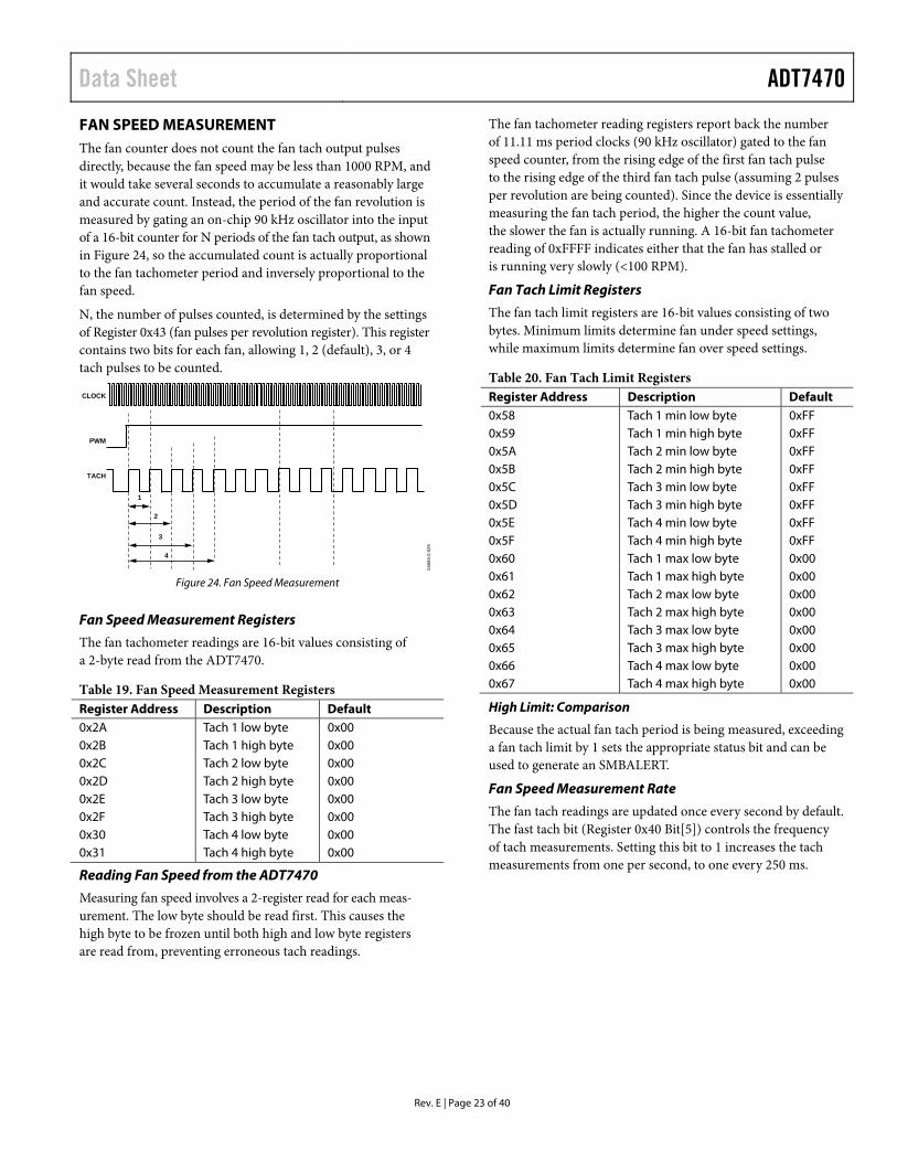
FAN SPEED MEASUREMENT The fan counter does not count the fan tach output pulses directly, because the fan speed may be less than 1000 RPM, and it would take several seconds to accumulate a reasonably large and accurate count. Instead, the period of the fan revolution is measured by gating an on-chip 90 kHz oscillator into the input of a 16-bit counter for N periods of the fan tach output, as shown in Figure 24, so the accumulated count is actually proportional to the fan tachometer period and inversely proportional to the fan speed.
N, the number of pulses counted, is determined by the settings of Register 0x43 (fan pulses per revolution register). This register contains two bits for each fan, allowing 1, 2 (default), 3, or 4 tach pulses to be counted.
CLOCK
PWM
TACH
1
2
3
4
0468
4-0-
029
Figure 24. Fan Speed Measurement
Fan Speed Measurement Registers
The fan tachometer readings are 16-bit values consisting of a 2-byte read from the ADT7470.
Table 19. Fan Speed Measurement Registers Register Address Description Default 0x2A Tach 1 low byte 0x00 0x2B Tach 1 high byte 0x00 0x2C Tach 2 low byte 0x00 0x2D Tach 2 high byte 0x00 0x2E Tach 3 low byte 0x00 0x2F Tach 3 high byte 0x00 0x30 Tach 4 low byte 0x00 0x31 Tach 4 high byte 0x00
Reading Fan Speed from the ADT7470
Measuring fan speed involves a 2-register read for each meas-urement. The low byte should be read first. This causes the high byte to be frozen until both high and low byte registers are read from, preventing erroneous tach readings.
The fan tachometer reading registers report back the number of 11.11 ms period clocks (90 kHz oscillator) gated to the fan speed counter, from the rising edge of the first fan tach pulse to the rising edge of the third fan tach pulse (assuming 2 pulses per revolution are being counted). Since the device is essentially measuring the fan tach period, the higher the count value, the slower the fan is actually running. A 16-bit fan tachometer reading of 0xFFFF indicates either that the fan has stalled or is running very slowly (<100 RPM).
Fan Tach Limit Registers
The fan tach limit registers are 16-bit values consisting of two bytes. Minimum limits determine fan under speed settings, while maximum limits determine fan over speed settings.
Table 20. Fan Tach Limit Registers Register Address Description Default 0x58 Tach 1 min low byte 0xFF 0x59 Tach 1 min high byte 0xFF 0x5A Tach 2 min low byte 0xFF 0x5B Tach 2 min high byte 0xFF 0x5C Tach 3 min low byte 0xFF 0x5D Tach 3 min high byte 0xFF 0x5E Tach 4 min low byte 0xFF 0x5F Tach 4 min high byte 0xFF 0x60 Tach 1 max low byte 0x00 0x61 Tach 1 max high byte 0x00 0x62 Tach 2 max low byte 0x00 0x63 Tach 2 max high byte 0x00 0x64 Tach 3 max low byte 0x00 0x65 Tach 3 max high byte 0x00 0x66 Tach 4 max low byte 0x00 0x67 Tach 4 max high byte 0x00
High Limit: Comparison
Because the actual fan tach period is being measured, exceeding a fan tach limit by 1 sets the appropriate status bit and can be used to generate an SMBALERT.
Fan Speed Measurement Rate
The fan tach readings are updated once every second by default. The fast tach bit (Register 0x40 Bit[5]) controls the frequency of tach measurements. Setting this bit to 1 increases the tach measurements from one per second, to one every 250 ms.

ADT7470 Data Sheet
Rev. E | Page 24 of 40
Calculating Fan Speed and Tachometer Limits
Assuming that the measured number of tach pulses per rotation corresponds to the number of pulses counted as set in register 0x43, fan speed is calculated by
Fan Speed (RPM) = (90,000 × 60)/Fan Tach Reading
where Fan Tach Reading is the 16-bit fan tachometer reading.
For example:
Tach 1 High Byte (Reg 0x2B) = 0x17
Tach 1 Low Byte (Reg 0x2A) = 0xFF
What is Fan 1 speed in RPM?
Fan 1 tach reading = 0x17FF = 6143 decimal
RPM = (f × 60)/Fan 1 tach reading
RPM = (90000 × 60)/6143
Fan Speed = 879 RPM
Calculate the tachometer maximum and minimum limits at 1000 RPM and 500 RPM as follows:
1000 RPM
(90,000 × 60)/1000 = 5400 decimal
5400 decimal = 1518 hex
Tach 1 maximum = 1518
500 RPM
(90,000 × 60)/500 = 10800 decimal
10800 decimal = 2A30 hex
Tach 1 minimum = 2A30
Fan Pulses per Revolution
Different fan models can output either 1, 2, 3, or 4 tach pulses per revolution. The number of tach pulses per rotation for each fan should be programmed into the fan pulses per revolution register (Register 0x43). If an incorrect value is programmed, then the fan speed cannot be determined using the equation in the Calculating Fan Speed section.
Alternatively, if the number of tach pulses per rotation is not know, this register can be used in determining the number of pulses/revolution output by a given fan. By plotting fan speed measurements at maximum speed with different pulses/ revolution settings, the smoothest graph with the lowest ripple determines the correct pulses/revolution value.

Data Sheet ADT7470
Rev. E | Page 25 of 40
MANUAL FAN SPEED CONTROL Manual fan speed control on the ADT7470 allows the user to control the PWM duty cycle for each fan via the registers. The ADT7470 powers-up in manual fan control mode, with all PWM duty cycles set to maximum. The PWM Configuration registers determine whether the fans are in manual or automatic fan control mode.
SETTING THE PWM DUTY CYCLE The ADT7470 allows the duty cycle of any PWM output to be manually adjusted. This can be useful if users want to change fan speed in software or want to adjust PWM duty cycle output for test purposes. The PWM current duty cycle registers (Register 0x32 to Register 0x35) can be written with 8-bit values in manual fan speed control mode to manually adjust the speeds of the cooling fans.
The PWM duty cycle for each output can be set anywhere from 0% to 100%, in steps of 0.39%.
The value to be programmed into the PWM Current Duty Cycle registers can be calculated as follows:
Value (decimal) = Desired PWM duty cycle/0.39
Example 1: For a PWM Duty Cycle of 50%
Value (decimal) = 50/0.39 = 128 decimal Value = 128 decimal or 80 hex
Example 2: For a PWM Duty Cycle of 33%
Value (decimal) = 33/0.39 = 85 decimal Value = 85 decimal or 54 hex
Table 21. PWM Current Duty Cycle Registers Register Address Description Default 0x32 PWM1 duty cycle 0xFF (100%) 0x33 PWM2 duty cycle 0xFF (100%) 0x34 PWM3 duty cycle 0xFF (100%) 0x35 PWM4 duty cycle 0xFF (100%)
Table 22.Fan Control Mode Configuration Register/Bit Mnenonic Description 0x68 Bit[6] BHVR2 This bit determines fan behavior for PWM2 output.
0 = Manual mode (PWM2 duty cycle controlled in software). 1 = Fastest speed calculated by all temperatures control PWM2 (automatic fan control mode).
0x68 Bit[7] BHVR1 This bit determines fan behavior for PWM1 output. 0 = Manual mode (PWM1 duty cycle controlled in software). 1 = Fastest speed calculated by all temperatures control PWM1 (automatic fan control mode).
0x69 Bit[6] BHVR4 This bit determines fan behavior for PWM4 output. 0 = Manual mode (PWM4 duty cycle controlled in software). 1 = Fastest speed calculated by all temperatures control PWM4 (automatic fan control mode).
0x69 Bit[7] BHVR3 This bit determines fan behavior for PWM3 output. 0 = Manual mode (PWM3 duty cycle controlled in software). 1 = Fastest speed calculated by all temperatures control PWM3 (automatic fan control mode).

ADT7470 Data Sheet
Rev. E | Page 26 of 40
AUTOMATIC FAN SPEED CONTROL In automatic fan speed control mode, fan speed automatically varies with temperature and without CPU intervention, once initial parameters are set up. The advantage is that when a system hangs, the user is guaranteed that the system is protected from overheating.
Automatic fan speed control mode is recommended for use only when temperatures > 8°C. In automatic fan control mode, if the temperature drops below 0°C, the fans automatically turn on.
For each thermal zone, when the temperature exceeds TMIN, the fans turn on at PWMMIN duty cycle. When the temperature reaches TMIN + 20°C, the fans increase in speed to PWMMAX.
To configure each fan into automatic fan control mode, the BHVR bit for that fan must be set to 1. See Table 22 for more details.
To control the fans in automatic fan control mode, a number of parameters for each fan should be set up. The PWM minimum and maximum duty cycles, as well as the minimum temperature at which each fan turns on, should be configured. Which TMP05 controls which fan also needs to be configured.
What follows are the automatic fan control configuration steps:
1. Put the fans into automatic fan control mode, by setting the BHVR bits for each fan to 1.
2. Determine which TMP05 is to control the fan, by configuring Registers 0x7C and 0x7D. Any TMP05, can control any fan, or the hottest TMP05 can control the fan.
3. Set the minimum temperature for each fan, by writing to Registers 0x6E to 0x70. When the temperature exceeds TMIN, the fan runs at PWMMIN.
4. Set PWMMIN, the minimum PWM duty cycle, by writing to Registers 0x6A to 0x6D.
5. Set PWMMAX, the maximum PWM duty cycle, by writing to registers 0x38 to 0x3B.
6. Write to the STRT bit in Configuration Register 1 (0x40 Bit[0]) to start the ADT7470 monitoring cycle. Set Bit 7 in this register to 1 to enable the TMP05 start pulse.
PWM Min Duty Cycle
The PWM min duty cycle registers, at address 0x6A to 0x6D, set the PWM duty cycle at which the fans turn on in automatic fan control mode.
The value to be programmed into the PWM Min Duty Cycle registers can be calculated as follows:
Value (decimal) = Desired PWM duty cycle/0.39
Example: For a PWM Min Duty Cycle of 30%
Value (decimal) = 30/0.39 = 77 decimal Value = 77 decimal or 4D hex
The PWM min duty cycle registers have a default value of 0x80, which corresponds to a duty cycle of 50% on the PWM output pin.
PWN Max Duty Cycle
For each fan, the maximum PWM duty cycle can be set by writing to Registers 0x38 to 0x3B.
The value to be programmed into the PWM max duty cycle registers can be calculated as follows:
Value (decimal) = Desired PWM duty cycle/0.39
Example: For a PWM Max Duty Cycle of 90%
Value (decimal) = 90/0.39 = 230 decimal Value = 230 decimal or E6 hex
The PWM max duty cycle registers have a default value of 0xFF, which corresponds to a Logic 1 on the PWM output pin.
PWM Current Duty Cycle
In automatic fan control mode, the current PWM duty cycle for each fan is recorded in the PWM current duty cycle registers, (0x02 to 0x35). By reading these registers, the user can keep track of the current duty cycle on each PWM output. During fan start up, these registers report back 0x00.
If the FULLSPEED pin is activated, to blast the fans to the maximum possible PWM ( logic high), the PWM current duty cycle register is not updated.

Data Sheet ADT7470
Rev. E | Page 27 of 40
REGISTER MAP Table 23. ADT7470 Register Map Address R/W Description Default Lockable
0x20 R Temperature 1 Reading 0x00 0x21 R Temperature 2 Reading 0x00 0x22 R Temperature 3 Reading 0x00 0x23 R Temperature 4 Reading 0x00 0x24 R Temperature 5 Reading 0x00 0x25 R Temperature 6 Reading 0x00 0x26 R Temperature 7 Reading 0x00 0x27 R Temperature 8 Reading 0x00 0x28 R Temperature 9 Reading 0x00 0x29 R Temperature 10 Reading 0x00
0x2A R Tach 1 Low Byte 0xFF 0x2B R Tach 1 High Byte 0xFF 0x2C R Tach 2 Low Byte 0xFF 0x2D R Tach 2 High Byte 0xFF 0x2E R Tach 3 Low Byte 0xFF 0x2F R Tach 3 High Byte 0xFF 0x30 R Tach 4 Low Byte 0xFF 0x31 R Tach 4 High Byte 0xFF
0x32 R/W PWM1 Current Duty Cycle 0xFF 0x33 R/W PWM2 Current Duty Cycle 0xFF 0x34 R/W PWM3 Current Duty Cycle 0xFF 0x35 R/W PWM4 Current Duty Cycle 0xFF
0x36 R Reserved 0x00 0x37 R/W ADI Test Register 1 0x00 y
0x38 R/W PWM1 Max Duty Cycle 0xFF 0x39 R/W PWM2 Max Duty Cycle 0xFF 0x3A R/W PWM3 Max Duty Cycle 0xFF 0x3B R/W PWM4 Max Duty Cycle 0xFF
0x3C R/W ADI Test Register 2 0x00 y
0x3D R Device ID Register 0x70 0x3E R Company ID Number 0x41 0x3F R Revision Number 0x02
0x40 R/W Configuration Register 1 0x01 0x41 R Interrupt Status Register 1 0xXX 0x42 R Interrupt Status Register 2 0xXX 0x43 R/W Fan Pulses per Revolution 0x55
0x44 R/W Temperature 1 Low Limit 0x81 0x45 R/W Temperature 1 High Limit 0x7F 0x46 R/W Temperature 2 Low Limit 0x81 0x47 R/W Temperature 2 High Limit 0x7F 0x48 R/W Temperature 3 Low Limit 0x81 0x49 R/W Temperature 3 High Limit 0x7F 0x4A R/W Temperature 4 Low Limit 0x81 0x4B R/W Temperature 4 High Limit 0x7F 0x4C R/W Temperature 5 Low Limit 0x81 0x4D R/W Temperature 5 High Limit 0x7F 0x4E R/W Temperature 6 Low Limit 0x81 0x4F R/W Temperature 6 High Limit 0x7F 0x50 R/W Temperature 7 Low Limit 0x81 0x51 R/W Temperature 7 High Limit 0x7F 0x52 R/W Temperature 8 Low Limit 0x81 0x53 R/W Temperature 8 High Limit 0x7F

ADT7470 Data Sheet
Rev. E | Page 28 of 40
Address R/W Description Default Lockable
0x54 R/W Temperature 9 Low Limit 0x81 0x55 R/W Temperature 9 High Limit 0x7F 0x56 R/W Temperature 10 Low Limit 0x81 0x57 R/W Temperature 10 High Limit 0x7F
0x58 R/W Tach 1 Min Low Byte 0xFF 0x59 R/W Tach 1 Min High Byte 0xFF 0x5A R/W Tach 2 Min Low Byte 0xFF 0x5B R/W Tach 2 Min High Byte 0xFF 0x5C R/W Tach 3 Min Low Byte 0xFF 0x5D R/W Tach 3 Min High Byte 0xFF 0x5E R/W Tach 4 Min Low Byte 0xFF 0x5F R/W Tach 4 Min High Byte 0xFF 0x60 R/W Tach 1 Max Low Byte 0x00 0x61 R/W Tach 1 Max High Byte 0x00 0x62 R/W Tach 2 Max Low Byte 0x00 0x63 R/W Tach 2 Max High Byte 0x00 0x64 R/W Tach 3 Max Low Byte 0x00 0x65 R/W Tach 3 Max High Byte 0x00 0x66 R/W Tach 4 Max Low Byte 0x00 0x67 R/W Tach 4 Max High Byte 0x00
0x68 R/W PWM1/2 Config Register 0x00 y 0x69 R/W PWM3/4 Config Register 0x00 y 0x6A R/W PWM1 Min Duty Cycle 0x80 y 0x6B R/W PWM2 Min Duty Cycle 0x80 y 0x6C R/W PWM3 Min Duty Cycle 0x80 y 0x6D R/W PWM4 Min Duty Cycle 0x80 y
0x6E R/W Temperature 1 TMIN 0x5A 0x6F R/W Temperature 2 TMIN 0x5A 0x70 R/W Temperature 3 TMIN 0x5A 0x71 R/W Temperature 4 TMIN 0x5A
0x72 R/W Interrupt Mask 1 Register 0x00 0x73 R/W Interrupt Mask 2 Register 0x00
0x74 R/W Configuration Register 2 0x00
0x75 R/W Reserved. Do not write to this register. 0x00 0x76 R/W Reserved. Do not write to this register. 0x00 0x77 R/W ADI Test Register 3 0x00 y
0x78 R Max TMP05 Temperature 0x00
0x79 R/W Reserved. Do not write to this register. 0x00 0x7A R/W Reserved. Do not write to this register. 0x00 0x7B R/W Reserved. Do not write to this register. 0x00
0x7C R/W TMP05 Zone Select 1 0x00 0x7D R/W TMP05 Zone Select 2 0x00
0x7E R/W Reserved. Do not write to this register. 0x00 0x7F R/W GPIO Enable 0x00 0x80 R/W GPIO Config 0x00 0x81 R GPIO Status 0x00
Data Sheet ADT7470
Rev. E | Page 29 of 40
DETAILED REGISTER DESCRIPTIONS Table 24. Register 0x20 to Register 0x29. Temperature Reading Registers (Power-On Default = 0x00). Register Address Read/Write Description Comments 0x20 Read-only 8-bit Temperature 1 reading (from TMP05 sensor). Bit[7] = Sign bit, indicates if temperature is positive or 0x21 Read-only 8-bit Temperature 2 reading (from TMP05 sensor). negative 0x22 Read-only 8-bit Temperature 3 reading (from TMP05 sensor). Bits[6:0] = temperature result 0x23 Read-only 8-bit Temperature 4 reading (from TMP05 sensor). 0x24 Read-only 8-bit Temperature 5 reading (from TMP05 sensor). To calculate the temperature: 0x25 Read-only 8-bit Temperature 6 reading (from TMP05 sensor). Positive Temperature = ADC Code (decimal) 0x26 Read-only 8-bit Temperature 2 reading (from TMP05 sensor). Negative Temperature = ADC (decimal) minus 256 0x27 Read-only 8-bit Temperature 3 reading (from TMP05 sensor). 0x28 Read-only 8-bit Temperature 4 reading (from TMP05 sensor). 0x29 Read-only 8-bit Temperature 5 reading (from TMP05 sensor).
Readings from daisy-chained TMP05 are processed and loaded into the temperature reading registers.
Table 25. Register 0x2A to Register 0x31. Fan Tach Reading Registers (Power-On Default = 0x00). Register Address Read/Write Description 0x2A Read-only Tach 1 low byte (8 MSBs of reading). 0x2B Read-only Tach 1 high byte (8 LSBs of reading). 0x2C Read-only Tach 2 high byte (8 MSBs of reading). 0x2D Read-only Tach 2 low byte (8 LSBs of reading). 0x2E Read-only Tach 3 high byte (8 MSBs of reading). 0x2F Read-only Tach 3 low byte (8 LSBs of reading). 0x30 Read-only Tach 4 high byte (8 MSBs of reading). 0x31 Read-only Tach 4 low byte (8 LSBs of reading).
The fan tach reading registers shown in Table 25 count the number of 11.11 µs periods (based on an internal 90 kHz clock) that occur between a number of consecutive fan tach pulses (default = 2). The number of tach pulses used to count can be changed using the fan pulses per revolution register (Register 0x43). This allows the fan speed to be accurately measured. Because a valid fan tachometer reading requires that two bytes are read, the low byte must be read first. Both the low and high bytes are then frozen until read. At power-on, these registers contain 0x0000 until such time as the first valid fan tach measurement is read in to these registers. This prevents false interrupts from occurring while the fans are spinning up.
A count of 0xFFFF indicates that a fan is
• Stalled or blocked (object jamming the fan).
• Failed (internal circuitry destroyed).
• Not populated. The ADT7470 expects to see a fan connected to each tach. If a fan is not connected to that tach, its tach minimum high and low byte are set to 0xFFFF.
Table 26. Register 0x32 to Register 0x35. Current PWM Duty Cycle Registers (Power-On Default = 0xFF). Register Address Read/Write Description 0x32 Read/Write PWM1 current duty cycle (0% to 100% duty cycle = 0x00 to 0xFF). 0x33 Read/Write PWM2 current duty cycle (0% to 100% duty cycle = 0x00 to 0xFF). 0x34 Read/Write PWM3 current duty cycle (0% to 100% duty cycle = 0x00 to 0xFF). 0x35 Read/Write PWM4 current duty cycle (0% to 100% duty cycle = 0x00 to 0xFF).
The current PWM duty cycle registers, shown in Table 26, reflect the PWM duty cycle driving each fan at any given time. When in automatic fan speed control mode, the ADT7470 reports the PWM duty cycles back through these registers. The PWM duty cycle values vary according to temperature in automatic fan speed control mode. During fan startup, these registers report back 0x00. In manual fan control mode, the PWM duty cycle outputs can be set to any duty cycle value by writing to these registers.
ADT7470 Data Sheet
Rev. E | Page 30 of 40
Table 27. Register 0x38 to Register 0x3B. PWM Max Duty Cycle Registers (Power-On Default = 0xFF). Register Address Read/Write Description 0x38 Read/Write PWM1 max duty cycle: PWM1 Min duty cycle value (register 0x6A) to 100% duty cycle. 0x39 Read/Write PWM2 max duty cycle: PWM2 Min duty cycle value (register 0x6B) to 100% duty cycle. 0x3A Read/Write PWM3 max duty cycle: PWM3 Min duty cycle value (register 0x6C) to 100% duty cycle. 0x3B Read/Write PWM4 max duty cycle: PWM4 Min duty cycle value (register 0x6D) to 100% duty cycle.
Table 28. Register 0x3D. Device ID Register (Power-On Default = 0x70). Register Address Read/Write Description 0x3D Read only Device ID.
The device ID register contains the ADT7470 device ID value as a means of identifying the part over the bus.
Table 29. Register 0x3E. Company ID Register (Power-On Default = 0x41). Register Address Read/Write Description 0x3E Read only Company ID.
The company ID register contains 0x41, the manufacturer ID number representative of the Analog Devices, Inc. product.
Table 30. Register 0x3F. Revision Register (Power-On Default = 0x02). Register Address Read/Write Description 0x3F Read only Revision Register.
The revision register contains the revision number of the ADT7470.
Table 31. Register 0x40. Configuration Register 1 (Power-On Default = 0x01). Bit Name Read/Write Description [0] STRT Read/Write Logic 1 enables monitoring and PWM control outputs based on the limit settings
programmed. Logic 0 disables monitoring and PWM control based on the default power-up limit settings. The limit values programmed are preserved even if a Logic 0 is written to this bit and the default settings are enabled.
[1] Reserved Read/Write Reserved. Write 0 to this bit. [2] Reserved Read/Write Reserved. Write 0 to this bit. [3] TODIS Read/Write Writing a 1 disables SMBus timeout. [4] LOCK Write Once Once this bit is set, all lockable registers become read-only and cannot be modified until the
ADT7470 is powered down and powered up again. [5] FST_TCH Read/Write Enable Fast Tach measurement.
0 = Tach measurement rate is 1 measurement per second 1= Tach measurement rate is 1 measurement every 250ms
[6] HF_LF Read/Write This bit switches between high frequency and low frequency fan drive. 0 (default) = high frequency fan drive (1.4 kHz or 22.5 kHz. See Configuration Register 2, Register 0x74, Bits [6:4]) in Table 44. 1 = low frequency fandrive (frequency determined by Configuration Register 2, Register 0x74, Bits[6:4]) in Table 44.
[7] T05_STB Read/Write Select configuration for Pin 13. 0 (default) =FULL SPEED input. 1 = TMP05 start pulse output.
Data Sheet ADT7470
Rev. E | Page 31 of 40
Table 32. Register 0x41. Interrupt Status Register 1 (Power-On Default = 0x00). Bit Name Read/Write Description [0] R1T Read-only A 1 indicates that the Remote 1 temperature high or low limit has been exceeded.
This bit is cleared on a read of the status register only if the error condition has subsided. [1] R2T Read-only A 1 indicates that the Remote 2 temperature high or low limit has been exceeded.
This bit is cleared on a read of the status register only if the error condition has subsided. [2] R3T Read-only A 1 indicates that the Remote 3 temperature high or low limit has been exceeded.
This bit is cleared on a read of the status register only if the error condition has subsided. [3] R4T Read-only A 1 indicates that the Remote 4 temperature high or low limit has been exceeded.
This bit is cleared on a read of the status register only if the error condition has subsided. [4] R5T Read-only A 1 indicates that the Remote 5 temperature high or low limit has been exceeded.
This bit is cleared on a read of the status register only if the error condition has subsided. [5] R6T Read-only A 1 indicates that the Remote 6 temperature high or low limit has been exceeded.
This bit is cleared on a read of the status register only if the error condition has subsided. [6] R7T Read-only A 1 indicates that the Remote 7 temperature high or low limit has been exceeded.
This bit is cleared on a read of the status register only if the error condition has subsided. [7] OOL Read-only A 1 indicates that an out-of-limit event has been latched in Status Register 2. This bit is a
logical OR of all status bits in Status Register 2. Software can test this bit in isolation to determine whether any of the temperature or fan speed readings represented by Status Register 2 are out of limit. This saves the need to read Status Register 2 every interrupt or polling cycle.
Table 33. Register 0x42. Interrupt Status Register 2 (Power-On Default = 0x00). Bit Name Read/Write Description [0] R8T Read-only A 1 indicates that the Remote 8 temperature high or low limit has been exceeded.
This bit is cleared on a read of the status register only if the error condition has subsided. [1] R9T Read-only A 1 indicates that the Remote 9 temperature high or low limit has been exceeded.
This bit is cleared on a read of the status register only if the error condition has subsided. [2] R10T Read-only A 1 indicates that the Remote 10 temperature high or low limit has been exceeded.
This bit is cleared on a read of the status register only if the error condition has subsided. [3] NORM Read-only A 1 indicates that the measured temperatures are normal (below TMIN), and the fans should
be off. [4] Fan 1 Read-only A 1 indicates that Fan 1 has gone above max speed or dropped below min speed. [5] Fan 2 Read-only A 1 indicates that Fan 2 has gone above max speed or dropped below min speed. [6] Fan 3 Read-only A 1 indicates that Fan 3 has gone above max speed or dropped below min speed. [7] Fan 4 Read-only A 1 indicates that Fan 4 has gone above max speed or dropped below min speed.
ADT7470 Data Sheet
Rev. E | Page 32 of 40
Table 34. Register 0x43. Fan Pulses per Revolution Register (Power-On Default = 0x55). Bit Name Read/Write Description [1:0] Fan 1 Read/Write Sets the number of pulses to be counted when measuring Fan 1 speed.
Can be used to determine fan’s pulses per revolution number for unknown fan type. Pulses Counted 00 = 1 01 = 2 (default) 10 = 3 11 = 4 [3:2] Fan 2 Read/Write Sets the number of pulses to be counted when measuring Fan 2 speed.
Can be used to determine fan’s pulses per revolution number for unknown fan type. Pulses Counted 00 = 1 01 = 2 (default) 10 = 3 11 = 4 [5:4] Fan 3 Read/Write Sets the number of pulses to be counted when measuring Fan 3 speed.
Can be used to determine fan’s pulses per revolution for unknown fan type. Pulses Counted 00 = 1 01 = 2 (default) 10 = 3 11 = 4 [7:6] Fan 4 Read/Write Sets the number of pulses to be counted when measuring Fan 4 speed. Can be used to determine fan’s
pulses per revolution for unknown fan type. Pulses Counted 00 = 1 01 = 2 (default) 10 = 3 11 = 4
Table 35. Register 0x44 to Register 0x57. Temperature Limit Registers. Register Address Read/Write Description Power-On Default 0x44 Read/Write Temperature 1 low limit 0x81 0x45 Read/Write Temperature 1 high limit 0x7F 0x46 Read/Write Temperature 2 low limit 0x81 0x47 Read/Write Temperature 2 high limit 0x7F 0x48 Read/Write Temperature 3 low limit 0x81 0x49 Read/Write Temperature 3 high limit 0x7F 0x4A Read/Write Temperature 4 low limit 0x81 0x4B Read/Write Temperature 4 high limit 0x7F 0x4C Read/Write Temperature 5 low limit 0x81 0x4D Read/Write Temperature 5 high limit 0x7F 0x4E Read/Write Temperature 6 low limit 0x81 0x4F Read/Write Temperature 6 high limit 0x7F 0x50 Read/Write Temperature 7 low limit 0x81 0x51 Read/Write Temperature 7 high limit 0x7F 0x52 Read/Write Temperature 8 low limit 0x81 0x53 Read/Write Temperature 8 high limit 0x7F 0x54 Read/Write Temperature 9 low limit 0x81 0x55 Read/Write Temperature 9 high limit 0x7F 0x56 Read/Write Temperature 10 low limit 0x81 0x57 Read/Write Temperature 10 high limit 0x7F
Exceeding any of the temperature limits shown in Table 35 by 1°C causes the appropriate status bit to be set in the interrupt status registers.
High limits: An interrupt is generated when a value exceeds its high limit (> comparison). Low limits: An interrupt is generated when a value is equal to or below its low limit (≤ comparison).

Data Sheet ADT7470
Rev. E | Page 33 of 40
Table 36. Register 0x58 to Register 0x67. Fan Tachometer Limit Registers. Register Address Read/Write Description Power-On Default 0x58 Read/Write Tach 1 min low byte 0xFF 0x59 Read/Write Tach 1 min high byte 0xFF 0x5A Read/Write Tach 2 min low byte 0xFF 0x5B Read/Write Tach 2 min high byte 0xFF 0x5C Read/Write Tach 3 min low byte 0xFF 0x5D Read/Write Tach 3 min high byte 0xFF 0x5E Read/Write Tach 4 min low byte 0xFF 0x5F Read/Write Tach 4 min high byte 0xFF 0x60 Read/Write Tach 1 max low byte 0x00 0x61 Read/Write Tach 1 max high byte 0x00 0x62 Read/Write Tach 2 max low byte 0x00 0x63 Read/Write Tach 2 max high byte 0x00 0x64 Read/Write Tach 3 max low byte 0x00 0x65 Read/Write Tach 3 max high byte 0x00 0x66 Read/Write Tach 4 max low byte 0x00 0x67 Read/Write Tach 4 max high byte 0x00
Exceeding any of the tach min limit registers shown in Table 36 by 1 indicates that the fan is running too slowly or has stalled. The appropriate status bit is set in Interrupt Status Register 2 to indicate the fan failure. Exceeding any of the tach max limit registers by 1 indicates that the fan is too fast. The appropriate status bit is set in Interrupt Status Register 2 to indicate the fan failure.
Table 37. Register 0x68. PWM1/PWM2 Configuration Register (Power-On Default = 0x00). Bit Name Read/Write Description [0] N/A Set to 0 (default). [1] N/A Set to 0 (default). [2] N/A Set to 0 (default). [3] N/A Set to 0 (default). [4] INV2 Read/Write Setting this bit to 1 inverts the PWM2 output. Default = 0. [5] INV1 Read/Write Setting this bit to 1 inverts the PWM1 output. Default = 0. [6] BHVR2 Read/Write This bit assigns fan behavior for PWM2 output.
0 = manual fan control mode (PWM duty cycle controlled in software). 1 = automatic fan control mode
[7] BHVR1 Read/Write This bit assigns fan behavior for PWM1 output. 0 = manual fan control mode (PWM duty cycle controlled in software). 1 = automatic fan control mode.
ADT7470 Data Sheet
Rev. E | Page 34 of 40
Table 38. Register 0x69. PWM3/PWM4 Configuration Register (Power-On Default = 0x00). Bit Name Read/Write Description [0] N/A Set to 0 (default). [1] N/A Set to 0 (default). [2] N/A Set to 0 (default). [3] N/A Set to 0 (default). [4] INV4 Read/Write Setting this bit to 1 inverts the PWM4 output. Default = 0 [5] INV3 Read/Write Setting this bit to 1 inverts the PWM3 output. Default = 0 [6] BHVR4 Read/Write This bit assigns fan behavior for PWM4 output.
0 = manual fan control mode (PWM duty cycle controlled in software). 1 = (automatic fan control mode.
[7] BHVR3 Read/Write This bit assigns fan behavior for PWM3 output. 0 = manual fan control mode (PWM duty cycle controlled in software). 1 = automatic fan control mode.
Table 39. Register 0x6A to Register 0x6D. PWMMIN Duty Cycle Registers (Power-On Default = 0x80 (50% Duty Cycle). Register Address Read/Write Description 0x6A Read/Write PWM1 min duty cycle. 0x6B Read/Write PWM2 min duty cycle. 0x6C Read/Write PWM3 min duty cycle. 0x6D Read/Write PWM4 min duty cycle.
Table 40. PWMMIN Duty Cycle Registers Detailed Description Bit Name Read/Write Description [7:0] PWM Duty Cycle Read/Write These bits define the PWNMIN duty cycle for PWMx (x = 1 to 4). 0x00 = 0% duty cycle (fan off ). 0x40 = 25% duty cycle. 0x80 = 50% duty cycle. 0xFF = 100% PMW max duty cycle (full fan speed).
Table 41. Register 0x6E to Register 0x71. TMIN Registers (Power-On Default = 0x5A (90°C)). Register Address Read/Write Description 0x6E Read/Write Temperature 1 TMIN. 0x6F Read/Write Temperature 2 TMIN. 0x70 Read/Write Temperature 3 TMIN. 0x71 Read/Write Temperature 4 TMIN.
Table 41 shows the TMIN registers for each thermal zone. When the temperature measured exceeds TMIN, the appropriate fan runs at minimum speed (PWMMIN). They increase to maximum speed (PWMMAX) at TMIN + 20°C.

Data Sheet ADT7470
Rev. E | Page 35 of 40
Table 42. Register 0x72. Interrupt Mask Register 1 (Power-On Default = 0x00). Bit Name Read/Write Description [7] Not in use Read/Write Not in use. Write 0 to this bit. [6] R7T Read/Write A 1 masks the Temperature 7 value from generating an interrupt on the SMBALERT
output. The R1T bit is set as normal in the status register for out-of-limit conditions. [5] R6T Read/Write A 1 masks the Temperature 6 value from generating an interrupt on the SMBALERT
output. The R2T bit is set as normal in the status register for out-of-limit conditions. [4] R5T Read/Write A 1 masks the Temperature 5 value from generating an interrupt on the SMBALERT
output. The R3T bit is set as normal in the status register for out-of-limit conditions. [3] R4T Read/Write A 1 masks the Temperature 4 value from generating an interrupt on the SMBALERT
output. The R4T bit is set as normal in the status register for out-of-limit conditions. [2] R3T Read/Write A 1 masks the Temperature 3 value from generating an interrupt on the SMBALERT
output. The R5T bit is set as normal in the status register for out-of-limit conditions. [1] R2T Read/Write A 1 masks the Temperature 2 value from generating an interrupt on the SMBALERT
output. The R6T bit is set as normal in the status register for out-of-limit conditions. [0] R1T Read/Write A 1 masks the Temperature 1 value from generating an interrupt on the SMBALERT
output. The R7T bit is set as normal in the status register for out-of-limit conditions.
Table 43. Register 0x73. Interrupt Mask Register 2 (Power-On Default = 0x00). Bit Name Read/Write Description [7] Fan 4 Read/Write A 1 masks the Fan 4 value from generating an interrupt on the SMBALERT output.
The Fan 4 bit is set as normal in the status register for out-of-limit conditions. [6] Fan 3 Read/Write A 1 masks the Fan 3 value from generating an interrupt on the SMBALERT output.
The Fan 3 bit is set as normal in the status register for out-of-limit conditions. [5] Fan 2 Read/Write A 1 masks the Fan 2 value from generating an interrupt on the SMBALERT output.
The Fan 2 bit is set as normal in the status register for out-of-limit conditions. [4] Fan 1 Read/Write A 1 masks the Fan 1 value from generating an interrupt on the SMBALERT output.
The Fan 1 bit is set as normal in the status register for out-of-limit conditions. [3] Daisy chain Read/Write A 1 masks the pulsing of the SMBALERTwhile enabling daisy chain, writing to Bit [7]
Register 0x40. [2] R10T Read/Write A 1 masks the Temperature 10 value from generating an interrupt on the SMBALERT
output. The R10T bit is set as normal in the status register for out-of-limit conditions. [1] R9T Read/Write A 1 masks the Temperature 9 value from generating an interrupt on the SMBALERT
output. The R9T bit is set as normal in the status register for out-of-limit conditions. [0] R8T Read/Write A 1 masks the Temperature 8 value from generating an interrupt on the SMBALERT
output. The R8T bit is set as normal in the status register for out-of-limit conditions.

ADT7470 Data Sheet
Rev. E | Page 36 of 40
Table 44. Register 0x74. Configuration Register 2 (Power-On Default = 0x00). Bit Name Read/Write Description [7] SHDN Read/Write Shutdown/low current mode. [6:4] FREQ Read/Write These bits control PWM1–PWM4 frequency when the fan drive is configured as a low
frequency drive. Register 0x74[6:4] Register 0x40[6] = 1 Register 0x40[6] = 0 000 11.0 Hz 1.4 kHz 001 14.7 Hz 22.5 kHz 010 22.1 Hz 22.5 kHz 011 29.4 Hz 22.5 kHz 100 35.3 Hz 22.5 kHz 101 44.1 Hz 22.5 kHz 110 58.8 Hz 22.5 kHz 111 88.2 Hz 22.5 kHz [3] T4_dis Read/Write Writing a 1 disables Tach 4 measurements. [2] T3_dis Read/Write Writing a 1 disables Tach 3 measurements. [1] T2_dis Read/Write Writing a 1 disables Tach 2 measurements. [0] T1_dis Read/Write Writing a 1 disables Tach 1 measurements.
Table 45. Register 0x78. Max TMP05 Temperature (Power-On Default = 0x00). Bit Name Read/Write Description [7:0] TMP05_MAX Read-only This register indicates the maximum of all TMP05 temperatures.
Table 46. Register 0x7C. TMP05 Zone Select 1 (Power-On Default = 0x00). Bit Name Read/Write Description [7:4] zone_fan1[3:0] Read/Write These bits determine which temperature zone controls Fan 1. zone_fan1[3:0] Description 0000 max_temperature from Register 0x78 controls Fan 1. 0001 Temperature 1 from Register 0x20 controls Fan 1. 0010 Temperature 2 from Register 0x21 controls Fan 1. 0011 Temperature 3 from Register 0x22 controls Fan 1. 0100 Temperature 4 from Register 0x23 controls Fan 1. 0101 Temperature 5 from Register 0x24 controls Fan 1. 0110 Temperature 6 from Register 0x25 controls Fan 1. 0111 Temperature 7 from Register 0x26 controls Fan 1. 1000 Temperature 8 from Register 0x27 controls Fan 1. 1001 Temperature 9 from Register 0x28 controls Fan 1. 1010 Temperature 10 from Register 0x29 controls Fan 1. [3:0] zone_fan2[3:0] Read/Write These bits determine which temperature zone controls Fan 2. zone_fan2[3:0] Description 0000 max_temperature from Register 0x78 controls Fan 2. 0001 Temperature 1 from Register 0x20 controls Fan 2. 0010 Temperature 2 from Register 0x21 controls Fan 2. 0011 Temperature 3 from Register 0x22 controls Fan 2. 0100 Temperature 4 from Register 0x23 controls Fan 2. 0101 Temperature 5 from Register 0x24 controls Fan 2. 0110 Temperature 6 from Register 0x25 controls Fan 2. 0111 Temperature 7 from Register 0x26 controls Fan 2. 1000 Temperature 8 from Register 0x27 controls Fan 2. 1001 Temperature 9 from Register 0x28 controls Fan 2. 1010 Temperature 10 from Register 0x29 controls Fan 2.
Data Sheet ADT7470
Rev. E | Page 37 of 40
Table 47. Register 0x7D. TMP05 Zone Select 2 (Power-On Default = 0x00). Bit Name Read/Write Description
[7:4] zone_fan3[3:0] Read/Write These bits determine which temperature zone controls Fan 3. zone_fan3[3:0] Description 0000 max_temperature from Register 0x78 controls Fan 3. 0001 Temperature 1 from Register 0x20 controls Fan 3. 0010 Temperature 2 from Register 0x21 controls Fan 3. 0011 Temperature 3 from Register 0x22 controls Fan 3. 0100 Temperature 4 from Register 0x23 controls Fan 3. 0101 Temperature 5 from Register 0x24 controls Fan 3. 0110 Temperature 6 from Register 0x25 controls Fan 3. 0111 Temperature 7 from Register 0x26 controls Fan 3. 1000 Temperature 8 from Register 0x27 controls Fan 3. 1001 Temperature 9 from Register 0x28 controls Fan 3. 1010 Temperature 10 from Register 0x29 controls Fan 3. [3:0] zone_fan4[3:0] Read/Write These bits determine which temperature zone controls Fan 4. zone_fan4[3:0] Description 0000 max_temperature from Register 0x78 controls Fan 4. 0001 Temperature 1 from Register 0x20 controls Fan 4. 0010 Temperature 2 from Register 0x21 controls Fan 4. 0011 Temperature 3 from Register 0x22 controls Fan 4. 0100 Temperature 4 from Register 0x23 controls Fan 4. 0101 Temperature 5 from Register 0x24 controls Fan 4. 0110 Temperature 6 from Register 0x25 controls Fan 4. 0111 Temperature 7 from Register 0x26 controls Fan 4. 1000 Temperature 8 from Register 0x27 controls Fan 4. 1001 Temperature 9 from Register 0x28 controls Fan 4. 1010 Temperature 10 from Register 0x29 controls Fan 4.
Table 48. Register 0x7F. GPIO Enable (Power-On Default = 0x00). Bit Name Read/Write Description [7:6] Reserved Read/Write Reserved. Write 0x0 to these bits. [5:4] Reserved Read/Write Reserved. This bit should be set to 0. [3] GPIO1_en Read/Write PWM1 becomes a GPIO. [2] GPIO2_en Read/Write PWM2 becomes a GPIO. [1] GPIO3_en Read/Write PWM3 becomes a GPIO. [0] GPIO4_en Read/Write PWM4 becomes a GPIO.

ADT7470 Data Sheet
Rev. E | Page 38 of 40
Table 49. Register 0x80. GPIO CONFIG (Power-On Default = 0x00). Bit Name Read/Write Description [7] GPIO1_d Read/Write This bit sets the direction of GPIO 1 when the PWM1 pin is configured as GPIO.
1 = output; 0 = input. Data for GPIO 1 is set by the LSB of the PWM1 min duty cycle register.
[6] GPIO1_p Read/Write This bit sets the polarity of GPIO 1 when the PWM1 pin is configured as GPIO. 1 = active high; 0 = active low.
[5] GPIO2_d Read/Write This bit sets the direction of GPIO 2 when the PWM2 pin is configured as GPIO. 1= output; 0 = input. Data for GPIO 2 is set by the LSB of the PWM2 min duty cycle register.
[4] GPIO2_p Read/Write This bit sets the polarity of GPIO 2 when the PWM2 pin is configured as GPIO. 1 = active high; 0 = active low.
[3] GPIO3_d Read/Write This bit sets the direction of GPIO 3 when the PWM3 pin is configured as GPIO. 1= output; 0 = input. Data for GPIO 3 is set by the LSB of the PWM3 min duty cycle register.
[2] GPIO3_p Read/Write This bit sets the polarity of GPIO 3 when the PWM3 pin is configured as GPIO. 1 = active high; 0 = active low.
[1] GPIO4_d Read/Write This bit sets the direction of GPIO 4 when the PWM4 pin is configured as GPIO. 1= output; 0 = input. Data for GPIO 4 is set by the LSB of the PWM4 min duty cycle register.
[0] GPIO4_p Read/Write This bit sets the polarity of GPIO 4 when the PWM4 pin is configured as GPIO. 1 = active high; 0 = active low.
Table 50. Register 0x81. GPIO Status (Power-On Default = 0x00). Bit Name Read/Write Description [7:4] GPIO_s Read/Write These bits indicate the status of the GPIO when the corresponding PWM pin is configured
as GPIO. When GPIO is configured as an input, these bits are read-only. They are set when the input is asserted. (Asserted can be high or low depending on the setting of the GPIO polarity.) When GPIO is configured as an output, these bits are read/write. Setting these bits asserts the GPIO output. (Asserted can be high or low depending on the setting of GPIO4 polarity.)
[7] GPIO4_s Read/Write This bit indicates the status of GPIO 4 when the PWM4 pin is configured as GPIO. [6] GPIO3_s Read/Write This bit indicates the status of GPIO 3 when the PWM3 pin is configured as GPIO. [5] GPIO2_s Read/Write This bit indicates the status of GPIO 2 when the PWM2 pin is configured as GPIO. [4] GPIO1_s Read/Write This bit indicates the status of GPIO 1 when the PWM1 pin is configured as GPIO. [3:0] Reserved Read/Write Test Bit. For Analog Devices use only.
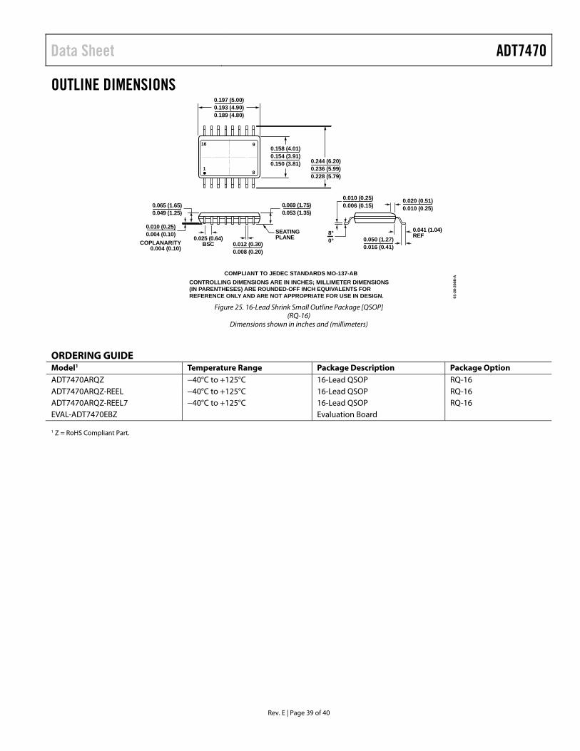
Data Sheet ADT7470
Rev. E | Page 39 of 40
OUTLINE DIMENSIONS
COMPLIANT TO JEDEC STANDARDS MO-137-ABCONTROLLING DIMENSIONS ARE IN INCHES; MILLIMETER DIMENSIONS(IN PARENTHESES) ARE ROUNDED-OFF INCH EQUIVALENTS FORREFERENCE ONLY AND ARE NOT APPROPRIATE FOR USE IN DESIGN.
16 9
81
SEATINGPLANE
0.010 (0.25)0.004 (0.10)
0.012 (0.30)0.008 (0.20)
0.025 (0.64)BSC
0.041 (1.04)REF
0.010 (0.25)0.006 (0.15)
0.050 (1.27)0.016 (0.41)
0.020 (0.51)0.010 (0.25)
8°0°COPLANARITY
0.004 (0.10)
0.065 (1.65)0.049 (1.25)
0.069 (1.75)0.053 (1.35)
0.197 (5.00)0.193 (4.90)0.189 (4.80)
0.158 (4.01)0.154 (3.91)0.150 (3.81) 0.244 (6.20)
0.236 (5.99)0.228 (5.79)
01-2
8-20
08-A
Figure 25. 16-Lead Shrink Small Outline Package [QSOP]
(RQ-16) Dimensions shown in inches and (millimeters)
ORDERING GUIDE Model1 Temperature Range Package Description Package Option ADT7470ARQZ −40°C to +125°C 16-Lead QSOP RQ-16 ADT7470ARQZ-REEL −40°C to +125°C 16-Lead QSOP RQ-16 ADT7470ARQZ-REEL7 −40°C to +125°C 16-Lead QSOP RQ-16 EVAL-ADT7470EBZ Evaluation Board 1 Z = RoHS Compliant Part.

ADT7470 Data Sheet
Rev. E | Page 40 of 40
NOTES
Purchase of licensed I2C components of Analog Devices or one of its sublicensed Associated Companies conveys a license for the purchaser under the Philips I2C Patent Rights to use these components in an I2C system, provided that the system conforms to the I2C Standard Specification as defined by Philips.
©2004–2013 Analog Devices, Inc. All rights reserved. Trademarks and registered trademarks are the property of their respective owners. D04684-0-4/13(E)