teledyne lecroy · summit t24 gen2x4 summit z3-16 and test platform gen3x16 analysis traffic ......
TRANSCRIPT

Teledyne LeCroy
PCI Express 4.0 Technology and Testing Seminar
Speaker Sam Ho +86-18521728160 [email protected]
PROTOCOL SOLUTIONS GROUP
Teledyne LeCroy Confidential
Agenda
PCI Express 4.0 Analysis & Testing
Sam Ho - Teledyne LeCroy
PCI Express 4.0 Protocol Analysis & Test Tools
Sam Ho - Teledyne LeCroy
2
Teledyne LeCroy
PCI Express 4.0 Next Generation
Protocol Analysis and Test Tools
PROTOCOL SOLUTIONS GROUP
Teledyne LeCroy Confidential
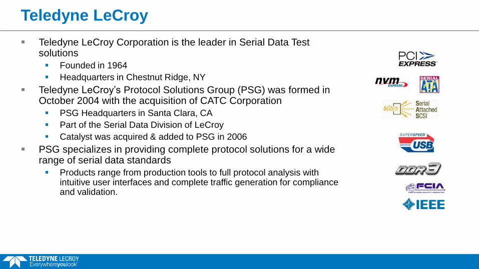
Teledyne LeCroy
Teledyne LeCroy Corporation is the leader in Serial Data Test solutions
Founded in 1964
Headquarters in Chestnut Ridge, NY
Teledyne LeCroy’s Protocol Solutions Group (PSG) was formed in October 2004 with the acquisition of CATC Corporation
PSG Headquarters in Santa Clara, CA
Part of the Serial Data Division of LeCroy
Catalyst was acquired & added to PSG in 2006
PSG specializes in providing complete protocol solutions for a wide range of serial data standards
Products range from production tools to full protocol analysis with intuitive user interfaces and complete traffic generation for compliance and validation.
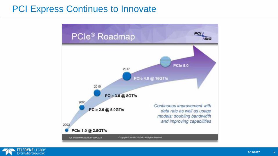
PCI Express Continues to Innovate
9/14/2017 5
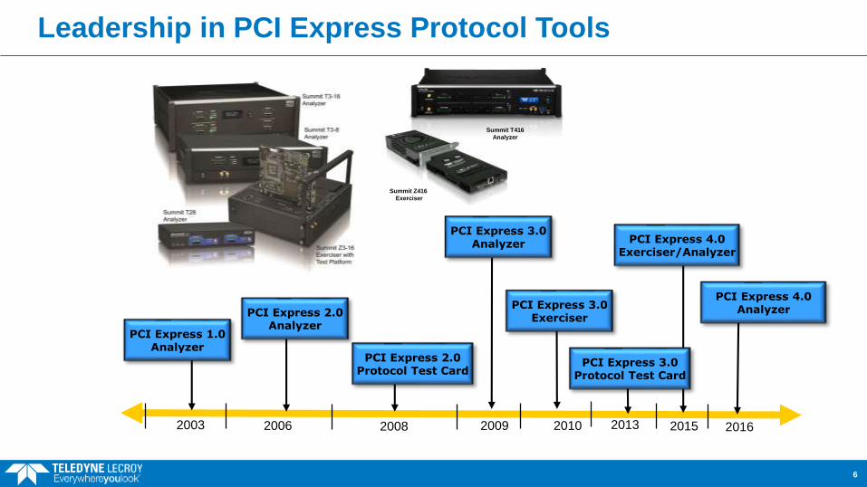
Leadership in PCI Express Protocol Tools
6
2003 2006 2008 2010 20152009
PCI Express 1.0Analyzer
PCI Express 2.0Analyzer
PCI Express 3.0Analyzer
PCI Express 2.0Protocol Test Card
PCI Express 3.0Exerciser
2013
PCI Express 3.0Protocol Test Card
PCI Express 4.0Exerciser/Analyzer
PCI Express 4.0Analyzer
2016
Summit T416
Analyzer
Summit Z416
Exerciser
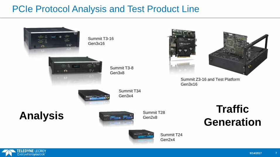
PCIe Protocol Analysis and Test Product Line
9/14/2017 7
Summit T3-16
Gen3x16
Summit T3-8
Gen3x8
Summit T34
Gen3x4
Summit T28
Gen2x8
Summit T24
Gen2x4
Summit Z3-16 and Test Platform
Gen3x16
AnalysisTraffic
Generation
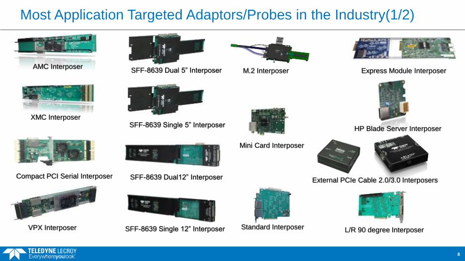
Most Application Targeted Adaptors/Probes in the Industry(1/2)
8
AMC Interposer
XMC Interposer
Compact PCI Serial Interposer
VPX Interposer SFF-8639 Single 12” Interposer
SFF-8639 Dual12” Interposer
SFF-8639 Single 5” Interposer
M.2 InterposerSFF-8639 Dual 5” Interposer
L/R 90 degree Interposer
Mini Card Interposer
Standard Interposer
Express Module Interposer
HP Blade Server Interposer
External PCIe Cable 2.0/3.0 Interposers
M.2 M-Key to x4
PCIe Slot Adapter
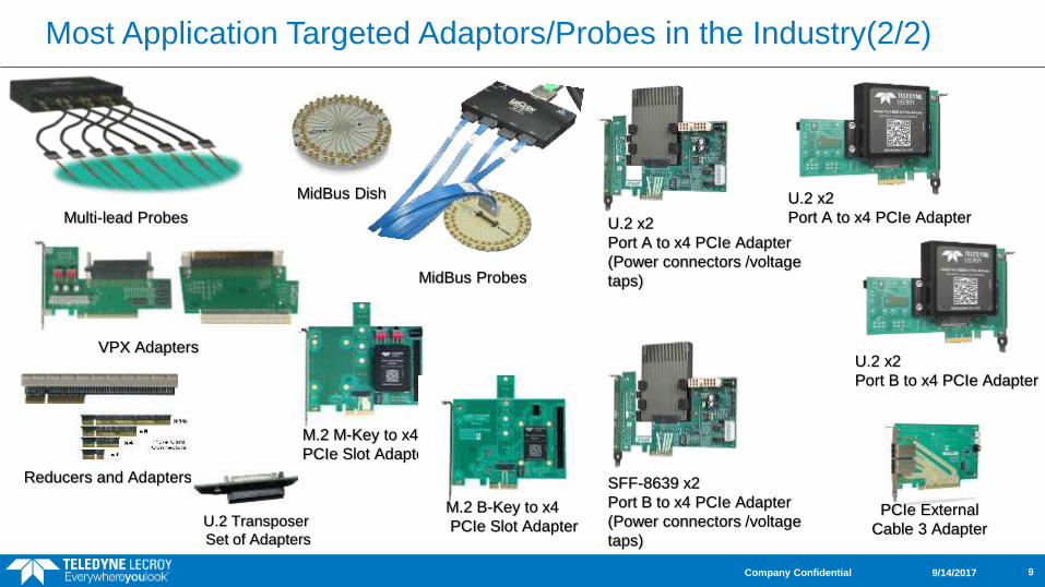
Most Application Targeted Adaptors/Probes in the Industry(2/2)
9/14/2017Company Confidential 9
Multi-lead Probes
MidBus Probes
Reducers and Adapters
M.2 B-Key to x4
PCIe Slot Adapter
U.2 x2
Port A to x4 PCIe Adapter
U.2 x2
Port B to x4 PCIe Adapter
U.2 x2
Port A to x4 PCIe Adapter
(Power connectors /voltage
taps)
SFF-8639 x2
Port B to x4 PCIe Adapter
(Power connectors /voltage
taps)
VPX Adapters
MidBus Dish
U.2 Transposer
Set of Adapters
PCIe External
Cable 3 Adapter
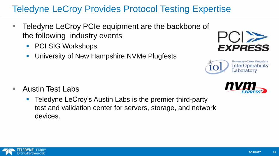
Teledyne LeCroy Provides Protocol Testing Expertise
Teledyne LeCroy PCIe equipment are the backbone of
the following industry events
PCI SIG Workshops
University of New Hampshire NVMe Plugfests
Austin Test Labs
Teledyne LeCroy’s Austin Labs is the premier third-party
test and validation center for servers, storage, and network
devices.
9/14/2017 10

Oscilloscope tools for PCIe 4.0
High-bandwidth signal acquisition
Eye and jitter analysis to 16 Gb/s and beyond
Fixture and channel de-embedding Acquire signals
through Teledyne LeCroy Validation Boards and embed test channel S-parameters in software
PCIe decode from physical to protocol layer
WaveMaster 8Zi-B

Introduction to PCI Express
4.0 and NVMe
What is PCI Express?
PCI Express is a high performance, general purpose I/O interconnect defined for a wide
variety of future computing and communication platforms.
Key PCI attributes, such as its usage model, load-store architecture, and software
interfaces, are maintained, whereas its parallel bus implementation is 5 replaced by a
highly scalable, fully serial interface.
PCI Express takes advantage of recent advances in point-to-point interconnects, Switch-
based technology, and packetized protocol to deliver new levels of performance and
features.
Power Management, Quality Of Service (QoS), Hot-Plug/Hot-Swap support, Data
Integrity, and Error Handling are among some of the advanced features supported by PCI
Express.
The PCI Express Specifications are managed by the PCI Special Interest Group (PCI-
SIG)
13
“PCIe 1.0, 2.0, 3.0, 4.0???”
What is the difference?
These are different revisions of the specification
They do not necessarily mean a device can support higher speeds
The changes go beyond the speed capability and include ECNs and other updates
We tend to use Gen 1, Gen 2, Gen 3 synonymously with 2.5GT/s, 5GT/s and
8GT/s
A PCIe 1.0a or 1.1 device supports 2.5GT/s
A PCIe 2.0 device must support 2.5GT/s and can support 5GT/s
A PCIe 3.0 device must support 2.5GT/s and can support up to 5GT/s and 8GT/s
A PCIe 4.0 device must support 2.5GT/s and can support up to 5GT/s, 8GT/s and 16GT/s
How does this apply to the layered model?
14
“PCIe 1.0, 2.0, 3.0, 4.0???”
The most significant change in specification revisions is to add higher
speed capabilities
PCIe 4.0 supports 16GT/s data rate
Additional capabilities are added in PCIe 4.0
10 bit Tag support
Scaled Flow Control
Lane Margining
Additional retimer support
15
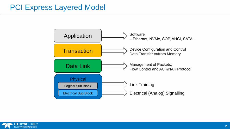
PCI Express Layered Model
Data Link
Transaction
Physical
Application
Logical Sub Block
Electrical Sub Block
Software
– Ethernet, NVMe, SOP, AHCI, SATA…
Device Configuration and Control
Data Transfer to/from Memory
Management of Packets:
Flow Control and ACK/NAK Protocol
Electrical (Analog) Signalling
Link Training
16
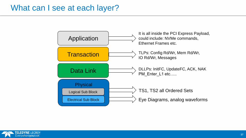
What can I see at each layer?
Data Link
Transaction
Physical
Application
Logical Sub Block
Electrical Sub Block
It is all inside the PCI Express Payload,
could include: NVMe commands,
Ethernet Frames etc.
TLPs: Config Rd/Wr, Mem Rd/Wr,
IO Rd/Wr, Messages
DLLPs: InitFC, UpdateFC, ACK, NAK
PM_Enter_L1 etc…..
Eye Diagrams, analog waveforms
TS1, TS2 all Ordered Sets
17
Physical
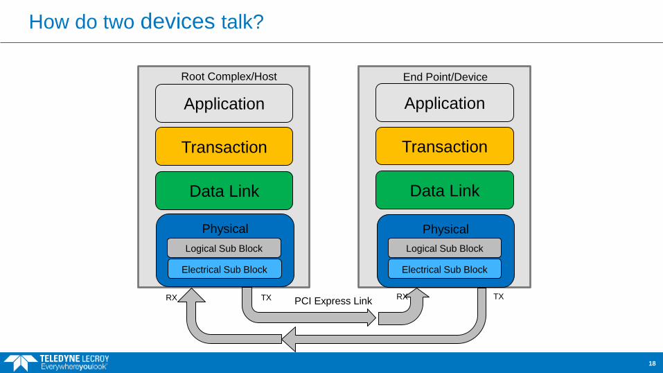
How do two devices talk?
Data LinkData Link
Transaction
Physical
Application Application
Transaction
Logical Sub Block
Electrical Sub Block
Logical Sub Block
Electrical Sub Block
RXRX TX TX
Root Complex/Host End Point/Device
PCI Express Link
18
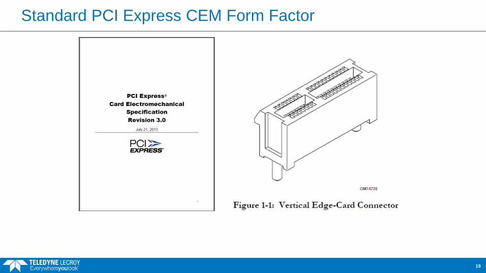
Standard PCI Express CEM Form Factor
19
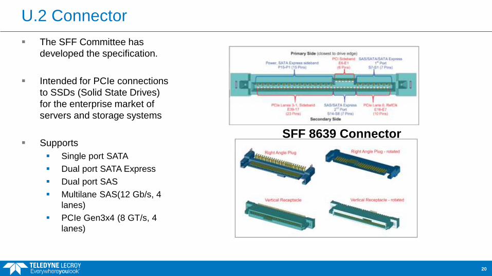
U.2 Connector
The SFF Committee has
developed the specification.
Intended for PCIe connections
to SSDs (Solid State Drives)
for the enterprise market of
servers and storage systems
Supports
Single port SATA
Dual port SATA Express
Dual port SAS
Multilane SAS(12 Gb/s, 4
lanes)
PCIe Gen3x4 (8 GT/s, 4
lanes)
SFF 8639 Connector
20
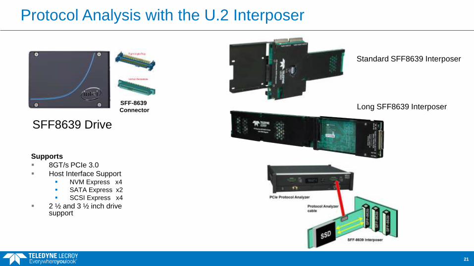
Protocol Analysis with the U.2 Interposer
Supports
8GT/s PCIe 3.0
Host Interface Support NVM Express x4
SATA Express x2
SCSI Express x4
2 ½ and 3 ½ inch drive support
SFF-8639
Connector
SFF8639 Drive
Standard SFF8639 Interposer
Long SFF8639 Interposer
21
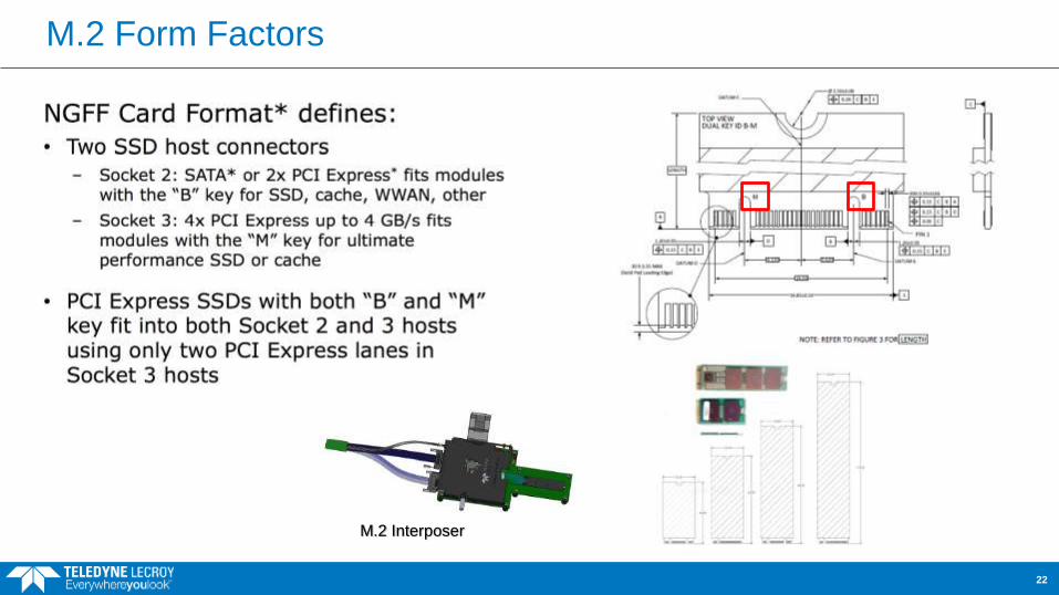
M.2 Form Factors
M.2 Interposer
22
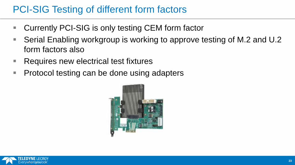
PCI-SIG Testing of different form factors
Currently PCI-SIG is only testing CEM form factor
Serial Enabling workgroup is working to approve testing of M.2 and U.2
form factors also
Requires new electrical test fixtures
Protocol testing can be done using adapters
23
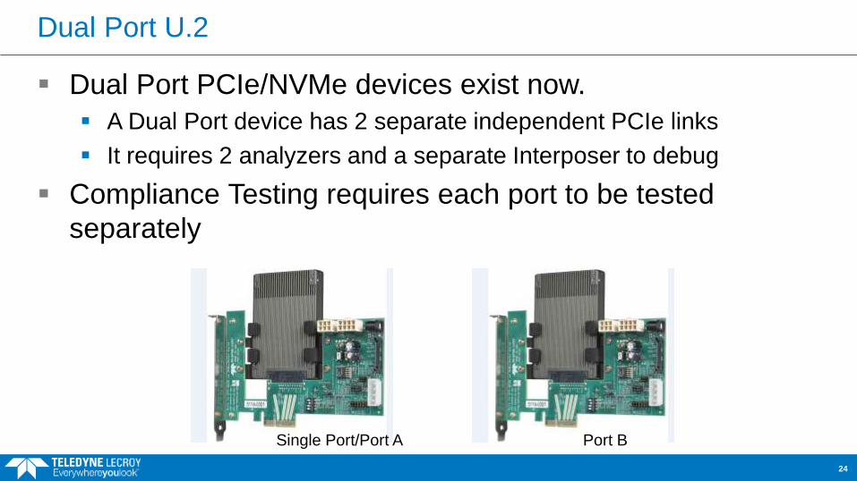
Dual Port U.2
Dual Port PCIe/NVMe devices exist now.
A Dual Port device has 2 separate independent PCIe links
It requires 2 analyzers and a separate Interposer to debug
Compliance Testing requires each port to be tested
separately
24
Single Port/Port A Port B
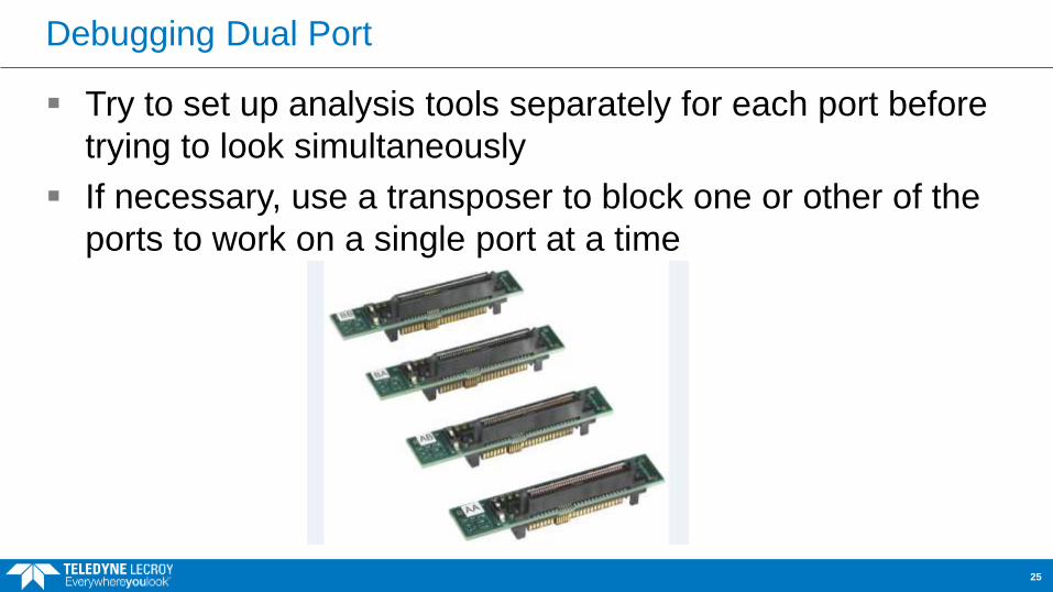
Debugging Dual Port
Try to set up analysis tools separately for each port before
trying to look simultaneously
If necessary, use a transposer to block one or other of the
ports to work on a single port at a time
25
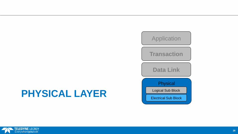
PHYSICAL LAYER
Data Link
Transaction
Physical
Application
Logical Sub Block
Electrical Sub Block
26
PCI Express – Physical Layer
Physical layer is split into 2 blocks:
Electrical
Defines Analog parameters and channel definition
Logical
Defines link training and communication between devices
27
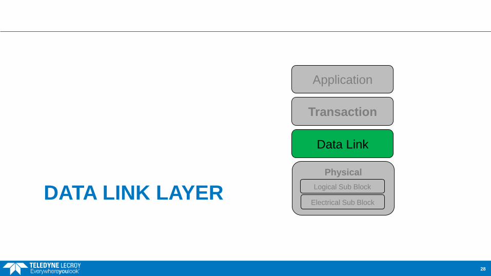
DATA LINK LAYER
Data Link
Transaction
Physical
Application
Logical Sub Block
Electrical Sub Block
28

Data Link Layer
Flow Control Mechanism
TLP Framing (Sequence Numbering)
Error Checking (LCRC)
Handshaking -- Acknowledgement and retry sequences for all TLPs
Two Acknowledgement DLLP packet types:
ACK – acknowledges all TLPs with a Sequence Number less than or equal to AckNak_Seq_Num
NAK – acknowledges all TLPs with a Sequence Number less than or equal to AckNak_Seq_Num and initiates retries of TLPs with a Sequence Number greater than AckNak_Seq_Num.
29
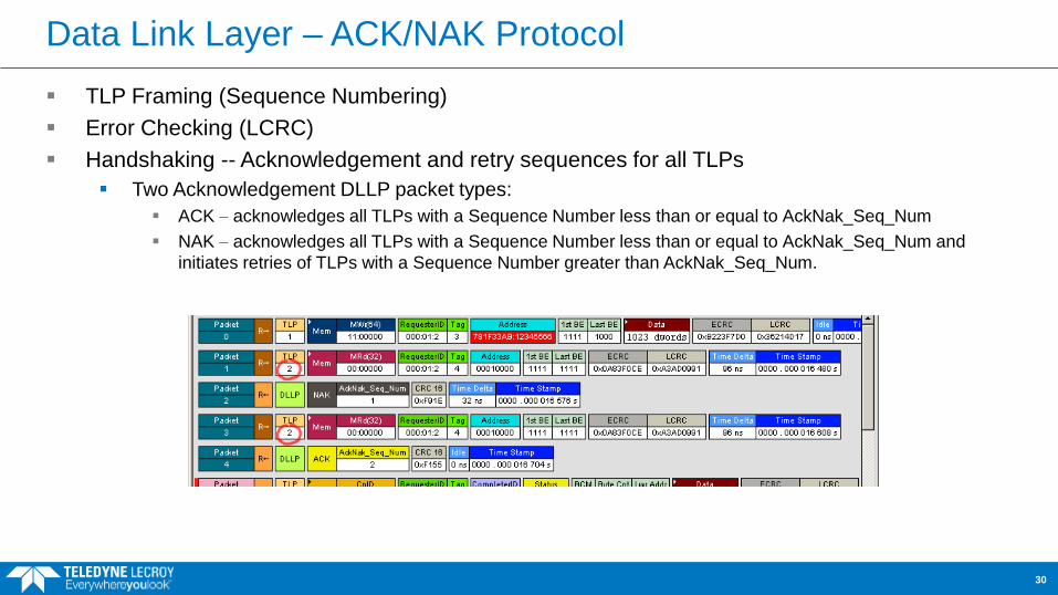
Data Link Layer – ACK/NAK Protocol
TLP Framing (Sequence Numbering)
Error Checking (LCRC)
Handshaking -- Acknowledgement and retry sequences for all TLPs
Two Acknowledgement DLLP packet types:
ACK – acknowledges all TLPs with a Sequence Number less than or equal to AckNak_Seq_Num
NAK – acknowledges all TLPs with a Sequence Number less than or equal to AckNak_Seq_Num and
initiates retries of TLPs with a Sequence Number greater than AckNak_Seq_Num.
30
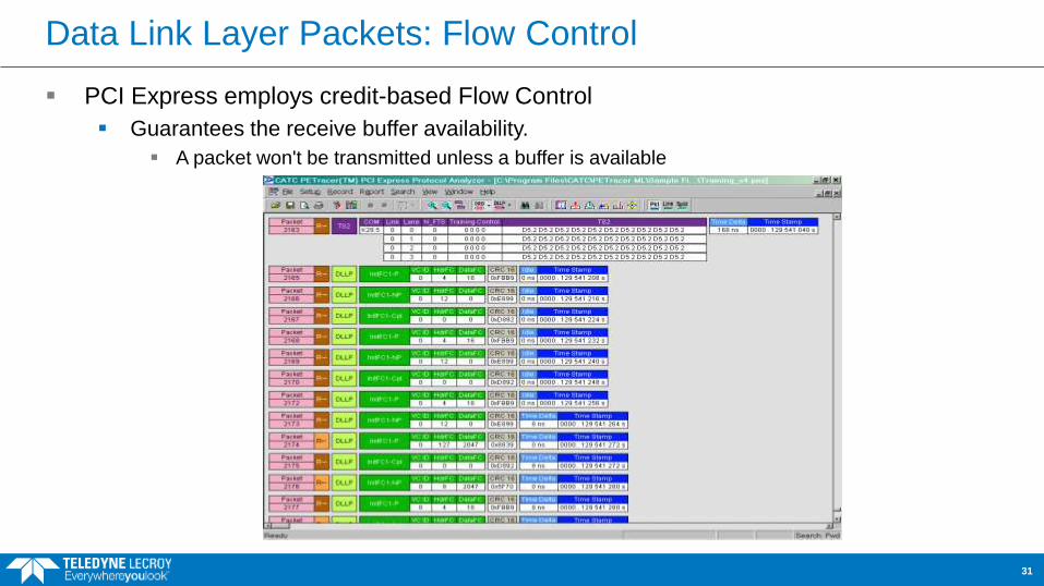
Data Link Layer Packets: Flow Control
PCI Express employs credit-based Flow Control
Guarantees the receive buffer availability.
A packet won't be transmitted unless a buffer is available
31
TRANSACTION
LAYER
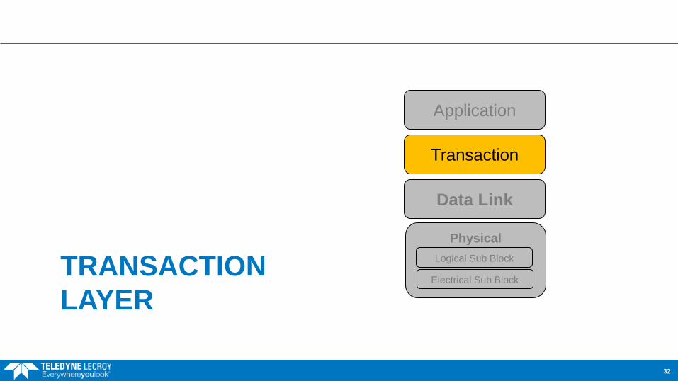
Data Link
Transaction
Physical
Application
Logical Sub Block
Electrical Sub Block
32

Transaction Layer - Transaction Types
Four types of transactions Memory, I/O, Configuration and Message
33
Transaction Layer
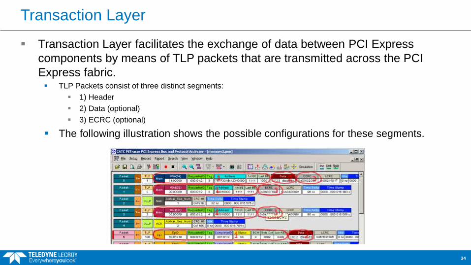
Transaction Layer facilitates the exchange of data between PCI Express
components by means of TLP packets that are transmitted across the PCI
Express fabric. TLP Packets consist of three distinct segments:
1) Header
2) Data (optional)
3) ECRC (optional)
The following illustration shows the possible configurations for these segments.
34
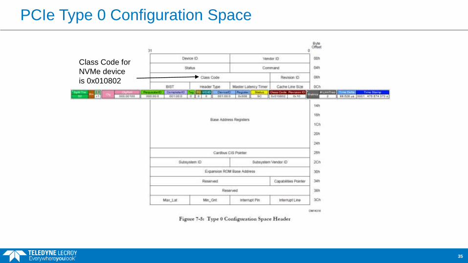
PCIe Type 0 Configuration Space
Class Code for
NVMe device
is 0x010802
35
PCI Express 4.0
PCIe 4.0 New Features
16GT/s Link Speed Capability
Lane Margining
10 bit Tag fields
Scaled Flow Control Credits
37
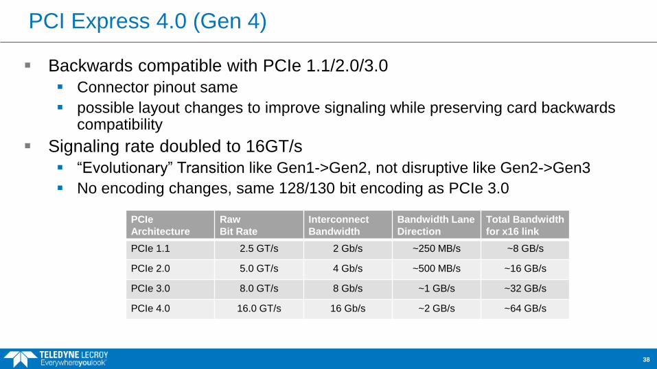
PCI Express 4.0 (Gen 4)
Backwards compatible with PCIe 1.1/2.0/3.0
Connector pinout same
possible layout changes to improve signaling while preserving card backwards compatibility
Signaling rate doubled to 16GT/s
“Evolutionary” Transition like Gen1->Gen2, not disruptive like Gen2->Gen3
No encoding changes, same 128/130 bit encoding as PCIe 3.0
38
PCIe
Architecture
Raw
Bit Rate
Interconnect
Bandwidth
Bandwidth Lane
Direction
Total Bandwidth
for x16 link
PCIe 1.1 2.5 GT/s 2 Gb/s ~250 MB/s ~8 GB/s
PCIe 2.0 5.0 GT/s 4 Gb/s ~500 MB/s ~16 GB/s
PCIe 3.0 8.0 GT/s 8 Gb/s ~1 GB/s ~32 GB/s
PCIe 4.0 16.0 GT/s 16 Gb/s ~2 GB/s ~64 GB/s

16GT/s Equalization Procedure

Equalization Process Part 1 – 2.5GT/s – 8GT/s
Process to change to 16GT/s starts with a speed change to 8GT/s, without
advertising 16GT/S
“The procedure must be executed during the first data rate change to 8.0 GT/s
as well as the first change to all data rates greater than 8.0 GT/s.”
40
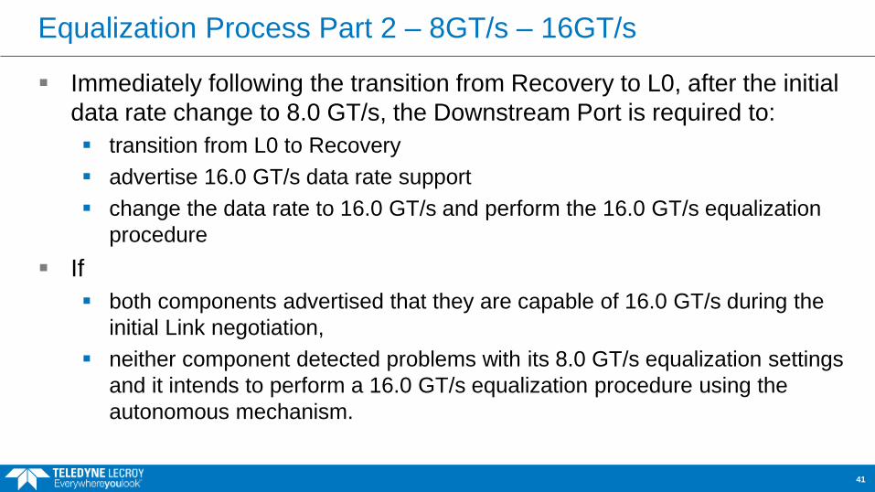
Equalization Process Part 2 – 8GT/s – 16GT/s
Immediately following the transition from Recovery to L0, after the initial
data rate change to 8.0 GT/s, the Downstream Port is required to:
transition from L0 to Recovery
advertise 16.0 GT/s data rate support
change the data rate to 16.0 GT/s and perform the 16.0 GT/s equalization
procedure
If
both components advertised that they are capable of 16.0 GT/s during the
initial Link negotiation,
neither component detected problems with its 8.0 GT/s equalization settings
and it intends to perform a 16.0 GT/s equalization procedure using the
autonomous mechanism.
41

Equalization Process Part 2 – 8GT/s – 16GT/s
Speed Change is initiated to change to speed above 8GT/s
42
TS1 advertises 16.0GT/s Data Rate
Equalization Process
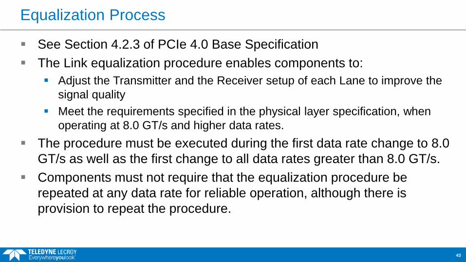
See Section 4.2.3 of PCIe 4.0 Base Specification
The Link equalization procedure enables components to:
Adjust the Transmitter and the Receiver setup of each Lane to improve the
signal quality
Meet the requirements specified in the physical layer specification, when
operating at 8.0 GT/s and higher data rates.
The procedure must be executed during the first data rate change to 8.0
GT/s as well as the first change to all data rates greater than 8.0 GT/s.
Components must not require that the equalization procedure be
repeated at any data rate for reliable operation, although there is
provision to repeat the procedure.
43
Equalization Process
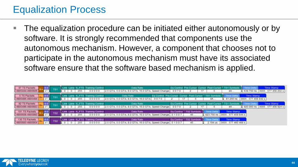
The equalization procedure can be initiated either autonomously or by
software. It is strongly recommended that components use the
autonomous mechanism. However, a component that chooses not to
participate in the autonomous mechanism must have its associated
software ensure that the software based mechanism is applied.
44
16GT/s Equalization Procedure
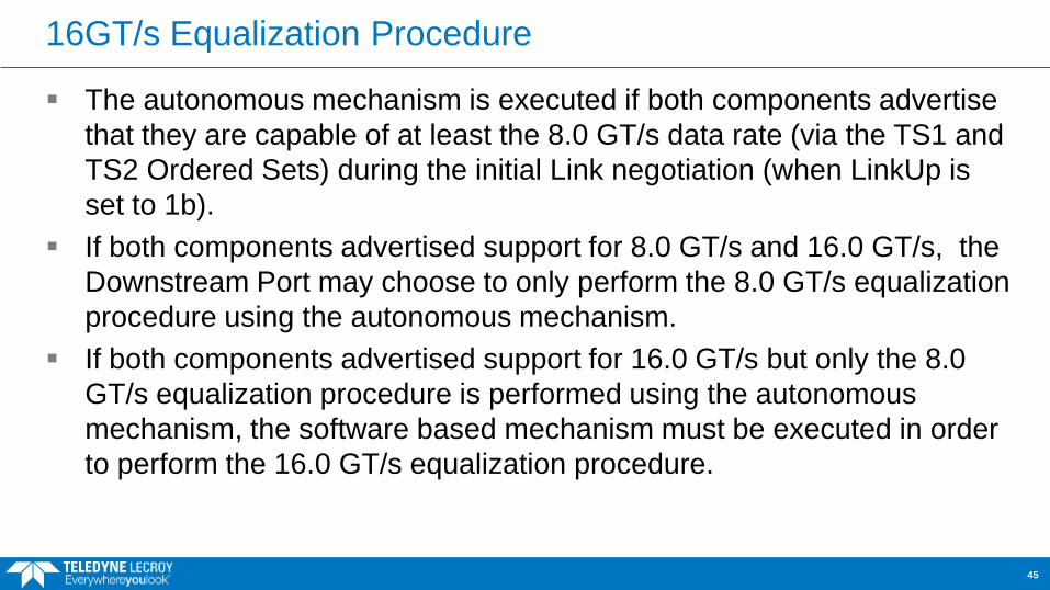
The autonomous mechanism is executed if both components advertise
that they are capable of at least the 8.0 GT/s data rate (via the TS1 and
TS2 Ordered Sets) during the initial Link negotiation (when LinkUp is
set to 1b).
If both components advertised support for 8.0 GT/s and 16.0 GT/s, the
Downstream Port may choose to only perform the 8.0 GT/s equalization
procedure using the autonomous mechanism.
If both components advertised support for 16.0 GT/s but only the 8.0
GT/s equalization procedure is performed using the autonomous
mechanism, the software based mechanism must be executed in order
to perform the 16.0 GT/s equalization procedure.
45
Equalization Procedure
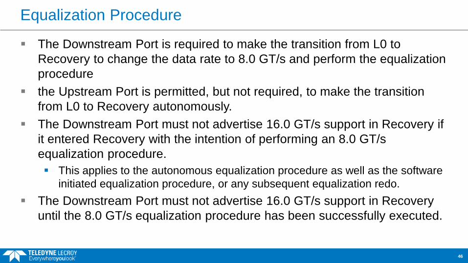
The Downstream Port is required to make the transition from L0 to
Recovery to change the data rate to 8.0 GT/s and perform the equalization
procedure
the Upstream Port is permitted, but not required, to make the transition
from L0 to Recovery autonomously.
The Downstream Port must not advertise 16.0 GT/s support in Recovery if
it entered Recovery with the intention of performing an 8.0 GT/s
equalization procedure.
This applies to the autonomous equalization procedure as well as the software
initiated equalization procedure, or any subsequent equalization redo.
The Downstream Port must not advertise 16.0 GT/s support in Recovery
until the 8.0 GT/s equalization procedure has been successfully executed.
46
Lane Margining at Receiver
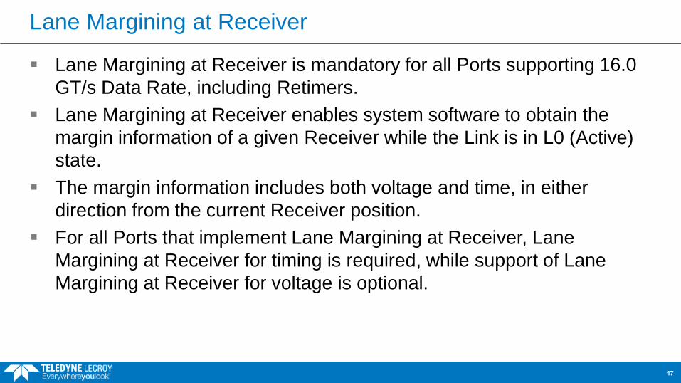
Lane Margining at Receiver is mandatory for all Ports supporting 16.0
GT/s Data Rate, including Retimers.
Lane Margining at Receiver enables system software to obtain the
margin information of a given Receiver while the Link is in L0 (Active)
state.
The margin information includes both voltage and time, in either
direction from the current Receiver position.
For all Ports that implement Lane Margining at Receiver, Lane
Margining at Receiver for timing is required, while support of Lane
Margining at Receiver for voltage is optional.
47

Lane Margining at Receiver
Software mechanism to “step” through different sampling points in the
receiver
Hardware reports errors, not a hardware mechanism like the
Recovery.Equalization state.
48
Expanded Tag Fields
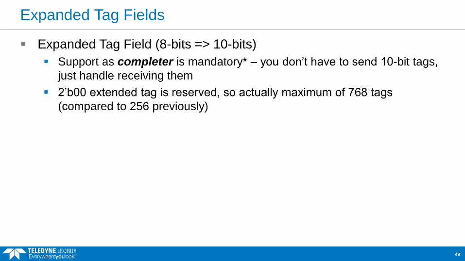
Expanded Tag Field (8-bits => 10-bits)
Support as completer is mandatory* – you don’t have to send 10-bit tags,
just handle receiving them
2’b00 extended tag is reserved, so actually maximum of 768 tags
(compared to 256 previously)
49

Scaled Flow Control
Link performance can be affected when there are insufficient flow
control credits available to account for the Link round trip time. This
effect becomes more noticeable at higher Link speeds and the limitation
of 127 header credits and 2047 data credits can limit performance. The
Scaled Flow Control mechanism is designed to address this limitation.
50
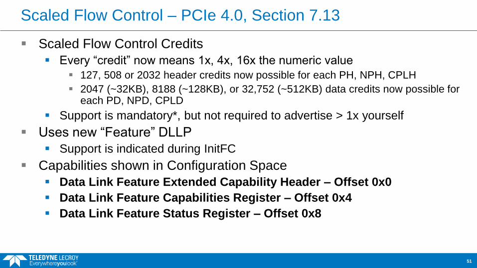
Scaled Flow Control – PCIe 4.0, Section 7.13
Scaled Flow Control Credits
Every “credit” now means 1x, 4x, 16x the numeric value
127, 508 or 2032 header credits now possible for each PH, NPH, CPLH
2047 (~32KB), 8188 (~128KB), or 32,752 (~512KB) data credits now possible for each PD, NPD, CPLD
Support is mandatory*, but not required to advertise > 1x yourself
Uses new “Feature” DLLP
Support is indicated during InitFC
Capabilities shown in Configuration Space
Data Link Feature Extended Capability Header – Offset 0x0
Data Link Feature Capabilities Register – Offset 0x4
Data Link Feature Status Register – Offset 0x8
51
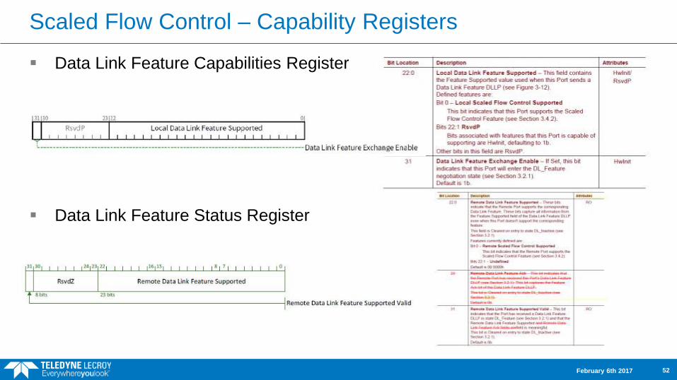
Scaled Flow Control – Capability Registers
Data Link Feature Capabilities Register
February 6th 2017 52
Data Link Feature Status Register
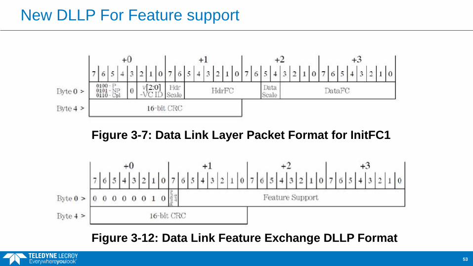
New DLLP For Feature support
53
Figure 3-7: Data Link Layer Packet Format for InitFC1
Figure 3-12: Data Link Feature Exchange DLLP Format
References
PCI Express Base Specification v3.1
PCI Express CEM Specification v.3.0
PCI Express Base Specification v4.0 (Draft 0.91, August 2017)
54
PCI Express 4.0
Compliance Testing
February 6th 2017 55
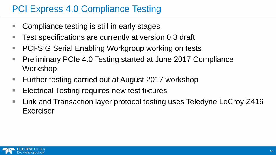
PCI Express 4.0 Compliance Testing
Compliance testing is still in early stages
Test specifications are currently at version 0.3 draft
PCI-SIG Serial Enabling Workgroup working on tests
Preliminary PCIe 4.0 Testing started at June 2017 Compliance
Workshop
Further testing carried out at August 2017 workshop
Electrical Testing requires new test fixtures
Link and Transaction layer protocol testing uses Teledyne LeCroy Z416
Exerciser
56
PCI Express 4.0
Test Tools
February 6th 2017 57

Test Board/Adapters for Gen 4 Electrical Performance Testing
Two different Gen 4 test Fixtures offered: Gen 4 Verification Load Board (TL-VLB)
Gen 4 Verification Base Board (TL-VBB)
Both support up to x16 configurations
Differ from “Compliance Test Boards” PCI_SIG's Compliance Load Board (CLB) and
Compliance Base Board (CBB) are optimized for compliance testing. These boards add trace loss on purpose to work
in conjunction with jitter induced eye closure from a Bit Error Rate Test tool to mimic more realistic customer channels.
The TL-VLB and TL-VBB test fixtures are optimized for measuring the inherent electrical performance of your system and/or device such as TX Jitter and signal amplitude.
58

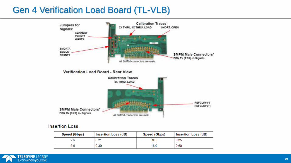
Gen 4 Verification Load Board (TL-VLB)
Gen 4 Load Board Adapter: Supports up to a x16 link width
Intended for electrical performance testing of platform systems
Inserts into a standard CEM connector as the Device while allowing access to the devices TX and RX signaling through high speed RF connectors.
Allows insertion or reception of electrical signals to/from the Motherboard under test.
Optimized for minimal channel loss with 16GT/s signaling in mind. By optimizing the PCB material, stackup, and trace
geometries, this adapter facilitates more accurate measurements of your devices electrical performance.
59
Gen 4 Verification Load Board (TL-VLB)
60
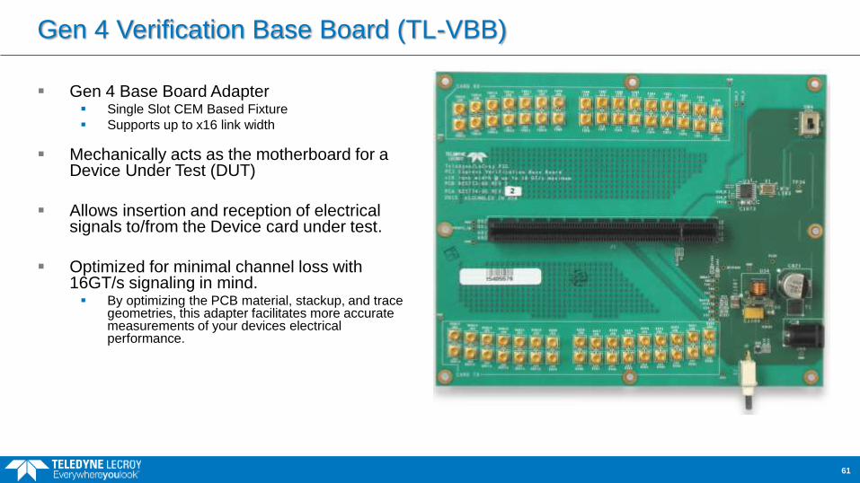
Gen 4 Verification Base Board (TL-VBB)
Gen 4 Base Board Adapter Single Slot CEM Based Fixture
Supports up to x16 link width
Mechanically acts as the motherboard for a Device Under Test (DUT)
Allows insertion and reception of electrical signals to/from the Device card under test.
Optimized for minimal channel loss with 16GT/s signaling in mind. By optimizing the PCB material, stackup, and trace
geometries, this adapter facilitates more accurate measurements of your devices electrical performance.
61
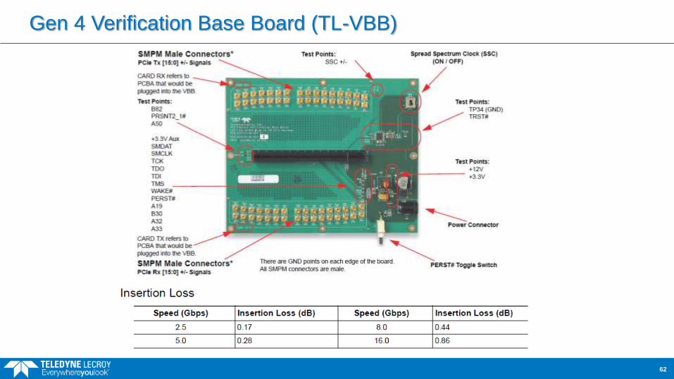
Gen 4 Verification Base Board (TL-VBB)
62
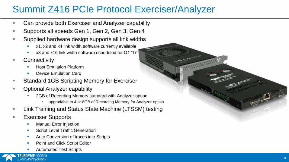
Summit Z416 PCIe Protocol Exerciser/Analyzer
Can provide both Exerciser and Analyzer capability
Supports all speeds Gen 1, Gen 2, Gen 3, Gen 4
Supplied hardware design supports all link widths
x1, x2 and x4 link width software currently available
x8 and x16 link width software scheduled for Q1 ‘17
Connectivity
Host Emulation Platform
Device Emulation Card
Standard 1GB Scripting Memory for Exerciser
Optional Analyzer capability
2GB of Recording Memory standard with Analyzer option
upgradable to 4 or 8GB of Recording Memory for Analyzer option
Link Training and Status State Machine (LTSSM) testing
Exerciser Supports
Manual Error Injection
Script Level Traffic Generation
Auto Conversion of traces into Scripts
Point and Click Script Editor
Automated Test Scripts
8
Summit Z416 - Product Form Factor (1 of 2)
64
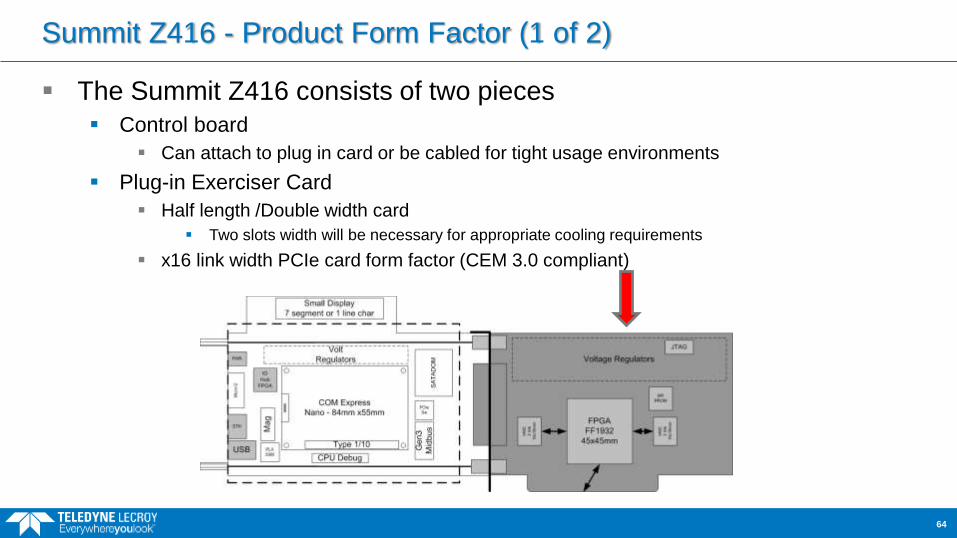
The Summit Z416 consists of two pieces
Control board
Can attach to plug in card or be cabled for tight usage environments
Plug-in Exerciser Card
Half length /Double width card
Two slots width will be necessary for appropriate cooling requirements
x16 link width PCIe card form factor (CEM 3.0 compliant)
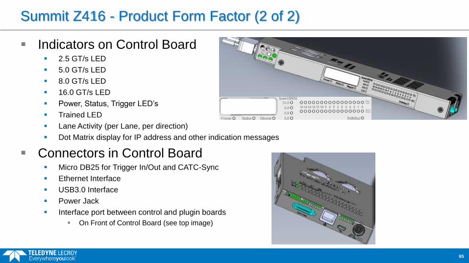
Summit Z416 - Product Form Factor (2 of 2)
65
Indicators on Control Board 2.5 GT/s LED
5.0 GT/s LED
8.0 GT/s LED
16.0 GT/s LED
Power, Status, Trigger LED’s
Trained LED
Lane Activity (per Lane, per direction)
Dot Matrix display for IP address and other indication messages
Connectors in Control Board Micro DB25 for Trigger In/Out and CATC-Sync
Ethernet Interface
USB3.0 Interface
Power Jack
Interface port between control and plugin boards
On Front of Control Board (see top image)
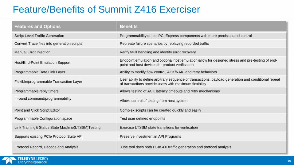
Feature/Benefits of Summit Z416 Exerciser
Features and Options Benefits
Script Level Traffic Generation Programmability to test PCI Express components with more precision and control
Convert Trace files into generation scripts Recreate failure scenarios by replaying recorded traffic
Manual Error Injection Verify fault handling and identify error recovery
Host/End-Point Emulation SupportEndpoint emulation(and optional host emulation)allow for designed stress and pre-testing of end-
point and host devices for product verification
Programmable Data Link Layer Ability to modify flow control, ACK/NAK, and retry behaviors
Flexible/programmable Transaction LayerUser ability to define arbitrary sequence of transactions, payload generation and conditional repeat
of transactions provide users with maximum flexibility
Programmable reply timers Allows testing of ACK latency timeouts and retry mechanisms
In-band command/programmability Allows control of testing from host system
Point and Click Script Editor Complex scripts can be created quickly and easily
Programmable Configuration space Test user defined endpoints
Link Training& Status State Machine(LTSSM)Testing Exercise LTSSM state transitions for verification
Supports existing PCIe Protocol Suite API Preserve investment in API Programs
Protocol Record, Decode and Analysis One tool does both PCIe 4.0 traffic generation and protocol analysis
66

Summit Z416 Exerciser Additional Capabilities/Options/Functions
Summit Z416 Exerciser is being designed to support the following additional
capabilities/options/functions:
Programmable LTSSM
Automated or fully scripted LTSSM
Enhanced error injection
Error injection by lane
On-board Analyzer/Analysis Capabilities
No need for a “standalone analyzer” when using the Z416 exerciser
Ability to run all PCIe, NVMe and NVMe-MI compliance
In-band command/programmability
67
Summit Z416 capabilities roll-out
68
Currently available capabilities: Utilizes PCIe Protocol Suite V8.xx software
Can provide both Exerciser and Analyzer capability
Supports all speeds Gen 1, Gen 2, Gen 3, Gen 4
Support for x1 and x4 link widths
Supports Standard, SRIS or External clocking
Supports CLKREQ# for low power modes
Focused on LTSSM structures and bring up Target Link-UP to L0 state (will maintain L0 state)
Provides automatic skip generation
Will ACK packets received
Supports lane reversal
Can control polarity and scrambling
Handles Autonomous Speed Switch
Error Injection for Training Sequences (per lane)
Will support all current software views and capabilities
Analyzer will capture all bus traffic Snapshot mode
ordered set and LTSSM state change triggers to analyzer
Future capabilities: Supports all link widths – up to x16
Support for SMBus traffic generation
Emulate either root complex or end-point Auto respond to Read/Write to configuration space
Error injection into Ordered Sets, DLLP’s, TLP’s Per packet or by lane
Full Scripting Ability Supports Gen 3 Compliance Scripts
Supports NVMe Compliance Scripts
Supports NVMe-MI Compliance Scripts
Supports and adheres to Flow Control Includes InitFC and UpdateFC
posted, non-posted, completion header and completion data
Will Auto-Generate Sequence Numbers
Both 5 and 8 bit tags
CRC’s
Full Control of ACK/NAK policies Supports Auto-Replay and Link Recovery
Provides Read/Write for all I/O buffers
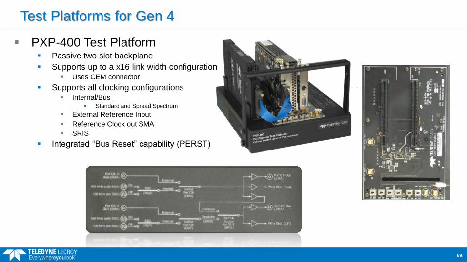
Test Platforms for Gen 4
PXP-400 Test Platform Passive two slot backplane
Supports up to a x16 link width configuration Uses CEM connector
Supports all clocking configurations Internal/Bus
Standard and Spread Spectrum
External Reference Input
Reference Clock out SMA
SRIS
Integrated “Bus Reset” capability (PERST)
69

PXP400 Test Platform for Gen 4
70
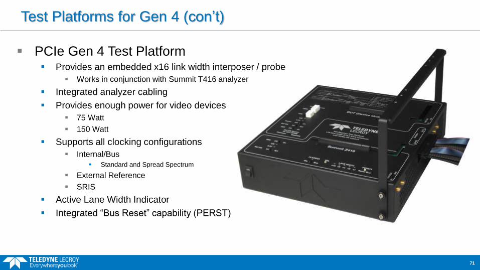
Test Platforms for Gen 4 (con’t)
71
PCIe Gen 4 Test Platform Provides an embedded x16 link width interposer / probe
Works in conjunction with Summit T416 analyzer
Integrated analyzer cabling
Provides enough power for video devices
75 Watt
150 Watt
Supports all clocking configurations
Internal/Bus
Standard and Spread Spectrum
External Reference
SRIS
Active Lane Width Indicator
Integrated “Bus Reset” capability (PERST)

PCIe Gen 4 Test Platform Detail
72
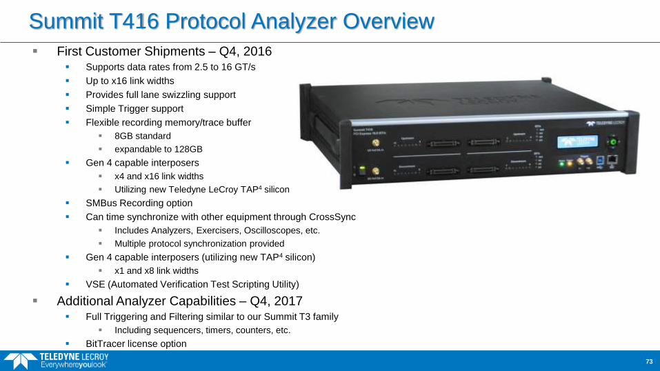
Summit T416 Protocol Analyzer Overview
First Customer Shipments – Q4, 2016 Supports data rates from 2.5 to 16 GT/s
Up to x16 link widths
Provides full lane swizzling support
Simple Trigger support
Flexible recording memory/trace buffer
8GB standard
expandable to 128GB
Gen 4 capable interposers
x4 and x16 link widths
Utilizing new Teledyne LeCroy TAP4 silicon
SMBus Recording option
Can time synchronize with other equipment through CrossSync
Includes Analyzers, Exercisers, Oscilloscopes, etc.
Multiple protocol synchronization provided
Gen 4 capable interposers (utilizing new TAP4 silicon)
x1 and x8 link widths
VSE (Automated Verification Test Scripting Utility)
Additional Analyzer Capabilities – Q4, 2017 Full Triggering and Filtering similar to our Summit T3 family
Including sequencers, timers, counters, etc.
BitTracer license option
73

Summit T416 has the Broadest Range of Protocol Decodes
Standard Protocol Decodes include: PCIe (PCI-Express)
Packet Layer
Link Layer
Split Transaction Layer
NVMe (Non-Volatile Memory Express)
Transaction Layer
Command Layer
ATS (Address Translation Services)
PTM (Precision Time Management)
Virtualization protocols including: SRIOV (Single Root I/O Virtualization)
MRIOV (Multi-Root I/O Virtualization)
SATA-Express including: AHCI (Advanced Host Controller Interface)
ATA (AT Advanced)
SCSI-Express including: PQI (PCIe Queuing Interface)
SOP (SCSI Operating Protocol)
SCSI (Small Computer System Interface)
74
Additional Optional Protocols include:
TCG (Trusted Computer Group)
Enterprise
Opal
MCTP (Management Component Transport Protocol)
PLDM (Platform Level Data Model)
NC-SI (Network Controller Sideband Interface)
NVMe-MI (NVMe Management Interface)
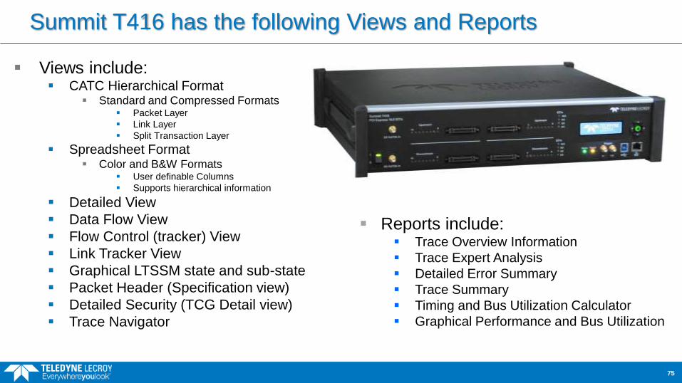
Summit T416 has the following Views and Reports
Views include: CATC Hierarchical Format
Standard and Compressed Formats Packet Layer
Link Layer
Split Transaction Layer
Spreadsheet Format Color and B&W Formats
User definable Columns
Supports hierarchical information
Detailed View
Data Flow View
Flow Control (tracker) View
Link Tracker View
Graphical LTSSM state and sub-state
Packet Header (Specification view)
Detailed Security (TCG Detail view)
Trace Navigator
75
Reports include: Trace Overview Information
Trace Expert Analysis
Detailed Error Summary
Trace Summary
Timing and Bus Utilization Calculator
Graphical Performance and Bus Utilization
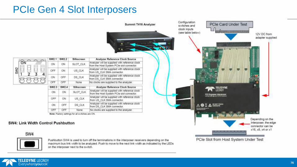
PCIe Gen 4 Slot Interposers
76
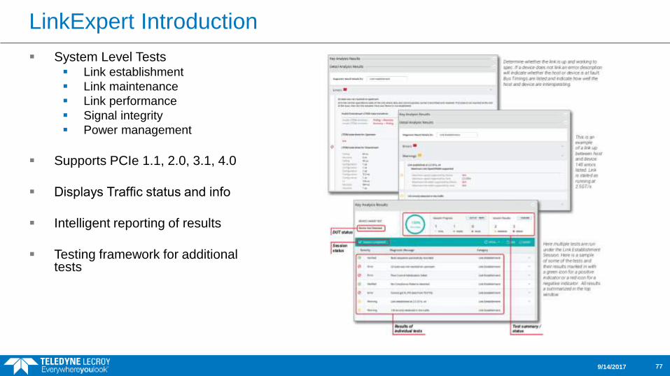
LinkExpert Introduction
System Level Tests Link establishment
Link maintenance
Link performance
Signal integrity
Power management
Supports PCIe 1.1, 2.0, 3.1, 4.0
Displays Traffic status and info
Intelligent reporting of results
Testing framework for additional tests
9/14/2017 77
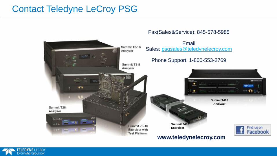
Contact Teledyne LeCroy PSG
Fax(Sales&Service): 845-578-5985
Email Sales: [email protected]
Phone Support: 1-800-553-2769
www.teledynelecroy.com
Summit Z416
Exerciser
SummitT416
Analyzer

Thank You!