taking advantage of lvds input buffers to implement sigma ...erives/531_14/sigma-delta.pdf ·...
TRANSCRIPT
TAKING ADVANTAGE OF LVDS INPUT BUFFERS
TO IMPLEMENT SIGMA-DELTA A/D CONVERTERS IN FPGAS
Fabio Sousa1, Volker Mauer
1, Neimar Duarte
2, Ricardo P. Jasinski
3, Volnei A. Pedroni
3
1 Altera Europe, High Wycombe, United Kingdom 2 PI Componentes / Altera, São Paulo, Brazil
3 Federal Center of Technological Education of Parana – CEFET/PR, Curitiba-PR, Brazil
ABSTRACT
This paper describes the implementation of a sigma-delta
( ) A/D converter within an FPGA, with minimal use of
external analog components. The approach takes
advantage of existing low-voltage differential signaling
(LVDS) I/O pads; this allows the implementation of low-
cost ADCs into existent FPGAs, even though such digital
devices do not posses analog interfacing capabilities at
first. The converter was implemented in an actual FPGA
and had its performance evaluated.
1. INTRODUCTION
Programmable Logic Devices (FPGAs included) are well-
known for their ability to implement digital logic and
interface with other digital circuits. However, PLD
manufacturers traditionally do not integrate analog
interfaces in their devices, and all interface between PLDs
and analog signals must be done by means of A/D and
D/A converters.
The implementation of ADCs on such digital
chips is desirable for several reasons, including cost,
board space and reduced number of components.
However, traditional I/O pads found in PLDs do not allow
the implementation of any ADC architecture.
Now, with the most recent FPGA families
supporting the Low-Voltage Differential Signaling
(LVDS) standard, the implementation of ADCs in a PLD
becomes feasible.
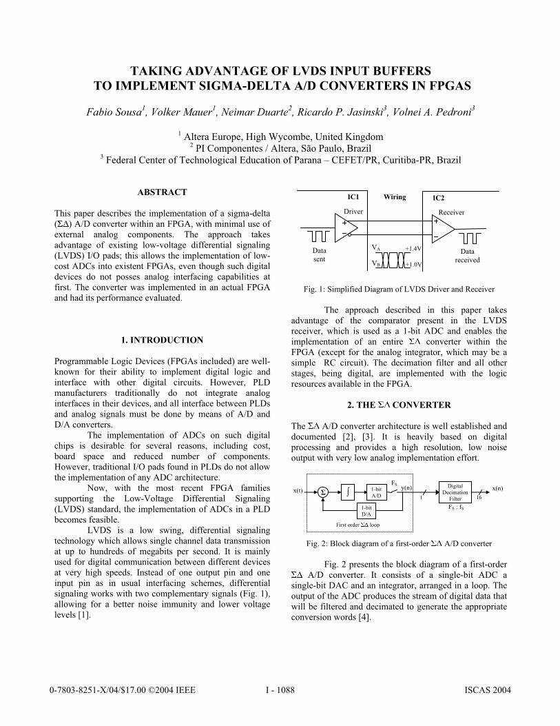
LVDS is a low swing, differential signaling
technology which allows single channel data transmission
at up to hundreds of megabits per second. It is mainly
used for digital communication between different devices
at very high speeds. Instead of one output pin and one
input pin as in usual interfacing schemes, differential
signaling works with two complementary signals (Fig. 1),
allowing for a better noise immunity and lower voltage
levels [1].
Fig. 1: Simplified Diagram of LVDS Driver and Receiver
The approach described in this paper takes
advantage of the comparator present in the LVDS
receiver, which is used as a 1-bit ADC and enables the
implementation of an entire converter within the
FPGA (except for the analog integrator, which may be a
simple RC circuit). The decimation filter and all other
stages, being digital, are implemented with the logic
resources available in the FPGA.
2. THE CONVERTER
The A/D converter architecture is well established and
documented [2], [3]. It is heavily based on digital
processing and provides a high resolution, low noise
output with very low analog implementation effort.
Fig. 2: Block diagram of a first-order A/D converter
Fig. 2 presents the block diagram of a first-order
A/D converter. It consists of a single-bit ADC a
single-bit DAC and an integrator, arranged in a loop. The
output of the ADC produces the stream of digital data that
will be filtered and decimated to generate the appropriate
conversion words [4].
Driver Receiver
Wiring IC2IC1
Data
sentData
received
VA
VB
+1.4V
+1.0V
x(t) 1-bit
A/D
Digital
Decimation
Filter
1-bit
D/A
First order loop
FS
FS : fS
y(n)
1 16
x(n)

The architecture has been chosen because of its highly
digital characteristics, beneficial for FPGA implementation
since it allows maximum integration within the device [5].
A higher effective resolution can be achieved with the use
of a higher-order modulation filter, which will be the
object of further studies.
The implemented converter is shown in Fig. 3.
As can be seen, it uses 3 FPGA pins: 2 LVDS pins for the
analog signals, and one conventional I/O pin which feeds
the integrator. The analog input is applied to the
comparator positive input, and is constantly compared
against the integrated signal. In this way, the only external
components to the FPGA are the resistor and capacitor,
which compose the integrator.
The LVDS comparator is used as a 1-bit ADC,
the output of which is sampled at the oversampling rate.
The registered output forms the bitstream that will be fed
to both the integrator and the digital filtering and
decimation stages. A conventional output pin works as the
1-bit DAC, providing the input signal to the integrator.
This approach makes possible the implementation of very
low cost A/D converters into existing FPGAs, even
though such devices do not possess analog interfaces at
first.
The prototype converter was designed to operate
in the audio range (up to 20 kHz). The values chosen for R
and C were 1k and 1nF, providing a pole 3 octaves
above the highest frequency in the band of interest.
The circuit operates from a 50MHz clock source,
sampling the comparator output and producing the
bitstream to the decimation stage at this same rate. The
filter and decimation stages provide a downsampling of
1024 (OSR), presenting output samples at 48.8 kHz.
Details of the filtering and decimation stage are
shown in Fig. 4. It comprises: (a) a Cascaded Integrator-
Comb (CIC) filter, which reduces the input sampling rate
[6]; (b) an equalizer, which compensates for the
magnitude drooping introduced by the first stage and
performs a low rate change, and (c) a low-pass filter,
which exhibits a sharp cutoff frequency limiting the
output to the band of interest.
The CIC stage receives 1-bit samples at 50MHz,
Fig. 4: Implementation of the filtering and decimation stages
1 Comb
Filter (CIC)
Inside FPGA Outside FPGA
LVDS+ pin
LVDS- pin
Analog input
Regular
I/O pin
LVDS Receiver
(1-bit ADC)
R
C
Integrator
D Q
clock
Converted
signal
12-bit
48.8 kHz
1
50 MHz
12
97.6 kHz
12
48.8 kHz
Decimation
Factor = 512
Decimation
Factor = 2 No
Decimation
2 Equalizer
(FIR Filter)
3 LPF
(FIR Filter)
Filtering and Decimation
Fig. 3: Block diagram of the implemented A/D converter
(1-bit DAC)

and outputs 12-bit samples at 97.656 kHz. It consists of a
2-stage CIC filter with a rate change factor of 512.
The equalizer stage receives the output samples
from the preceding CIC filter, and outputs 12-bit samples
at 48.828 kHz. It consists of a 21-coefficient FIR filter,
with its frequency response designed to compensate for
the magnitude attenuation of the preceding stage. It also
provides an additional decimation factor of 2.
The low-pass filter stage is designed to attenuate
signals outside the band of interest, with a very sharp
cutoff frequency at 20 kHz. It consists of a 63-coefficient
FIR filter, and outputs 12-bit samples at 48.828 kHz (no
decimation is performed in this stage).
All filtering and decimation stages were
implemented in hardware using the logic resources
available within the FPGA.
3. SIMULATION RESULTS
Since the on-chip comparators were not originally
intended for this kind of use, a series of simulations were
performed using the SPICE model of the comparator
found in actual FPGAs. The model was provided by
Altera, and is currently implemented in all EP1S and
EP1C devices.
Simulations have been realized to evaluate the
comparator’s performance over the desired input voltage
range (0 to 3.3V), since the LVDS standard operates
typically from 1.0 to 1.4 V. It has been verified that the
comparator exhibits good performance over the whole
input range from 0 to 3.3V, which encouraged the
physical implementation of the converter. Fig. 5 shows the
results for some of these simulations. The upper plot
shows functional verifications and offset measurements,
while the second plot shows hysteresis measurements
(<30 mV).
Fig. 5: Spice simulation results for the on-chip comparator
Another HSPICE simulation is shown in Fig. 6,
this time including the register and the integrator circuit.
The objective was to record the sampled input signal, and
later compare it to the output of a known modulator,
the model of which was available in Matlab. From the
results of both simulations it was concluded that the
intended modulator architecture performed as expected,
which further motivated the implementation of the
converter.
Fig. 6: Simulations results for the modulator
4. EXPERIMENTAL RESULTS
Having the simulation results indicated the feasibility of
the architecture, the entire converter was physically
implemented in an actual FPGA (Altera EP1S25
F672C6ES), requiring around 700 logic elements. A
standard development board (Fig. 7) was used in the
experiments, without additional shielding or noise-
reducing mechanisms, so even better results would be
expected in a more adequate environment.
Fig. 7: Development board used in the experiments
Also, the choice of a first-order modulator for the
ADC is a major performance limiting factor; there is a
heavy trade-off between performance and integration. It
C = 1 nF
R = 1 k
-10mV
+10mV
Matlab – 20 kHz sinewave + Theoretical Modulator
HSPICE – 20 kHz sinewave + LVDS Modulator
Comparator (V+)
Comparator (V-)

was not intended, in this specific implementation, to
achieve the full resolution of available off-the-shelf A/D
converters, but rather demonstrate the feasibility of this
novel approach.
In order to verify the functionality and
performance of the implemented converter, its SNR curve
has been characterized. For input signals from 100 Hz to
20 kHz, the SNR was measured as follows:
A sinusoidal analog signal of a given frequency, with a
voltage swing of 3.3V, was generated and applied to the
input of the converter;
A series of 49,152 samples from the output of the
converter were recorded inside the FPGA;
The collected data was transmitted to a PC and had its
FFT computed (Fig. 8 presents the results for an input
signal of 15 kHz);
From the FFT points, the signal-to-noise relation was
computed, considering as noise all frequencies but the
one of the original input signal.
Fig. 8: FFT of the converted signal for a sinusoidal
input of 15 kHz
Fig. 9 presents the measured SNR distribution
from 100 Hz to 20 kHz. The best value was found at 15
kHz, with a SNR of 61.2 dB and an effective number of
bits of 9.87.
Fig. 9: Measured SNR distribution for the implemented
converter
5. CONCLUSION AND FUTURE WORK
The implementation of a A/D converter in an
originally fully digital domain (FPGA) with minimal
external components required (a simple RC circuit) has
been demonstrated. The experimental results proved the
feasibility of the proposed solution.
Further studies comprise a more complete
characterization of the on-chip comparator, in order to
determine its time response and offset voltage over the
entire input range; the implementation of higher-order
modulators, in order to pursue a higher resolution (number
of effective bits), and the implementation of converters
with higher oversampling rates (OSR). It is expected that
A/D converters with resolution of 10-12 bits or more can
be achieved with this technique.
6. REFERENCES
[1] National Semiconductor, “LVDS Owner’s Manual”, 2000.
[2] M. Rebeschini et al, “A High-Resolution CMOS Sigma-Delta
A/D Converter with 320 kHz Output Rate”, Proc. ISCAS, pp.
246-249, 1989.
[3] R. Koch et al, “A 12-bit Sigma-Delta Analog-to-Digital
Converter with a 15 MHz Clock Rate”, IEEE J. of Solid-State
Circuits, Vol. SC-21, No. 6, pp. 1003-1010, Dec. 1986.
[4] Park, S., “Principles of Sigma-Delta Modulation for Analog-
to-Digital Converters”, Motorola Inc.
[5] Galton, I., Jensen, H. T., “Oversampling Parallel Delta-
Sigma Modulator A/D Conversion”, IEEE Transactions on
Circuits and Systems II – Analog and Digital Signal Processing,
Vol. 43, No. 12, pp. 801-810, Dec. 1996.
[6] Donadio, M. P., “CIC Filter Introduction”, available at
www.dspguru.com/info/tutor, Jul. 2000.