2000 lvds dwn_thris_macromodels_pb_fm
TRANSCRIPT

Flavio Maggioni Piero Belforte
October 2000
Data redazione: 2 marzo 2013 Pagina 2 di 21
Index
1. Introduction .......................................................................................................................... 3
2. Acronyms ............................................................................................................................. 3
3. Device description ................................................................................................................ 3
4. Model architecture................................................................................................................ 3
5. DC behavioral optimization ................................................................................................... 5
6. TDR simulated analysis ........................................................................................................ 8
7. Output waveform ................................................................................................................ 13
8. Differential receiver VI characteristic................................................................................... 16
9. TDR characterization of the differential receiver.................................................................. 17
10. 400mV Driver Model Netlist (LVDSOUT_4_B) .................................................................... 18
11. 800mV driver model netlist ................................................................................................. 19
12. Output waveform validation netlist (400mV driver) .............................................................. 20
13. Differential TDR validation netlist (400mV driver) ................................................................ 20
14. LVDSIN model netlist ......................................................................................................... 21
15. LVDSIN common model TDR analysis netlist ..................................................................... 21
Data redazione: 2 marzo 2013 Pagina 3 di 21
1. Introduction This report describes the procedure used to develop THRIS models for the LSI logic cells LVDSOUTR1 and LVDSINRI, a differential swing-programmable driver and a differential receiver respectively. The models has been extracted starting from Spice simulations (the Hspice model was available from the manufacturer): - dc characteristics (driver/receiver) - unloaded output waveform (driver) - balanced and common mode TDR (driver/receiver). The driver’s model has been developed for two different output voltage swings: 400mV and 800mV nominal.
2. Acronyms DUT Device Under Test TDR Time Domain Reflectometer THRIS Telecom Hardware Robustness Inspection System PWL Piece Wise Linear approximation
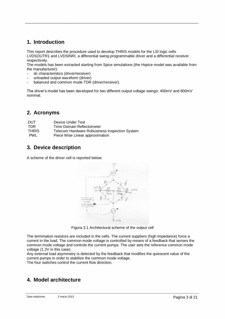
3. Device description A scheme of the driver cell is reported below:
Figura 3.1 Architectural scheme of the output cell
The termination resistors are included in the cells. The current suppliers (high impedance) force a current in the load. The common mode voltage is controlled by means of a feedback that senses the common mode voltage and controls the current pumps. The user sets the reference common mode voltage (1.2V in this case). Any external load asymmetry is detected by the feedback that modifies the quiescent value of the current pumps in order to stabilize the common mode voltage. The four switches control the current flow direction.
4. Model architecture
Data redazione: 2 marzo 2013 Pagina 4 di 21
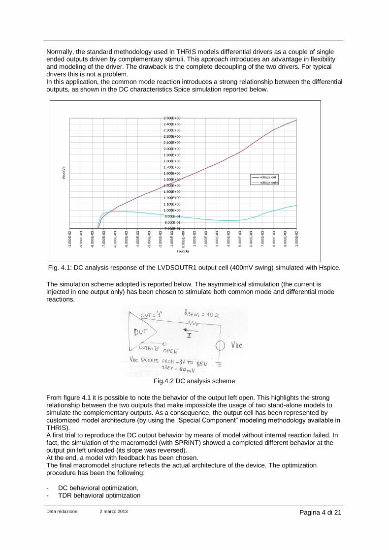
Normally, the standard methodology used in THRIS models differential drivers as a couple of single ended outputs driven by complementary stimuli. This approach introduces an advantage in flexibility and modeling of the driver. The drawback is the complete decoupling of the two drivers. For typical drivers this is not a problem. In this application, the common mode reaction introduces a strong relationship between the differential outputs, as shown in the DC characteristics Spice simulation reported below.
Fig. 4.1: DC analysis response of the LVDSOUTR1 output cell (400mV swing) simulated with Hspice.
The simulation scheme adopted is reported below. The asymmetrical stimulation (the current is injected in one output only) has been chosen to stimulate both common mode and differential mode reactions.
Fig.4.2 DC analysis scheme
From figure 4.1 it is possible to note the behavior of the output left open. This highlights the strong relationship between the two outputs that make impossible the usage of two stand-alone models to simulate the complementary outputs. As a consequence, the output cell has been represented by customized model architecture (by using the “Special Component” modeling methodology available in THRIS). A first trial to reproduce the DC output behavior by means of model without internal reaction failed. In fact, the simulation of the macromodel (with SPRINT) showed a completed different behavior at the output pin left unloaded (its slope was reversed). At the end, a model with feedback has been chosen. The final macromodel structure reflects the actual architecture of the device. The optimization procedure has been the following: - DC behavioral optimization, - TDR behavioral optimization
7.000E-01
8.000E-01
9.000E-01
1.000E+00
1.100E+00
1.200E+00
1.300E+00
1.400E+00
1.500E+00
1.600E+00
1.700E+00
1.800E+00
1.900E+00
2.000E+00
2.100E+00
2.200E+00
2.300E+00
2.400E+00
2.500E+00
-1.0
00E
-02
-9.0
00E
-03
-8.0
00E
-03
-7.0
00E
-03
-6.0
00E
-03
-5.0
00E
-03
-4.0
00E
-03
-3.0
00E
-03
-2.0
00E
-03
-1.0
00E
-03
0.0
00E
+00
1.0
00E
-03
2.0
00E
-03
3.0
00E
-03
4.0
00E
-03
5.0
00E
-03
6.0
00E
-03
7.0
00E
-03
8.0
00E
-03
9.0
00E
-03
1.0
00E
-02
I out (A)
Vo
ut
(V)
voltage out
voltage outn
Data redazione: 2 marzo 2013 Pagina 5 di 21
- Output waveform optimization
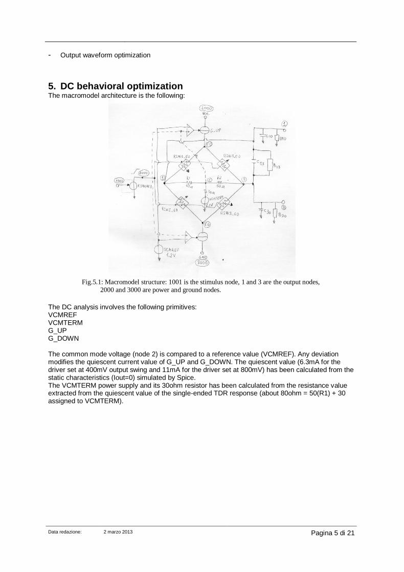
5. DC behavioral optimization The macromodel architecture is the following:
Fig.5.1: Macromodel structure: 1001 is the stimulus node, 1 and 3 are the output nodes,
2000 and 3000 are power and ground nodes.
The DC analysis involves the following primitives: VCMREF VCMTERM G_UP G_DOWN The common mode voltage (node 2) is compared to a reference value (VCMREF). Any deviation modifies the quiescent current value of G_UP and G_DOWN. The quiescent value (6.3mA for the driver set at 400mV output swing and 11mA for the driver set at 800mV) has been calculated from the static characteristics (Iout=0) simulated by Spice. The VCMTERM power supply and its 30ohm resistor has been calculated from the resistance value extracted from the quiescent value of the single-ended TDR response (about 80ohm = 50(R1) + 30 assigned to VCMTERM).
Data redazione: 2 marzo 2013 Pagina 6 di 21
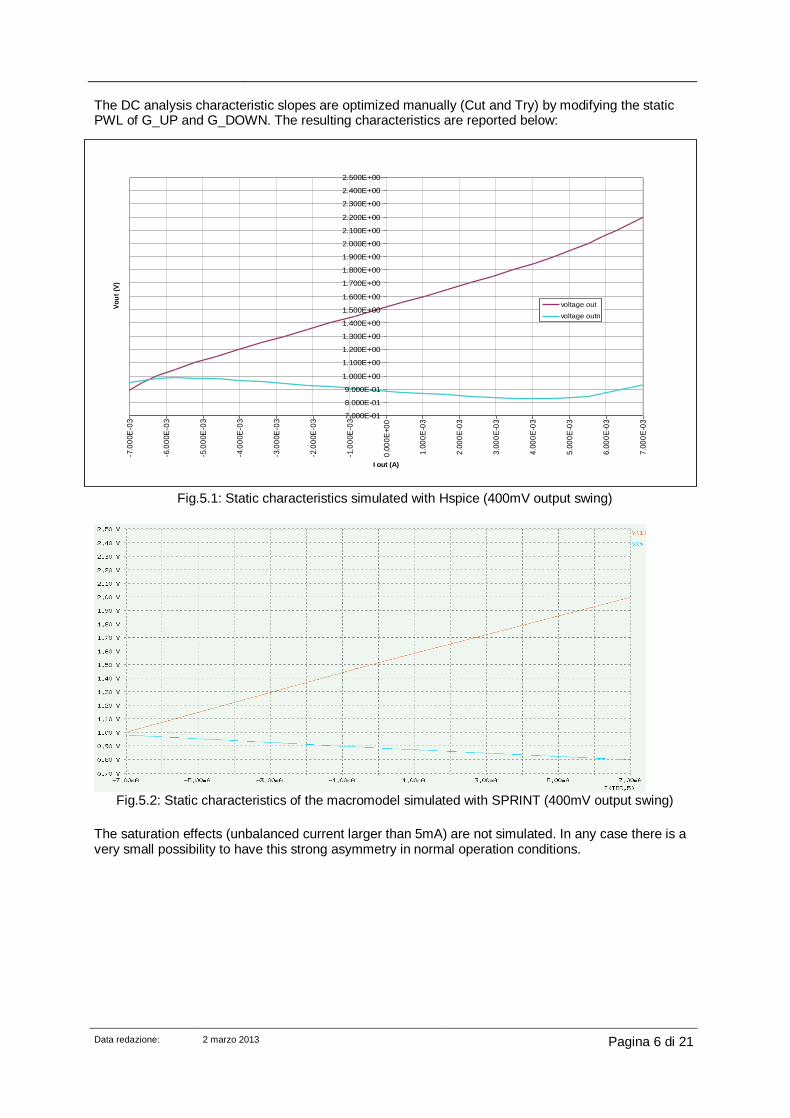
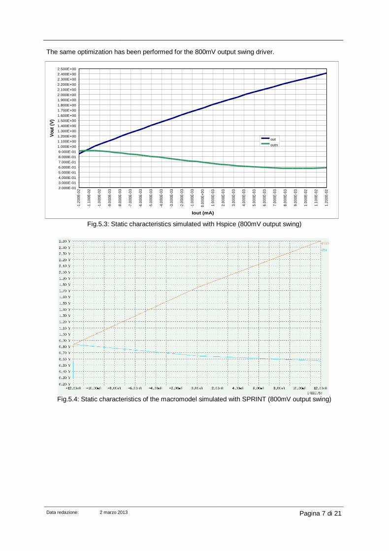
The DC analysis characteristic slopes are optimized manually (Cut and Try) by modifying the static PWL of G_UP and G_DOWN. The resulting characteristics are reported below:
Fig.5.1: Static characteristics simulated with Hspice (400mV output swing)
Fig.5.2: Static characteristics of the macromodel simulated with SPRINT (400mV output swing)
The saturation effects (unbalanced current larger than 5mA) are not simulated. In any case there is a very small possibility to have this strong asymmetry in normal operation conditions.
7.000E-01
8.000E-01
9.000E-01
1.000E+00
1.100E+00
1.200E+00
1.300E+00
1.400E+00
1.500E+00
1.600E+00
1.700E+00
1.800E+00
1.900E+00
2.000E+00
2.100E+00
2.200E+00
2.300E+00
2.400E+00
2.500E+00
-7.0
00E
-03
-6.0
00E
-03
-5.0
00E
-03
-4.0
00E
-03
-3.0
00E
-03
-2.0
00E
-03
-1.0
00E
-03
0.0
00
E+0
0
1.0
00
E-0
3
2.0
00
E-0
3
3.0
00
E-0
3
4.0
00
E-0
3
5.0
00
E-0
3
6.0
00
E-0
3
7.0
00
E-0
3
I out (A)
Vo
ut
(V)
voltage out
voltage outn
Data redazione: 2 marzo 2013 Pagina 7 di 21
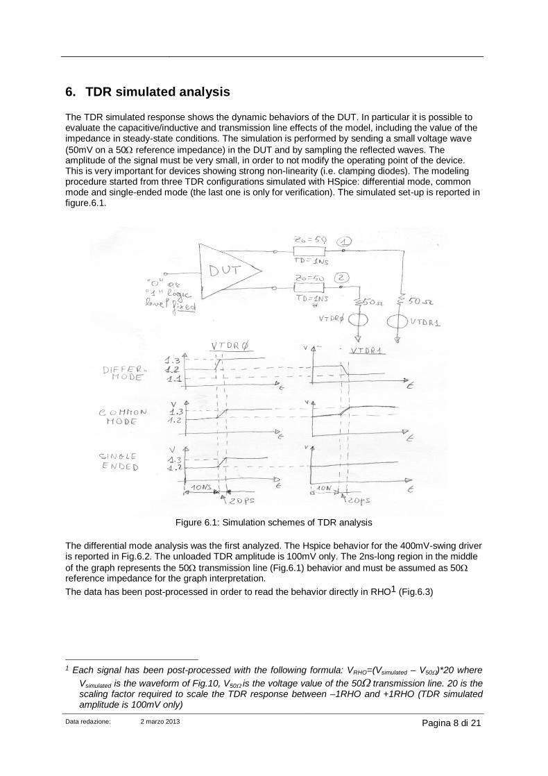
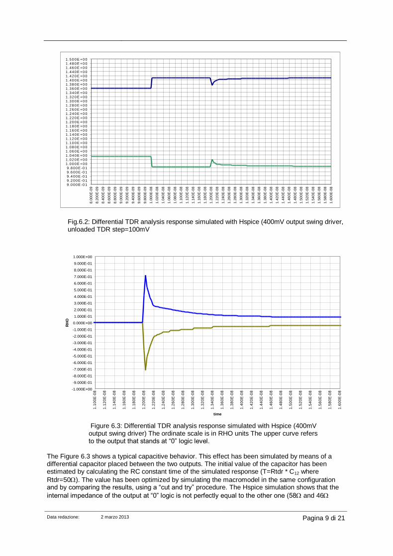
The same optimization has been performed for the 800mV output swing driver.
Fig.5.3: Static characteristics simulated with Hspice (800mV output swing)
Fig.5.4: Static characteristics of the macromodel simulated with SPRINT (800mV output swing)
2.000E-01
3.000E-01
4.000E-01
5.000E-01
6.000E-01
7.000E-01
8.000E-01
9.000E-01
1.000E+00
1.100E+00
1.200E+00
1.300E+00
1.400E+00
1.500E+00
1.600E+00
1.700E+00
1.800E+00
1.900E+00
2.000E+00
2.100E+00
2.200E+00
2.300E+00
2.400E+00
2.500E+00
-1.2
00
E-0
2
-1.1
00
E-0
2
-1.0
00
E-0
2
-9.0
00
E-0
3
-8.0
00
E-0
3
-7.0
00
E-0
3
-6.0
00
E-0
3
-5.0
00
E-0
3
-4.0
00
E-0
3
-3.0
00
E-0
3
-2.0
00
E-0
3
-1.0
00
E-0
3
0.0
00
E+
00
1.0
00
E-0
3
2.0
00
E-0
3
3.0
00
E-0
3
4.0
00
E-0
3
5.0
00
E-0
3
6.0
00
E-0
3
7.0
00
E-0
3
8.0
00
E-0
3
9.0
00
E-0
3
1.0
00
E-0
2
1.1
00
E-0
2
1.2
00
E-0
2
Iout (mA)
Vo
ut
(V)
out
outn
Data redazione: 2 marzo 2013 Pagina 8 di 21
6. TDR simulated analysis The TDR simulated response shows the dynamic behaviors of the DUT. In particular it is possible to evaluate the capacitive/inductive and transmission line effects of the model, including the value of the impedance in steady-state conditions. The simulation is performed by sending a small voltage wave
(50mV on a 50 reference impedance) in the DUT and by sampling the reflected waves. The amplitude of the signal must be very small, in order to not modify the operating point of the device. This is very important for devices showing strong non-linearity (i.e. clamping diodes). The modeling procedure started from three TDR configurations simulated with HSpice: differential mode, common mode and single-ended mode (the last one is only for verification). The simulated set-up is reported in figure.6.1.
Figure 6.1: Simulation schemes of TDR analysis
The differential mode analysis was the first analyzed. The Hspice behavior for the 400mV-swing driver is reported in Fig.6.2. The unloaded TDR amplitude is 100mV only. The 2ns-long region in the middle
of the graph represents the 50 transmission line (Fig.6.1) behavior and must be assumed as 50 reference impedance for the graph interpretation.
The data has been post-processed in order to read the behavior directly in RHO1 (Fig.6.3)
1 Each signal has been post-processed with the following formula: VRHO=(Vsimulated – V50)*20 where
Vsimulated is the waveform of Fig.10, V50 is the voltage value of the 50 transmission line. 20 is the scaling factor required to scale the TDR response between –1RHO and +1RHO (TDR simulated amplitude is 100mV only)
Data redazione: 2 marzo 2013 Pagina 9 di 21
Fig.6.2: Differential TDR analysis response simulated with Hspice (400mV output swing driver, unloaded TDR step=100mV
-1.000E+00
-9.000E-01
-8.000E-01
-7.000E-01
-6.000E-01
-5.000E-01
-4.000E-01
-3.000E-01
-2.000E-01
-1.000E-01
0.000E+00
1.000E-01
2.000E-01
3.000E-01
4.000E-01
5.000E-01
6.000E-01
7.000E-01
8.000E-01
9.000E-01
1.000E+00
1.1
00
E-0
8
1.1
20
E-0
8
1.1
40
E-0
8
1.1
60
E-0
8
1.1
80
E-0
8
1.2
00
E-0
8
1.2
20
E-0
8
1.2
40
E-0
8
1.2
60
E-0
8
1.2
80
E-0
8
1.3
00
E-0
8
1.3
20
E-0
8
1.3
40
E-0
8
1.3
60
E-0
8
1.3
80
E-0
8
1.4
00
E-0
8
1.4
20
E-0
8
1.4
40
E-0
8
1.4
60
E-0
8
1.4
80
E-0
8
1.5
00
E-0
8
1.5
20
E-0
8
1.5
40
E-0
8
1.5
60
E-0
8
1.5
80
E-0
8
1.6
00
E-0
8
time
RH
O
Figure 6.3: Differential TDR analysis response simulated with Hspice (400mV output swing driver) The ordinate scale is in RHO units The upper curve refers to the output that stands at “0” logic level.
The Figure 6.3 shows a typical capacitive behavior. This effect has been simulated by means of a differential capacitor placed between the two outputs. The initial value of the capacitor has been estimated by calculating the RC constant time of the simulated response (T=Rtdr * C12 where
Rtdr=50). The value has been optimized by simulating the macromodel in the same configuration and by comparing the results, using a “cut and try” procedure. The Hspice simulation shows that the
internal impedance of the output at “0” logic is not perfectly equal to the other one (58 and 46
9 .0 0 0 E -0 19 .2 0 0 E -0 19 .4 0 0 E -0 19 .6 0 0 E -0 19 .8 0 0 E -0 1
1 .00 0 E +0 01 .02 0 E +0 01 .04 0 E +0 0
1 .06 0 E +0 01 .08 0 E +0 01 .10 0 E +0 01 .12 0 E +0 01 .14 0 E +0 01 .16 0 E +0 01 .18 0 E +0 01 .20 0 E +0 01 .22 0 E +0 01 .24 0 E +0 01 .26 0 E +0 01 .28 0 E +0 01 .30 0 E +0 01 .32 0 E +0 01 .34 0 E +0 0
1 .36 0 E +0 01 .38 0 E +0 01 .40 0 E +0 01 .42 0 E +0 01 .44 0 E +0 01 .46 0 E +0 01 .48 0 E +0 01 .50 0 E +0 0
8.0
00
E-0
9
8.2
00
E-0
9
8.4
00
E-0
9
8.6
00
E-0
9
8.8
00
E-0
9
9.0
00
E-0
9
9.2
00
E-0
9
9.4
00
E-0
9
9.6
00
E-0
9
9.8
00
E-0
9
1.0
00
E-0
8
1.0
20
E-0
8
1.0
40
E-0
8
1.0
60
E-0
8
1.0
80
E-0
8
1.1
00
E-0
8
1.1
20
E-0
8
1.1
40
E-0
8
1.1
60
E-0
8
1.1
80
E-0
8
1.2
00
E-0
8
1.2
20
E-0
8
1.2
40
E-0
8
1.2
60
E-0
8
1.2
80
E-0
8
1.3
00
E-0
8
1.3
20
E-0
8
1.3
40
E-0
8
1.3
60
E-0
8
1.3
80
E-0
8
1.4
00
E-0
8
1.4
20
E-0
8
1.4
40
E-0
8
1.4
60
E-0
8
1.4
80
E-0
8
1.5
00
E-0
8
1.5
20
E-0
8
1.5
40
E-0
8
1.5
60
E-0
8
1.5
80
E-0
8
1.6
00
E-0
8
Data redazione: 2 marzo 2013 Pagina 10 di 21
respectively). However, the two resistances have been assumed both equal to 50 in the THRIS
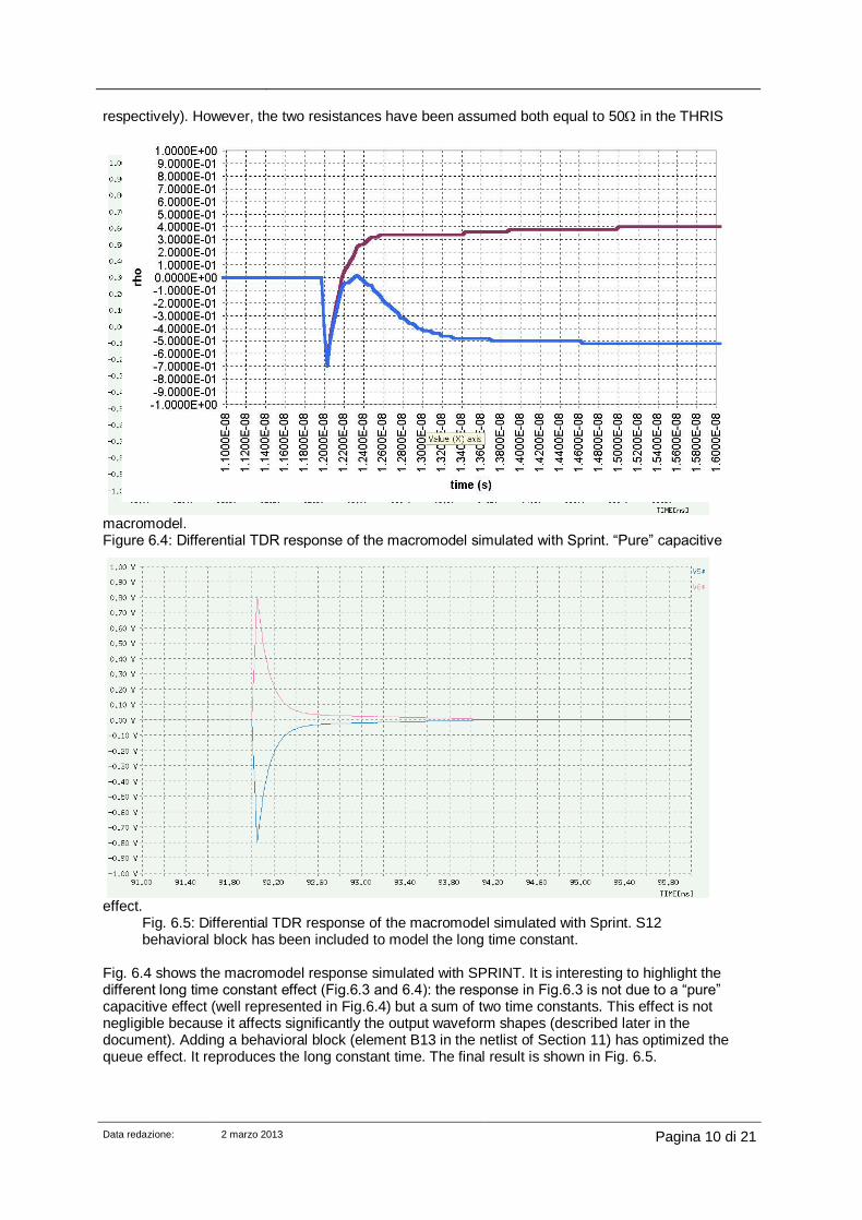
macromodel. Figure 6.4: Differential TDR response of the macromodel simulated with Sprint. “Pure” capacitive
effect. Fig. 6.5: Differential TDR response of the macromodel simulated with Sprint. S12 behavioral block has been included to model the long time constant.
Fig. 6.4 shows the macromodel response simulated with SPRINT. It is interesting to highlight the different long time constant effect (Fig.6.3 and 6.4): the response in Fig.6.3 is not due to a “pure” capacitive effect (well represented in Fig.6.4) but a sum of two time constants. This effect is not negligible because it affects significantly the output waveform shapes (described later in the document). Adding a behavioral block (element B13 in the netlist of Section 11) has optimized the queue effect. It reproduces the long constant time. The final result is shown in Fig. 6.5.
Data redazione: 2 marzo 2013 Pagina 11 di 21
Figure.6.6: Common mode TDR analysis response simulated with Hspice (400mV output swing driver). Ordinate scale is in RHO units. The upper curve refers to the output that stands at “1” logic level.
The common mode TDR response (as resulting from the post-processing procedure already described for the differential TDR) simulated with Hspice is reported in Fig.6.6.
It is interesting to note that the behavior of the two outputs is quite different. This is due to the common mode feedback. While the “1” logic level behavior is quite similar to a capacitive effect, the “0” logic level tries, at the beginning” to follow” an identical behavior, but after 200-400ps the common mode reaction forces the output voltage to decrease. The macromodel behavior simulated with Sprint is reported in Fig.6.7, where a unbalanced capacitor has been added to each output of the device under test (2pf each), as well as a behavioral elements (B10 and B30) to reproduce the long time constant effect. It is interesting to note that the bounce on the output at “0” logic level is smoothed. In fact, in the macromodel the common mode feedback loop has no artificial delay and it results too fast. Two behavioral, smoothing-effect, elements introduced in the G_UP and G_DOWN current generators (by means of a s(t)=… dynamic statement) increase the model accuracy. The final response of the macromodel is reported in Fig.6.8.
Data redazione: 2 marzo 2013 Pagina 12 di 21
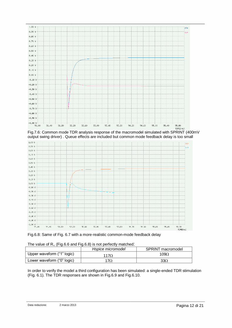
Fig.7.6: Common mode TDR analysis response of the macromodel simulated with SPRINT (400mV output swing driver) . Queue effects are included but common mode feedback delay is too small
Fig.6.8: Same of Fig. 6.7 with a more-realistic common-mode feedback delay
The value of R (Fig.6.6 and Fig.6.8) is not perfectly matched: Hspice micromodel SPRINT macromodel
Upper waveform (“1” logic) 117 109
Lower waveform (“0” logic) 17 33
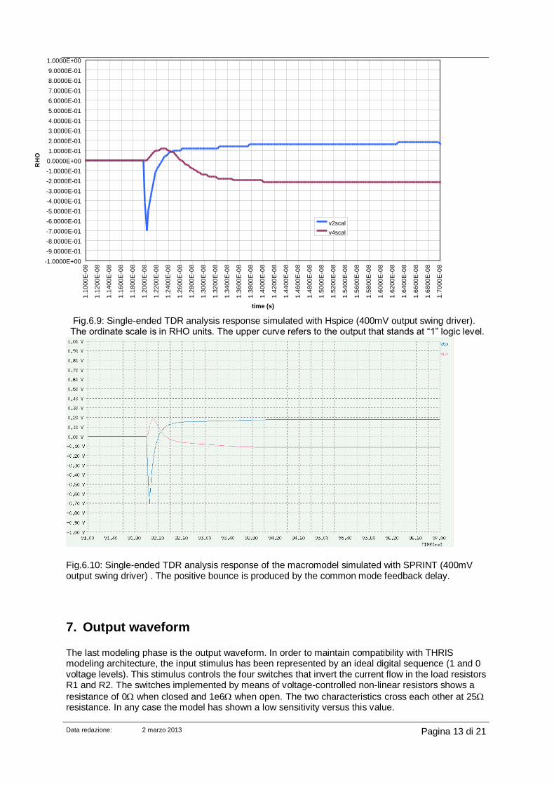
In order to verify the model a third configuration has been simulated: a single-ended TDR stimulation (Fig. 6.1). The TDR responses are shown in Fig.6.9 and Fig.6.10.
Data redazione: 2 marzo 2013 Pagina 13 di 21
Fig.6.9: Single-ended TDR analysis response simulated with Hspice (400mV output swing driver). The ordinate scale is in RHO units. The upper curve refers to the output that stands at “1” logic level.
Fig.6.10: Single-ended TDR analysis response of the macromodel simulated with SPRINT (400mV output swing driver) . The positive bounce is produced by the common mode feedback delay.
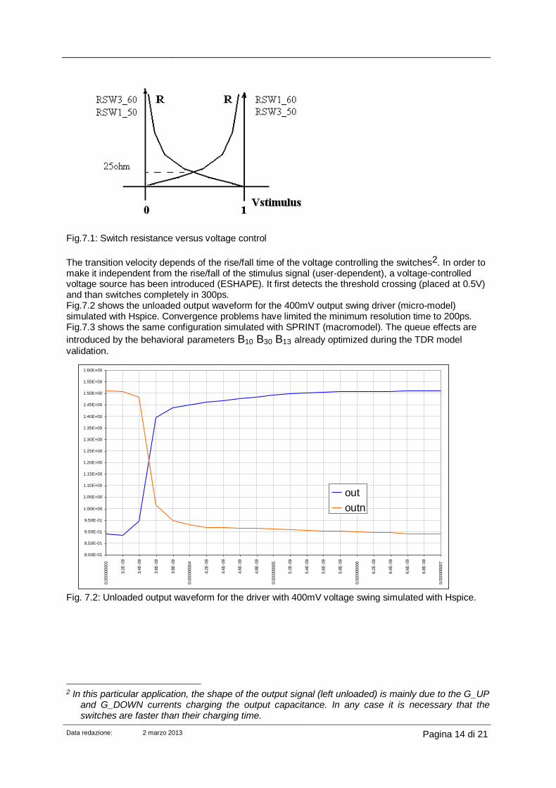
7. Output waveform The last modeling phase is the output waveform. In order to maintain compatibility with THRIS modeling architecture, the input stimulus has been represented by an ideal digital sequence (1 and 0 voltage levels). This stimulus controls the four switches that invert the current flow in the load resistors R1 and R2. The switches implemented by means of voltage-controlled non-linear resistors shows a
resistance of 0 when closed and 1e6 when open. The two characteristics cross each other at 25 resistance. In any case the model has shown a low sensitivity versus this value.
-1.0000E+00
-9.0000E-01
-8.0000E-01
-7.0000E-01
-6.0000E-01
-5.0000E-01
-4.0000E-01
-3.0000E-01
-2.0000E-01
-1.0000E-01
0.0000E+00
1.0000E-01
2.0000E-01
3.0000E-01
4.0000E-01
5.0000E-01
6.0000E-01
7.0000E-01
8.0000E-01
9.0000E-01
1.0000E+00
1.1
00
0E
-08
1.1
20
0E
-08
1.1
40
0E
-08
1.1
60
0E
-08
1.1
80
0E
-08
1.2
00
0E
-08
1.2
20
0E
-08
1.2
40
0E
-08
1.2
60
0E
-08
1.2
80
0E
-08
1.3
00
0E
-08
1.3
20
0E
-08
1.3
40
0E
-08
1.3
60
0E
-08
1.3
80
0E
-08
1.4
00
0E
-08
1.4
20
0E
-08
1.4
40
0E
-08
1.4
60
0E
-08
1.4
80
0E
-08
1.5
00
0E
-08
1.5
20
0E
-08
1.5
40
0E
-08
1.5
60
0E
-08
1.5
80
0E
-08
1.6
00
0E
-08
1.6
20
0E
-08
1.6
40
0E
-08
1.6
60
0E
-08
1.6
80
0E
-08
1.7
00
0E
-08
time (s)
RH
O
v2scal
v4scal
Data redazione: 2 marzo 2013 Pagina 14 di 21
Fig.7.1: Switch resistance versus voltage control
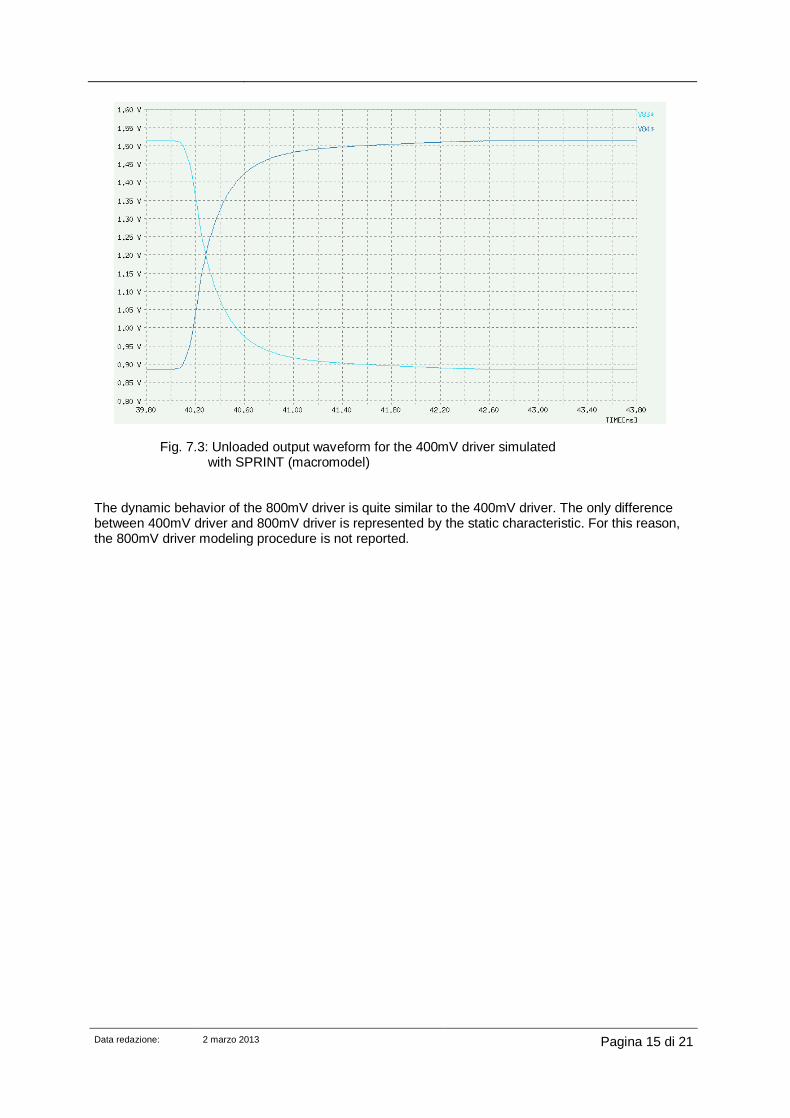
The transition velocity depends of the rise/fall time of the voltage controlling the switches2. In order to make it independent from the rise/fall of the stimulus signal (user-dependent), a voltage-controlled voltage source has been introduced (ESHAPE). It first detects the threshold crossing (placed at 0.5V) and than switches completely in 300ps. Fig.7.2 shows the unloaded output waveform for the 400mV output swing driver (micro-model) simulated with Hspice. Convergence problems have limited the minimum resolution time to 200ps. Fig.7.3 shows the same configuration simulated with SPRINT (macromodel). The queue effects are
introduced by the behavioral parameters B10 B30 B13 already optimized during the TDR model
validation.
Fig. 7.2: Unloaded output waveform for the driver with 400mV voltage swing simulated with Hspice.
2 In this particular application, the shape of the output signal (left unloaded) is mainly due to the G_UP
and G_DOWN currents charging the output capacitance. In any case it is necessary that the switches are faster than their charging time.
8.00E-01
8.50E-01
9.00E-01
9.50E-01
1.00E+00
1.05E+00
1.10E+00
1.15E+00
1.20E+00
1.25E+00
1.30E+00
1.35E+00
1.40E+00
1.45E+00
1.50E+00
1.55E+00
1.60E+00
0.0
00
000003
3.2
E-0
9
3.4
E-0
9
3.6
E-0
9
3.8
E-0
9
0.0
00
000004
4.2
E-0
9
4.4
E-0
9
4.6
E-0
9
4.8
E-0
9
0.0
00
000005
5.2
E-0
9
5.4
E-0
9
5.6
E-0
9
5.8
E-0
9
0.0
00
000006
6.2
E-0
9
6.4
E-0
9
6.6
E-0
9
6.8
E-0
9
0.0
00
000007
out
outn
Data redazione: 2 marzo 2013 Pagina 15 di 21
Fig. 7.3: Unloaded output waveform for the 400mV driver simulated with SPRINT (macromodel)
The dynamic behavior of the 800mV driver is quite similar to the 400mV driver. The only difference between 400mV driver and 800mV driver is represented by the static characteristic. For this reason, the 800mV driver modeling procedure is not reported.
Data redazione: 2 marzo 2013 Pagina 16 di 21
8. Differential receiver VI characteristic The receiver has a very simple topology, as described below:
Fig.8.1: Differential input architecture.
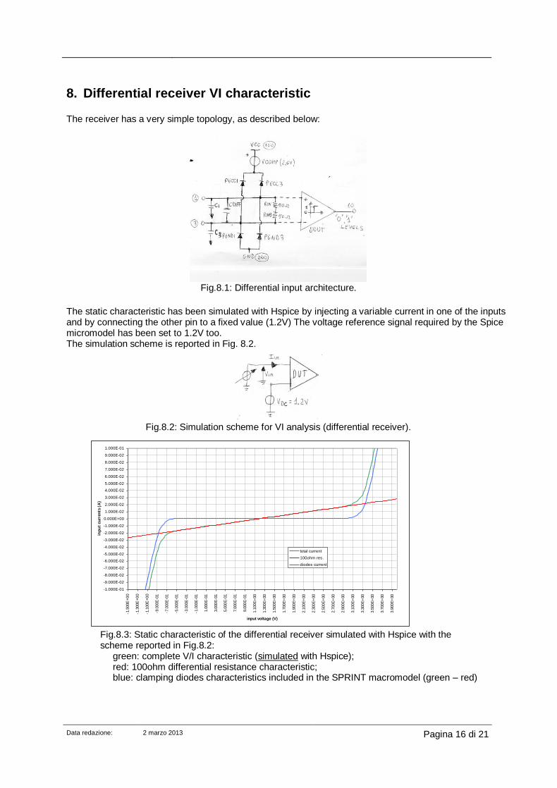
The static characteristic has been simulated with Hspice by injecting a variable current in one of the inputs and by connecting the other pin to a fixed value (1.2V) The voltage reference signal required by the Spice micromodel has been set to 1.2V too. The simulation scheme is reported in Fig. 8.2.
Fig.8.2: Simulation scheme for VI analysis (differential receiver).
Fig.8.3: Static characteristic of the differential receiver simulated with Hspice with the scheme reported in Fig.8.2:
green: complete V/I characteristic (simulated with Hspice); red: 100ohm differential resistance characteristic; blue: clamping diodes characteristics included in the SPRINT macromodel (green – red)
-1.000E-01
-9.000E-02
-8.000E-02
-7.000E-02
-6.000E-02
-5.000E-02
-4.000E-02
-3.000E-02
-2.000E-02
-1.000E-02
0.000E+00
1.000E-02
2.000E-02
3.000E-02
4.000E-02
5.000E-02
6.000E-02
7.000E-02
8.000E-02
9.000E-02
1.000E-01
-1.5
00E
+0
0
-1.3
00E
+0
0
-1.1
00E
+0
0
-9.0
00E
-01
-7.0
00E
-01
-5.0
00E
-01
-3.0
00E
-01
-1.0
00E
-01
1.0
00
E-0
1
3.0
00
E-0
1
5.0
00
E-0
1
7.0
00
E-0
1
9.0
00
E-0
1
1.1
00
E+
00
1.3
00
E+
00
1.5
00
E+
00
1.7
00
E+
00
1.9
00
E+
00
2.1
00
E+
00
2.3
00
E+
00
2.5
00
E+
00
2.7
00
E+
00
2.9
00
E+
00
3.1
00
E+
00
3.3
00
E+
00
3.5
00
E+
00
3.7
00
E+
00
3.9
00
E+
00
input voltage (V)
inp
ut
cu
rren
ts (
A)
total current
100ohm res.
diodes current
Data redazione: 2 marzo 2013 Pagina 17 di 21
In the SPRINT macromodel the measured waveform (Fig.8.3 – green curve) has been represented by a sum of two characteristics, one due the termination resistor of 100 (red) and one due the “pure” clamping diode effect (blue).
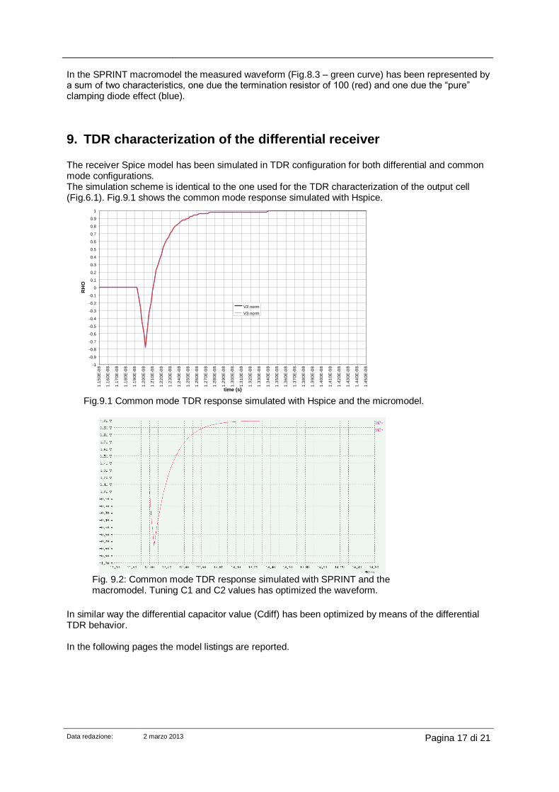
9. TDR characterization of the differential receiver The receiver Spice model has been simulated in TDR configuration for both differential and common mode configurations. The simulation scheme is identical to the one used for the TDR characterization of the output cell (Fig.6.1). Fig.9.1 shows the common mode response simulated with Hspice.
Fig.9.1 Common mode TDR response simulated with Hspice and the micromodel.
Fig. 9.2: Common mode TDR response simulated with SPRINT and the macromodel. Tuning C1 and C2 values has optimized the waveform.
In similar way the differential capacitor value (Cdiff) has been optimized by means of the differential TDR behavior. In the following pages the model listings are reported.
-1
-0.9
-0.8
-0.7
-0.6
-0.5
-0.4
-0.3
-0.2
-0.1
0
0.1
0.2
0.3
0.4
0.5
0.6
0.7
0.8
0.9
1
1.1
50
E-0
8
1.1
60
E-0
8
1.1
70
E-0
8
1.1
80
E-0
8
1.1
90
E-0
8
1.2
00
E-0
8
1.2
10
E-0
8
1.2
20
E-0
8
1.2
30
E-0
8
1.2
40
E-0
8
1.2
50
E-0
8
1.2
60
E-0
8
1.2
70
E-0
8
1.2
80
E-0
8
1.2
90
E-0
8
1.3
00
E-0
8
1.3
10
E-0
8
1.3
20
E-0
8
1.3
30
E-0
8
1.3
40
E-0
8
1.3
50
E-0
8
1.3
60
E-0
8
1.3
70
E-0
8
1.3
80
E-0
8
1.3
90
E-0
8
1.4
00
E-0
8
1.4
10
E-0
8
1.4
20
E-0
8
1.4
30
E-0
8
1.4
40
E-0
8
1.4
50
E-0
8
time (s)
RH
O
V2 norm
V3 norm
Data redazione: 2 marzo 2013 Pagina 18 di 21
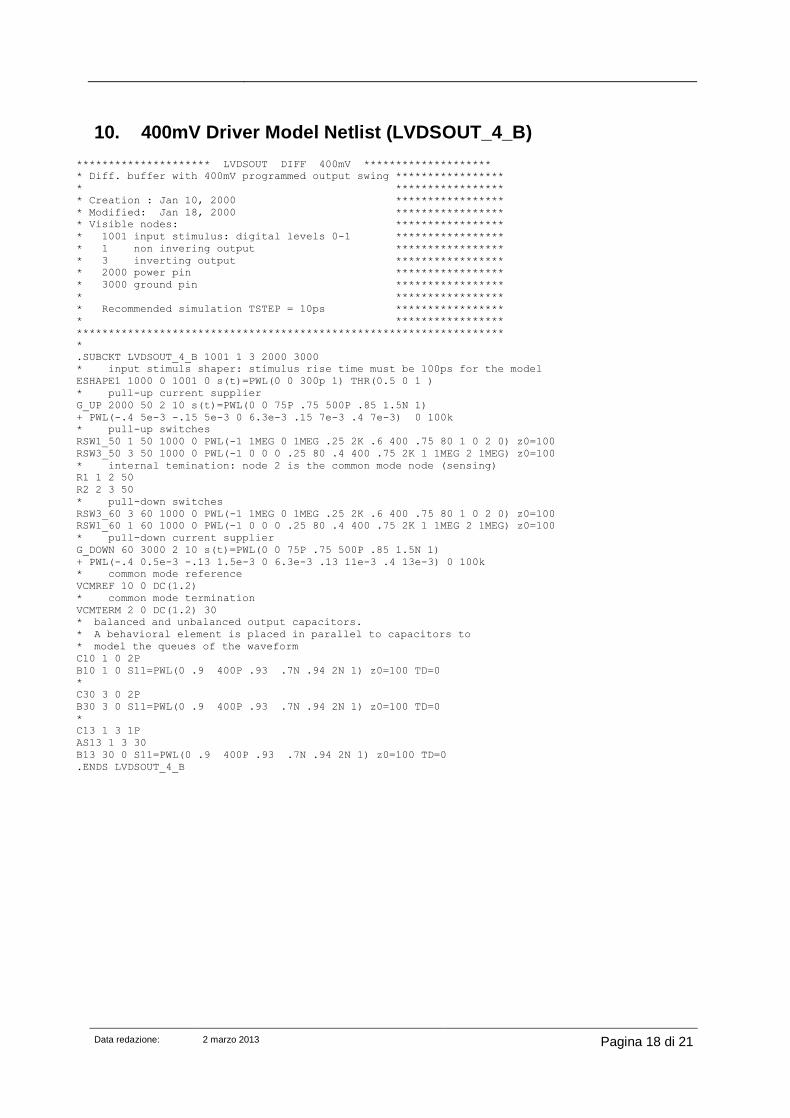
10. 400mV Driver Model Netlist (LVDSOUT_4_B)
********************* LVDSOUT DIFF 400mV ********************
* Diff. buffer with 400mV programmed output swing *****************
* *****************
* Creation : Jan 10, 2000 *****************
* Modified: Jan 18, 2000 *****************
* Visible nodes: *****************
* 1001 input stimulus: digital levels 0-1 *****************
* 1 non invering output *****************
* 3 inverting output *****************
* 2000 power pin *****************
* 3000 ground pin *****************
* *****************
* Recommended simulation TSTEP = 10ps *****************
* *****************
*******************************************************************
*
.SUBCKT LVDSOUT_4_B 1001 1 3 2000 3000
* input stimuls shaper: stimulus rise time must be 100ps for the model
ESHAPE1 1000 0 1001 0 s(t)=PWL(0 0 300p 1) THR(0.5 0 1 )
* pull-up current supplier
G_UP 2000 50 2 10 s(t)=PWL(0 0 75P .75 500P .85 1.5N 1)
+ PWL(-.4 5e-3 -.15 5e-3 0 6.3e-3 .15 7e-3 .4 7e-3) 0 100k
* pull-up switches
RSW1_50 1 50 1000 0 PWL(-1 1MEG 0 1MEG .25 2K .6 400 .75 80 1 0 2 0) z0=100
RSW3_50 3 50 1000 0 PWL(-1 0 0 0 .25 80 .4 400 .75 2K 1 1MEG 2 1MEG) z0=100
* internal temination: node 2 is the common mode node (sensing)
R1 1 2 50
R2 2 3 50
* pull-down switches
RSW3_60 3 60 1000 0 PWL(-1 1MEG 0 1MEG .25 2K .6 400 .75 80 1 0 2 0) z0=100
RSW1_60 1 60 1000 0 PWL(-1 0 0 0 .25 80 .4 400 .75 2K 1 1MEG 2 1MEG) z0=100
* pull-down current supplier
G_DOWN 60 3000 2 10 s(t)=PWL(0 0 75P .75 500P .85 1.5N 1)
+ PWL(-.4 0.5e-3 -.13 1.5e-3 0 6.3e-3 .13 11e-3 .4 13e-3) 0 100k
* common mode reference
VCMREF 10 0 DC(1.2)
* common mode termination
VCMTERM 2 0 DC(1.2) 30
* balanced and unbalanced output capacitors.
* A behavioral element is placed in parallel to capacitors to
* model the queues of the waveform
C10 1 0 2P
B10 1 0 S11=PWL(0 .9 400P .93 .7N .94 2N 1) z0=100 TD=0
*
C30 3 0 2P
B30 3 0 S11=PWL(0 .9 400P .93 .7N .94 2N 1) z0=100 TD=0
*
C13 1 3 1P
AS13 1 3 30
B13 30 0 S11=PWL(0 .9 400P .93 .7N .94 2N 1) z0=100 TD=0
.ENDS LVDSOUT_4_B
Data redazione: 2 marzo 2013 Pagina 19 di 21
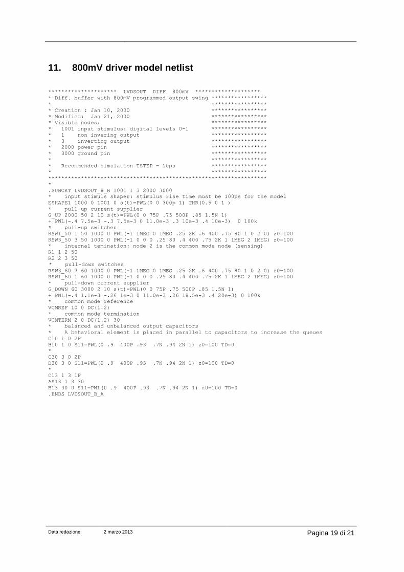
11. 800mV driver model netlist ********************* LVDSOUT DIFF 800mV ********************
* Diff. buffer with 800mV programmed output swing *****************
* *****************
* Creation : Jan 10, 2000 *****************
* Modified: Jan 21, 2000 *****************
* Visible nodes: *****************
* 1001 input stimulus: digital levels 0-1 *****************
* 1 non invering output *****************
* 3 inverting output *****************
* 2000 power pin *****************
* 3000 ground pin *****************
* *****************
* Recommended simulation TSTEP = 10ps *****************
* *****************
*******************************************************************
*
.SUBCKT LVDSOUT_8_B 1001 1 3 2000 3000
* input stimuls shaper: stimulus rise time must be 100ps for the model
ESHAPE1 1000 0 1001 0 s(t)=PWL(0 0 300p 1) THR(0.5 0 1 )
* pull-up current supplier
G_UP 2000 50 2 10 s(t)=PWL(0 0 75P .75 500P .85 1.5N 1)
+ PWL(-.4 7.5e-3 -.3 7.5e-3 0 11.0e-3 .3 10e-3 .4 10e-3) 0 100k
* pull-up switches
RSW1_50 1 50 1000 0 PWL(-1 1MEG 0 1MEG .25 2K .6 400 .75 80 1 0 2 0) z0=100
RSW3_50 3 50 1000 0 PWL(-1 0 0 0 .25 80 .4 400 .75 2K 1 1MEG 2 1MEG) z0=100
* internal temination: node 2 is the common mode node (sensing)
R1 1 2 50
R2 2 3 50
* pull-down switches
RSW3_60 3 60 1000 0 PWL(-1 1MEG 0 1MEG .25 2K .6 400 .75 80 1 0 2 0) z0=100
RSW1_60 1 60 1000 0 PWL(-1 0 0 0 .25 80 .4 400 .75 2K 1 1MEG 2 1MEG) z0=100
* pull-down current supplier
G_DOWN 60 3000 2 10 s(t)=PWL(0 0 75P .75 500P .85 1.5N 1)
+ PWL(-.4 1.1e-3 -.26 1e-3 0 11.0e-3 .26 18.5e-3 .4 20e-3) 0 100k
* common mode reference
VCMREF 10 0 DC(1.2)
* common mode termination
VCMTERM 2 0 DC(1.2) 30
* balanced and unbalanced output capacitors
* A behavioral element is placed in parallel to capacitors to increase the queues
C10 1 0 2P
B10 1 0 S11=PWL(0 .9 400P .93 .7N .94 2N 1) z0=100 TD=0
*
C30 3 0 2P
B30 3 0 S11=PWL(0 .9 400P .93 .7N .94 2N 1) z0=100 TD=0
*
C13 1 3 1P
AS13 1 3 30
B13 30 0 S11=PWL(0 .9 400P .93 .7N .94 2N 1) z0=100 TD=0
.ENDS LVDSOUT_B_A
Data redazione: 2 marzo 2013 Pagina 20 di 21
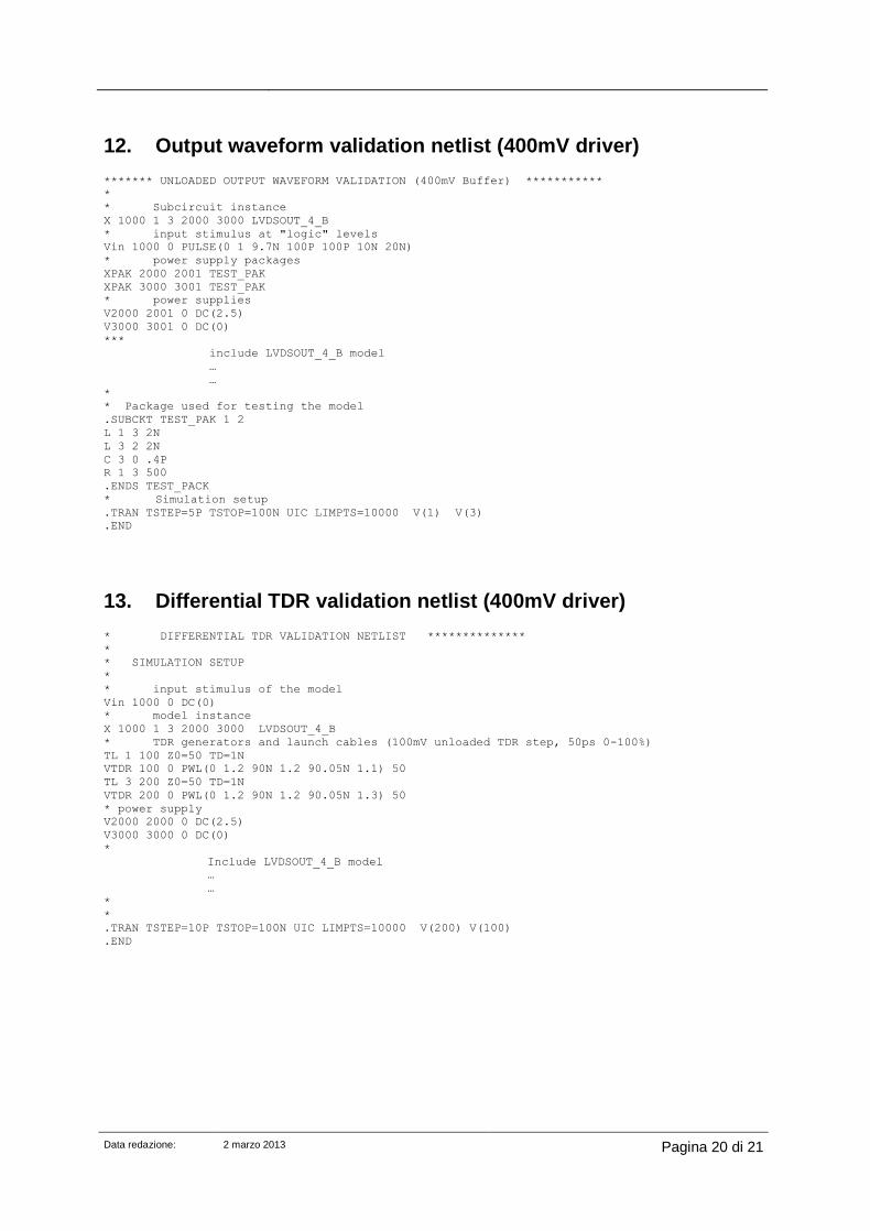
12. Output waveform validation netlist (400mV driver) ******* UNLOADED OUTPUT WAVEFORM VALIDATION (400mV Buffer) ***********
*
* Subcircuit instance
X 1000 1 3 2000 3000 LVDSOUT_4_B
* input stimulus at "logic" levels
Vin 1000 0 PULSE(0 1 9.7N 100P 100P 10N 20N)
* power supply packages
XPAK 2000 2001 TEST_PAK
XPAK 3000 3001 TEST_PAK
* power supplies
V2000 2001 0 DC(2.5)
V3000 3001 0 DC(0)
***
include LVDSOUT_4_B model
…
…
*
* Package used for testing the model
.SUBCKT TEST_PAK 1 2
L 1 3 2N
L 3 2 2N
C 3 0 .4P
R 1 3 500
.ENDS TEST_PACK
* Simulation setup
.TRAN TSTEP=5P TSTOP=100N UIC LIMPTS=10000 V(1) V(3)
.END
13. Differential TDR validation netlist (400mV driver) * DIFFERENTIAL TDR VALIDATION NETLIST **************
*
* SIMULATION SETUP
*
* input stimulus of the model
Vin 1000 0 DC(0)
* model instance
X 1000 1 3 2000 3000 LVDSOUT_4_B
* TDR generators and launch cables (100mV unloaded TDR step, 50ps 0-100%)
TL 1 100 Z0=50 TD=1N
VTDR 100 0 PWL(0 1.2 90N 1.2 90.05N 1.1) 50
TL 3 200 Z0=50 TD=1N
VTDR 200 0 PWL(0 1.2 90N 1.2 90.05N 1.3) 50
* power supply
V2000 2000 0 DC(2.5)
V3000 3000 0 DC(0)
*
Include LVDSOUT_4_B model
…
…
*
*
.TRAN TSTEP=10P TSTOP=100N UIC LIMPTS=10000 V(200) V(100)
.END
Data redazione: 2 marzo 2013 Pagina 21 di 21
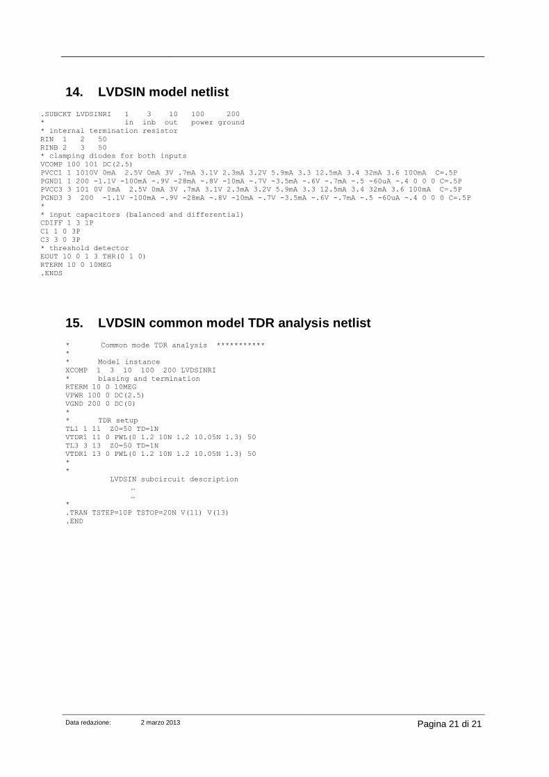
14. LVDSIN model netlist
.SUBCKT LVDSINRI 1 3 10 100 200
* in inb out power ground
* internal termination resistor
RIN 1 2 50
RINB 2 3 50
* clamping diodes for both inputs
VCOMP 100 101 DC(2.5)
PVCC1 1 1010V 0mA 2.5V 0mA 3V .7mA 3.1V 2.3mA 3.2V 5.9mA 3.3 12.5mA 3.4 32mA 3.6 100mA C=.5P
PGND1 1 200 -1.1V -100mA -.9V -28mA -.8V -10mA -.7V -3.5mA -.6V -.7mA -.5 -60uA -.4 0 0 0 C=.5P
PVCC3 3 101 0V 0mA 2.5V 0mA 3V .7mA 3.1V 2.3mA 3.2V 5.9mA 3.3 12.5mA 3.4 32mA 3.6 100mA C=.5P
PGND3 3 200 -1.1V -100mA -.9V -28mA -.8V -10mA -.7V -3.5mA -.6V -.7mA -.5 -60uA -.4 0 0 0 C=.5P
*
* input capacitors (balanced and differential)
CDIFF 1 3 1P
C1 1 0 3P
C3 3 0 3P
* threshold detector
EOUT 10 0 1 3 THR(0 1 0)
RTERM 10 0 10MEG
.ENDS
15. LVDSIN common model TDR analysis netlist * Common mode TDR analysis ***********
*
* Model instance
XCOMP 1 3 10 100 200 LVDSINRI
* biasing and termination
RTERM 10 0 10MEG
VPWR 100 0 DC(2.5)
VGND 200 0 DC(0)
*
* TDR setup
TL1 1 11 Z0=50 TD=1N
VTDR1 11 0 PWL(0 1.2 10N 1.2 10.05N 1.3) 50
TL3 3 13 Z0=50 TD=1N
VTDR1 13 0 PWL(0 1.2 10N 1.2 10.05N 1.3) 50
*
*
LVDSIN subcircuit description
…
…
*
.TRAN TSTEP=10P TSTOP=20N V(11) V(13)
.END