sn65lvds10x 4-port lvds and 4-port ttl-to-lvds repeaters
TRANSCRIPT
4Z
4Y
3Z
3Y
2Z
2Y
1Z
1Y
EN1
EN2
A
EN4
EN3
4Z
4Y
3Z
3Y
2Z
2Y
1Z
1Y
EN1
EN2
A
EN4
EN3
B
Product
Folder
Sample &Buy
Technical
Documents
Tools &
Software
Support &Community
SN65LVDS104, SN65LVDS105SLLS396G –SEPTEMBER 1999–REVISED DECEMBER 2015
SN65LVDS10x 4-Port LVDS and 4-Port TTL-to-LVDS Repeaters1 Features 3 Description
The SN65LVDS10x are a differential line receiver and1• Receiver and Drivers Meet or Exceed the
a LVTTL input (respectively) connected to fourRequirements of ANSI EIA/TIA-644 Standarddifferential line drivers that implement the electrical
– SN65LVDS105 Receives Low-Voltage TTL characteristics of low-voltage differential signaling(LVTTL) Levels (LVDS). LVDS, as specified in EIA/TIA-644 is a data
signaling technique that offers low-power, low-noise– SN65LVDS104 Receives Differential Inputcoupling, and switching speeds to transmit data atLevels, ±100 mVrelatively long distances. (Note: The ultimate rate and• Typical Data Signaling Rates to 400 Mbps or distance of data transfer is dependent upon theClock Frequencies to 400 MHz attenuation characteristics of the media, the noise
• Operates From a Single 3.3-V Supply coupling to the environment, and other systemcharacteristics.)• Low-Voltage Differential Signaling With Typical
Output Voltage of 350 mV and a 100-Ω Load The intended application of this device and signaling• Propagation Delay Time technique is for point-to-point baseband data
transmission over controlled impedance media of– SN65LVDS105 – 2.2 ns (Typ)approximately 100 Ω. The transmission media may– SN65LVDS104 – 3.1 ns (Typ) be printed-circuit board traces, backplanes, or cables.
• LVTTL Levels Are 5-V Tolerant Having the drivers integrated into the same substrate,along with the low pulse skew of balanced signaling,• Electrically Compatible With LVDS, PECL,allows extremely precise timing alignment of theLVPECL, LVTTL, LVCMOS, GTL, BTL, CTT,signals repeated from the input. This is particularlySSTL, or HSTL Outputs With External Networksadvantageous in distribution or expansion of signals
• Driver Outputs Are High-Impedance When such as clock or serial data stream.Disabled or With VCC <1.5 V
The SN65LVDS10x are characterized for operation• Bus-Pin ESD Protection Exceeds 16 kV from –40°C to 85°C.• SOIC and TSSOP Packaging
The SN65LVDS10x are members of a family of LVDSrepeaters. A brief overview of the family is provided in2 Applications the Selection Guide to LVDS Repeaters section.
• Clock DistributionDevice Information(1)• Wireless Base Stations
PART NUMBER PACKAGE BODY SIZE (NOM)• Network RoutersSOIC (16) 9.90 mm × 3.91 mmSN65LVDS104,
SN65LVDS105 TSSOP (16) 5.00 mm × 4.40 mm
(1) For all available packages, see the orderable addendum atthe end of the data sheet.
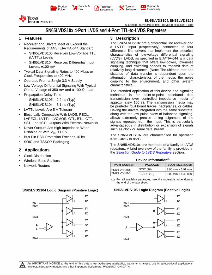
SN65LVDS105 Logic Diagram (Positive Logic)SN65LVDS104 Logic Diagram (Positive Logic)
1
An IMPORTANT NOTICE at the end of this data sheet addresses availability, warranty, changes, use in safety-critical applications,intellectual property matters and other important disclaimers. PRODUCTION DATA.
SN65LVDS104, SN65LVDS105SLLS396G –SEPTEMBER 1999–REVISED DECEMBER 2015 www.ti.com
Table of Contents9.1 Overview ................................................................. 151 Features .................................................................. 19.2 Functional Block Diagram ....................................... 152 Applications ........................................................... 19.3 Feature Description................................................. 153 Description ............................................................. 19.4 Device Functional Modes........................................ 164 Revision History..................................................... 2
10 Application and Implementation........................ 215 Selection Guide to LVDS Repeaters .................... 310.1 Application Information.......................................... 216 Pin Configuration and Functions ......................... 310.2 Typical Application ............................................... 217 Specifications......................................................... 4 10.3 Multidrop Communications.................................... 26
7.1 Absolute Maximum Ratings ...................................... 4 11 Power Supply Recommendations ..................... 277.2 ESD Ratings—JEDEC .............................................. 411.1 Coupling Capacitor Recommendations ................ 277.3 ESD Ratings—MIL-STD............................................ 4
12 Layout................................................................... 277.4 Recommended Operating Conditions....................... 412.1 Layout Guidelines ................................................. 277.5 Thermal Information .................................................. 412.2 Layout Example .................................................... 317.6 SN65LVDS104 Electrical Characteristics ................. 5
13 Device and Documentation Support ................. 327.7 SN65LVDS105 Electrical Characteristics ................. 613.1 Related Links ........................................................ 327.8 SN65LVDS104 Switching Characteristics ................ 613.2 Community Resources.......................................... 327.9 SN65LVDS105 Switching Characteristics ................ 713.3 Trademarks ........................................................... 327.10 Dissipation Ratings ................................................. 713.4 Electrostatic Discharge Caution............................ 327.11 Typical Characteristics ............................................ 813.5 Glossary ................................................................ 328 Parameter Measurement Information ................ 10
14 Mechanical, Packaging, and Orderable9 Detailed Description ............................................ 15 Information ........................................................... 32
4 Revision HistoryNOTE: Page numbers for previous revisions may differ from page numbers in the current version.
Changes from Revision F (January 2005) to Revision G Page
• Added Pin Configuration and Functions section, ESD Ratings table, Feature Description section, Device FunctionalModes, Application and Implementation section, Power Supply Recommendations section, Layout section, Deviceand Documentation Support section, and Mechanical, Packaging, and Orderable Information section .............................. 1
2 Submit Documentation Feedback Copyright © 1999–2015, Texas Instruments Incorporated
Product Folder Links: SN65LVDS104 SN65LVDS105
1
2
3
4
5
6
7
8
16
15
14
13
12
11
10
9
EN1
EN2
EN3
VCC
GND
A
NC
EN4
1Y
1Z
2Y
2Z
3Y
3Z
4Y
4Z
1
2
3
4
5
6
7
8
16
15
14
13
12
11
10
9
EN1
EN2
EN3
VCC
GND
A
B
EN4
1Y
1Z
2Y
2Z
3Y
3Z
4Y
4Z
SN65LVDS104, SN65LVDS105www.ti.com SLLS396G –SEPTEMBER 1999–REVISED DECEMBER 2015
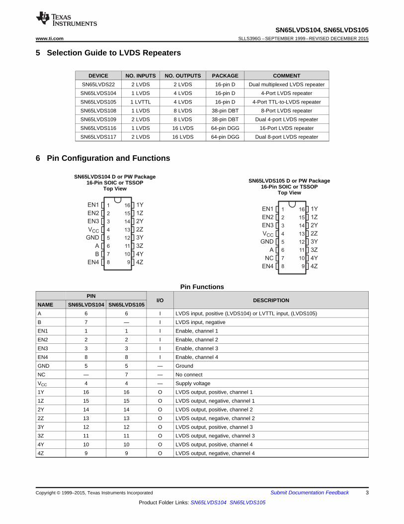
5 Selection Guide to LVDS Repeaters
DEVICE NO. INPUTS NO. OUTPUTS PACKAGE COMMENTSN65LVDS22 2 LVDS 2 LVDS 16-pin D Dual multiplexed LVDS repeater
SN65LVDS104 1 LVDS 4 LVDS 16-pin D 4-Port LVDS repeaterSN65LVDS105 1 LVTTL 4 LVDS 16-pin D 4-Port TTL-to-LVDS repeaterSN65LVDS108 1 LVDS 8 LVDS 38-pin DBT 8-Port LVDS repeaterSN65LVDS109 2 LVDS 8 LVDS 38-pin DBT Dual 4-port LVDS repeaterSN65LVDS116 1 LVDS 16 LVDS 64-pin DGG 16-Port LVDS repeaterSN65LVDS117 2 LVDS 16 LVDS 64-pin DGG Dual 8-port LVDS repeater
6 Pin Configuration and Functions
SN65LVDS104 D or PW PackageSN65LVDS105 D or PW Package16-Pin SOIC or TSSOP
16-Pin SOIC or TSSOPTop ViewTop View
Pin FunctionsPIN
I/O DESCRIPTIONNAME SN65LVDS104 SN65LVDS105A 6 6 I LVDS input, positive (LVDS104) or LVTTL input, (LVDS105)B 7 — I LVDS input, negativeEN1 1 1 I Enable, channel 1EN2 2 2 I Enable, channel 2EN3 3 3 I Enable, channel 3EN4 8 8 I Enable, channel 4GND 5 5 — GroundNC — 7 — No connectVCC 4 4 — Supply voltage1Y 16 16 O LVDS output, positive, channel 11Z 15 15 O LVDS output, negative, channel 12Y 14 14 O LVDS output, positive, channel 22Z 13 13 O LVDS output, negative, channel 23Y 12 12 O LVDS output, positive, channel 33Z 11 11 O LVDS output, negative, channel 34Y 10 10 O LVDS output, positive, channel 44Z 9 9 O LVDS output, negative, channel 4
Copyright © 1999–2015, Texas Instruments Incorporated Submit Documentation Feedback 3
Product Folder Links: SN65LVDS104 SN65LVDS105
SN65LVDS104, SN65LVDS105SLLS396G –SEPTEMBER 1999–REVISED DECEMBER 2015 www.ti.com
7 Specifications
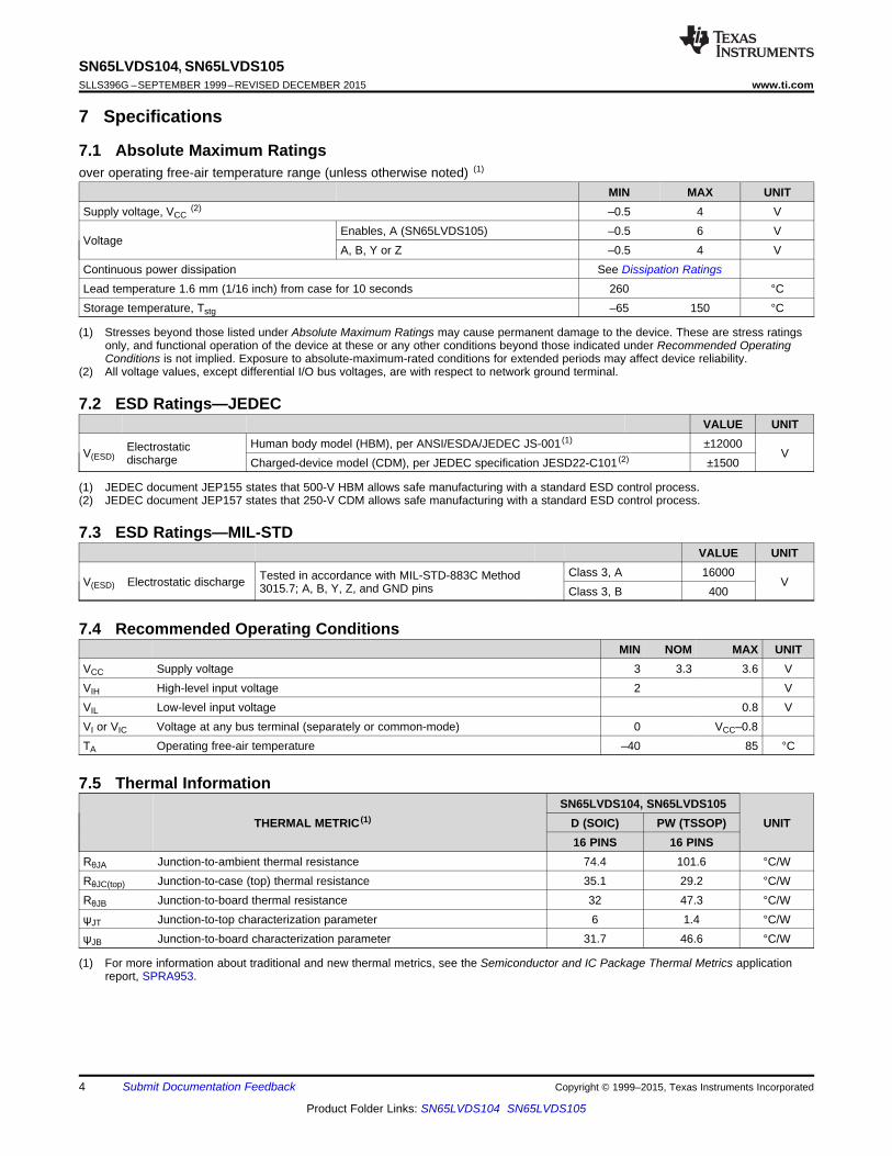
7.1 Absolute Maximum Ratingsover operating free-air temperature range (unless otherwise noted) (1)
MIN MAX UNITSupply voltage, VCC
(2) –0.5 4 VEnables, A (SN65LVDS105) –0.5 6 V
VoltageA, B, Y or Z –0.5 4 V
Continuous power dissipation See Dissipation RatingsLead temperature 1.6 mm (1/16 inch) from case for 10 seconds 260 °CStorage temperature, Tstg –65 150 °C
(1) Stresses beyond those listed under Absolute Maximum Ratings may cause permanent damage to the device. These are stress ratingsonly, and functional operation of the device at these or any other conditions beyond those indicated under Recommended OperatingConditions is not implied. Exposure to absolute-maximum-rated conditions for extended periods may affect device reliability.
(2) All voltage values, except differential I/O bus voltages, are with respect to network ground terminal.
7.2 ESD Ratings—JEDECVALUE UNIT
Human body model (HBM), per ANSI/ESDA/JEDEC JS-001 (1) ±12000ElectrostaticV(ESD) Vdischarge Charged-device model (CDM), per JEDEC specification JESD22-C101 (2) ±1500
(1) JEDEC document JEP155 states that 500-V HBM allows safe manufacturing with a standard ESD control process.(2) JEDEC document JEP157 states that 250-V CDM allows safe manufacturing with a standard ESD control process.
7.3 ESD Ratings—MIL-STDVALUE UNIT
Class 3, A 16000Tested in accordance with MIL-STD-883C MethodV(ESD) Electrostatic discharge V3015.7; A, B, Y, Z, and GND pins Class 3, B 400
7.4 Recommended Operating ConditionsMIN NOM MAX UNIT
VCC Supply voltage 3 3.3 3.6 VVIH High-level input voltage 2 VVIL Low-level input voltage 0.8 VVI or VIC Voltage at any bus terminal (separately or common-mode) 0 VCC–0.8TA Operating free-air temperature –40 85 °C
7.5 Thermal InformationSN65LVDS104, SN65LVDS105
THERMAL METRIC (1) D (SOIC) PW (TSSOP) UNIT16 PINS 16 PINS
RθJA Junction-to-ambient thermal resistance 74.4 101.6 °C/WRθJC(top) Junction-to-case (top) thermal resistance 35.1 29.2 °C/WRθJB Junction-to-board thermal resistance 32 47.3 °C/WψJT Junction-to-top characterization parameter 6 1.4 °C/WψJB Junction-to-board characterization parameter 31.7 46.6 °C/W
(1) For more information about traditional and new thermal metrics, see the Semiconductor and IC Package Thermal Metrics applicationreport, SPRA953.
4 Submit Documentation Feedback Copyright © 1999–2015, Texas Instruments Incorporated
Product Folder Links: SN65LVDS104 SN65LVDS105
SN65LVDS104, SN65LVDS105www.ti.com SLLS396G –SEPTEMBER 1999–REVISED DECEMBER 2015
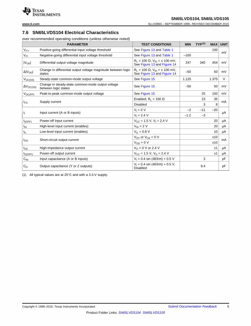
7.6 SN65LVDS104 Electrical Characteristicsover recommended operating conditions (unless otherwise noted)
PARAMETER TEST CONDITIONS MIN TYP (1) MAX UNITVIT+ Positive-going differential input voltage threshold See Figure 13 and Table 1 100
mVVIT- Negative-going differential input voltage threshold See Figure 13 and Table 1 –100
RL = 100 Ω, VID = ± 100 mV,|VOD| Differential output voltage magnitude 247 340 454 mVSee Figure 13 and Figure 14Change in differential output voltage magnitude between logic RL = 100 Ω, VID = ± 100 mV,Δ|VOD| –50 50 mVstates See Figure 13 and Figure 14
VOC(SS) Steady-state common-mode output voltage See Figure 15 1.125 1.375 VChange in steady-state common-mode output voltageΔVOC(SS) See Figure 15 –50 50 mVbetween logic states
VOC(PP) Peak-to-peak common-mode output voltage See Figure 15 25 150 mVEnabled, RL = 100 Ω 23 35
ICC Supply current mADisabled 3 8VI = 0 V –2 –11 –20
II Input current (A or B inputs) µAVI = 2.4 V –1.2 –3
II(OFF) Power-off Input current VCC = 1.5 V, VI = 2.4 V 20 µAIIH High-level input current (enables) VIH = 2 V 20 µAIIL Low-level input current (enables) VIL = 0.8 V 10 µA
VOY or VOZ = 0 V ±10IOS Short-circuit output current mA
VOD = 0 V ±10IOZ High-impedance output current VO = 0 V or 2.4 V ±1 µAIO(OFF) Power-off output current VCC = 1.5 V, VO = 2.4 V ±1 µACIN Input capacitance (A or B inputs) VI = 0.4 sin (4E6πt) + 0.5 V 3 pF
VI = 0.4 sin (4E6πt) + 0.5 V,CO Output capacitance (Y or Z outputs) 9.4 pFDisabled
(1) All typical values are at 25°C and with a 3.3-V supply.
Copyright © 1999–2015, Texas Instruments Incorporated Submit Documentation Feedback 5
Product Folder Links: SN65LVDS104 SN65LVDS105
SN65LVDS104, SN65LVDS105SLLS396G –SEPTEMBER 1999–REVISED DECEMBER 2015 www.ti.com
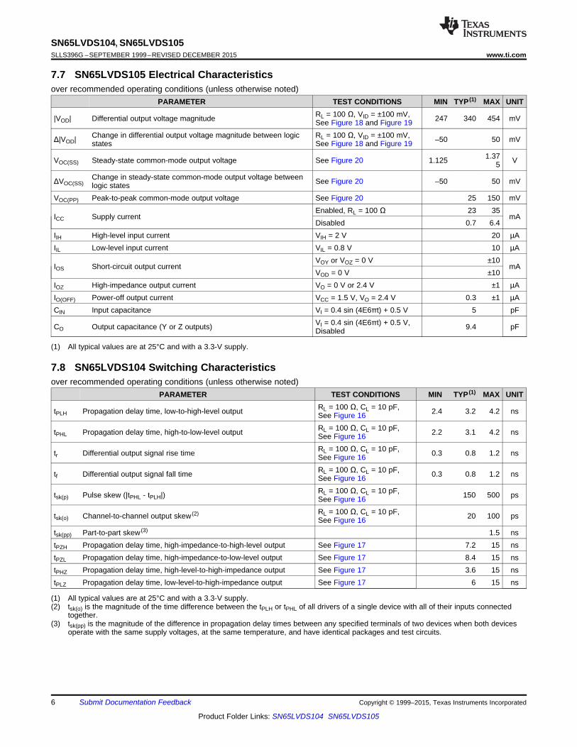
7.7 SN65LVDS105 Electrical Characteristicsover recommended operating conditions (unless otherwise noted)
PARAMETER TEST CONDITIONS MIN TYP (1) MAX UNITRL = 100 Ω, VID = ±100 mV,|VOD| Differential output voltage magnitude 247 340 454 mVSee Figure 18 and Figure 19
Change in differential output voltage magnitude between logic RL = 100 Ω, VID = ±100 mV,Δ|VOD| –50 50 mVstates See Figure 18 and Figure 191.37VOC(SS) Steady-state common-mode output voltage See Figure 20 1.125 V5
Change in steady-state common-mode output voltage betweenΔVOC(SS) See Figure 20 –50 50 mVlogic statesVOC(PP) Peak-to-peak common-mode output voltage See Figure 20 25 150 mV
Enabled, RL = 100 Ω 23 35ICC Supply current mA
Disabled 0.7 6.4IIH High-level input current VIH = 2 V 20 µAIIL Low-level input current VIL = 0.8 V 10 µA
VOY or VOZ = 0 V ±10IOS Short-circuit output current mA
VOD = 0 V ±10IOZ High-impedance output current VO = 0 V or 2.4 V ±1 µAIO(OFF) Power-off output current VCC = 1.5 V, VO = 2.4 V 0.3 ±1 µACIN Input capacitance VI = 0.4 sin (4E6πt) + 0.5 V 5 pF
VI = 0.4 sin (4E6πt) + 0.5 V,CO Output capacitance (Y or Z outputs) 9.4 pFDisabled
(1) All typical values are at 25°C and with a 3.3-V supply.
7.8 SN65LVDS104 Switching Characteristicsover recommended operating conditions (unless otherwise noted)
PARAMETER TEST CONDITIONS MIN TYP (1) MAX UNITRL = 100 Ω, CL = 10 pF,tPLH Propagation delay time, low-to-high-level output 2.4 3.2 4.2 nsSee Figure 16RL = 100 Ω, CL = 10 pF,tPHL Propagation delay time, high-to-low-level output 2.2 3.1 4.2 nsSee Figure 16RL = 100 Ω, CL = 10 pF,tr Differential output signal rise time 0.3 0.8 1.2 nsSee Figure 16RL = 100 Ω, CL = 10 pF,tf Differential output signal fall time 0.3 0.8 1.2 nsSee Figure 16RL = 100 Ω, CL = 10 pF,tsk(p) Pulse skew (|tPHL - tPLH|) 150 500 psSee Figure 16RL = 100 Ω, CL = 10 pF,tsk(o) Channel-to-channel output skew (2) 20 100 psSee Figure 16
tsk(pp) Part-to-part skew (3) 1.5 nstPZH Propagation delay time, high-impedance-to-high-level output See Figure 17 7.2 15 nstPZL Propagation delay time, high-impedance-to-low-level output See Figure 17 8.4 15 nstPHZ Propagation delay time, high-level-to-high-impedance output See Figure 17 3.6 15 nstPLZ Propagation delay time, low-level-to-high-impedance output See Figure 17 6 15 ns
(1) All typical values are at 25°C and with a 3.3-V supply.(2) tsk(o) is the magnitude of the time difference between the tPLH or tPHL of all drivers of a single device with all of their inputs connected
together.(3) tsk(pp) is the magnitude of the difference in propagation delay times between any specified terminals of two devices when both devices
operate with the same supply voltages, at the same temperature, and have identical packages and test circuits.
6 Submit Documentation Feedback Copyright © 1999–2015, Texas Instruments Incorporated
Product Folder Links: SN65LVDS104 SN65LVDS105
SN65LVDS104, SN65LVDS105www.ti.com SLLS396G –SEPTEMBER 1999–REVISED DECEMBER 2015
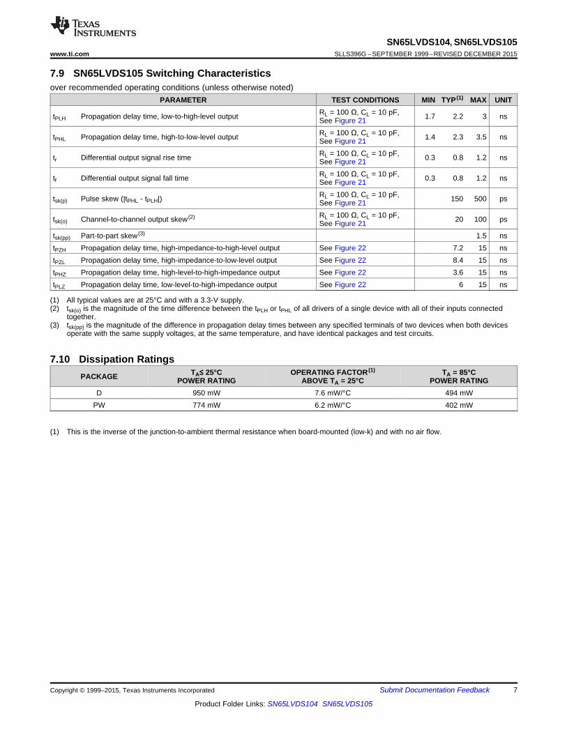
7.9 SN65LVDS105 Switching Characteristicsover recommended operating conditions (unless otherwise noted)
PARAMETER TEST CONDITIONS MIN TYP (1) MAX UNITRL = 100 Ω, CL = 10 pF,tPLH Propagation delay time, low-to-high-level output 1.7 2.2 3 nsSee Figure 21RL = 100 Ω, CL = 10 pF,tPHL Propagation delay time, high-to-low-level output 1.4 2.3 3.5 nsSee Figure 21RL = 100 Ω, CL = 10 pF,tr Differential output signal rise time 0.3 0.8 1.2 nsSee Figure 21RL = 100 Ω, CL = 10 pF,tf Differential output signal fall time 0.3 0.8 1.2 nsSee Figure 21RL = 100 Ω, CL = 10 pF,tsk(p) Pulse skew (|tPHL - tPLH|) 150 500 psSee Figure 21RL = 100 Ω, CL = 10 pF,tsk(o) Channel-to-channel output skew (2) 20 100 psSee Figure 21
tsk(pp) Part-to-part skew (3) 1.5 nstPZH Propagation delay time, high-impedance-to-high-level output See Figure 22 7.2 15 nstPZL Propagation delay time, high-impedance-to-low-level output See Figure 22 8.4 15 nstPHZ Propagation delay time, high-level-to-high-impedance output See Figure 22 3.6 15 nstPLZ Propagation delay time, low-level-to-high-impedance output See Figure 22 6 15 ns
(1) All typical values are at 25°C and with a 3.3-V supply.(2) tsk(o) is the magnitude of the time difference between the tPLH or tPHL of all drivers of a single device with all of their inputs connected
together.(3) tsk(pp) is the magnitude of the difference in propagation delay times between any specified terminals of two devices when both devices
operate with the same supply voltages, at the same temperature, and have identical packages and test circuits.
7.10 Dissipation RatingsTA≤ 25°C OPERATING FACTOR (1) TA = 85°CPACKAGE POWER RATING ABOVE TA = 25°C POWER RATING
D 950 mW 7.6 mW/°C 494 mWPW 774 mW 6.2 mW/°C 402 mW
(1) This is the inverse of the junction-to-ambient thermal resistance when board-mounted (low-k) and with no air flow.
Copyright © 1999–2015, Texas Instruments Incorporated Submit Documentation Feedback 7
Product Folder Links: SN65LVDS104 SN65LVDS105
TA − Free-Air T emperature − °C
2.8
2.9
3.0
3.1
3.2
3.3
3.4
3.5
3.6
−50 −25 0 25 50 75 100
tP
LH−
Low
-To-
Hig
h P
ropa
gatio
n D
elay
Tim
e −
ns
VCC = 3.6 V
VCC = 3 V
VCC = 3.3 V
TA − Free-Air T emperature − °C
2.8
2.9
3.0
3.1
3.2
3.3
3.4
3.5
3.6
−50 −25 0 25 50 75 100
tP
HL
− H
igh-
To-
Low
Pro
paga
tion
Del
ay T
ime
− ns
VCC = 3.6 V
VCC = 3 V
VCC = 3.3 V
0
IOL − Low-Level Output Current − mA
4
3
04 6
2
2
VCC = 3.3 VTA = 25°C
1
VO
L−
Low
-Lev
el O
utpu
t Vol
tage
− V
−4
IOH − High-Level Output Current − mA
3.5
2.5
0−2 0
1.5
−3
0.5VO
H−
Hig
h-Le
vel O
utpu
t Vol
tage
− V
−1
3
2
1
VCC = 3.3 VTA = 25°C
25
30
35
40
45
50
55
60
50 100 150 200 250 300 350
f − Frequency − MHz
− S
uppl
y C
urre
nt −
mA
IC
C
VCC = 3.6 V
VCC = 3 V
All Outputs Loadedand Enabled
VCC = 3.3 V
20
25
30
35
40
45
50
50 100 150 200 250 300 350
f − Frequency − MHz
− S
uppl
y C
urre
nt −
mA
IC
C
VCC = 3.6 V
VCC = 3 V
All Outputs Loadedand Enabled
VCC = 3.3 V
SN65LVDS104, SN65LVDS105SLLS396G –SEPTEMBER 1999–REVISED DECEMBER 2015 www.ti.com
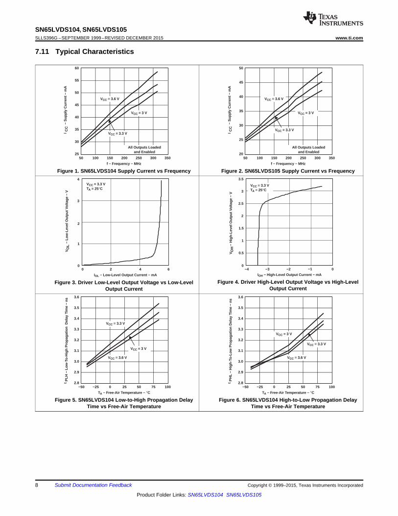
7.11 Typical Characteristics
Figure 1. SN65LVDS104 Supply Current vs Frequency Figure 2. SN65LVDS105 Supply Current vs Frequency
Figure 4. Driver High-Level Output Voltage vs High-LevelFigure 3. Driver Low-Level Output Voltage vs Low-LevelOutput CurrentOutput Current
Figure 5. SN65LVDS104 Low-to-High Propagation Delay Figure 6. SN65LVDS104 High-to-Low Propagation DelayTime vs Free-Air Temperature Time vs Free-Air Temperature
8 Submit Documentation Feedback Copyright © 1999–2015, Texas Instruments Incorporated
Product Folder Links: SN65LVDS104 SN65LVDS105
0
2
4
6
8
10
12
14
0 100 200 300 400 500 600Clock Frequency − MHz
Pea
k-to
-Pea
k Ji
tter −
ps
TA = 25C
VCC = 3 V
VCC = 3.6 V
0
100
200
300
400
500
600
0 100 200 300 400 500 600
Signaling Rate − Mbps
VCC = 3.6 V
VCC = 3 V
Pea
k-to
-Pea
k Ji
tter −
ps
TA = 25C
0
100
200
300
400
500
600
700
800
0 100 200 300 400 500 600
Signaling Rate − Mbps
VCC = 3.6 V
VCC = 3 V
Pea
k-to
-Pea
k Ji
tter −
ps
TA = 25C
0
2
4
6
8
10
12
14
16
18
0 100 200 300 400 500 600Clock Frequency − MHz
Pea
k-to
-Pea
k Ji
tter −
ps
TA = 25C
VCC = 3 V
VCC = 3.6 V
TA − Free-Air T emperature − °C
2.0
2.1
2.2
2.3
2.4
2.5
2.6
2.7
−50 −25 0 25 50 75 100
tP
LH−
Low
-To-
Hig
h P
ropa
gatio
n D
elay
Tim
e −
ns
VCC = 3.6 V
VCC = 3 V
VCC = 3.3 V
TA − Free-Air T emperature − °C
2.0
2.1
2.2
2.3
2.4
2.5
2.6
2.7
−50 −25 0 25 50 75 100
tP
HL
− H
igh-
To-
Low
Pro
paga
tion
Del
ay T
ime
− ns
VCC = 3.6 V
VCC = 3 V
VCC = 3.3 V
SN65LVDS104, SN65LVDS105www.ti.com SLLS396G –SEPTEMBER 1999–REVISED DECEMBER 2015
Typical Characteristics (continued)
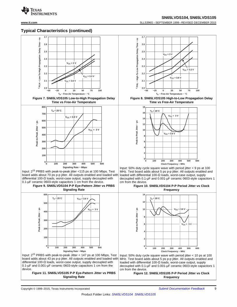
Figure 7. SN65LVDS105 Low-to-High Propagation Delay Figure 8. SN65LVDS105 High-to-Low Propagation DelayTime vs Free-Air Temperature Time vs Free-Air Temperature
Input: 50% duty cycle square wave with period jitter < 9 ps at 100Input: 215 PRBS with peak-to-peak jitter <115 ps at 100 Mbps. Test MHz. Test board adds about 5 ps p-p jitter. All outputs enabled andboard adds about 70 ps p-p jitter. All outputs enabled and loaded with loaded with differential 100-Ω loads, worst-case output, supplydifferential 100-Ω loads, worst-case output, supply decoupled with decoupled with 0.1-µF and 0.001-µF ceramic 0603-style capacitors 10.1-µF ceramic 0603-style capacitors 1 cm from the device. cm from the device.
Figure 9. SN65LVDS104 P-P Eye-Pattern Jitter vs PRBS Figure 10. SN65LVDS104 P-P Period Jitter vs ClockSignaling Rate Frequency
Input: 215 PRBS with peak-to-peak Jitter < 147 ps at 100 Mbps, Test Input: 50% duty cycle square wave with period jitter < 10 ps at 100board adds about 43 ps p-p jitter. All outputs enabled and loaded with MHz. Test board adds about 5 ps p-p jitter. All outputs enabled anddifferential 100-Ω loads, worst-case output, supply decoupled with loaded with differential 100-Ω loads, worst-case output, supply0.1-µF and 0.001-µF ceramic 0603-style capacitors 1 cm from the decoupled with 0.1-µF and 0.001-µF ceramic 0603-style capacitors 1device. cm from the device.
Figure 11. SN65LVDS105 P-P Eye-Pattern Jitter vs PRBS Figure 12. SN65LVDS105 P-P Period Jitter vs ClockSignaling Rate Frequency
Copyright © 1999–2015, Texas Instruments Incorporated Submit Documentation Feedback 9
Product Folder Links: SN65LVDS104 SN65LVDS105
±
3.75 kΩ
0 V ≤ VTEST ≤ 2.4 V
Y
ZVODInput 100 Ω
3.75 kΩ
II
VIB
VID
VIA
A
B
IIBVOD
VOZ
VOY
VOC
IOY
IOZZ
Y
VOYVOZ2
SN65LVDS104, SN65LVDS105SLLS396G –SEPTEMBER 1999–REVISED DECEMBER 2015 www.ti.com
8 Parameter Measurement Information
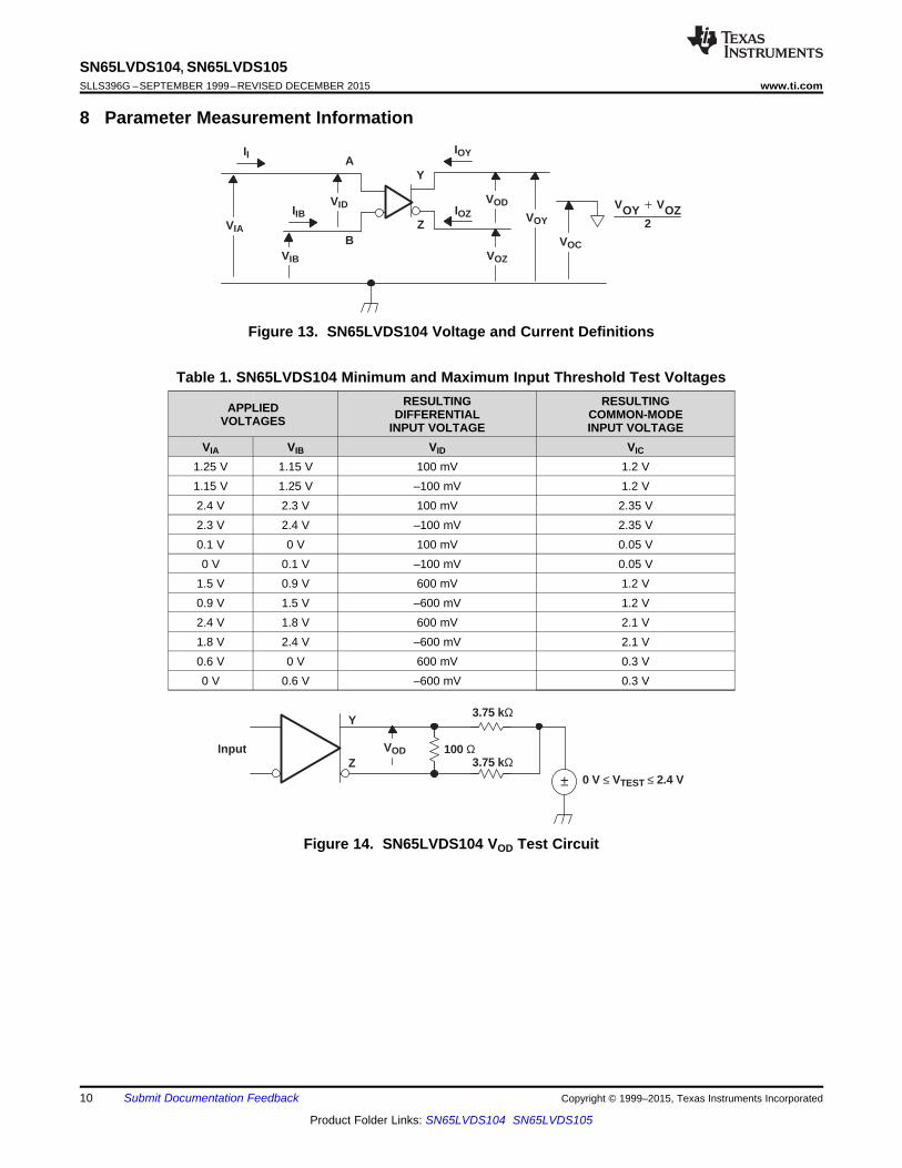
Figure 13. SN65LVDS104 Voltage and Current Definitions
Table 1. SN65LVDS104 Minimum and Maximum Input Threshold Test VoltagesRESULTING RESULTINGAPPLIED DIFFERENTIAL COMMON-MODEVOLTAGES INPUT VOLTAGE INPUT VOLTAGE
VIA VIB VID VIC
1.25 V 1.15 V 100 mV 1.2 V1.15 V 1.25 V –100 mV 1.2 V2.4 V 2.3 V 100 mV 2.35 V2.3 V 2.4 V –100 mV 2.35 V0.1 V 0 V 100 mV 0.05 V0 V 0.1 V –100 mV 0.05 V
1.5 V 0.9 V 600 mV 1.2 V0.9 V 1.5 V –600 mV 1.2 V2.4 V 1.8 V 600 mV 2.1 V1.8 V 2.4 V –600 mV 2.1 V0.6 V 0 V 600 mV 0.3 V0 V 0.6 V –600 mV 0.3 V
Figure 14. SN65LVDS104 VOD Test Circuit
10 Submit Documentation Feedback Copyright © 1999–2015, Texas Instruments Incorporated
Product Folder Links: SN65LVDS104 SN65LVDS105
1.4 V1.2 V1 V
tPLH tPHL
100%80%
20%0%
Input
Output
0 V
tf tr
VOD(H)
VOD(L)
VIB
VIA
Y
ZVOD 100 Ω ± 1%
AInput
(see Note A)
CL = 10 pF(2 Places)(see Note B)
B
Y
Z
49.9 Ω ± 1% (2 Places)
VOC
VO
VOC(PP)VOC(SS)
1 V
1.4 V
VIInput(see Note A)
VI
CL = 10 pF(2 Places)(see Note B)
SN65LVDS104, SN65LVDS105www.ti.com SLLS396G –SEPTEMBER 1999–REVISED DECEMBER 2015
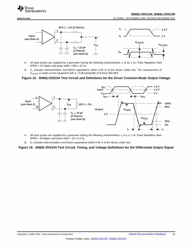
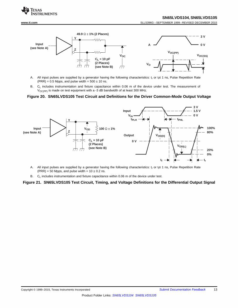
A. All input pulses are supplied by a generator having the following characteristics: tr or tf≤ 1 ns, Pulse Repetition Rate(PRR) = 0.5 Mpps, and pulse width = 500 ± 10 ns.
B. CL includes instrumentation and fixture capacitance within 0.06 m of the device under test. The measurement ofVOC(PP) is made on test equipment with a –3 dB bandwidth of at least 300 MHz.
Figure 15. SN65LVDS104 Test Circuit and Definitions for the Driver Common-Mode Output Voltage
A. All input pulses are supplied by a generator having the following characteristics: tr or tf ≤ 1 ns, Pulse Repetition Rate(PRR) = 50 Mpps, and pulse width = 10 ± 0.2 ns.
B. CL includes instrumentation and fixture capacitance within 0.06 m of the device under test.
Figure 16. SN65LVDS104 Test Circuit, Timing, and Voltage Definitions for the Differential Output Signal
Copyright © 1999–2015, Texas Instruments Incorporated Submit Documentation Feedback 11
Product Folder Links: SN65LVDS104 SN65LVDS105
±
3.75 kΩ
0 V ≤ VTEST ≤ 2.4 V
Y
ZVODInput 100 Ω
3.75 kΩ
II
VIA
A VOD
VOZ
VOY
VOC
IOY
IOZZ
Y
VOYVOZ2
tPZH tPHZ
tPZL tPLZ
3 V1.5 V0 V
≅ 1.4 V1.25 V1.2 V
≅ 1 V
1.2 V1.15 V
EN
VOY or VOZ
VOZ or VOY
Y
Z
CL = 10 pF(2 Places)
(see Note B)
49.9 Ω ± 1% (2 Places)
1.2 V
VOY VOZ
1 V or 1.4 V
1.2 V
EN
Input(see Note A)
SN65LVDS104, SN65LVDS105SLLS396G –SEPTEMBER 1999–REVISED DECEMBER 2015 www.ti.com
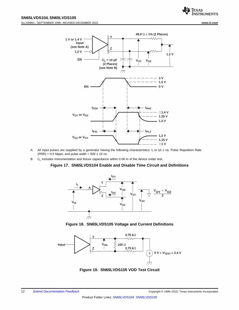
A. All input pulses are supplied by a generator having the following characteristics: tr or tf≤ 1 ns, Pulse Repetition Rate(PRR) = 0.5 Mpps, and pulse width = 500 ± 10 ns.
B. CL includes instrumentation and fixture capacitance within 0.06 m of the device under test.
Figure 17. SN65LVDS104 Enable and Disable Time Circuit and Definitions
Figure 18. SN65LVDS105 Voltage and Current Definitions
Figure 19. SN65LVDS105 VOD Test Circuit
12 Submit Documentation Feedback Copyright © 1999–2015, Texas Instruments Incorporated
Product Folder Links: SN65LVDS104 SN65LVDS105
Y
ZVODInput
(see Note A)
CL = 10 pF(2 Places)(see Note B)
100 Ω ± 1%
3 V1.5 V0 V
tPLH tPHL
100%80%
20%0%
Input
Output
0 V
tf tr
VOD(H)
VOD(L)
VIA
Y
Z
49.9 Ω ± 1% (2 Places)
VOC
VO
VOC(PP)VOC(SS)
0 VA
3 V
CL = 10 pF(2 Places)(see Note B)
Input(see Note A)
SN65LVDS104, SN65LVDS105www.ti.com SLLS396G –SEPTEMBER 1999–REVISED DECEMBER 2015
A. All input pulses are supplied by a generator having the following characteristics: tr or tf≤ 1 ns, Pulse Repetition Rate(PRR) = 0.5 Mpps, and pulse width = 500 ± 10 ns.
B. CL includes instrumentation and fixture capacitance within 0.06 m of the device under test. The measurement ofVOC(PP) is made on test equipment with a -3 dB bandwidth of at least 300 MHz.
Figure 20. SN65LVDS105 Test Circuit and Definitions for the Driver Common-Mode Output Voltage
A. All input pulses are supplied by a generator having the following characteristics: tr or tf≤ 1 ns, Pulse Repetition Rate(PRR) = 50 Mpps, and pulse width = 10 ± 0.2 ns.
B. CL includes instrumentation and fixture capacitance within 0.06 m of the device under test.
Figure 21. SN65LVDS105 Test Circuit, Timing, and Voltage Definitions for the Differential Output Signal
Copyright © 1999–2015, Texas Instruments Incorporated Submit Documentation Feedback 13
Product Folder Links: SN65LVDS104 SN65LVDS105
tPZH tPHZ
tPZL tPLZ
3 V1.5 V0 V
≅ 1.4 V1.25 V1.2 V
≅ 1 V
1.2 V1.15 V
EN
VOYor
VOZ
VOZor
VOY
Y
Z
CL = 10 pF(2 Places)
(see Note B)
49.9 Ω ± 1% (2 Places)
1.2 V
VOY VOZ
0.8 V or 2 V
EN
Input(see Note A)
SN65LVDS104, SN65LVDS105SLLS396G –SEPTEMBER 1999–REVISED DECEMBER 2015 www.ti.com
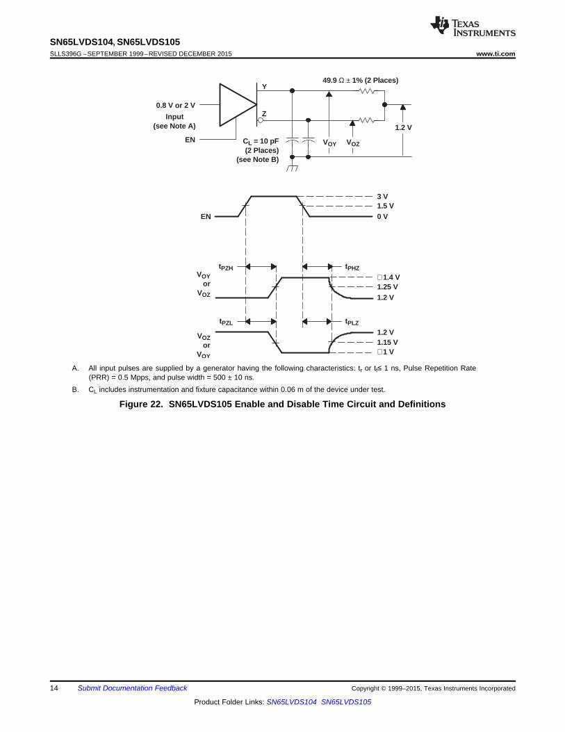
A. All input pulses are supplied by a generator having the following characteristics: tr or tf≤ 1 ns, Pulse Repetition Rate(PRR) = 0.5 Mpps, and pulse width = 500 ± 10 ns.
B. CL includes instrumentation and fixture capacitance within 0.06 m of the device under test.
Figure 22. SN65LVDS105 Enable and Disable Time Circuit and Definitions
14 Submit Documentation Feedback Copyright © 1999–2015, Texas Instruments Incorporated
Product Folder Links: SN65LVDS104 SN65LVDS105
4Z
4Y
3Z
3Y
2Z
2Y
1Z
1Y
EN1
EN2
A
EN4
EN3
4Z
4Y
3Z
3Y
2Z
2Y
1Z
1Y
EN1
EN2
A
EN4
EN3
B
SN65LVDS104, SN65LVDS105www.ti.com SLLS396G –SEPTEMBER 1999–REVISED DECEMBER 2015
9 Detailed Description
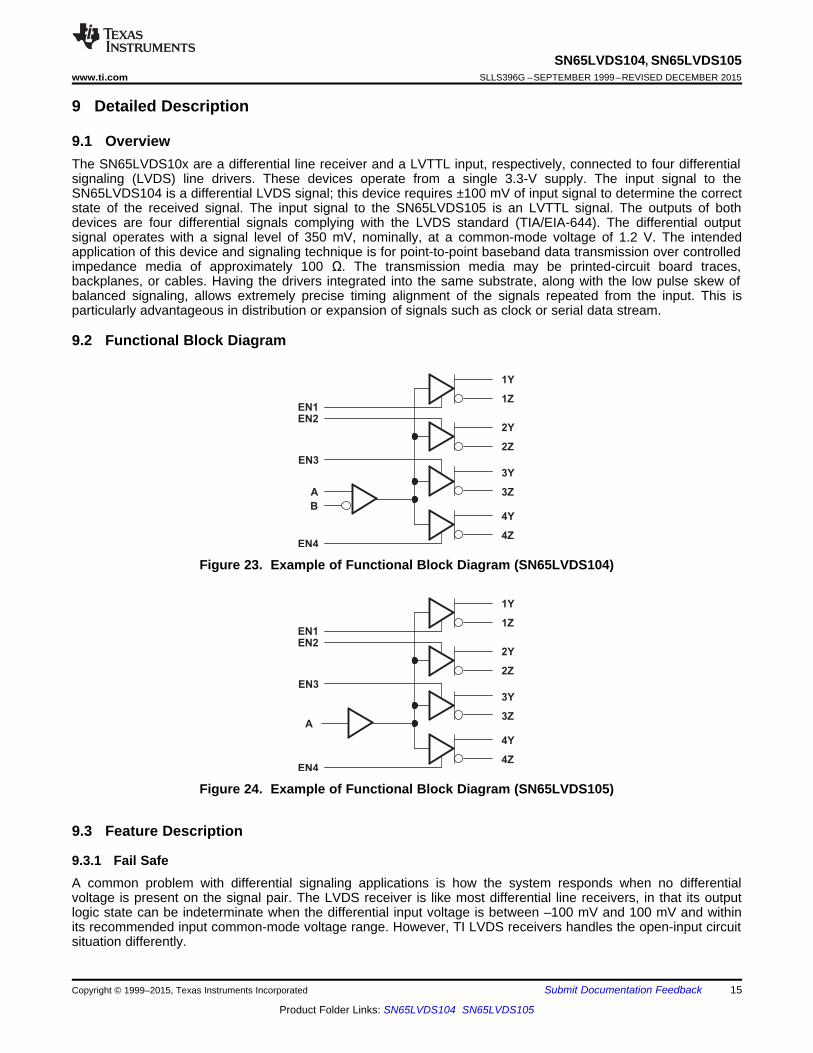
9.1 OverviewThe SN65LVDS10x are a differential line receiver and a LVTTL input, respectively, connected to four differentialsignaling (LVDS) line drivers. These devices operate from a single 3.3-V supply. The input signal to theSN65LVDS104 is a differential LVDS signal; this device requires ±100 mV of input signal to determine the correctstate of the received signal. The input signal to the SN65LVDS105 is an LVTTL signal. The outputs of bothdevices are four differential signals complying with the LVDS standard (TIA/EIA-644). The differential outputsignal operates with a signal level of 350 mV, nominally, at a common-mode voltage of 1.2 V. The intendedapplication of this device and signaling technique is for point-to-point baseband data transmission over controlledimpedance media of approximately 100 Ω. The transmission media may be printed-circuit board traces,backplanes, or cables. Having the drivers integrated into the same substrate, along with the low pulse skew ofbalanced signaling, allows extremely precise timing alignment of the signals repeated from the input. This isparticularly advantageous in distribution or expansion of signals such as clock or serial data stream.
9.2 Functional Block Diagram
Figure 23. Example of Functional Block Diagram (SN65LVDS104)
Figure 24. Example of Functional Block Diagram (SN65LVDS105)
9.3 Feature Description
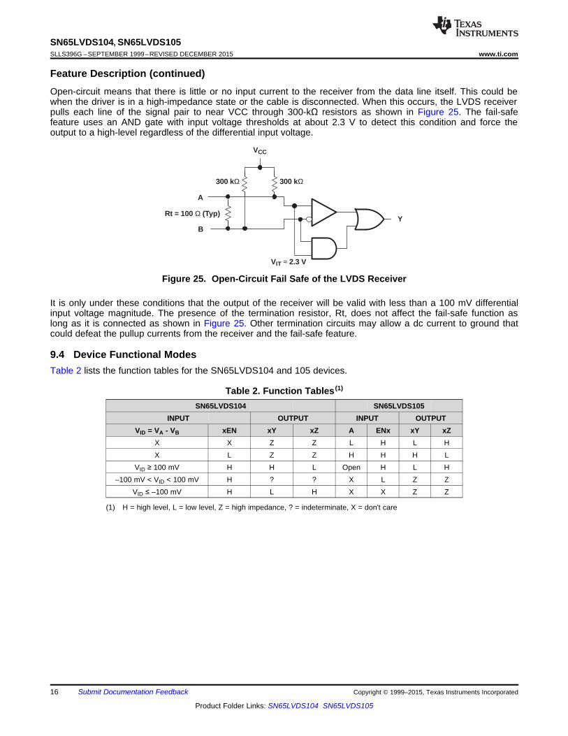
9.3.1 Fail SafeA common problem with differential signaling applications is how the system responds when no differentialvoltage is present on the signal pair. The LVDS receiver is like most differential line receivers, in that its outputlogic state can be indeterminate when the differential input voltage is between –100 mV and 100 mV and withinits recommended input common-mode voltage range. However, TI LVDS receivers handles the open-input circuitsituation differently.
Copyright © 1999–2015, Texas Instruments Incorporated Submit Documentation Feedback 15
Product Folder Links: SN65LVDS104 SN65LVDS105
Rt = 100 Ω (Typ)
300 kΩ 300 kΩ
VCC
VIT ≈ 2.3 V
A
BY
SN65LVDS104, SN65LVDS105SLLS396G –SEPTEMBER 1999–REVISED DECEMBER 2015 www.ti.com
Feature Description (continued)Open-circuit means that there is little or no input current to the receiver from the data line itself. This could bewhen the driver is in a high-impedance state or the cable is disconnected. When this occurs, the LVDS receiverpulls each line of the signal pair to near VCC through 300-kΩ resistors as shown in Figure 25. The fail-safefeature uses an AND gate with input voltage thresholds at about 2.3 V to detect this condition and force theoutput to a high-level regardless of the differential input voltage.
Figure 25. Open-Circuit Fail Safe of the LVDS Receiver
It is only under these conditions that the output of the receiver will be valid with less than a 100 mV differentialinput voltage magnitude. The presence of the termination resistor, Rt, does not affect the fail-safe function aslong as it is connected as shown in Figure 25. Other termination circuits may allow a dc current to ground thatcould defeat the pullup currents from the receiver and the fail-safe feature.
9.4 Device Functional ModesTable 2 lists the function tables for the SN65LVDS104 and 105 devices.
Table 2. Function Tables (1)
SN65LVDS104 SN65LVDS105INPUT OUTPUT INPUT OUTPUT
VID = VA - VB xEN xY xZ A ENx xY xZX X Z Z L H L HX L Z Z H H H L
VID ≥ 100 mV H H L Open H L H–100 mV < VID < 100 mV H ? ? X L Z Z
VID ≤ –100 mV H L H X X Z Z
(1) H = high level, L = low level, Z = high impedance, ? = indeterminate, X = don't care
16 Submit Documentation Feedback Copyright © 1999–2015, Texas Instruments Incorporated
Product Folder Links: SN65LVDS104 SN65LVDS105
VDD
50 Ω
50 Ω
A
B1.35 V < VTT < 1.65 V
0.1 µF LVDS Receiver
VDD
50 Ω25 Ω
50Ω
A
B1/2 VDD
0.1 µF LVDS Receiver
300 kΩ300 kΩ
VCC
7 V 7 V
AInput
BInput
7 V
300 kΩ
50 Ω
VCC
EN and A (’LVDS105)
Input
VCC
5 Ω
7 V
Y or ZOutput
10 kΩ
SN65LVDS104, SN65LVDS105www.ti.com SLLS396G –SEPTEMBER 1999–REVISED DECEMBER 2015
Figure 26. Equivalent Input and Output Schematic Diagrams
9.4.1 Input Level TranslationAn LVDS receiver can be used to receive various other types of logic signals. Figure 27 through Figure 36 showthe termination circuits for SSTL, HSTL, GTL, BTL, LVPECL, PECL, CMOS, and TTL.
Figure 27. Sub-Series Terminated (SSTL) or High-Speed Transceiver Logic (HSTL)
Figure 28. Center Tap Termination
Copyright © 1999–2015, Texas Instruments Incorporated Submit Documentation Feedback 17
Product Folder Links: SN65LVDS104 SN65LVDS105
3.3 V
33 Ω
A
B
3.3 V
LVDS Receiver
33 Ω
51 Ω
ECL
50 Ω
50 Ω
51 Ω
120 Ω120 Ω
A
B1.47 V < VTT < 1.62 V
0.1 µF LVDS Receiver
Z0 Z0
VDD
A
B
1.14 V < VTT < 1.26 V
LVDS Receiver2 kΩ
50 Ω
0.1 µF
50 Ω1 kΩ
SN65LVDS104, SN65LVDS105SLLS396G –SEPTEMBER 1999–REVISED DECEMBER 2015 www.ti.com
Figure 29. Gunning Transceiver Logic (GTL)
Figure 30. Backplane Transceiver
Figure 31. Low-Voltage Positive Emitter-Coupled Logic (LVPECL)
18 Submit Documentation Feedback Copyright © 1999–2015, Texas Instruments Incorporated
Product Folder Links: SN65LVDS104 SN65LVDS105
5 V
A
B
5 V
LVDS Receiver3.32 kΩ 0.1 µF
10 kΩ
560 Ω
560 Ω
3.3 V
A
B
3.3 V
LVDS Receiver7.5 kΩ 0.1 µF
7.5 kΩ
5 V
100 Ω
A
B
5 V
LVDS Receiver
100 Ω
33 Ω
ECL
50 Ω
50 Ω
33 Ω
82 Ω82 Ω
SN65LVDS104, SN65LVDS105www.ti.com SLLS396G –SEPTEMBER 1999–REVISED DECEMBER 2015
Figure 32. Positive Emitter-Coupled Logic (PECL)
Figure 33. 3.3-V CMOS
Figure 34. 5-V CMOS
Copyright © 1999–2015, Texas Instruments Incorporated Submit Documentation Feedback 19
Product Folder Links: SN65LVDS104 SN65LVDS105
3.3 V
A
B
3.3 V
LVDS Receiver3.01 kΩ 0.1 µF
4.02 kΩ
560 Ω
5 V
A
B
5 V
LVDS Receiver4.02 kΩ 0.1 µF
10 kΩ
470 Ω
3.3 V
SN65LVDS104, SN65LVDS105SLLS396G –SEPTEMBER 1999–REVISED DECEMBER 2015 www.ti.com
Figure 35. 5-V TTL
Figure 36. LVTTL
20 Submit Documentation Feedback Copyright © 1999–2015, Texas Instruments Incorporated
Product Folder Links: SN65LVDS104 SN65LVDS105
Driver 100Ω Receiver
IN+
IN-
OUT+
OUT-
14
SN65LVDS104, SN65LVDS105www.ti.com SLLS396G –SEPTEMBER 1999–REVISED DECEMBER 2015
10 Application and Implementation
NOTEInformation in the following applications sections is not part of the TI componentspecification, and TI does not warrant its accuracy or completeness. TI’s customers areresponsible for determining suitability of components for their purposes. Customers shouldvalidate and test their design implementation to confirm system functionality.
10.1 Application InformationThe SN65LVDS049 is a dual LVDS driver-receiver pair. The functionality of these devices is simple, yetextremely flexible, leading to their use in designs ranging from wireless base stations to desktop computers. Thevaried class of potential applications share features and applications discussed in the paragraphs below.
10.2 Typical Application
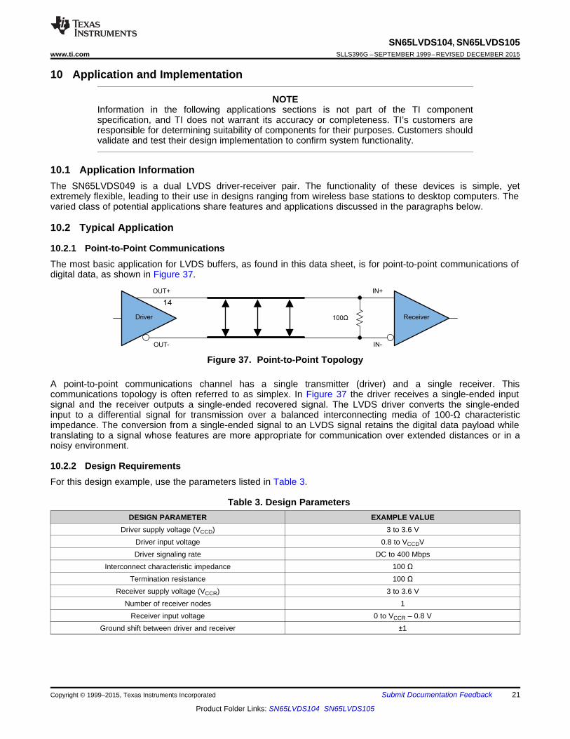
10.2.1 Point-to-Point CommunicationsThe most basic application for LVDS buffers, as found in this data sheet, is for point-to-point communications ofdigital data, as shown in Figure 37.
Figure 37. Point-to-Point Topology
A point-to-point communications channel has a single transmitter (driver) and a single receiver. Thiscommunications topology is often referred to as simplex. In Figure 37 the driver receives a single-ended inputsignal and the receiver outputs a single-ended recovered signal. The LVDS driver converts the single-endedinput to a differential signal for transmission over a balanced interconnecting media of 100-Ω characteristicimpedance. The conversion from a single-ended signal to an LVDS signal retains the digital data payload whiletranslating to a signal whose features are more appropriate for communication over extended distances or in anoisy environment.
10.2.2 Design RequirementsFor this design example, use the parameters listed in Table 3.
Table 3. Design ParametersDESIGN PARAMETER EXAMPLE VALUE
Driver supply voltage (VCCD) 3 to 3.6 VDriver input voltage 0.8 to VCCDVDriver signaling rate DC to 400 Mbps
Interconnect characteristic impedance 100 ΩTermination resistance 100 Ω
Receiver supply voltage (VCCR) 3 to 3.6 VNumber of receiver nodes 1
Receiver input voltage 0 to VCCR – 0.8 VGround shift between driver and receiver ±1
Copyright © 1999–2015, Texas Instruments Incorporated Submit Documentation Feedback 21
Product Folder Links: SN65LVDS104 SN65LVDS105
0.004 µF0.1 µF
3.3 V
LVDS
100 mAC 4 ns = 0.004 F
0.1V
æ ö= ´ mç ÷
è ø
Maximum Step Change Supply Currentchip Rise Time
Maximum Power Supply Noise
IC T
V
Dæ ö= ´ç ÷Dè ø
SN65LVDS104, SN65LVDS105SLLS396G –SEPTEMBER 1999–REVISED DECEMBER 2015 www.ti.com
Typical Application (continued)10.2.3 Detailed Design Procedure
10.2.3.1 Bypass CapacitanceBypass capacitors play a key role in power distribution circuitry. At low frequencies, power supply offers very low-impedance paths between the terminals. However, as higher frequency currents propagate through powertraces, the source is quite often incapable of maintaining a low-impedance path to ground. Bypass capacitors areused to address this shortcoming. Usually, large bypass capacitors (10 μF to 1000 μF) at the board level do agood job into the kHz range. Due to their size and length of their leads, large capacitors tend to have largeinductance values at the switching frequencies. To solve this problem, smaller capacitors must be (nF to μFrange) installed locally next to the integrated circuit.
Multilayer ceramic chip or surface-mount capacitors (size 0603 or 0805) minimize lead inductances of bypasscapacitors in high-speed environments, because their lead inductance is about 1 nH. For comparison purposes,a typical capacitor with leads has a lead inductance of approximately 5 nH.
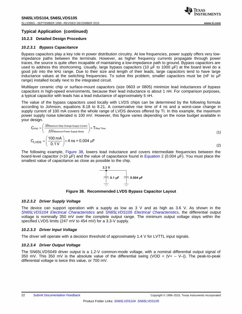
The value of the bypass capacitors used locally with LVDS chips can be determined by the following formulaaccording to Johnson, equations 8.18 to 8.21. A conservative rise time of 4 ns and a worst-case change insupply current of 100 mA covers the whole range of LVDS devices offered by TI. In this example, the maximumpower supply noise tolerated is 100 mV. However, this figure varies depending on the noise budget available inyour design.
(1)
(2)
The following example, Figure 38, lowers lead inductance and covers intermediate frequencies between theboard-level capacitor (>10 μF) and the value of capacitance found in Equation 2 (0.004 μF). You must place thesmallest value of capacitance as close as possible to the chip.
Figure 38. Recommended LVDS Bypass Capacitor Layout
10.2.3.2 Driver Supply VoltageThe device can support operation with a supply as low as 3 V and as high as 3.6 V. As shown in theSN65LVDS104 Electrical Characteristics and SN65LVDS105 Electrical Characteristics, the differential outputvoltage is nominally 350 mV over the complete output range. The minimum output voltage stays within thespecified LVDS limits (247 mV to 454 mV) for a 3.3-V supply.
10.2.3.3 Driver Input VoltageThe driver will operate with a decision threshold of approximately 1.4 V for LVTTL input signals.
10.2.3.4 Driver Output VoltageThe SN65LVDS049 driver output is a 1.2-V common-mode voltage, with a nominal differential output signal of350 mV. This 350 mV is the absolute value of the differential swing (VOD = |V+ – V–|). The peak-to-peakdifferential voltage is twice this value, or 700 mV.
22 Submit Documentation Feedback Copyright © 1999–2015, Texas Instruments Incorporated
Product Folder Links: SN65LVDS104 SN65LVDS105
SN65LVDS104, SN65LVDS105www.ti.com SLLS396G –SEPTEMBER 1999–REVISED DECEMBER 2015
Typical Application (continued)10.2.3.5 Interconnecting MediaThe physical communication channel between the driver and the receiver may be any balanced paired metalconductors meeting the requirements of the LVDS standard. This media may be a twisted-pair, twinax, flat ribboncable, or PCB traces. The nominal characteristic impedance of the interconnect must be from 100 Ω to 120 Ωwith variation no more than 10% (90 Ω to 132 Ω).
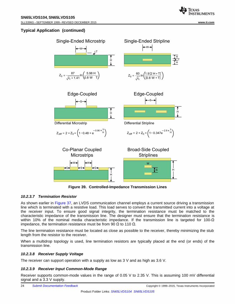
10.2.3.6 PCB Transmission LinesAs per SNLA187, Figure 39 depicts several transmission line structures commonly used in PCBs. Each structureconsists of a signal line and a return path with uniform cross-section along its length. A microstrip is a signaltrace on the top (or bottom) layer, separated by a dielectric layer from its return path in a ground or power plane.A stripline is a signal trace in the inner layer, with a dielectric layer in between a ground plane above and belowthe signal trace. The dimensions of the structure along with the dielectric material properties determine thecharacteristic impedance of the transmission line (also called controlled-impedance transmission line).
When two signal lines are placed near one another, they form a pair of coupled transmission lines. Figure 39shows examples of edge-coupled microstrips, and edge-coupled or broad-side-coupled striplines. When excitedby differential signals, the coupled transmission line is referred to as a differential pair. The characteristicimpedance of each line is called odd-mode impedance. The sum of the odd-mode impedances of each line is thedifferential impedance of the differential pair. In addition to the trace dimensions and dielectric materialproperties, the spacing between the two traces determines the mutual coupling and impacts the differentialimpedance. When the two lines are immediately adjacent; for example, if S is less than 2×W, the differential pairis called a tightly-coupled differential pair. To maintain constant differential impedance along the length, it isimportant to keep the trace width and spacing uniform along the length, as well as maintain good symmetrybetween the two lines.
Copyright © 1999–2015, Texas Instruments Incorporated Submit Documentation Feedback 23
Product Folder Links: SN65LVDS104 SN65LVDS105
0
r
87 5.98 HZ ln
0.8 W T1.41ε0
r
1.9 2 H T60Z ln
0.8 W Tε
s0.96
Hdiff 0Z 2 Z 1 0.48 e
s2.9
Hdiff 0Z 2 Z 1 0.347e
Co-Planar Coupled
Microstrips
Broad-Side Coupled
Striplines
Edge-Coupled Edge-Coupled
Single-Ended Microstrip Single-Ended Stripline
W
H
T
W
TH
H
S
H
Differential Microstrip Differential Stripline
S
H
S
H
HG G
W W W
S
=+ ( ) = ( )[ + ]
[ + ]
= × ( )××
–
–
= × × ××( )–
–
SN65LVDS104, SN65LVDS105SLLS396G –SEPTEMBER 1999–REVISED DECEMBER 2015 www.ti.com
Typical Application (continued)
Figure 39. Controlled-Impedance Transmission Lines
10.2.3.7 Termination ResistorAs shown earlier in Figure 37, an LVDS communication channel employs a current source driving a transmissionline which is terminated with a resistive load. This load serves to convert the transmitted current into a voltage atthe receiver input. To ensure good signal integrity, the termination resistance must be matched to thecharacteristic impedance of the transmission line. The designer must ensure that the termination resistance iswithin 10% of the nominal media characteristic impedance. If the transmission line is targeted for 100-Ωimpedance, the termination resistance must be from 90 Ω to 110 Ω.
The line termination resistance must be located as close as possible to the receiver, thereby minimizing the stublength from the resistor to the receiver.
When a multidrop topology is used, line termination resistors are typically placed at the end (or ends) of thetransmission line.
10.2.3.8 Receiver Supply VoltageThe receiver can support operation with a supply as low as 3 V and as high as 3.6 V.
10.2.3.9 Receiver Input Common-Mode RangeReceiver supports common-mode values in the range of 0.05 V to 2.35 V. This is assuming 100 mV differentialsignal and a 3.3 V supply.24 Submit Documentation Feedback Copyright © 1999–2015, Texas Instruments Incorporated
Product Folder Links: SN65LVDS104 SN65LVDS105
SN65LVDS104, SN65LVDS105www.ti.com SLLS396G –SEPTEMBER 1999–REVISED DECEMBER 2015
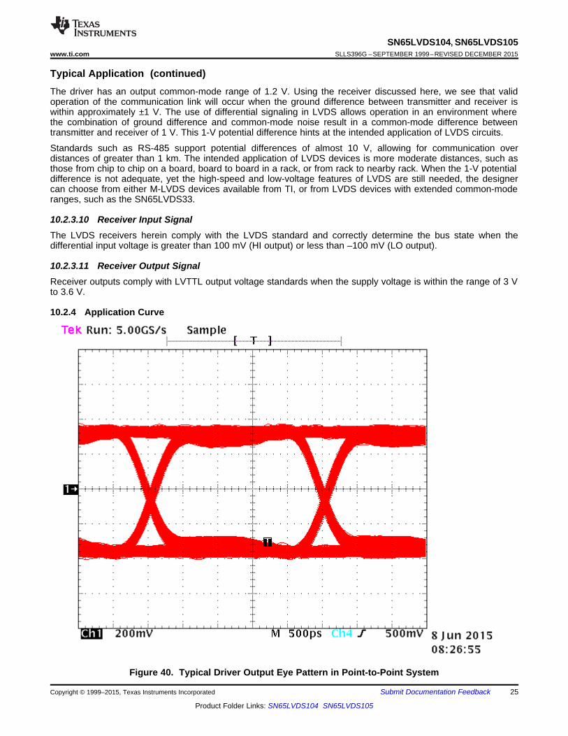
Typical Application (continued)The driver has an output common-mode range of 1.2 V. Using the receiver discussed here, we see that validoperation of the communication link will occur when the ground difference between transmitter and receiver iswithin approximately ±1 V. The use of differential signaling in LVDS allows operation in an environment wherethe combination of ground difference and common-mode noise result in a common-mode difference betweentransmitter and receiver of 1 V. This 1-V potential difference hints at the intended application of LVDS circuits.
Standards such as RS-485 support potential differences of almost 10 V, allowing for communication overdistances of greater than 1 km. The intended application of LVDS devices is more moderate distances, such asthose from chip to chip on a board, board to board in a rack, or from rack to nearby rack. When the 1-V potentialdifference is not adequate, yet the high-speed and low-voltage features of LVDS are still needed, the designercan choose from either M-LVDS devices available from TI, or from LVDS devices with extended common-moderanges, such as the SN65LVDS33.
10.2.3.10 Receiver Input SignalThe LVDS receivers herein comply with the LVDS standard and correctly determine the bus state when thedifferential input voltage is greater than 100 mV (HI output) or less than –100 mV (LO output).
10.2.3.11 Receiver Output SignalReceiver outputs comply with LVTTL output voltage standards when the supply voltage is within the range of 3 Vto 3.6 V.
10.2.4 Application Curve
Figure 40. Typical Driver Output Eye Pattern in Point-to-Point System
Copyright © 1999–2015, Texas Instruments Incorporated Submit Documentation Feedback 25
Product Folder Links: SN65LVDS104 SN65LVDS105
Driver
+
±≈100
Ω
Receiver
Minimize
Stub
Lengths
Minimize
Stub
Lengths
+±
Receiv
er +±
Receiv
er
SN65LVDS104, SN65LVDS105SLLS396G –SEPTEMBER 1999–REVISED DECEMBER 2015 www.ti.com
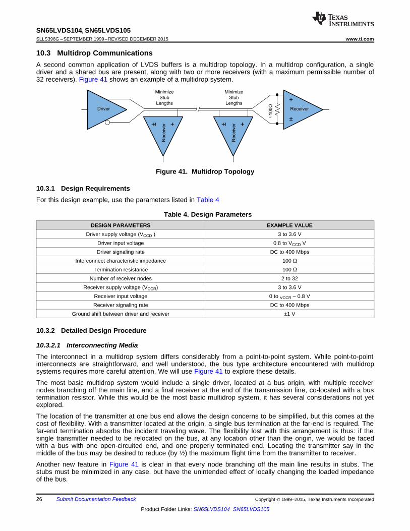
10.3 Multidrop CommunicationsA second common application of LVDS buffers is a multidrop topology. In a multidrop configuration, a singledriver and a shared bus are present, along with two or more receivers (with a maximum permissible number of32 receivers). Figure 41 shows an example of a multidrop system.
Figure 41. Multidrop Topology
10.3.1 Design RequirementsFor this design example, use the parameters listed in Table 4
Table 4. Design ParametersDESIGN PARAMETERS EXAMPLE VALUE
Driver supply voltage (VCCD ) 3 to 3.6 VDriver input voltage 0.8 to VCCD VDriver signaling rate DC to 400 Mbps
Interconnect characteristic impedance 100 ΩTermination resistance 100 Ω
Number of receiver nodes 2 to 32Receiver supply voltage (VCCR) 3 to 3.6 V
Receiver input voltage 0 to VCCR – 0.8 VReceiver signaling rate DC to 400 Mbps
Ground shift between driver and receiver ±1 V
10.3.2 Detailed Design Procedure
10.3.2.1 Interconnecting MediaThe interconnect in a multidrop system differs considerably from a point-to-point system. While point-to-pointinterconnects are straightforward, and well understood, the bus type architecture encountered with multidropsystems requires more careful attention. We will use Figure 41 to explore these details.
The most basic multidrop system would include a single driver, located at a bus origin, with multiple receivernodes branching off the main line, and a final receiver at the end of the transmission line, co-located with a bustermination resistor. While this would be the most basic multidrop system, it has several considerations not yetexplored.
The location of the transmitter at one bus end allows the design concerns to be simplified, but this comes at thecost of flexibility. With a transmitter located at the origin, a single bus termination at the far-end is required. Thefar-end termination absorbs the incident traveling wave. The flexibility lost with this arrangement is thus: if thesingle transmitter needed to be relocated on the bus, at any location other than the origin, we would be facedwith a bus with one open-circuited end, and one properly terminated end. Locating the transmitter say in themiddle of the bus may be desired to reduce (by ½) the maximum flight time from the transmitter to receiver.
Another new feature in Figure 41 is clear in that every node branching off the main line results in stubs. Thestubs must be minimized in any case, but have the unintended effect of locally changing the loaded impedanceof the bus.
26 Submit Documentation Feedback Copyright © 1999–2015, Texas Instruments Incorporated
Product Folder Links: SN65LVDS104 SN65LVDS105
SN65LVDS104, SN65LVDS105www.ti.com SLLS396G –SEPTEMBER 1999–REVISED DECEMBER 2015
To a good approximation, the characteristic transmission line impedance of an unloaded multipoint or multidropbus is defined by √L/C, where L is the inductance per unit length and C is the capacitance per unit length. Ascapacitance is added to the bus in the form of devices and interconnections, the bus characteristic impedance islowered. This may result in signal reflections from the impedance mismatch between the unloaded and loadedsegments of the bus.
If the number of loads is constant and can be distributed evenly along the line, reflections can be reduced bychanging the bus termination resistors to match the loaded characteristic impedance. Normally, the number ofloads are not constant or distributed evenly and the reflections resulting from any mismatching must beaccounted for in the noise budget.
11 Power Supply Recommendations
11.1 Coupling Capacitor RecommendationsTo minimize the power supply noise floor, provide good decoupling near the SN65LVDS10x power pins. It isrecommended to place one 0.01-μF ceramic capacitor at each power pin, and two 0.1-μF ceramic capacitors oneach power node. The distance between the device and capacitors must be minimized to reduce loop inductanceand provide optimal noise filtering. Placing the capacitor underneath the device on the bottom of the PCB is oftena good choice. A 100-pF ceramic capacitor can be put at each power pin to optimize the EMI performance.
12 Layout
12.1 Layout Guidelines
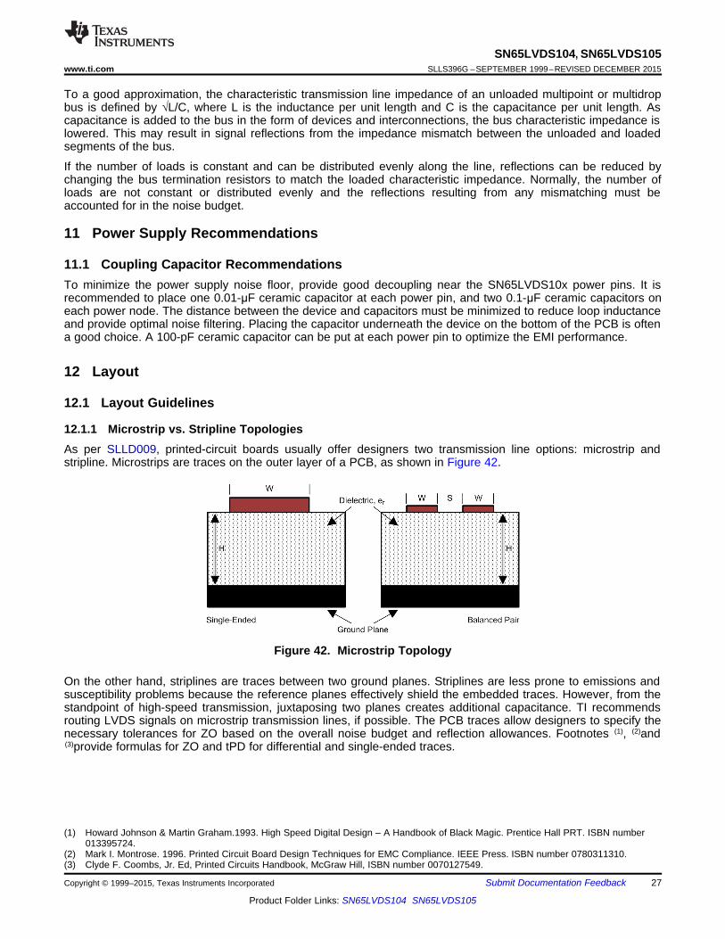
12.1.1 Microstrip vs. Stripline TopologiesAs per SLLD009, printed-circuit boards usually offer designers two transmission line options: microstrip andstripline. Microstrips are traces on the outer layer of a PCB, as shown in Figure 42.
Figure 42. Microstrip Topology
On the other hand, striplines are traces between two ground planes. Striplines are less prone to emissions andsusceptibility problems because the reference planes effectively shield the embedded traces. However, from thestandpoint of high-speed transmission, juxtaposing two planes creates additional capacitance. TI recommendsrouting LVDS signals on microstrip transmission lines, if possible. The PCB traces allow designers to specify thenecessary tolerances for ZO based on the overall noise budget and reflection allowances. Footnotes (1), (2)and(3)provide formulas for ZO and tPD for differential and single-ended traces.
(1) Howard Johnson & Martin Graham.1993. High Speed Digital Design – A Handbook of Black Magic. Prentice Hall PRT. ISBN number013395724.
(2) Mark I. Montrose. 1996. Printed Circuit Board Design Techniques for EMC Compliance. IEEE Press. ISBN number 0780311310.(3) Clyde F. Coombs, Jr. Ed, Printed Circuits Handbook, McGraw Hill, ISBN number 0070127549.
Copyright © 1999–2015, Texas Instruments Incorporated Submit Documentation Feedback 27
Product Folder Links: SN65LVDS104 SN65LVDS105
Layer 4: Routed Plane (TTL/CMOS Signals)
Layer 3: Power Plane
Layer 2: Ground Plane
Layer 1: Routed Plane (LVDS Signals)
SN65LVDS104, SN65LVDS105SLLS396G –SEPTEMBER 1999–REVISED DECEMBER 2015 www.ti.com
Layout Guidelines (continued)
Figure 43. Stripline Topology
12.1.2 Dielectric Type and Board ConstructionThe speeds at which signals travel across the board dictates the choice of dielectric. FR-4, or equivalent, usuallyprovides adequate performance for use with LVDS signals. If rise or fall times of TTL/CMOS signals are lessthan 500 ps, empirical results indicate that a material with a dielectric constant near 3.4, such as Rogers™ 4350or Nelco N4000-13 is better suited. Once the designer chooses the dielectric, there are several parameterspertaining to the board construction that can affect performance. The following set of guidelines were developedexperimentally through several designs involving LVDS devices:
• Copper weight: 15 g or 1/2 oz start, plated to 30 g or 1 oz• All exposed circuitry must be solder-plated (60/40) to 7.62 μm or 0.0003 in. (minimum)• Copper must must be 25.4 μm or 0.001 in. (minimum)
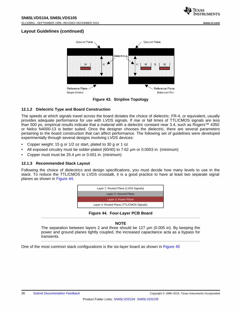
12.1.3 Recommended Stack LayoutFollowing the choice of dielectrics and design specifications, you must decide how many levels to use in thestack. To reduce the TTL/CMOS to LVDS crosstalk, it is a good practice to have at least two separate signalplanes as shown in Figure 44.
Figure 44. Four-Layer PCB Board
NOTEThe separation between layers 2 and three should be 127 µm (0.005 in). By keeping thepower and ground planes tightly coupled, the increased capacitance acta as a bypass fortransients.
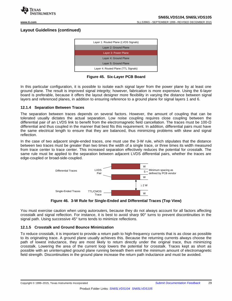
One of the most common stack configurations is the six-layer board as shown in Figure 45
28 Submit Documentation Feedback Copyright © 1999–2015, Texas Instruments Incorporated
Product Folder Links: SN65LVDS104 SN65LVDS105
t2 W
W
W
W
Minimum spacing asdefined by PCB vendor
LVDSPair
TTL/CMOSTrace
Differential Traces
Single-Ended Traces
S =
Layer 4: Routed Plane (TTL Signals)
Layer 3: Power Plane
Layer 2: Ground Plane
Layer 1: Routed Plane (LVDS Signals)
Layer 4: Ground Plane
Layer 5: Ground Plane
SN65LVDS104, SN65LVDS105www.ti.com SLLS396G –SEPTEMBER 1999–REVISED DECEMBER 2015
Layout Guidelines (continued)
Figure 45. Six-Layer PCB Board
In this particular configuration, it is possible to isolate each signal layer from the power plane by at least oneground plane. The result is improved signal integrity; however, fabrication is more expensive. Using the 6-layerboard is preferable, because it offers the layout designer more flexibility in varying the distance between signallayers and referenced planes, in addition to ensuring reference to a ground plane for signal layers 1 and 6.
12.1.4 Separation Between TracesThe separation between traces depends on several factors. However, the amount of coupling that can betolerated usually dictates the actual separation. Low noise coupling requires close coupling between thedifferential pair of an LVDS link to benefit from the electromagnetic field cancellation. The traces must be 100-Ωdifferential and thus coupled in the manner that best fits this requirement. In addition, differential pairs must havethe same electrical length to ensure that they are balanced, thus minimizing problems with skew and signalreflection.
In the case of two adjacent single-ended traces, one must use the 3-W rule, which stipulates that the distancebetween two traces must be greater than two times the width of a single trace, or three times its width measuredfrom trace center to trace center. This increased separation effectively reduces the potential for crosstalk. Thesame rule must be applied to the separation between adjacent LVDS differential pairs, whether the traces areedge-coupled or broad-side-coupled.
Figure 46. 3-W Rule for Single-Ended and Differential Traces (Top View)
You must exercise caution when using autorouters, because they do not always account for all factors affectingcrosstalk and signal reflection. For instance, it is best to avoid sharp 90° turns to prevent discontinuities in thesignal path. Using successive 45° turns tends to minimize reflections.
12.1.5 Crosstalk and Ground Bounce MinimizationTo reduce crosstalk, it is important to provide a return path to high-frequency currents that is as close as possibleto its originating trace. A ground plane usually achieves this. Because the returning currents always choose thepath of lowest inductance, they are most likely to return directly under the original trace, thus minimizingcrosstalk. Lowering the area of the current loop lowers the potential for crosstalk. Traces kept as short aspossible with an uninterrupted ground plane running beneath them emit the minimum amount of electromagneticfield strength. Discontinuities in the ground plane increase the return path inductance and must be avoided.
Copyright © 1999–2015, Texas Instruments Incorporated Submit Documentation Feedback 29
Product Folder Links: SN65LVDS104 SN65LVDS105
Boa
rd th
ickn
ess
appr
oxim
atel
y 10
0 m
il
2 mil
Typical 12-Layer PCB
4 mil
4 mil
6 mil
6 mil
VCCVia
GNDVia
TOP signal layer + GND fill
VDD 1 planeGND planeSignal layer
Buried capacitor>
Signal layerGND plane
VDD 2 planeBOTTOM signal layer + GND fill
Buried capacitor>
GND plane
Signal layers
VCC plane
SN65LVDS104, SN65LVDS105SLLS396G –SEPTEMBER 1999–REVISED DECEMBER 2015 www.ti.com
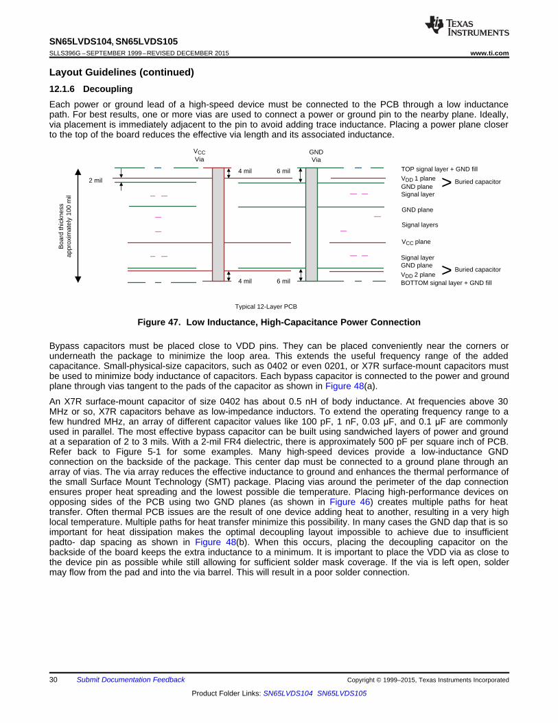
Layout Guidelines (continued)12.1.6 DecouplingEach power or ground lead of a high-speed device must be connected to the PCB through a low inductancepath. For best results, one or more vias are used to connect a power or ground pin to the nearby plane. Ideally,via placement is immediately adjacent to the pin to avoid adding trace inductance. Placing a power plane closerto the top of the board reduces the effective via length and its associated inductance.
Figure 47. Low Inductance, High-Capacitance Power Connection
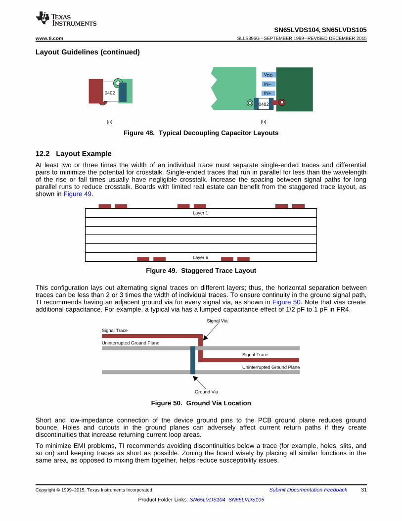
Bypass capacitors must be placed close to VDD pins. They can be placed conveniently near the corners orunderneath the package to minimize the loop area. This extends the useful frequency range of the addedcapacitance. Small-physical-size capacitors, such as 0402 or even 0201, or X7R surface-mount capacitors mustbe used to minimize body inductance of capacitors. Each bypass capacitor is connected to the power and groundplane through vias tangent to the pads of the capacitor as shown in Figure 48(a).
An X7R surface-mount capacitor of size 0402 has about 0.5 nH of body inductance. At frequencies above 30MHz or so, X7R capacitors behave as low-impedance inductors. To extend the operating frequency range to afew hundred MHz, an array of different capacitor values like 100 pF, 1 nF, 0.03 μF, and 0.1 μF are commonlyused in parallel. The most effective bypass capacitor can be built using sandwiched layers of power and groundat a separation of 2 to 3 mils. With a 2-mil FR4 dielectric, there is approximately 500 pF per square inch of PCB.Refer back to Figure 5-1 for some examples. Many high-speed devices provide a low-inductance GNDconnection on the backside of the package. This center dap must be connected to a ground plane through anarray of vias. The via array reduces the effective inductance to ground and enhances the thermal performance ofthe small Surface Mount Technology (SMT) package. Placing vias around the perimeter of the dap connectionensures proper heat spreading and the lowest possible die temperature. Placing high-performance devices onopposing sides of the PCB using two GND planes (as shown in Figure 46) creates multiple paths for heattransfer. Often thermal PCB issues are the result of one device adding heat to another, resulting in a very highlocal temperature. Multiple paths for heat transfer minimize this possibility. In many cases the GND dap that is soimportant for heat dissipation makes the optimal decoupling layout impossible to achieve due to insufficientpadto- dap spacing as shown in Figure 48(b). When this occurs, placing the decoupling capacitor on thebackside of the board keeps the extra inductance to a minimum. It is important to place the VDD via as close tothe device pin as possible while still allowing for sufficient solder mask coverage. If the via is left open, soldermay flow from the pad and into the via barrel. This will result in a poor solder connection.
30 Submit Documentation Feedback Copyright © 1999–2015, Texas Instruments Incorporated
Product Folder Links: SN65LVDS104 SN65LVDS105
Signal Trace
Uninterrupted Ground Plane
Signal Trace
Uninterrupted Ground Plane
Signal Via
Ground Via
Layer 6
Layer 1
0402
0402
VDD
IN±
IN+
(a) (b)
SN65LVDS104, SN65LVDS105www.ti.com SLLS396G –SEPTEMBER 1999–REVISED DECEMBER 2015
Layout Guidelines (continued)
Figure 48. Typical Decoupling Capacitor Layouts
12.2 Layout ExampleAt least two or three times the width of an individual trace must separate single-ended traces and differentialpairs to minimize the potential for crosstalk. Single-ended traces that run in parallel for less than the wavelengthof the rise or fall times usually have negligible crosstalk. Increase the spacing between signal paths for longparallel runs to reduce crosstalk. Boards with limited real estate can benefit from the staggered trace layout, asshown in Figure 49.
Figure 49. Staggered Trace Layout
This configuration lays out alternating signal traces on different layers; thus, the horizontal separation betweentraces can be less than 2 or 3 times the width of individual traces. To ensure continuity in the ground signal path,TI recommends having an adjacent ground via for every signal via, as shown in Figure 50. Note that vias createadditional capacitance. For example, a typical via has a lumped capacitance effect of 1/2 pF to 1 pF in FR4.
Figure 50. Ground Via Location
Short and low-impedance connection of the device ground pins to the PCB ground plane reduces groundbounce. Holes and cutouts in the ground planes can adversely affect current return paths if they creatediscontinuities that increase returning current loop areas.
To minimize EMI problems, TI recommends avoiding discontinuities below a trace (for example, holes, slits, andso on) and keeping traces as short as possible. Zoning the board wisely by placing all similar functions in thesame area, as opposed to mixing them together, helps reduce susceptibility issues.
Copyright © 1999–2015, Texas Instruments Incorporated Submit Documentation Feedback 31
Product Folder Links: SN65LVDS104 SN65LVDS105
SN65LVDS104, SN65LVDS105SLLS396G –SEPTEMBER 1999–REVISED DECEMBER 2015 www.ti.com
13 Device and Documentation Support
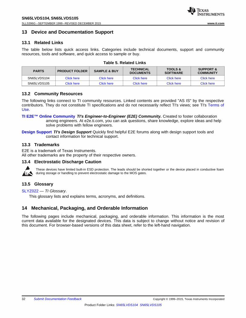
13.1 Related LinksThe table below lists quick access links. Categories include technical documents, support and communityresources, tools and software, and quick access to sample or buy.
Table 5. Related LinksTECHNICAL TOOLS & SUPPORT &PARTS PRODUCT FOLDER SAMPLE & BUY DOCUMENTS SOFTWARE COMMUNITY
SN65LVDS104 Click here Click here Click here Click here Click hereSN65LVDS105 Click here Click here Click here Click here Click here
13.2 Community ResourcesThe following links connect to TI community resources. Linked contents are provided "AS IS" by the respectivecontributors. They do not constitute TI specifications and do not necessarily reflect TI's views; see TI's Terms ofUse.
TI E2E™ Online Community TI's Engineer-to-Engineer (E2E) Community. Created to foster collaborationamong engineers. At e2e.ti.com, you can ask questions, share knowledge, explore ideas and helpsolve problems with fellow engineers.
Design Support TI's Design Support Quickly find helpful E2E forums along with design support tools andcontact information for technical support.
13.3 TrademarksE2E is a trademark of Texas Instruments.All other trademarks are the property of their respective owners.
13.4 Electrostatic Discharge CautionThese devices have limited built-in ESD protection. The leads should be shorted together or the device placed in conductive foamduring storage or handling to prevent electrostatic damage to the MOS gates.
13.5 GlossarySLYZ022 — TI Glossary.
This glossary lists and explains terms, acronyms, and definitions.
14 Mechanical, Packaging, and Orderable InformationThe following pages include mechanical, packaging, and orderable information. This information is the mostcurrent data available for the designated devices. This data is subject to change without notice and revision ofthis document. For browser-based versions of this data sheet, refer to the left-hand navigation.
32 Submit Documentation Feedback Copyright © 1999–2015, Texas Instruments Incorporated
Product Folder Links: SN65LVDS104 SN65LVDS105
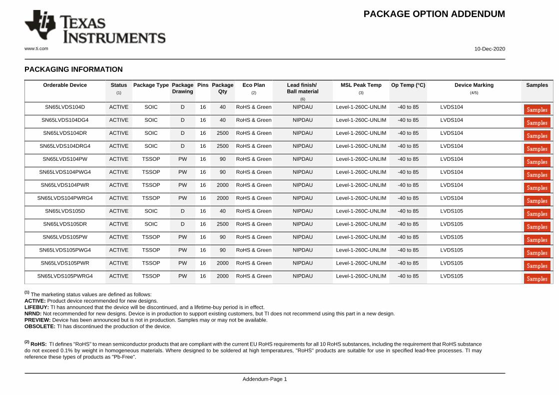
PACKAGE OPTION ADDENDUM
www.ti.com 10-Dec-2020
Addendum-Page 1
PACKAGING INFORMATION
Orderable Device Status(1)
Package Type PackageDrawing
Pins PackageQty
Eco Plan(2)
Lead finish/Ball material
(6)
MSL Peak Temp(3)
Op Temp (°C) Device Marking(4/5)
Samples
SN65LVDS104D ACTIVE SOIC D 16 40 RoHS & Green NIPDAU Level-1-260C-UNLIM -40 to 85 LVDS104
SN65LVDS104DG4 ACTIVE SOIC D 16 40 RoHS & Green NIPDAU Level-1-260C-UNLIM -40 to 85 LVDS104
SN65LVDS104DR ACTIVE SOIC D 16 2500 RoHS & Green NIPDAU Level-1-260C-UNLIM -40 to 85 LVDS104
SN65LVDS104DRG4 ACTIVE SOIC D 16 2500 RoHS & Green NIPDAU Level-1-260C-UNLIM -40 to 85 LVDS104
SN65LVDS104PW ACTIVE TSSOP PW 16 90 RoHS & Green NIPDAU Level-1-260C-UNLIM -40 to 85 LVDS104
SN65LVDS104PWG4 ACTIVE TSSOP PW 16 90 RoHS & Green NIPDAU Level-1-260C-UNLIM -40 to 85 LVDS104
SN65LVDS104PWR ACTIVE TSSOP PW 16 2000 RoHS & Green NIPDAU Level-1-260C-UNLIM -40 to 85 LVDS104
SN65LVDS104PWRG4 ACTIVE TSSOP PW 16 2000 RoHS & Green NIPDAU Level-1-260C-UNLIM -40 to 85 LVDS104
SN65LVDS105D ACTIVE SOIC D 16 40 RoHS & Green NIPDAU Level-1-260C-UNLIM -40 to 85 LVDS105
SN65LVDS105DR ACTIVE SOIC D 16 2500 RoHS & Green NIPDAU Level-1-260C-UNLIM -40 to 85 LVDS105
SN65LVDS105PW ACTIVE TSSOP PW 16 90 RoHS & Green NIPDAU Level-1-260C-UNLIM -40 to 85 LVDS105
SN65LVDS105PWG4 ACTIVE TSSOP PW 16 90 RoHS & Green NIPDAU Level-1-260C-UNLIM -40 to 85 LVDS105
SN65LVDS105PWR ACTIVE TSSOP PW 16 2000 RoHS & Green NIPDAU Level-1-260C-UNLIM -40 to 85 LVDS105
SN65LVDS105PWRG4 ACTIVE TSSOP PW 16 2000 RoHS & Green NIPDAU Level-1-260C-UNLIM -40 to 85 LVDS105
(1) The marketing status values are defined as follows:ACTIVE: Product device recommended for new designs.LIFEBUY: TI has announced that the device will be discontinued, and a lifetime-buy period is in effect.NRND: Not recommended for new designs. Device is in production to support existing customers, but TI does not recommend using this part in a new design.PREVIEW: Device has been announced but is not in production. Samples may or may not be available.OBSOLETE: TI has discontinued the production of the device.
(2) RoHS: TI defines "RoHS" to mean semiconductor products that are compliant with the current EU RoHS requirements for all 10 RoHS substances, including the requirement that RoHS substancedo not exceed 0.1% by weight in homogeneous materials. Where designed to be soldered at high temperatures, "RoHS" products are suitable for use in specified lead-free processes. TI mayreference these types of products as "Pb-Free".
PACKAGE OPTION ADDENDUM
www.ti.com 10-Dec-2020
Addendum-Page 2
RoHS Exempt: TI defines "RoHS Exempt" to mean products that contain lead but are compliant with EU RoHS pursuant to a specific EU RoHS exemption.Green: TI defines "Green" to mean the content of Chlorine (Cl) and Bromine (Br) based flame retardants meet JS709B low halogen requirements of <=1000ppm threshold. Antimony trioxide basedflame retardants must also meet the <=1000ppm threshold requirement.
(3) MSL, Peak Temp. - The Moisture Sensitivity Level rating according to the JEDEC industry standard classifications, and peak solder temperature.
(4) There may be additional marking, which relates to the logo, the lot trace code information, or the environmental category on the device.
(5) Multiple Device Markings will be inside parentheses. Only one Device Marking contained in parentheses and separated by a "~" will appear on a device. If a line is indented then it is a continuationof the previous line and the two combined represent the entire Device Marking for that device.
(6) Lead finish/Ball material - Orderable Devices may have multiple material finish options. Finish options are separated by a vertical ruled line. Lead finish/Ball material values may wrap to twolines if the finish value exceeds the maximum column width.
Important Information and Disclaimer:The information provided on this page represents TI's knowledge and belief as of the date that it is provided. TI bases its knowledge and belief on informationprovided by third parties, and makes no representation or warranty as to the accuracy of such information. Efforts are underway to better integrate information from third parties. TI has taken andcontinues to take reasonable steps to provide representative and accurate information but may not have conducted destructive testing or chemical analysis on incoming materials and chemicals.TI and TI suppliers consider certain information to be proprietary, and thus CAS numbers and other limited information may not be available for release.
In no event shall TI's liability arising out of such information exceed the total purchase price of the TI part(s) at issue in this document sold by TI to Customer on an annual basis.
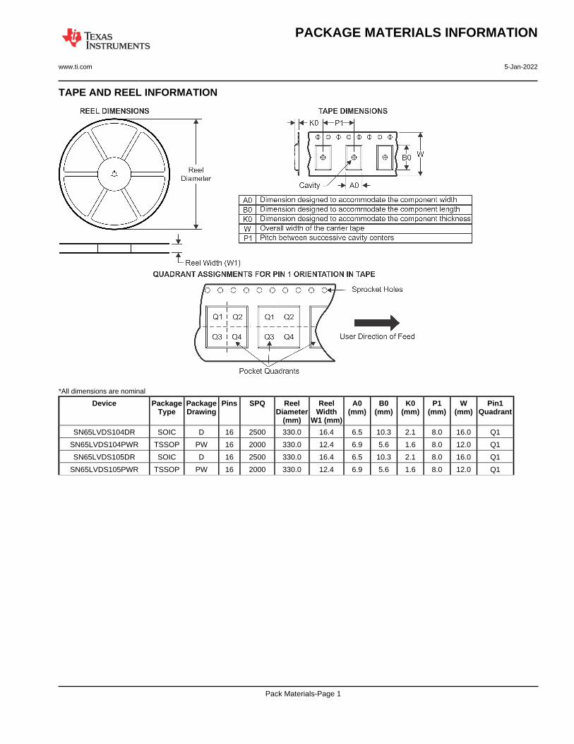
TAPE AND REEL INFORMATION
*All dimensions are nominal
Device PackageType
PackageDrawing
Pins SPQ ReelDiameter
(mm)
ReelWidth
W1 (mm)
A0(mm)
B0(mm)
K0(mm)
P1(mm)
W(mm)
Pin1Quadrant
SN65LVDS104DR SOIC D 16 2500 330.0 16.4 6.5 10.3 2.1 8.0 16.0 Q1
SN65LVDS104PWR TSSOP PW 16 2000 330.0 12.4 6.9 5.6 1.6 8.0 12.0 Q1
SN65LVDS105DR SOIC D 16 2500 330.0 16.4 6.5 10.3 2.1 8.0 16.0 Q1
SN65LVDS105PWR TSSOP PW 16 2000 330.0 12.4 6.9 5.6 1.6 8.0 12.0 Q1
PACKAGE MATERIALS INFORMATION
www.ti.com 5-Jan-2022
Pack Materials-Page 1
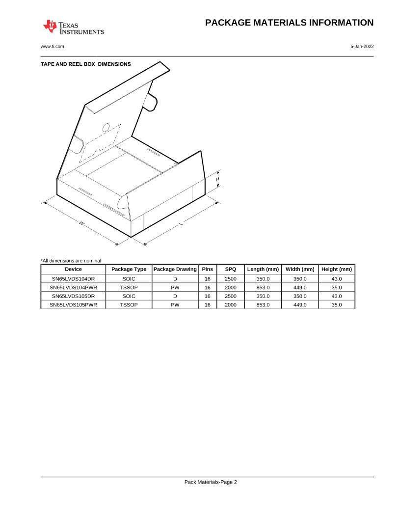
*All dimensions are nominal
Device Package Type Package Drawing Pins SPQ Length (mm) Width (mm) Height (mm)
SN65LVDS104DR SOIC D 16 2500 350.0 350.0 43.0
SN65LVDS104PWR TSSOP PW 16 2000 853.0 449.0 35.0
SN65LVDS105DR SOIC D 16 2500 350.0 350.0 43.0
SN65LVDS105PWR TSSOP PW 16 2000 853.0 449.0 35.0
PACKAGE MATERIALS INFORMATION
www.ti.com 5-Jan-2022
Pack Materials-Page 2
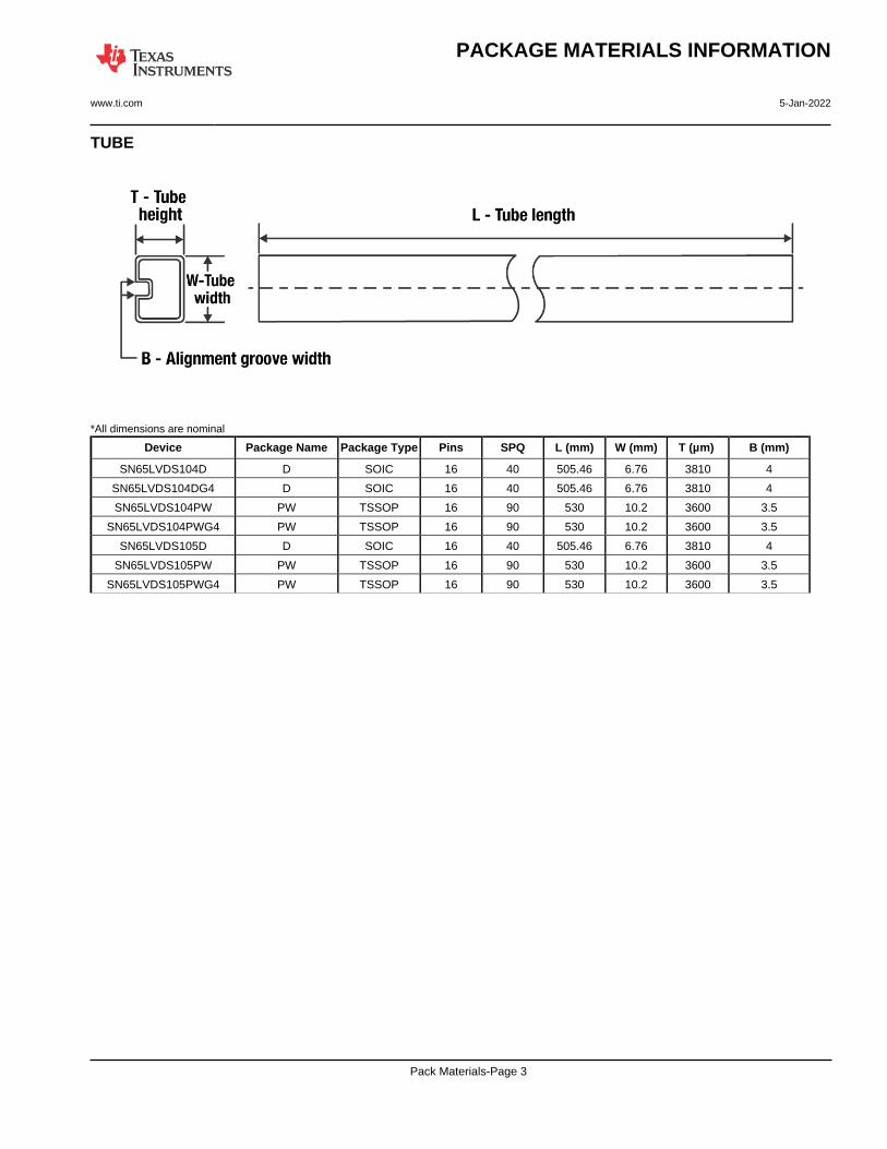
TUBE
*All dimensions are nominal
Device Package Name Package Type Pins SPQ L (mm) W (mm) T (µm) B (mm)
SN65LVDS104D D SOIC 16 40 505.46 6.76 3810 4
SN65LVDS104DG4 D SOIC 16 40 505.46 6.76 3810 4
SN65LVDS104PW PW TSSOP 16 90 530 10.2 3600 3.5
SN65LVDS104PWG4 PW TSSOP 16 90 530 10.2 3600 3.5
SN65LVDS105D D SOIC 16 40 505.46 6.76 3810 4
SN65LVDS105PW PW TSSOP 16 90 530 10.2 3600 3.5
SN65LVDS105PWG4 PW TSSOP 16 90 530 10.2 3600 3.5
PACKAGE MATERIALS INFORMATION
www.ti.com 5-Jan-2022
Pack Materials-Page 3
www.ti.com
PACKAGE OUTLINE
C
14X 0.65
2X4.55
16X 0.300.19
TYP6.66.2
1.2 MAX
0.150.05
0.25GAGE PLANE
-80
BNOTE 4
4.54.3
A
NOTE 3
5.14.9
0.750.50
(0.15) TYP
TSSOP - 1.2 mm max heightPW0016ASMALL OUTLINE PACKAGE
4220204/A 02/2017
1
89
16
0.1 C A B
PIN 1 INDEX AREA
SEE DETAIL A
0.1 C
NOTES: 1. All linear dimensions are in millimeters. Any dimensions in parenthesis are for reference only. Dimensioning and tolerancing per ASME Y14.5M. 2. This drawing is subject to change without notice. 3. This dimension does not include mold flash, protrusions, or gate burrs. Mold flash, protrusions, or gate burrs shall not exceed 0.15 mm per side. 4. This dimension does not include interlead flash. Interlead flash shall not exceed 0.25 mm per side.5. Reference JEDEC registration MO-153.
SEATINGPLANE
A 20DETAIL ATYPICAL
SCALE 2.500
www.ti.com
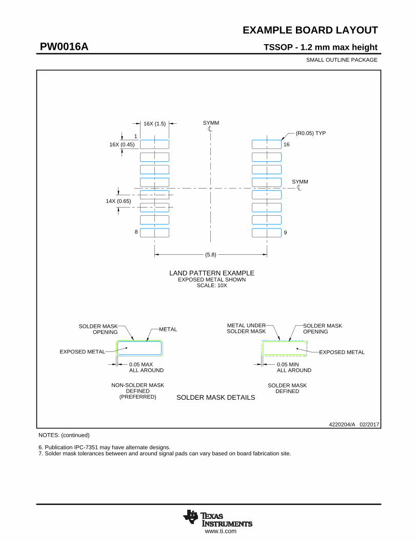
EXAMPLE BOARD LAYOUT
0.05 MAXALL AROUND
0.05 MINALL AROUND
16X (1.5)
16X (0.45)
14X (0.65)
(5.8)
(R0.05) TYP
TSSOP - 1.2 mm max heightPW0016ASMALL OUTLINE PACKAGE
4220204/A 02/2017
NOTES: (continued) 6. Publication IPC-7351 may have alternate designs. 7. Solder mask tolerances between and around signal pads can vary based on board fabrication site.
LAND PATTERN EXAMPLEEXPOSED METAL SHOWN
SCALE: 10X
SYMM
SYMM
1
8 9
16
15.000
METALSOLDER MASKOPENING
METAL UNDERSOLDER MASK
SOLDER MASKOPENING
EXPOSED METALEXPOSED METAL
SOLDER MASK DETAILS
NON-SOLDER MASKDEFINED
(PREFERRED)
SOLDER MASKDEFINED
www.ti.com
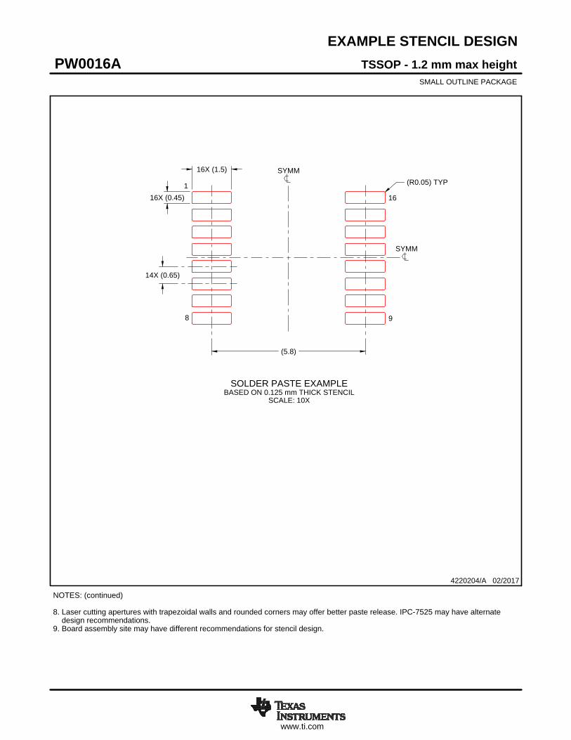
EXAMPLE STENCIL DESIGN
16X (1.5)
16X (0.45)
14X (0.65)
(5.8)
(R0.05) TYP
TSSOP - 1.2 mm max heightPW0016ASMALL OUTLINE PACKAGE
4220204/A 02/2017
NOTES: (continued) 8. Laser cutting apertures with trapezoidal walls and rounded corners may offer better paste release. IPC-7525 may have alternate design recommendations. 9. Board assembly site may have different recommendations for stencil design.
SOLDER PASTE EXAMPLEBASED ON 0.125 mm THICK STENCIL
SCALE: 10X
SYMM
SYMM
1
8 9
16

IMPORTANT NOTICE AND DISCLAIMERTI PROVIDES TECHNICAL AND RELIABILITY DATA (INCLUDING DATA SHEETS), DESIGN RESOURCES (INCLUDING REFERENCE DESIGNS), APPLICATION OR OTHER DESIGN ADVICE, WEB TOOLS, SAFETY INFORMATION, AND OTHER RESOURCES “AS IS” AND WITH ALL FAULTS, AND DISCLAIMS ALL WARRANTIES, EXPRESS AND IMPLIED, INCLUDING WITHOUT LIMITATION ANY IMPLIED WARRANTIES OF MERCHANTABILITY, FITNESS FOR A PARTICULAR PURPOSE OR NON-INFRINGEMENT OF THIRD PARTY INTELLECTUAL PROPERTY RIGHTS.These resources are intended for skilled developers designing with TI products. You are solely responsible for (1) selecting the appropriate TI products for your application, (2) designing, validating and testing your application, and (3) ensuring your application meets applicable standards, and any other safety, security, regulatory or other requirements.These resources are subject to change without notice. TI grants you permission to use these resources only for development of an application that uses the TI products described in the resource. Other reproduction and display of these resources is prohibited. No license is granted to any other TI intellectual property right or to any third party intellectual property right. TI disclaims responsibility for, and you will fully indemnify TI and its representatives against, any claims, damages, costs, losses, and liabilities arising out of your use of these resources.TI’s products are provided subject to TI’s Terms of Sale or other applicable terms available either on ti.com or provided in conjunction with such TI products. TI’s provision of these resources does not expand or otherwise alter TI’s applicable warranties or warranty disclaimers for TI products.TI objects to and rejects any additional or different terms you may have proposed. IMPORTANT NOTICE
Mailing Address: Texas Instruments, Post Office Box 655303, Dallas, Texas 75265Copyright © 2022, Texas Instruments Incorporated