synthesis and scripting techniques for designing multi- asynchronous clock · pdf...
TRANSCRIPT

Synthesis and Scripting Techniques for Designing Multi-Asynchronous Clock Designs
Clifford E. Cummings
Sunburst Design, Inc.
ABSTRACT
Designing a pure, one-clock synchronous design is a luxury that few ASIC designers will everknow. Most of the ASICs that are ever designed are driven by multiple asynchronous clocks andrequire special data, control-signal and verification handling to insure the timely completion of arobust working design.
SNUG-2001San Jose, CA
Voted Best Paper3rd Place
SNUG San Jose 2001 Synthesis and Scripting Techniques forRev 1.1 Designing Multi-Asynchronous Clock Designs
2
1.0 Introduction
Most college courses teach engineering students prescribed techniques for designing completelysynchronous (single clock) logic. In the real ASIC design world, there are very few single clockdesigns. This paper will detail some of the hardware design, timing analysis, synthesis andsimulation methodologies to address multi-clock designs.
This paper is not intended to provide exhaustive coverage of this topic, but is presented to sharetechniques learned from experience.
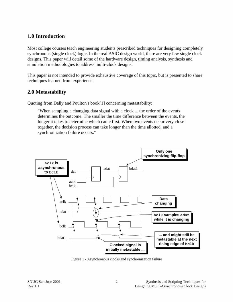
2.0 Metastability
Quoting from Dally and Poulton's book[1] concerning metastability:
"When sampling a changing data signal with a clock ... the order of the eventsdetermines the outcome. The smaller the time difference between the events, thelonger it takes to determine which came first. When two events occur very closetogether, the decision process can take longer than the time allotted, and asynchronization failure occurs."
Datachanging
bclk samples adatwhile it is changing
aclkbclk
datadat bdat1
adat
bdat1
aclk
bclk
Clocked signal isinitially metastable ...
... and might still bemetastable at the next
rising edge of bclk
aclk isasynchronous
to bclk
Only onesynchronizing flip-flop
Figure 1 - Asynchronous clocks and synchronization failure

SNUG San Jose 2001 Synthesis and Scripting Techniques forRev 1.1 Designing Multi-Asynchronous Clock Designs
3
Figure 1 shows a synchronization failure that occurs when a signal generated in one clockdomain is sampled too close to the rising edge of a clock signal from another clock domain.
Synchronization failure is caused by an output going metastable and not converging to a legalstable state by the time the output must be sampled again. Figure 2 shows that a metastableoutput can cause illegal signal values to be propagated throughout the rest of the design.
aclkbclk
datadat bdat1
adat
bdat1
aclk
bclk
"1"
"0"
????
??
??
adatchanging
Samplingclock
Clocked signal isinitially metastableand is still meta-
stable on the nextactive clock edge
Other logic output valuesare indeterminate
invalid data propagatedthroughout the design
Figure 2 - Metastable bdat1 output propagating invalid data throughout the design
Every flip-flop that is used in any design has a specified setup and hold time, or the time in whichthe data input is not legally permitted to change before and after a rising clock edge. This timewindow is specified as a design parameter precisely to keep a data signal from changing too closeto another synchronizing signal that could cause the output to go metastable.
The metastable output problem shown in Figure 2 is sometimes known as the John CooleyESNUG effect, or in other words, the propagation of unwanted information!(Just kidding, John! ☺)

SNUG San Jose 2001 Synthesis and Scripting Techniques forRev 1.1 Designing Multi-Asynchronous Clock Designs
4
3.0 Synchronizers
Quoting again from Dally and Poulton[2] concerning synchronizers:
"A synchronizer is a device that samples an asynchronous signal and outputs a versionof the signal that has transitions synchronized to a local or sample clock."
The most common synchronizer used by digital designers is a two-flip-flop synchronizer asshown in Figure 3.
aclkbclk
datadat bdat1 bdat2
adat
bdat1
bdat2
aclk
bclk
"0"
"0"
"0""1"
"1"
"1"
adatchanging
Samplingclock
Clocked signal isinitially metastable
but goes "high"before the next
active clock edge
bdat2 is synchronizedand valid
Figure 3 - Two flip-flop synchronizer
The first flip-flop samples the asynchronous input signal into the new clock domain and waits fora full clock cycle to permit any metastability on the stage-1 output signal to decay, then the stage-1 signal is sampled by the same clock into a second stage flip-flop, with the intended goal thatthe stage-2 signal is now a stable and valid signal synchronized into the new clock domain.
It is theoretically possible for the stage-1 signal to still be sufficiently metastable by the time thesignal is clocked into the second stage to cause the stage-2 signal to also go metastable. Thecalculation of the probability of the time between synchronization failures (MTBF) is a functionof multiple variables including the clock frequencies used to generate the input signal and toclock the synchronizing flip-flops. One description of the MTBF calculation can be found inDally and Poulton[3].
For most synchronization applications, the two flip-flop synchronizer is sufficient to remove alllikely metastability.

SNUG San Jose 2001 Synthesis and Scripting Techniques forRev 1.1 Designing Multi-Asynchronous Clock Designs
5
4.0 Static Timing Analysis
Performing static timing analysis is the process of verifying that every signal path in a designmeets required clock-cycle timing, whether or not all of the signal paths are even possible. Statictiming analysis is not used to verify the functionality of the design, only that the design meetstiming goals. In theory, timing verification could be accomplished by running exhaustive gate-level simulations with SDF backannotation of actual timing values after a design is placed androuted. This is often referred to as dynamic timing verification.
Static timing analysis has three principal advantages over dynamic timing verification: (1) statictiming analysis tools verify every single path between any two sequential elements, (2) statictiming analysis does not require the generation of any test vectors, and (3) static timing analysistools are orders of magnitude faster than trying to do timing verification running exhaustive gate-level simulations[4].
Timing analysis using Synopsys tools on a completely synchronous design is relatively easy toperform using either DesignTime within the Synopsys Design Compiler or Design Analyzerenvironments, or by using PrimeTime.
Timing analysis on modules with two or more asynchronous clocks is error prone, more difficultand can be time consuming. Static timing analysis on signals generated from one clock domainand latched into sequential elements within a second, asynchronous clock domain is inaccurateand for the most part worthless. The timing information for a signal latched by a clock that isasynchronous to the latched signal is inaccurate because the phase relationship between thesignal and the asynchronous clock is always changing; therefore, the static timing analysis toolwould have to check an infinite number of phase relationships between the signal andasynchronous clock. The fact is, one must assume that signals that pass from one clock domain toanother at some point will violate either setup or hold times on the destination sequentialelement.
There is no good reason to perform timing analysis on signals that are generated in one clockdomain and registered in another asynchronous clock domain. It is a given that these signals DOviolate setup and hold times on the destination register. This is why synchronizers (see section3.0) are needed, to alleviate the problems that can occur when a signal is passed from one clockdomain to another.
For RTL modules that have two or more asynchronous clocks as inputs, a designer will berequired to indicate to the static timing analysis tool which signal paths should be ignored. Thisis accomplished by "setting false paths" on signals that cross from one clock domain to another.This can be a tedious and error prone job unless the guidelines in the next two sections arefollowed.
SNUG San Jose 2001 Synthesis and Scripting Techniques forRev 1.1 Designing Multi-Asynchronous Clock Designs
6
5.0 Clock Naming Conventions
Guideline: Use a clock naming convention to identify the clock source of every signal in adesign.Reason: A naming convention helps all team members to identify the clock domain for everysignal in a design and also makes grouping of signals for timing analysis easier to do usingregular expression "wild-carding" from within a synthesis script.
A number of useful clock naming conventions have been used by various design teams. One thatwas used by design engineers in 1995 while designing video ASICs for In Focus projectorsrequired that a leading prefix character be used to identify the various asynchronous clockdomains. Examples included: uClk for the microprocessor clock, vClk for the video clock anddClk for the display clock.
Each signal was synchronized to one of the clock domains in the design and each signal-namehad to include a prefix character identifying the clock domain for that signal. Any signal that wasclocked by the uClk would have a u-prefix in the signal name, such as uaddr, udata, uwrite, etc.Any signal that was clocked by the vClk would similarly have a v-prefix in the signal name, suchas vdata, vhsync, vframe, etc. The same signal naming convention was used for all signalsgenerated by any of the other clocks in the design.
Using this technique, any engineer on the ASIC design team could easily identify the clock-domain source of any signal in the design and either use the signals directly or pass the signalsthrough a synchronizer so that they could be used within a new clock domain.
The naming convention alone contributed significantly to the productivity of the design team.How do we know there was a productivity gain? One of the design engineers started his part ofthe ASIC design using his own naming convention, ignoring the convention in use by the otherdesign team members. After much confusion about the signals entering and leaving his designpartition, a team meeting was called and the non-compliant designer was "strongly encouraged"to rename the signals in his part of the design to conform to the team naming convention. Afterthe signal names were changed, it became easier to interface to the partition in question. Fewerquestions and less confusions occurred after the change.
6.0 Design Partitioning
Guideline: Only allow one clock per module.Reason: Static timing analysis and creating synthesis scripts is more easily accomplished onsingle-clock modules or groups of single-clock modules.
Guideline: Create a synchronizer module for each set of signals that pass from just one clockdomain into another clock domain.Reason: It is given that any signal passing from one clock domain to another clock domain isgoing to have setup and hold time problems. No worst-case (max time) timing analysis isrequired for synchronizer modules. Only best case (min time) timing analysis is required between

SNUG San Jose 2001 Synthesis and Scripting Techniques forRev 1.1 Designing Multi-Asynchronous Clock Designs
7
first and second stage flip-flops to ensure that all hold times are met. Also, gate-level simulationscan more easily be configured to ignore setup and hold time violations on the first stage of eachsynchronizer.
aSig3
bSig2
cSig0
cSig1
cSig2
cSig3
cClk Logicsync_a2c
sync_b2c
aSig0
bSig1
cSig1
aSig1
aSig2
aSig3
aClk Logic
sync_b2a
sync_c2a
aSig1
bSig0
cSig2
bSig1
bSig2
bSig3
bClk Logicsync_a2b
sync_c2b
aSig2
cSig3
bSig0
cSig0
Each non-synchronizer
module is nowcompletely
synchronous tojust one clock
Simple toperform statictiming analysisfor each clock
Figure 4 - Design partitioned on clock boundaries
In 1995, while working on a multi-asynchronous-clock ASIC design to be used in In Focusprojectors, I received an e-mail message from Steve Golson in which he gave me the strongrecommendation to only allow one clock per module for each module in the ASIC design[5]. Atthat time we were permitting multiple clocks per module and trying to handle timing analysis byincluding a large number of set_false_path commands in our synthesis scripts to eliminate invalidtiming-error messages.
After giving consideration to Steve's recommendation, I decided to completely re-partition theASIC design I was working on and to adhere to the recommendation to only permit one clock permodule. I took a two-week hit to my schedule to re-partition the entire ASIC. After repartitioningthe design, many of the timing analysis and synthesis tasks became trivial.
By partitioning a design to permit only one clock per module, static timing analysis becomes asignificantly easier task.
The next logical step was to partition the design so that every input module signal was alreadysynchronized to the same clock domain before entering the module. Why is this significant? If allsignals entering and leaving the module are synchronous to the clock used in the module, thedesign is now completely synchronous! Now the entire module can be static timing analyzed

SNUG San Jose 2001 Synthesis and Scripting Techniques forRev 1.1 Designing Multi-Asynchronous Clock Designs
8
without any "false paths" and Design Compiler can be used to "group" all of the same-clocksynchronous modules to perform complete, sequential static timing analysis within each clockdomain.
There is one exception to the above recommendation. Multi-clock designs require at least someRTL modules to pass signals from one clock domain to modules that are clocked within adifferent clock domain. For the In Focus ASIC designs, we created separate synchronizermodules that permitted signals from one and only one clock domain to be passed into a modulethat synchronized the signals into a new clock domain.
Using the naming convention described in section 5.0, all processor-clock generated signals (u-signals) would be used as inputs to a module that might be clocked by the video clock. Thismodule was called the "sync_u2v" module and the RTL code did nothing more than take each u-signal input and run it through a pair of flip-flops clocked by vClk. Aside from the vClk andreset inputs, every other input signal to the "sync_u2v" module had a "u" prefix and every outputsignal from that same module had a "v" prefix.
No worst-case timing analysis is required on the "sync" modules because we know that everyinput signal to these modules will have timing problems; otherwise, we would not have to passthe signals through synchronizers. The only timing analysis that we need to perform withinsynchronizer modules is min-time (hold time) analysis between the first and second flip-flopstages for each signal.
In general, if there are n asynchronous clock domains, the design will require n(n-1)synchronizer modules, two for each pair of clock signals (example: using the uClk and vClksignals: the two synchronizer modules required would be sync_u2v and sync_v2u). Only if thereare no signals that pass between two specific clock domains will a pair of synchronizer modulesnot be required.
By the way, what happened to that repartitioned In Focus ASIC design? After modifying all ofthe RTL files to create either completely synchronous modules or synchronizer modules, the taskof generating synthesis scripts became trivial. All of the script files which previously included"set_false_path" commands were either deleted or significantly simplified. All timing problemswere easily identified and fixed (because they were all within single-clock domain groupings)and the final synthesis runs completed two weeks earlier than anticipated, putting the projectback on schedule and completely justifying the decision to repartition the design.
7.0 Synthesis Scripts & Timing Analysis
Following the guidelines of section 6.0, to only permit one clock per module, to require that allsignals entering non-synchronizer modules are also in the same clock domain that is used toclock that module and to require that synchronizer modules only permit input signals from oneother clock domain, helps to simplify the timing analysis and synthesis scripting tasks associatedwith a multi-clock design.

SNUG San Jose 2001 Synthesis and Scripting Techniques forRev 1.1 Designing Multi-Asynchronous Clock Designs
9
Synthesis script commands used to address multiple clock domain issues now become a matter ofgrouping, identifying false paths and performing min-max timing analysis.
7.1 Grouping
Group together all non-synchronizer modules that are clocked within each clock domain. Onegroup should be formed for each clock domain in the design. These groups will be timingverified as if each were a separate, completely synchronous design.
7.2 Identifying False Paths
In general, only the inputs to the synchronizer modules require "set_false_path" commands. If aclock-prefix naming scheme is used (see section 5.0), then wild-cards can be used to easilyidentify all asynchronous inputs. For example, the sync_u2v module should have inputs that allstart with the letter "u". The following dc_shell command should be sufficient to eliminate allasynchronous inputs from timing analysis:
set_false_path -from { u* }
7.3 Performing Min-Max Timing Analysis
Each grouped set of modules for each clock domain is now a completely synchronous sub-designand tools such as DesignTime or PrimeTime can be used to verify worst case timing (includingsetup time checks) and best case timing (including hold time checks).
The synchronizer blocks are timing verified separately. Worst case timing checks are notrequired because these modules are just composed of flip-flops to synchronize asynchronousinput signals; therefore, there are no long path delays and the outputs are fully registered. Aftersetting false paths on all of the asynchronous inputs, best case (minimum) timing verification isconducted to insure that hold times are met on all signals that are passed from the first to secondstage synchronizing flip-flops.
8.0 Synchronizing Fast Signals Into Slow Clock Domains
A general problem associated with synchronizers is the problem that a signal from a sendingclock domain might change values twice before it can be sampled into a slower clock domain.This problem must be considered any time signals are sent from one clock domain to another.
Synchronizing slower control signals into a faster clock domain is generally not a problem sincethe faster clock signal will sample the slower control signal one or more times. Recognizing thatsampling slower signals into faster clock domains causes fewer potential problems than samplingfaster signals into slower clock domains, a designer might want to take advantage of this fact andtry to steer control signals towards faster clock domains.
SNUG San Jose 2001 Synthesis and Scripting Techniques forRev 1.1 Designing Multi-Asynchronous Clock Designs
10
8.1 Passing A Slow Control Signal
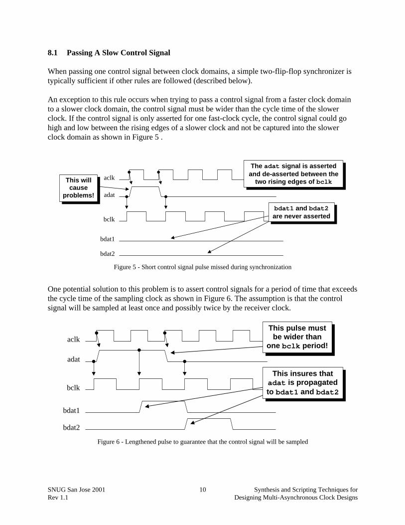
When passing one control signal between clock domains, a simple two-flip-flop synchronizer istypically sufficient if other rules are followed (described below).
An exception to this rule occurs when trying to pass a control signal from a faster clock domainto a slower clock domain, the control signal must be wider than the cycle time of the slowerclock. If the control signal is only asserted for one fast-clock cycle, the control signal could gohigh and low between the rising edges of a slower clock and not be captured into the slowerclock domain as shown in Figure 5 .
adat
bdat1
bdat2
aclk
bclk
This willcause
problems!
The adat signal is assertedand de-asserted between the
two rising edges of bclk
bdat1 and bdat2are never asserted
Figure 5 - Short control signal pulse missed during synchronization
One potential solution to this problem is to assert control signals for a period of time that exceedsthe cycle time of the sampling clock as shown in Figure 6. The assumption is that the controlsignal will be sampled at least once and possibly twice by the receiver clock.
adat
bdat1
bdat2
aclk
bclk
This pulse mustbe wider than
one bclk period!
This insures thatadat is propagatedto bdat1 and bdat2
Figure 6 - Lengthened pulse to guarantee that the control signal will be sampled
SNUG San Jose 2001 Synthesis and Scripting Techniques forRev 1.1 Designing Multi-Asynchronous Clock Designs
11
A second potential solution to this problem is to assert a control signal, synchronize it into thenew clock domain and then pass the synchronized signal back through another synchronizer intothe sending clock domain as an acknowledge signal. Although synchronizing a feedback signal isa very safe technique to acknowledge that the first control signal was recognized and sampledinto the new clock domain, there is considerable delay associated with synchronizing controlsignals in both directions before releasing the control signal[6].
aclkbclk
adat adat1 bdat1 bdat2
abdat1abdat2
bclkdomain
aclkdomain
Figure 7 - Feedback synchronization of a control signal
9.0 Passing Multiple Control Signals
A frequent mistake made by engineers when working on multi-clock designs is passing multiplecontrol signals from one clock domain to another and overlooking the importance of thesequencing of the control signals. Simply using synchronizers on all control signals is not alwaysgood enough as will be shown in the following examples.
If the order or alignment of the control signals is significant, care must be taken to correctly passthe signals into the new clock domain. All of the examples shown in this section are overlysimplistic but they closely mimic situations that often arise in real designs.
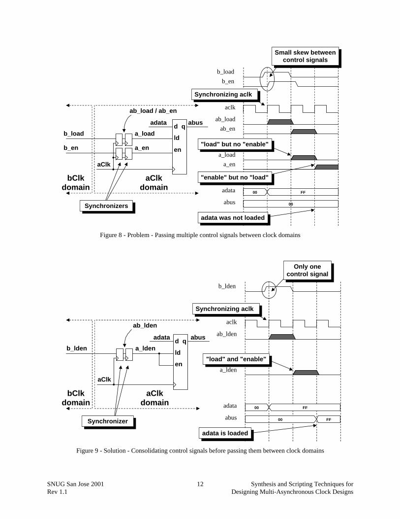
9.1 Problem - Two simultaneously required control signals.
In the simple example shown in Figure 8, a register in the new clock domain requires both a loadsignal and an enable signal in order to load a data value into the register. If both the load andenable signals are being sent from one clock domain, there is a chance that a small skew betweenthe control signals could cause the two signals to be synchronized into different clock cycleswithin the new clock domain. In this example, this would cause the data to the register to not beloaded.
SNUG San Jose 2001 Synthesis and Scripting Techniques forRev 1.1 Designing Multi-Asynchronous Clock Designs
12
b_load
aClk
bClkdomain
aClkdomain
a_load
ab_load / ab_en
b_en a_en
Synchronizers
abusadata
en
ld
d q
00
00 FF
b_load
ab_load
b_en
ab_en
a_load
a_en
adata
abus
aclk
Small skew betweencontrol signals
"enable" but no "load"
"load" but no "enable"
adata was not loaded
Synchronizing aclk
Figure 8 - Problem - Passing multiple control signals between clock domains
FF
FF
b_lden
aClk
bClkdomain
aClkdomain
a_lden
ab_lden
Synchronizer
abusadata
en
ld
d q
00
00
b_lden
ab_lden
a_lden
adata
abus
aclk
"load" and "enable"
adata is loaded
Only onecontrol signal
Synchronizing aclk
Figure 9 - Solution - Consolidating control signals before passing them between clock domains

SNUG San Jose 2001 Synthesis and Scripting Techniques forRev 1.1 Designing Multi-Asynchronous Clock Designs
13
The solution to the problem in this simple example is easy. As shown in Figure 9, drive both theload and enable register input signals in the new clock domain from just one control signal. Thiswill remove the potential for the control signals arriving shifted in time.
9.2 Problem - Two phase-shifted sequencing control signals.
The diagram in Figure 10, shows two enable signals, aen1 and aen2, that are used to enable thesequential passing of a data signal through a short pipeline design. The problem is that in the firstclock domain, the aen1 control signal might terminate slightly before the aen2 control signal isasserted, and the second clock domain might try to sample the aen1 and aen2 control signals inthe middle of this slight time gap, causing a one-cycle gap to form in the enable control-signalchain in the second clock domain. This would cause the a2 output signal to be missed by thesecond flip-flop.
ben1
aClk
bClkdomain
aClkdomain
aen1
ab_en1 / ab_en2
ben2 aen2
a3q q
a2a1
Synchronizers
ben1
ab_en1
ben2
ab_en2
aen1
aen2
a1
a2
aclk
a3
2nd enable signal is too late
a3 was not loaded
Small skew betweencontrol signals
Synchronizing aclk
Figure 10 - Problem - Passing sequential control signals between clock domains
The solution to the problem, as shown in Figure 11, is to send only one control signal into thenew clock domain and generate the second phase-shifted sequential control signal within the newclock domain.

SNUG San Jose 2001 Synthesis and Scripting Techniques forRev 1.1 Designing Multi-Asynchronous Clock Designs
14
Synchronizers
ben1
aClk
bClkdomain
aClkdomain
aen1
ab_en1
aen2
a3q q
a2a1
a3 loaded
Synchronizing aclk
ben1
ab_en1
aen1
aen2
a1
a2
aclk
a3
Only onecontrol signal
Figure 11 - Solution - Logic to generate the proper sequencing signals in the new clock domains
9.3 Problem - Two encoded control signals.
bdec[1]
aClk
bClkdomain
aClkdomain
adec[1]
ab_dec[1:0]
aen[3]
aen[2]
aen[1]
aen[0]
bdec[0] adec[0]
Synchronizers WRONG!aen[2] should not
be asserted
bdec[1]
ab_dec[1]
bdec[0]
ab_dec[0]
adec[1]
adec[0]
aen[3]
aen[2]
aen[1]
aen[0]
aen[0] aen[0] aen[2] aen[3]
bdec=0 bdec=3
aclk
Figure 12 - Problem - Encoded control signals passed between clock domains

SNUG San Jose 2001 Synthesis and Scripting Techniques forRev 1.1 Designing Multi-Asynchronous Clock Designs
15
The diagram in Figure 12 shows two encoded control signals being passed between clockdomains. If the two encoded signals are slightly skewed when sampled, an erroneous decodedoutput could be generated for one clock period in the new clock domain.
One potential solution to this problem, as shown in Figure 13, is to send a shaped enable signalto act as a "ready flag" in the new clock domain. The sending clock domain must generate andenable signal one clock cycle after asserting the decoder inputs. The sending clock domain mustalso remove the enable signal one clock cycle before de-asserting the decoder inputs. Asdescribed earlier, the enable signal must be asserted for a time period that is longer than the cycletime of the receiving clock domain.
Shaped enablepulse
Synchronizers
en
bdec[1]
aClkbClk
domain
adec[1]
ab_dec[1:0]
aen[3]
aen[2]
aen[1]
aen[0]
bdec[0] adec[0]
bden_n aden_n
aClkdomain
bdec[1]
bden_n
ab_dec[1]
bdec[0]
ab_dec[0]
adec[1]
adec[0]
aen[3]
aen[2]
aen[1]
aen[0]
bdec=0 bdec=3
aclk
ab_den_n
aden_n
aen[3]
"1" (off)
"1" (off)
"1" (off)
"1" (off)
Figure 13 - Solution #1 - Logic to synchronize and wave-shape an enable pulse to pass between clock domains
Under worst case conditions, the shaped enable signal will either be sampled at the same time asthe encoded inputs are sampled into the receiving clock domain, or the shaped enable signal willbe de-asserted at the same time as the encoded inputs are de-asserted in the receiving clockdomain. Under best case conditions, the shaped enable pulse will be asserted one receiving clockcycle later than the assertion of the encoded inputs and de-asserted one receiving clock cyclebefore the de-assertion of the encoded inputs. This method insures that the encoded inputs arevalid before they are enabled into the receiving clock domain.
A second potential solution to this problem, as shown in Figure 14, is to decode the signals backin the sending clock domain and then send the decoded outputs (where only one of the outputs isasserted) through synchronizers into the new clock domain. Within the new clock domain, a statemachine is used to determine when a new decoded output has been asserted. If there are nodecoded outputs, it means that one decoded output has been de-asserted and that another decoded

SNUG San Jose 2001 Synthesis and Scripting Techniques forRev 1.1 Designing Multi-Asynchronous Clock Designs
16
output is about to be asserted. If there are two asserted decoded output signals, the last decodedoutput signal will cause the state machine to change states and the older decoded output signalwill turn off on the next rising clock edge in the new clock domain. It is important that the senderinsure that the decoded outputs are each asserted for a time period that is longer than the cycletime of the receiving clock domain.
!aen[2]Synchronizers
a_sel3
a_sel2
a_sel1
a_sel0
ben[3]
ben[2]
ben[1]
ben[0]
bdec[1]
bClk
bClkdomain
ab_ en[3:0]
bdec[0]
aClkdomain
aClk
aen[3]
aen[2]
aen[1]
aen[0]
!aen[2]
!aen[3]
!aen[1]
!aen[0]!arst_n
!aen[1]
!aen[1]
!aen[0]
!aen[0]
!aen[2]
!aen[3]
!aen[3]
EN0!a_sel0
EN1!a_sel1
EN2!a_sel2
EN3!a_sel3
Except where noted, the following outputsare driven to the default, de-asserted state:a_sel3=1, a_sel2=1, a_sel1=1, a_sel0=1
Figure 14 - Solution #2 - FSM logic to detect one-hot control signals passed from a different clock domain
Any time there are multiple control signals crossing clock boundaries, caution must be taken toinsure that the sequencing of the control signals being passed is correct or that any potential mis-sequencing of the control signals will not adversely impact the correct operation of the design.
10.0 Data-Path Synchronization
Passing data from one clock domain to another is an example of passing multiple randomlychanging signals between clock domains. Using synchronizers to handle the passing of data isgenerally unacceptable. There are far too many opportunities for multi-bit data changes to beincorrectly sampled using synchronizers.
Two common methods for synchronizing data between clock domains are: (1) use handshakesignals to pass data between clock domains or, (2) use FIFOs (First In First Out memories) tostore data using one clock domain and to retrieve data using another clock domain.
10.1 Handshaking Data Between Clock Domains
Data can be passed between clock domains using two or three handshake control signals,depending on the application and the paranoia of the design engineer. When it comes tohandshaking, the more control signals that are used, the longer the latency to pass data from one
SNUG San Jose 2001 Synthesis and Scripting Techniques forRev 1.1 Designing Multi-Asynchronous Clock Designs
17
clock domain to another. The biggest disadvantage to using handshaking is the latency requiredto pass and recognize all of the handshaking signals for each data word that is transferred.
For many open-ended data-passing applications, a simple two-line handshaking sequence issufficient. The sender places data onto a data bus and then synchronizes a "data_valid" signal tothe receiving clock domain. When the "data_valid" signal is recognized in the new clock domain,the receiver clocks the data into a register in the new clock domain (the data should have beenstable for at least two rising clock edges in the sending clock domain) and then passes an"acknowledge" signal through a synchronizer to the sender. When the sender recognizes thesynchronized "acknowledge" signal, the sender can change the value being driven onto the databus.
Under some circumstances, it might be useful to use a third control signal, "ready", sent througha synchronizer from the receiver to the sender to indicate that the receiver is indeed "ready" toreceive data. The "ready" signal should not be asserted while the "data_valid" signal is true.When the "data_valid" signal is de-asserted, a "ready" signal can be passed to the sender. Ofcourse, with the added handshake signal comes the penalty of longer latency to synchronize andrecognize the third control signal.
10.2 Passing Data By FIFO Between Clock Domains
One of the most popular methods of passing data between clock domains is to use a FIFO. A dualport memory is used for the FIFO storage. One port is controlled by the sender which puts datainto the memory as fast a one data word (or one data bit for serial applications) per write clock.The other port is controlled by the receiver, which pulls data out of memory one data word perread clock. Two control signals are used to indicate if the FIFO is empty, full or partially full.Two additional control signals are frequently used to indicate if the FIFO is almost full or almostempty.
In theory, placing data into a shared memory with one clock and removing the data from theshared memory with another clock seems like an easy and ideal solution to passing data betweenclock domains. For the most part it is, but generating accurate full and empty flags can bechallenging.
10.3 FIFO Full & Empty
Determining that a FIFO is full or empty requires some type of mathematical manipulationand/or comparison of write and read pointers. The problem is that the two pointers are generatedin two different clock domains, so one or both pointers must be synchronized into the oppositeclock domain before mathematical and comparison operations can be safely performed.
10.4 FIFO Pointers - Implemented as Binary Counters
Any FIFO pointer that must be synchronized into a different clock domain should not beimplemented as a binary counter.

SNUG San Jose 2001 Synthesis and Scripting Techniques forRev 1.1 Designing Multi-Asynchronous Clock Designs
18
One characteristic of binary counters is that half of all sequential binary incrementing operationsrequire that two or more counter bits must change. Trying to synchronize a binary counter into anew clock domain is more problematic than trying to synchronize multiple control signals into anew clock domain. If a simple 4-bit binary counter changes from address 7 (binary 0111) toaddress 8 (binary 1000), all four counter bits will change at the same time. If a synchronizingclock edge comes in the middle of this transition, it is possible that any 4-bit binary pattern couldbe sampled and synchronized into the new clock domain as shown in Figure 15.
Binary CountValues
00 0 0 0 001 0 0 0 102 0 0 1 003 0 0 1 104 0 1 0 005 0 1 0 106 0 1 1 007 0 1 1 108 1 0 0 009 1 0 0 110 1 0 1 011 1 0 1 112 1 1 0 013 1 1 0 114 1 1 1 015 1 1 1 1
07 -> 08 possible binary transitions0 1 1 1 -> 1 0 0 0 (07->08)
0 1 1 1 -> 0 0 0 0 (07->00)0 1 1 1 -> 0 0 0 1 (07->01)0 1 1 1 -> 0 0 1 0 (07->02)0 1 1 1 -> 0 0 1 1 (07->03)0 1 1 1 -> 0 1 0 0 (07->04)0 1 1 1 -> 0 1 0 1 (07->05)0 1 1 1 -> 0 1 1 0 (07->06)0 1 1 1 -> 0 1 1 1 (07->07)0 1 1 1 -> 1 0 0 0 (07->08)0 1 1 1 -> 1 0 0 1 (07->09)0 1 1 1 -> 1 0 1 0 (07->10)0 1 1 1 -> 1 0 1 1 (07->11)0 1 1 1 -> 1 1 0 0 (07->12)0 1 1 1 -> 1 1 0 1 (07->13)0 1 1 1 -> 1 1 1 0 (07->14)0 1 1 1 -> 1 1 1 1 (07->15)
Figure 15 - Binary count values sampled in mid-transition
The new, synchronized binary value might trigger a false full or empty flag, or even worse, itmight not trigger a real full or empty flag causing data to be lost due to FIFO overflow or causingbogus data to be read from the FIFO due to attempting to read data when the FIFO is reallyempty.
10.5 FIFO Pointers - Implemented as Gray-Code Counters
Although binary counters work fine for addressing the memory, trying to synchronize binarycounters into a new clock domain is problematic. A better approach for passing pointers betweenclock domains is to use a gray-code counter for the two FIFO pointers. Gray code counters onlychange one bit at a time. If a synchronizing clock signal comes in the middle of a gray codecounter transition, the synchronized value will either be the old value or the new value becauseonly one bit is changing at a time.

SNUG San Jose 2001 Synthesis and Scripting Techniques forRev 1.1 Designing Multi-Asynchronous Clock Designs
19
10.6 Designing Gray Code Counters
A block diagram for a gray-code counter is shown in Figure 16. To design a gray code counter, aregister is used to store the gray code values. The register output is fed back to a gray-to-binaryconverter, the binary value is incremented by one, the incremented binary value is then passed toa binary-to-gray converter that drives the inputs to the gray-code register.
Binaryto Graycomb.logic
GrayCodereg
The gray andbinary values
increment onlyif inc is high
The bnext output isthe binary value +1
(if inc is high)
inc
bingnext graybnext d
rst_n
q
rst_n
clk
+
Gray toBinarycomb.logic
For-loop with twolines of code
One lineof code
One line of codewith concatenations
Figure 16 - Gray-code counter block diagram
10.7 Gray To Binary Conversion
To convert a gray-code value to an equivalent binary-code value, using an n-bit gray code valueas an example, binary bit 0 is equal to the exclusive-or of gray code bit 0 exclusive-ored with allother gray code bits from 1 to n. Binary bit 1 is equal gray code bit 1 exclusive-ored with allother gray code bits from 2 to n, etc. The most significant binary bit is just equal to the mostsignificant gray code bit. The equations for a 4-bit gray-to-binary conversion are shown in Figure17.
bin[0] = gray[3] ^ gray[2] ^ gray[1] ^ gray[0];bin[1] = gray[3] ^ gray[2] ^ gray[1];bin[2] = gray[3] ^ gray[2];bin[3] = gray[3];
Figure 17 - 4-bit gray-to-binary conversion equations
The easiest way to code a gray-to-binary converter is to code a for-loop and do an exclusive-orreduction on a gray code vector with variable index range, where each time through the loop the

SNUG San Jose 2001 Synthesis and Scripting Techniques forRev 1.1 Designing Multi-Asynchronous Clock Designs
20
LSB of the index range increases until we are left with a simple assignment of bin[MSB] =^gray[MSB:MSB] (just the 1-bit MSB of the gray code vector), as shown in Example 1.
module gray2bin_bad (bin, gray); parameter SIZE = 4; output [SIZE-1:0] bin; input [SIZE-1:0] gray; reg [SIZE-1:0] bin; integer i;
// Syntax Error - variable index range always @(gray) for (i=0; i<SIZE; i=i+1) bin[i] = ^(gray[SIZE-1:i]);endmodule
Example 1 - Non-working but conceptually correct gray-to-binary Verilog model
Unfortunately, Verilog does not permit part selects using a variable index range so the code inExample 1, although conceptually correct, will not compile.
Another way to think of a gray-to-binary conversion is to exclusive-or the significant gray-codebits with padded 0's as shown in Figure 18.
bin[0] = gray[3] ^ gray[2] ^ gray[1] ^ gray[0] ; // gray>>0bin[1] = 1'b0 ^ gray[3] ^ gray[2] ^ gray[1] ; // gray>>1bin[2] = 1'b0 ^ 1'b0 ^ gray[3] ^ gray[2] ; // gray>>2bin[3] = 1'b0 ^ 1'b0 ^ 1'b0 ^ gray[3] ; // gray>>3
Figure 18 - 4-bit gray-to-binary conversion equations - 2nd method
The corresponding parameterized Verilog model for this algorithm is shown in Example 2. Thisexample is syntactically correct, will compile and does work.
module gray2bin (bin, gray); parameter SIZE = 4; output [SIZE-1:0] bin; input [SIZE-1:0] gray; reg [SIZE-1:0] bin; integer i;
always @(gray) for (i=0; i<SIZE; i=i+1) bin[i] = ^(gray>>i);endmodule
Example 2 - Parameterized and correct gray-to-binary Verilog model
10.8 Binary To Gray Conversion
To convert a binary value to an equivalent gray-code value, using an n-bit binary value as anexample, gray-code bit 0 is equal to the exclusive-or of binary bits 0 and 1. Gray-code bit 1 is

SNUG San Jose 2001 Synthesis and Scripting Techniques forRev 1.1 Designing Multi-Asynchronous Clock Designs
21
equal to the exclusive-or of binary bits 1 and 2, etc. The most significant gray-code bit is justequal to the most significant binary bit. The equations for a 4-bit binary-to-gray conversion areshown in Figure 19.
bin[0] = gray[0] ^ gray[1];bin[1] = gray[1] ^ gray[2];bin[2] = gray[2] ^ gray[3];bin[3] = gray[3];
Figure 19 - 4-bit binary-to-gray conversion equations
The easiest way to code a binary-to-gray converter is to code a simple continuous assignment thatperforms a bit-wise exclusive-or operation between the binary vector and a right-shifted versionof the same binary vector as shown in Example 3. This example is syntactically correct, willcompile and does work.
module bin2gray (gray, bin); parameter SIZE = 4; output [SIZE-1:0] gray; input [SIZE-1:0] bin;
assign gray = (bin>>1) ^ bin;endmodule
Example 3 - Parameterized binary-to-gray Verilog model
10.9 Gray Code Counter
The Verilog code for a gray-code counter incorporates a gray-to-binary converter, a binary-to-gray converter and increments the binary value between conversions. The parameterized Verilogmodel for the gray-code counter is shown in Example 4.
module graycntr (gray, clk, inc, rst_n); parameter SIZE = 4; output [SIZE-1:0] gray; input clk, inc, rst_n; reg [SIZE-1:0] gnext, gray, bnext, bin; integer i;
always @(posedge clk or negedge rst_n) if (!rst_n) gray <= 0; else gray <= gnext;
always @(gray or inc) begin for (i=0; i<SIZE; i=i+1) bin[i] = ^(gray>>i); bnext = bin + inc; gnext = (bnext>>1) ^ bnext; endendmodule
Example 4 - Parameterized gray-code counter Verilog model
SNUG San Jose 2001 Synthesis and Scripting Techniques forRev 1.1 Designing Multi-Asynchronous Clock Designs
22
11.0 FIFO Design
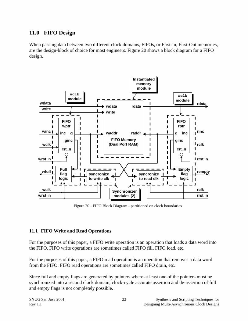
When passing data between two different clock domains, FIFOs, or First-In, First-Out memories,are the design-block of choice for most engineers. Figure 20 shows a block diagram for a FIFOdesign.
wfull remptyEmptyflag
logic
Fullflaglogic
FIFO Memory(Dual Port RAM)
write
waddr
wdata
raddr
rdata
winc
wclk
wrst_n
FIFOwptr
rst_n
inc g
ginc
rinc
rclk
rrst_n
syncronizeto read clk
syncronizeto write clk
FIFOrptr
rst_n
incg
ginc
write
wdata
wclkwrst_n
rclkrrst_n
rdata
rclkmodule
wclkmodule
Instantiatedmemorymodule
Synchronizermodules (2)
Figure 20 - FIFO Block Diagram - partitioned on clock boundaries
11.1 FIFO Write and Read Operations
For the purposes of this paper, a FIFO write operation is an operation that loads a data word intothe FIFO. FIFO write operations are sometimes called FIFO fill, FIFO load, etc.
For the purposes of this paper, a FIFO read operation is an operation that removes a data wordfrom the FIFO. FIFO read operations are sometimes called FIFO drain, etc.
Since full and empty flags are generated by pointers where at least one of the pointers must besynchronized into a second clock domain, clock-cycle accurate assertion and de-assertion of fulland empty flags is not completely possible.

SNUG San Jose 2001 Synthesis and Scripting Techniques forRev 1.1 Designing Multi-Asynchronous Clock Designs
23
One FIFO design technique is to insure that a full or empty flag is asserted exactly when full orempty conditions occur, but de-asserting the flags might come a few clock cycles late. This issometimes referred to as pessimistic full and empty flags.
11.2 Pessimistic full and empty flags
A pessimistic full flag is a full signal that is asserted immediately when a FIFO becomes full butis de-asserted late (it is not de-asserted until a few read-clock cycles later).
Because the write pointer does not have to be synchronized before testing for a full condition, thefull flag will be asserted immediately when the FIFO goes full. The FIFO might not actually becompletely full because the read pointer might have incremented but the new read pointer valuemight not have been synchronized into the write clock domain. Using the block diagram shownin Figure 20, the read pointer synchronized into the write clock domain is always two writeclocks behind the actual read pointer value, so the full flag might be asserted for two extra writeclocks. This typically is not a problem since the full flag is simply holding off transmission ofmore data from the data sending source for two extra write clock cycles. Pointers beingsynchronized into a new clock domain should be gray code counters for reasons explained insections 10.4 and section 10.5.
Similarly, because the read pointer does not have to be synchronized before testing for an emptycondition, the empty flag will be asserted immediately when the FIFO goes empty. The FIFOmight not actually be completely empty because the write pointer might have incremented but thenew write pointer value might not have been synchronized into the read clock domain. Using theblock diagram shown in Figure 20, the write pointer synchronized into the read clock domain isalways two read clocks behind the actual write pointer value, so the empty flag might be assertedfor two extra read clocks. This typically is not a problem since the empty flag is merelyinforming the data receiver that data is not ready to be sent for another two read clock cycles.Again, pointers being synchronized into a new clock domain should be gray code counters forreasons explained in sections 10.4 and section 10.5.
11.3 Full & Empty
A FIFO is full when both pointers are equal. A FIFO is also empty when both pointers are equal,so the FIFO pointers should be one bit larger than is necessary to address the full memory range.The extra bit is used as a flag to help determine if the FIFO is empty or full. If the extra, pointerMSBs are equal, it means that the FIFO pointers have wrapped back to address 0 an equalnumber of times and if the rest of the FIFO bits are equal, the FIFO is empty. If the extra, pointerMSBs are not equal, it means that the write pointer has wrapped back to address 0 one more timethan the read pointer and if the rest of the FIFO bits are equal, the FIFO is full.

SNUG San Jose 2001 Synthesis and Scripting Techniques forRev 1.1 Designing Multi-Asynchronous Clock Designs
24
12.0 Simulation Issues
As mentioned in section 4.0, signals crossing clock boundaries through a synchronizer willexperience setup and hold violations. That is why synchronizers are added to a design, to filterout the metastability effects of a signal that changes too close to the rising edge of a new clockdomain clock signal.
When doing gate-level simulations on a multi-clock design, the ASIC library models of flip-flopsare modeled with setup and hold time expressions to match the timing specifications of the actualflip-flops. ASIC libraries typically model flip-flops to drive X's (unknowns) on the flip-flopoutputs when a timing violation occurs. When simulating gate-level synchronizers, setup andhold time violations might cause ASIC libraries to issue setup and hold time error messages andthe offending signals are frequently driven to an X value. These X-values propagate to the rest ofthe design causing problems when trying to verify the functionality of the entire gate-leveldesign.
Most Verilog simulators have a command option to ignore all timing checks, but this would alsoignore the desired timing checks for the rest of the design.
It is possible to change the setup and hold time setting to zero for any ASIC library flip-flop thatis used in a synchronizer, but that would cause all setup and hold time checks of all instances ofthat same type of flip-flop to be set to zero, including the flip-flops that you might want to use totest the rest of the design.
You could make copies of flip-flops from an ASIC library and store them into a new Veriloglibrary with different names, set to zero all setup and hold times, then modify the design gate-level netlist, replacing all first stage synchronizer ASIC library flip-flops with the modifiedlibrary flip-flops without timing checks, but this could be an error prone and tedious process thatmight have to be repeated each time a new netlist is generated or it might require the creation of amakefile and scripts to automatically make the modifications each time a new netlist isgenerated.
A clever way to approach this problem suggested by Bhatnagar[7] is to use Synopsys commandsto modify the SDF backannotation of the setup and hold time on just the first stage flip-flop cellsin the design. Bhatnagar points out that the SDF file is instance based and therefore targeting thesetup and hold times for the offending cells is more easily accomplished. Bhatnagar notes:
Instead of manually removing the setup and hold-time constructs from the SDF file, abetter way is to zero out the setup and hold-times in the SDF file, only for theviolating flops, i.e., replace the existing setup and hold-time numbers with zero's.
Bhatnagar further points out that setup hold times of zero means that there can be no timingviolation, therefore no unknowns propagated to the rest of the design. The following dc_shellcommand, given by Bhatnagar, is used to make setup and hold times zero:

SNUG San Jose 2001 Synthesis and Scripting Techniques forRev 1.1 Designing Multi-Asynchronous Clock Designs
25
set_annotated_check 0 -setup -hold -from REG1/CLK -to REG1/D
Using a creative naming convention for the output of the first stage flip-flop of a synchronizermight make wild card expressions possible to easily backannotate all first stage flip-flop SDFsetup and hold time values to zero using very few dc_shell commands.
13.0 Conclusions
Completely synchronous one-clock design techniques are well known. Synthesis tools do theirbest work on synchronous designs. Timing analysis tools are designed to report timing problemson one-clock synchronous designs. Synthesis scripts are easy to create for one-clock synchronousclock designs. The techniques in this paper are aimed at making the design look like multiplesingle clock designs!
• Partitioning non-synchronizer blocks so that there is only one clock per module permitseasy verification of correct timing by creating clock-domain sub-blocks that can be moreeasily verified with static timing analysis tools.
• Partitioning synchronizer blocks to permit inputs from one and only one clock domain andclocking the signals with only one asynchronous clock creates manageable synchronizer sub-blocks that can also be easily timed.
• A clock-oriented naming convention can be useful to help identify signals that need to betimed within the different asynchronous clock domains.
• Multiple control signals crossing clock domains require special attention to ensure that allcontrol signals are properly sequenced into a new clock domain.
The techniques described in this paper were developed to facilitate robust development andverification of multi-clock designs.
References
[1] William J. Dally and John W. Poulton, Digital Systems Engineering, CambridgeUniversity Press, 1998, pg. 468.
[2] William J. Dally and John W. Poulton, Digital Systems Engineering, CambridgeUniversity Press, 1998, pp. 462-513.
[3] William J. Dally and John W. Poulton, Digital Systems Engineering, CambridgeUniversity Press, 1998, pp. 469-470.

SNUG San Jose 2001 Synthesis and Scripting Techniques forRev 1.1 Designing Multi-Asynchronous Clock Designs
26
[4] Samir Palnitkar, Verilog HDL, A Guide to Digital Design and Synthesis, Sunsoft Press APrentice Hall Title, 1996, pg. 193.
[5] Steve Golson, personal communication.
[6] ESNUG #281 - http://www.deepchip.com/posts/0281.html
[7] Himanshu Bhatnagar, Advanced ASIC Chip Synthesis, Kluwer Academic Publishers,1999, pp. 202-203.
Synopsys is a registered trademark of Synopsys, Inc.
Design Analyzer, DesignTime, PrimeTime and Synopsys Design Compiler are trademarks ofSynopsys, Inc.
Author & Contact Information
Cliff Cummings, President of Sunburst Design, Inc., is an independent EDA consultant andtrainer with 19 years of ASIC, FPGA and system design experience and nine years of Verilog,synthesis and methodology training experience.
Mr. Cummings, a member of the IEEE 1364 Verilog Standards Group (VSG) since 1994, chairedthe VSG Behavioral Task Force, which was charged with proposing enhancements to the Veriloglanguage. Mr. Cummings is also a member of the IEEE Verilog Synthesis InteroperabilityWorking Group.
Mr. Cummings holds a BSEE from Brigham Young University and an MSEE from Oregon StateUniversity.
E-mail Address: [email protected] paper can be downloaded from the web site: www.sunburst-design.com/papers
(Data accurate as of March 7th, 2001)