synthesis and scripting techniques for designing multi ... · pdf filesynthesis and scripting...
TRANSCRIPT
Expert Verilog, SystemVerilog & Synthesis Training
Synthesis and Scripting Techniques for Designing Multi-Asynchronous Clock Designs
Clifford E. Cummings, Sunburst Design, [email protected]
ABSTRACT
Designing a pure, one-clock synchronous design is a luxury that few ASIC designers will ever know. Most of theASICs that are ever designed are driven by multiple asynchronous clocks and require special data, control-signaland verification handling to insure the timely completion of a robust working design.
SNUG-2001San Jose, CA
Voted Best Paper3rd Place
SNUG San Jose 2001 Synthesis and Scripting Techniques for
Rev 1.2 Designing Multi-Asynchronous Clock Designs
2
1.0 IntroductionMost college courses teach engineering students prescribed techniques for designing completely synchronous(single clock) logic. In the real ASIC design world, there are very few single clock designs. This paper will detailsome of the hardware design, timing analysis, synthesis and simulation methodologies to address multi-clockdesigns.
This paper is not intended to provide exhaustive coverage of this topic, but is presented to share techniques learnedfrom experience.
2.0 MetastabilityQuoting from Dally and Poulton's book[6] concerning metastability:
"When sampling a changing data signal with a clock ... the order of the events determines the outcome.The smaller the time difference between the events, the longer it takes to determine which came first.When two events occur very close together, the decision process can take longer than the time allotted,and a synchronization failure occurs."
Datachanging
bclk samples adatwhile it is changing
aclkbclk
datadat bdat1
adat
bdat1
aclk
bclk
Clocked signal isinitially metastable ...
... and might still bemetastable at the next
rising edge of bclk
aclk isasynchronous
to bclk
Only onesynchronizing flip-flop
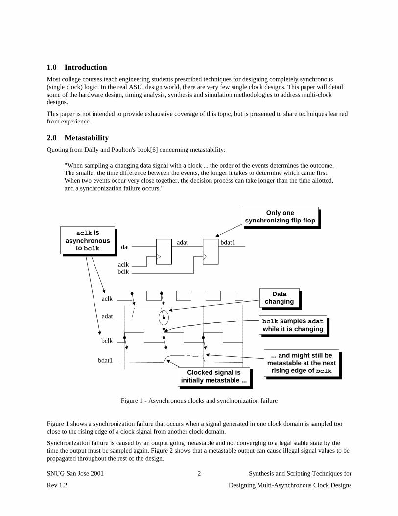
Figure 1 - Asynchronous clocks and synchronization failure
Figure 1 shows a synchronization failure that occurs when a signal generated in one clock domain is sampled tooclose to the rising edge of a clock signal from another clock domain.
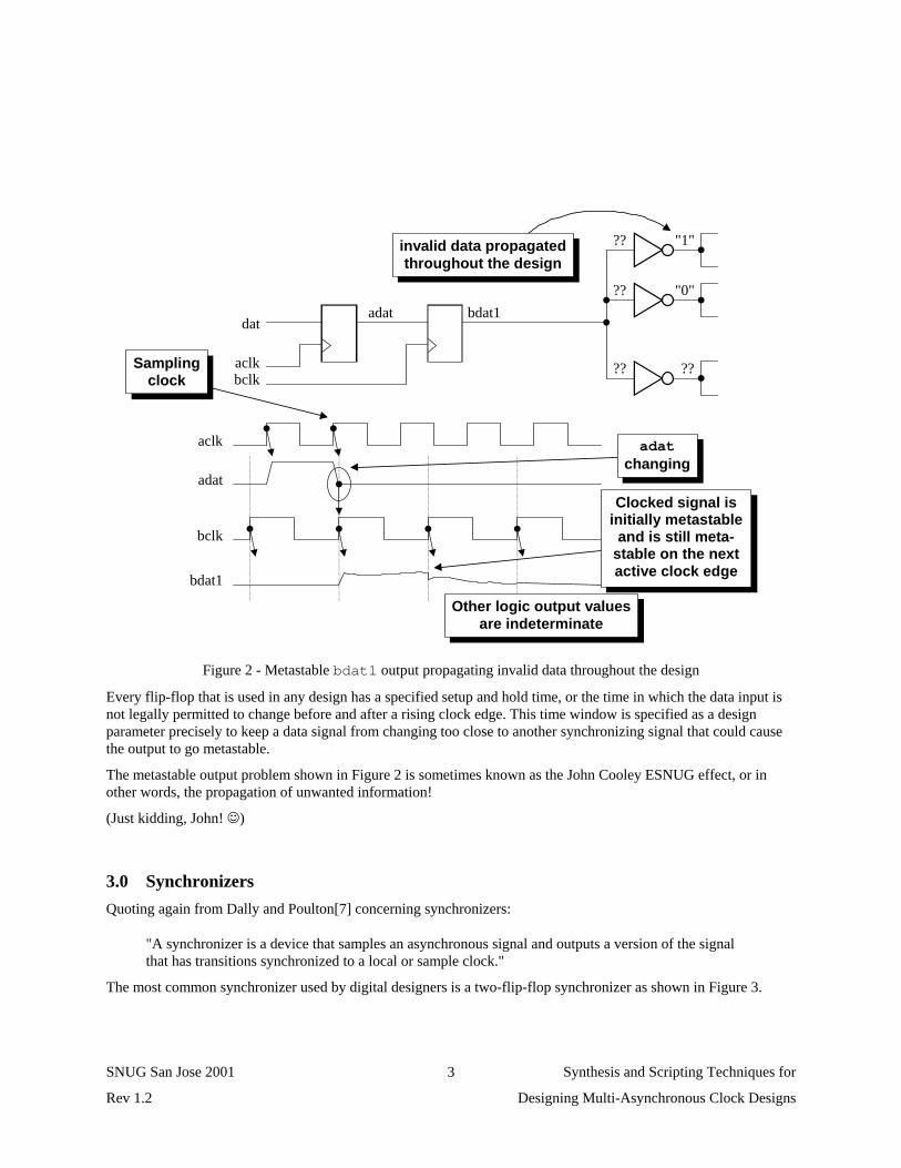
Synchronization failure is caused by an output going metastable and not converging to a legal stable state by thetime the output must be sampled again. Figure 2 shows that a metastable output can cause illegal signal values to bepropagated throughout the rest of the design.
SNUG San Jose 2001 Synthesis and Scripting Techniques for
Rev 1.2 Designing Multi-Asynchronous Clock Designs
3
aclkbclk
datadat bdat1
adat
bdat1
aclk
bclk
"1"
"0"
????
??
??
adatchanging
Samplingclock
Clocked signal isinitially metastable
and is still meta-stable on the nextactive clock edge
Other logic output valuesare indeterminate
invalid data propagatedthroughout the design
Figure 2 - Metastable bdat1 output propagating invalid data throughout the design
Every flip-flop that is used in any design has a specified setup and hold time, or the time in which the data input isnot legally permitted to change before and after a rising clock edge. This time window is specified as a designparameter precisely to keep a data signal from changing too close to another synchronizing signal that could causethe output to go metastable.
The metastable output problem shown in Figure 2 is sometimes known as the John Cooley ESNUG effect, or inother words, the propagation of unwanted information!
(Just kidding, John! ☺)
3.0 SynchronizersQuoting again from Dally and Poulton[7] concerning synchronizers:
"A synchronizer is a device that samples an asynchronous signal and outputs a version of the signalthat has transitions synchronized to a local or sample clock."
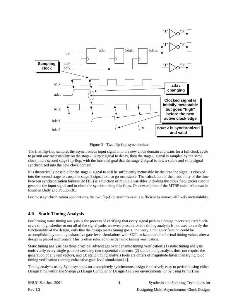
The most common synchronizer used by digital designers is a two-flip-flop synchronizer as shown in Figure 3.
SNUG San Jose 2001 Synthesis and Scripting Techniques for
Rev 1.2 Designing Multi-Asynchronous Clock Designs
4
aclkbclk
datadat bdat1 bdat2
adat
bdat1
bdat2
aclk
bclk
"0"
"0"
"0""1"
"1"
"1"
adatchanging
Samplingclock
Clocked signal isinitially metastable
but goes "high"before the next
active clock edge
bdat2 is synchronizedand valid
Figure 3 - Two flip-flop synchronizer
The first flip-flop samples the asynchronous input signal into the new clock domain and waits for a full clock cycleto permit any metastability on the stage-1 output signal to decay, then the stage-1 signal is sampled by the sameclock into a second stage flip-flop, with the intended goal that the stage-2 signal is now a stable and valid signalsynchronized into the new clock domain.
It is theoretically possible for the stage-1 signal to still be sufficiently metastable by the time the signal is clockedinto the second stage to cause the stage-2 signal to also go metastable. The calculation of the probability of the timebetween synchronization failures (MTBF) is a function of multiple variables including the clock frequencies used togenerate the input signal and to clock the synchronizing flip-flops. One description of the MTBF calculation can befound in Dally and Poulton[8].
For most synchronization applications, the two flip-flop synchronizer is sufficient to remove all likely metastability.
4.0 Static Timing AnalysisPerforming static timing analysis is the process of verifying that every signal path in a design meets required clock-cycle timing, whether or not all of the signal paths are even possible. Static timing analysis is not used to verify thefunctionality of the design, only that the design meets timing goals. In theory, timing verification could beaccomplished by running exhaustive gate-level simulations with SDF backannotation of actual timing values after adesign is placed and routed. This is often referred to as dynamic timing verification.
Static timing analysis has three principal advantages over dynamic timing verification: (1) static timing analysistools verify every single path between any two sequential elements, (2) static timing analysis does not require thegeneration of any test vectors, and (3) static timing analysis tools are orders of magnitude faster than trying to dotiming verification running exhaustive gate-level simulations[4].
Timing analysis using Synopsys tools on a completely synchronous design is relatively easy to perform using eitherDesignTime within the Synopsys Design Compiler or Design Analyzer environments, or by using PrimeTime.
SNUG San Jose 2001 Synthesis and Scripting Techniques for
Rev 1.2 Designing Multi-Asynchronous Clock Designs
5
Timing analysis on modules with two or more asynchronous clocks is error prone, more difficult and can be timeconsuming. Static timing analysis on signals generated from one clock domain and latched into sequential elementswithin a second, asynchronous clock domain is inaccurate and for the most part worthless. The timing informationfor a signal latched by a clock that is asynchronous to the latched signal is inaccurate because the phase relationshipbetween the signal and the asynchronous clock is always changing; therefore, the static timing analysis tool wouldhave to check an infinite number of phase relationships between the signal and asynchronous clock. The fact is, onemust assume that signals that pass from one clock domain to another at some point will violate either setup or holdtimes on the destination sequential element.
There is no good reason to perform timing analysis on signals that are generated in one clock domain and registeredin another asynchronous clock domain. It is a given that these signals DO violate setup and hold times on thedestination register. This is why synchronizers (see section 3.0) are needed, to alleviate the problems that can occurwhen a signal is passed from one clock domain to another.
For RTL modules that have two or more asynchronous clocks as inputs, a designer will be required to indicate to thestatic timing analysis tool which signal paths should be ignored. This is accomplished by "setting false paths" onsignals that cross from one clock domain to another. This can be a tedious and error prone job unless the guidelinesin the next two sections are followed.
5.0 Clock Naming ConventionsGuideline: Use a clock naming convention to identify the clock source of every signal in a design.
Reason: A naming convention helps all team members to identify the clock domain for every signal in a design andalso makes grouping of signals for timing analysis easier to do using regular expression "wild-carding" from withina synthesis script.
A number of useful clock naming conventions have been used by various design teams. One that was used bydesign engineers in 1995 while designing video ASICs for In Focus projectors required that a leading prefixcharacter be used to identify the various asynchronous clock domains. Examples included: uClk for themicroprocessor clock, vClk for the video clock and dClk for the display clock.
Each signal was synchronized to one of the clock domains in the design and each signal-name had to include aprefix character identifying the clock domain for that signal. Any signal that was clocked by the uClk would have au-prefix in the signal name, such as uaddr, udata, uwrite, etc. Any signal that was clocked by the vClk wouldsimilarly have a v-prefix in the signal name, such as vdata, vhsync, vframe, etc. The same signal naming conventionwas used for all signals generated by any of the other clocks in the design.
Using this technique, any engineer on the ASIC design team could easily identify the clock-domain source of anysignal in the design and either use the signals directly or pass the signals through a synchronizer so that they couldbe used within a new clock domain.
The naming convention alone contributed significantly to the productivity of the design team. How do we knowthere was a productivity gain? One of the design engineers started his part of the ASIC design using his own namingconvention, ignoring the convention in use by the other design team members. After much confusion about thesignals entering and leaving his design partition, a team meeting was called and the non-compliant designer was"strongly encouraged" to rename the signals in his part of the design to conform to the team naming convention.After the signal names were changed, it became easier to interface to the partition in question. Fewer questions andless confusions occurred after the change.
SNUG San Jose 2001 Synthesis and Scripting Techniques for
Rev 1.2 Designing Multi-Asynchronous Clock Designs
6
6.0 Design PartitioningGuideline: Only allow one clock per module.
Reason: Static timing analysis and creating synthesis scripts is more easily accomplished on single-clock modulesor groups of single-clock modules.
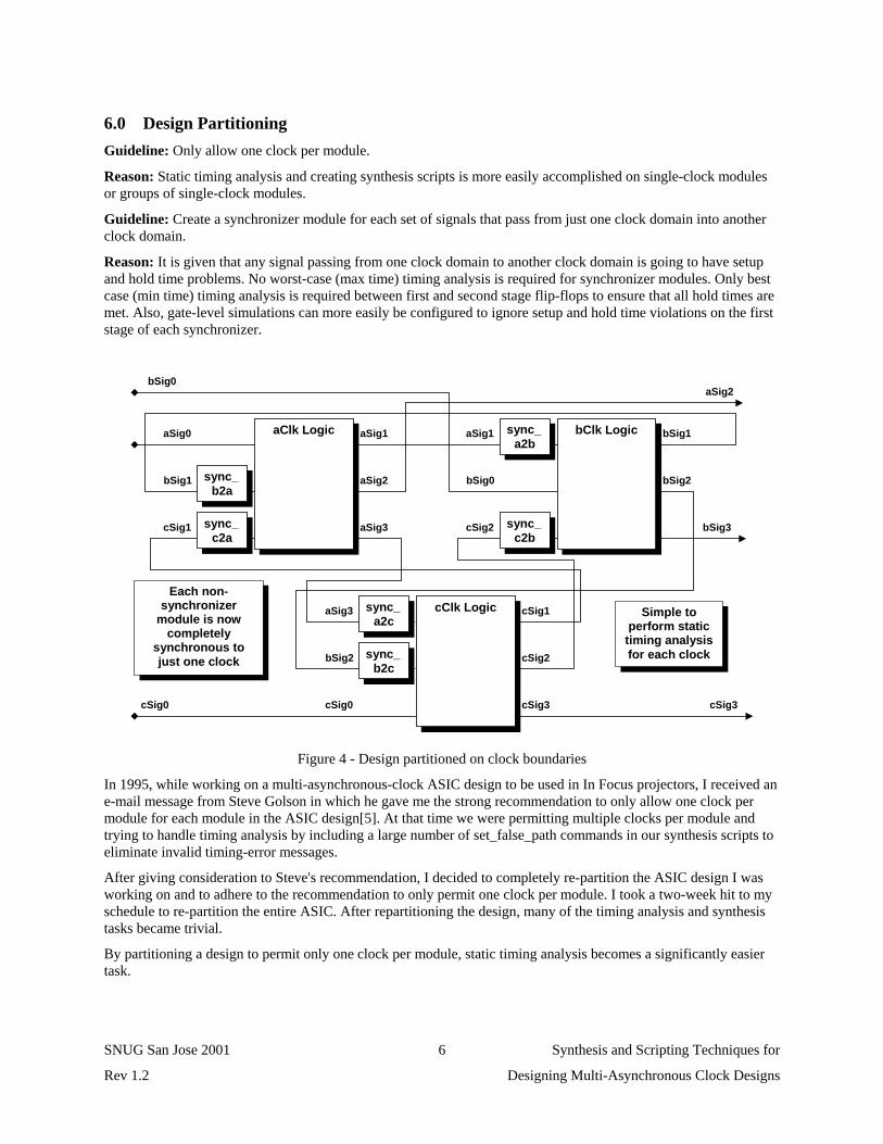
Guideline: Create a synchronizer module for each set of signals that pass from just one clock domain into anotherclock domain.
Reason: It is given that any signal passing from one clock domain to another clock domain is going to have setupand hold time problems. No worst-case (max time) timing analysis is required for synchronizer modules. Only bestcase (min time) timing analysis is required between first and second stage flip-flops to ensure that all hold times aremet. Also, gate-level simulations can more easily be configured to ignore setup and hold time violations on the firststage of each synchronizer.
aSig3
bSig2
cSig0
cSig1
cSig2
cSig3
cClk Logicsync_a2c
sync_b2c
aSig0
bSig1
cSig1
aSig1
aSig2
aSig3
aClk Logic
sync_b2a
sync_c2a
aSig1
bSig0
cSig2
bSig1
bSig2
bSig3
bClk Logicsync_a2b
sync_c2b
aSig2
cSig3
bSig0
cSig0
Each non-synchronizer
module is nowcompletely
synchronous tojust one clock
Simple toperform statictiming analysisfor each clock
Figure 4 - Design partitioned on clock boundaries
In 1995, while working on a multi-asynchronous-clock ASIC design to be used in In Focus projectors, I received ane-mail message from Steve Golson in which he gave me the strong recommendation to only allow one clock permodule for each module in the ASIC design[5]. At that time we were permitting multiple clocks per module andtrying to handle timing analysis by including a large number of set_false_path commands in our synthesis scripts toeliminate invalid timing-error messages.
After giving consideration to Steve's recommendation, I decided to completely re-partition the ASIC design I wasworking on and to adhere to the recommendation to only permit one clock per module. I took a two-week hit to myschedule to re-partition the entire ASIC. After repartitioning the design, many of the timing analysis and synthesistasks became trivial.
By partitioning a design to permit only one clock per module, static timing analysis becomes a significantly easiertask.
SNUG San Jose 2001 Synthesis and Scripting Techniques for
Rev 1.2 Designing Multi-Asynchronous Clock Designs
7
The next logical step was to partition the design so that every input module signal was already synchronized to thesame clock domain before entering the module. Why is this significant? If all signals entering and leaving themodule are synchronous to the clock used in the module, the design is now completely synchronous! Now the entiremodule can be static timing analyzed without any "false paths" and Design Compiler can be used to "group" all ofthe same-clock synchronous modules to perform complete, sequential static timing analysis within each clockdomain.
There is one exception to the above recommendation. Multi-clock designs require at least some RTL modules topass signals from one clock domain to modules that are clocked within a different clock domain. For the In FocusASIC designs, we created separate synchronizer modules that permitted signals from one and only one clockdomain to be passed into a module that synchronized the signals into a new clock domain.
Using the naming convention described in section 5.0, all processor-clock generated signals (u-signals) would beused as inputs to a module that might be clocked by the video clock. This module was called the "sync_u2v" moduleand the RTL code did nothing more than take each u-signal input and run it through a pair of flip-flops clocked byvClk. Aside from the vClk and reset inputs, every other input signal to the "sync_u2v" module had a "u" prefix andevery output signal from that same module had a "v" prefix.
No worst-case timing analysis is required on the "sync" modules because we know that every input signal to thesemodules will have timing problems; otherwise, we would not have to pass the signals through synchronizers. Theonly timing analysis that we need to perform within synchronizer modules is min-time (hold time) analysis betweenthe first and second flip-flop stages for each signal.
In general, if there are n asynchronous clock domains, the design will require n(n-1) synchronizer modules, two foreach pair of clock signals (example: using the uClk and vClk signals: the two synchronizer modules required wouldbe sync_u2v and sync_v2u). Only if there are no signals that pass between two specific clock domains will a pair ofsynchronizer modules not be required.
By the way, what happened to that repartitioned In Focus ASIC design? After modifying all of the RTL files tocreate either completely synchronous modules or synchronizer modules, the task of generating synthesis scriptsbecame trivial. All of the script files which previously included "set_false_path" commands were either deleted orsignificantly simplified. All timing problems were easily identified and fixed (because they were all within single-clock domain groupings) and the final synthesis runs completed two weeks earlier than anticipated, putting theproject back on schedule and completely justifying the decision to repartition the design.
7.0 Synthesis Scripts & Timing AnalysisFollowing the guidelines of section 6.0, to only permit one clock per module, to require that all signals enteringnon-synchronizer modules are also in the same clock domain that is used to clock that module and to require thatsynchronizer modules only permit input signals from one other clock domain, helps to simplify the timing analysisand synthesis scripting tasks associated with a multi-clock design.
Synthesis script commands used to address multiple clock domain issues now become a matter of grouping,identifying false paths and performing min-max timing analysis.
7.1 Grouping
Group together all non-synchronizer modules that are clocked within each clock domain. One group should beformed for each clock domain in the design. These groups will be timing verified as if each were a separate,completely synchronous design.
7.2 Identifying False Paths
In general, only the inputs to the synchronizer modules require "set_false_path" commands. If a clock-prefixnaming scheme is used (see section 5.0), then wild-cards can be used to easily identify all asynchronous inputs. Forexample, the sync_u2v module should have inputs that all start with the letter "u". The following dc_shell commandshould be sufficient to eliminate all asynchronous inputs from timing analysis:
set_false_path -from { u* }
SNUG San Jose 2001 Synthesis and Scripting Techniques for
Rev 1.2 Designing Multi-Asynchronous Clock Designs
8
7.3 Performing Min-Max Timing Analysis
Each grouped set of modules for each clock domain is now a completely synchronous sub-design and tools such asDesignTime or PrimeTime can be used to verify worst case timing (including setup time checks) and best casetiming (including hold time checks).
The synchronizer blocks are timing verified separately. Worst case timing checks are not required because thesemodules are just composed of flip-flops to synchronize asynchronous input signals; therefore, there are no long pathdelays and the outputs are fully registered. After setting false paths on all of the asynchronous inputs, best case(minimum) timing verification is conducted to insure that hold times are met on all signals that are passed from thefirst to second stage synchronizing flip-flops.
8.0 Synchronizing Fast Signals Into Slow Clock DomainsA general problem associated with synchronizers is the problem that a signal from a sending clock domain mightchange values twice before it can be sampled into a slower clock domain. This problem must be considered anytime signals are sent from one clock domain to another.
Synchronizing slower control signals into a faster clock domain is generally not a problem since the faster clocksignal will sample the slower control signal one or more times. Recognizing that sampling slower signals into fasterclock domains causes fewer potential problems than sampling faster signals into slower clock domains, a designermight want to take advantage of this fact and try to steer control signals towards faster clock domains.
8.1 Passing A Slow Control Signal
When passing one control signal between clock domains, a simple two-flip-flop synchronizer is typically sufficientif other rules are followed (described below).
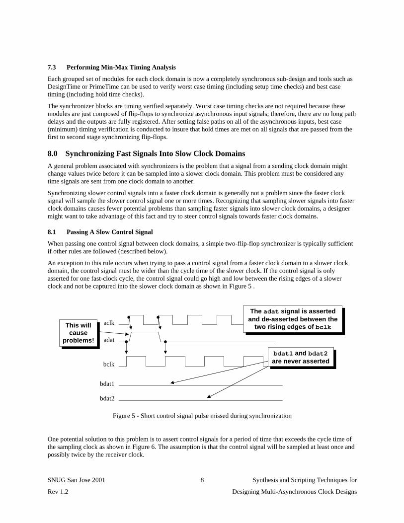
An exception to this rule occurs when trying to pass a control signal from a faster clock domain to a slower clockdomain, the control signal must be wider than the cycle time of the slower clock. If the control signal is onlyasserted for one fast-clock cycle, the control signal could go high and low between the rising edges of a slowerclock and not be captured into the slower clock domain as shown in Figure 5 .
adat
bdat1
bdat2
aclk
bclk
This willcause
problems!
The adat signal is assertedand de-asserted between the
two rising edges of bclk
bdat1 and bdat2are never asserted
Figure 5 - Short control signal pulse missed during synchronization
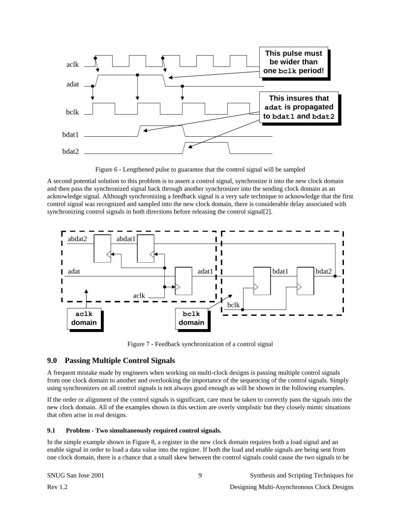
One potential solution to this problem is to assert control signals for a period of time that exceeds the cycle time ofthe sampling clock as shown in Figure 6. The assumption is that the control signal will be sampled at least once andpossibly twice by the receiver clock.
SNUG San Jose 2001 Synthesis and Scripting Techniques for
Rev 1.2 Designing Multi-Asynchronous Clock Designs
9
adat
bdat1
bdat2
aclk
bclk
This pulse mustbe wider than
one bclk period!
This insures thatadat is propagatedto bdat1 and bdat2
Figure 6 - Lengthened pulse to guarantee that the control signal will be sampled
A second potential solution to this problem is to assert a control signal, synchronize it into the new clock domainand then pass the synchronized signal back through another synchronizer into the sending clock domain as anacknowledge signal. Although synchronizing a feedback signal is a very safe technique to acknowledge that the firstcontrol signal was recognized and sampled into the new clock domain, there is considerable delay associated withsynchronizing control signals in both directions before releasing the control signal[2].
aclkbclk
adat adat1 bdat1 bdat2
abdat1abdat2
bclkdomain
aclkdomain
Figure 7 - Feedback synchronization of a control signal
9.0 Passing Multiple Control SignalsA frequent mistake made by engineers when working on multi-clock designs is passing multiple control signalsfrom one clock domain to another and overlooking the importance of the sequencing of the control signals. Simplyusing synchronizers on all control signals is not always good enough as will be shown in the following examples.
If the order or alignment of the control signals is significant, care must be taken to correctly pass the signals into thenew clock domain. All of the examples shown in this section are overly simplistic but they closely mimic situationsthat often arise in real designs.
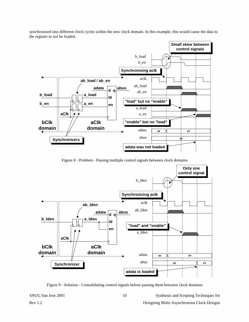
9.1 Problem - Two simultaneously required control signals.
In the simple example shown in Figure 8, a register in the new clock domain requires both a load signal and anenable signal in order to load a data value into the register. If both the load and enable signals are being sent fromone clock domain, there is a chance that a small skew between the control signals could cause the two signals to be
SNUG San Jose 2001 Synthesis and Scripting Techniques for
Rev 1.2 Designing Multi-Asynchronous Clock Designs
10
synchronized into different clock cycles within the new clock domain. In this example, this would cause the data tothe register to not be loaded.
b_load
aClk
bClkdomain
aClkdomain
a_load
ab_load / ab_en
b_en a_en
Synchronizers
abusadata
en
ld
d q
00
00 FF
b_load
ab_load
b_en
ab_en
a_loada_en
adata
abus
aclk
Small skew betweencontrol signals
"enable" but no "load"
"load" but no "enable"
adata was not loaded
Synchronizing aclk
Figure 8 - Problem - Passing multiple control signals between clock domains
FF
FF
b_lden
aClk
bClkdomain
aClkdomain
a_lden
ab_lden
Synchronizer
abusadata
en
ld
d q
00
00
b_lden
ab_lden
a_lden
adata
abus
aclk
"load" and "enable"
adata is loaded
Only onecontrol signal
Synchronizing aclk
Figure 9 - Solution - Consolidating control signals before passing them between clock domains
SNUG San Jose 2001 Synthesis and Scripting Techniques for
Rev 1.2 Designing Multi-Asynchronous Clock Designs
11
The solution to the problem in this simple example is easy. As shown in Figure 9, drive both the load and enableregister input signals in the new clock domain from just one control signal. This will remove the potential for thecontrol signals arriving shifted in time.
9.2 Problem - Two phase-shifted sequencing control signals.
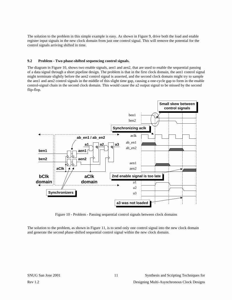
The diagram in Figure 10, shows two enable signals, aen1 and aen2, that are used to enable the sequential passingof a data signal through a short pipeline design. The problem is that in the first clock domain, the aen1 control signalmight terminate slightly before the aen2 control signal is asserted, and the second clock domain might try to samplethe aen1 and aen2 control signals in the middle of this slight time gap, causing a one-cycle gap to form in the enablecontrol-signal chain in the second clock domain. This would cause the a2 output signal to be missed by the secondflip-flop.
ben1
aClk
bClkdomain
aClkdomain
aen1
ab_en1 / ab_en2
ben2 aen2
a3q qa2a1
Synchronizers
ben1
ab_en1
ben2
ab_en2
aen1aen2
a1a2
aclk
a3
2nd enable signal is too late
a3 was not loaded
Small skew betweencontrol signals
Synchronizing aclk
Figure 10 - Problem - Passing sequential control signals between clock domains
The solution to the problem, as shown in Figure 11, is to send only one control signal into the new clock domainand generate the second phase-shifted sequential control signal within the new clock domain.
SNUG San Jose 2001 Synthesis and Scripting Techniques for
Rev 1.2 Designing Multi-Asynchronous Clock Designs
12
Synchronizers
ben1
aClk
bClkdomain
aClkdomain
aen1
ab_en
aen2
a3q qa2a1
a3 loaded
Synchronizing aclk
ben1
ab_en1
aen1aen2
a1a2
aclk
a3
Only onecontrol signal
Figure 11 - Solution - Logic to generate the proper sequencing signals in the new clock domains
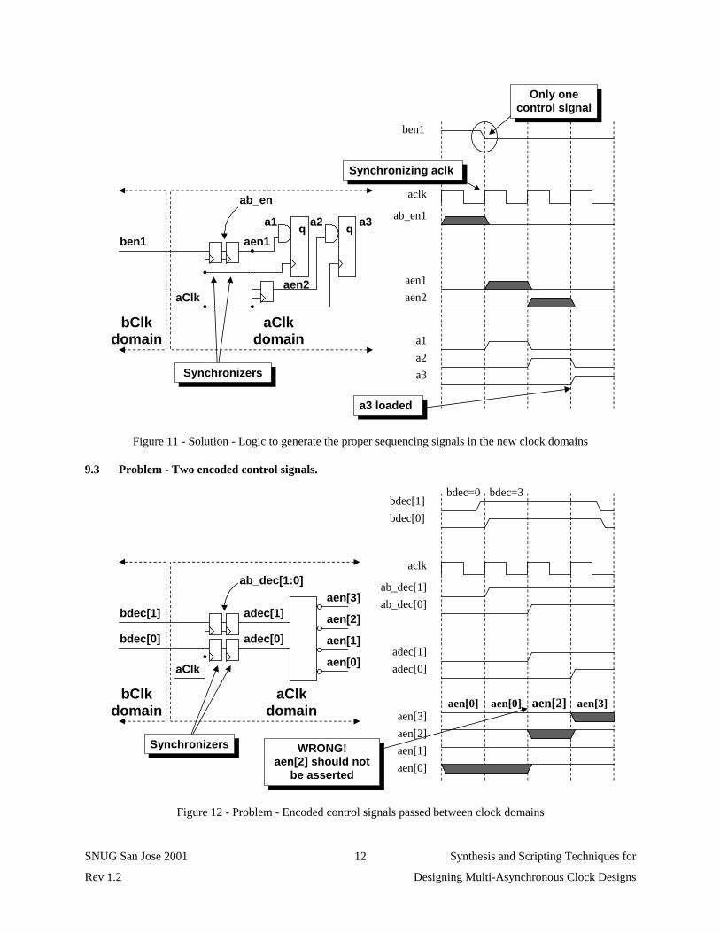
9.3 Problem - Two encoded control signals.
bdec[1]
aClk
bClkdomain
aClkdomain
adec[1]
ab_dec[1:0]aen[3]
aen[2]
aen[1]
aen[0]
bdec[0] adec[0]
Synchronizers WRONG!aen[2] should not
be asserted
bdec[1]
ab_dec[1]
bdec[0]
ab_dec[0]
adec[1]adec[0]
aen[3]aen[2]aen[1]aen[0]
aen[0] aen[0] aen[2] aen[3]
bdec=0 bdec=3
aclk
Figure 12 - Problem - Encoded control signals passed between clock domains
SNUG San Jose 2001 Synthesis and Scripting Techniques for
Rev 1.2 Designing Multi-Asynchronous Clock Designs
13
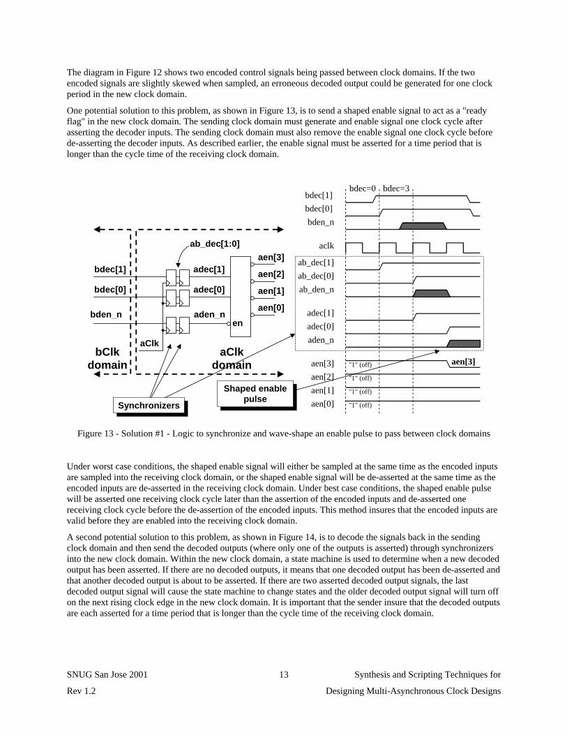
The diagram in Figure 12 shows two encoded control signals being passed between clock domains. If the twoencoded signals are slightly skewed when sampled, an erroneous decoded output could be generated for one clockperiod in the new clock domain.
One potential solution to this problem, as shown in Figure 13, is to send a shaped enable signal to act as a "readyflag" in the new clock domain. The sending clock domain must generate and enable signal one clock cycle afterasserting the decoder inputs. The sending clock domain must also remove the enable signal one clock cycle beforede-asserting the decoder inputs. As described earlier, the enable signal must be asserted for a time period that islonger than the cycle time of the receiving clock domain.
Shaped enablepulse
Synchronizers
en
bdec[1]
aClkbClk
domain
adec[1]
ab_dec[1:0]aen[3]
aen[2]
aen[1]
aen[0]
bdec[0] adec[0]
bden_n aden_n
aClkdomain
bdec[1]
bden_n
ab_dec[1]
bdec[0]
ab_dec[0]
adec[1]adec[0]
aen[3]aen[2]aen[1]aen[0]
bdec=0 bdec=3
aclk
ab_den_n
aden_n
aen[3]
"1" (off)
"1" (off)
"1" (off)
"1" (off)
Figure 13 - Solution #1 - Logic to synchronize and wave-shape an enable pulse to pass between clock domains
Under worst case conditions, the shaped enable signal will either be sampled at the same time as the encoded inputsare sampled into the receiving clock domain, or the shaped enable signal will be de-asserted at the same time as theencoded inputs are de-asserted in the receiving clock domain. Under best case conditions, the shaped enable pulsewill be asserted one receiving clock cycle later than the assertion of the encoded inputs and de-asserted onereceiving clock cycle before the de-assertion of the encoded inputs. This method insures that the encoded inputs arevalid before they are enabled into the receiving clock domain.
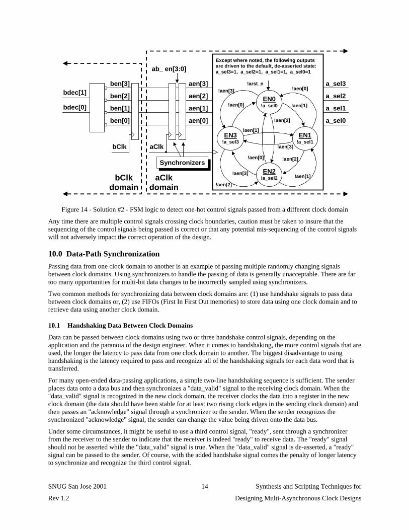
A second potential solution to this problem, as shown in Figure 14, is to decode the signals back in the sendingclock domain and then send the decoded outputs (where only one of the outputs is asserted) through synchronizersinto the new clock domain. Within the new clock domain, a state machine is used to determine when a new decodedoutput has been asserted. If there are no decoded outputs, it means that one decoded output has been de-asserted andthat another decoded output is about to be asserted. If there are two asserted decoded output signals, the lastdecoded output signal will cause the state machine to change states and the older decoded output signal will turn offon the next rising clock edge in the new clock domain. It is important that the sender insure that the decoded outputsare each asserted for a time period that is longer than the cycle time of the receiving clock domain.
SNUG San Jose 2001 Synthesis and Scripting Techniques for
Rev 1.2 Designing Multi-Asynchronous Clock Designs
14
!aen[2]Synchronizers
a_sel3
a_sel2
a_sel1
a_sel0
ben[3]
ben[2]
ben[1]
ben[0]
bdec[1]
bClk
bClkdomain
ab_ en[3:0]
bdec[0]
aClkdomain
aClk
aen[3]
aen[2]
aen[1]
aen[0]
!aen[2]
!aen[3]
!aen[1]
!aen[0]!arst_n
!aen[1]
!aen[1]
!aen[0]
!aen[0]
!aen[2]
!aen[3]
!aen[3]
EN0!a_sel0
EN1!a_sel1
EN2!a_sel2
EN3!a_sel3
Except where noted, the following outputsare driven to the default, de-asserted state:a_sel3=1, a_sel2=1, a_sel1=1, a_sel0=1
Figure 14 - Solution #2 - FSM logic to detect one-hot control signals passed from a different clock domain
Any time there are multiple control signals crossing clock boundaries, caution must be taken to insure that thesequencing of the control signals being passed is correct or that any potential mis-sequencing of the control signalswill not adversely impact the correct operation of the design.
10.0 Data-Path SynchronizationPassing data from one clock domain to another is an example of passing multiple randomly changing signalsbetween clock domains. Using synchronizers to handle the passing of data is generally unacceptable. There are fartoo many opportunities for multi-bit data changes to be incorrectly sampled using synchronizers.
Two common methods for synchronizing data between clock domains are: (1) use handshake signals to pass databetween clock domains or, (2) use FIFOs (First In First Out memories) to store data using one clock domain and toretrieve data using another clock domain.
10.1 Handshaking Data Between Clock Domains
Data can be passed between clock domains using two or three handshake control signals, depending on theapplication and the paranoia of the design engineer. When it comes to handshaking, the more control signals that areused, the longer the latency to pass data from one clock domain to another. The biggest disadvantage to usinghandshaking is the latency required to pass and recognize all of the handshaking signals for each data word that istransferred.
For many open-ended data-passing applications, a simple two-line handshaking sequence is sufficient. The senderplaces data onto a data bus and then synchronizes a "data_valid" signal to the receiving clock domain. When the"data_valid" signal is recognized in the new clock domain, the receiver clocks the data into a register in the newclock domain (the data should have been stable for at least two rising clock edges in the sending clock domain) andthen passes an "acknowledge" signal through a synchronizer to the sender. When the sender recognizes thesynchronized "acknowledge" signal, the sender can change the value being driven onto the data bus.
Under some circumstances, it might be useful to use a third control signal, "ready", sent through a synchronizerfrom the receiver to the sender to indicate that the receiver is indeed "ready" to receive data. The "ready" signalshould not be asserted while the "data_valid" signal is true. When the "data_valid" signal is de-asserted, a "ready"signal can be passed to the sender. Of course, with the added handshake signal comes the penalty of longer latencyto synchronize and recognize the third control signal.
SNUG San Jose 2001 Synthesis and Scripting Techniques for
Rev 1.2 Designing Multi-Asynchronous Clock Designs
15
10.2 Passing Data By FIFO Between Clock Domains
One of the most popular methods of passing data between clock domains is to use a FIFO. A dual port memory isused for the FIFO storage. One port is controlled by the sender which puts data into the memory as fast a one dataword (or one data bit for serial applications) per write clock. The other port is controlled by the receiver, whichpulls data out of memory one data word per read clock. Two control signals are used to indicate if the FIFO isempty, full or partially full. Two additional control signals are frequently used to indicate if the FIFO is almost fullor almost empty.
In theory, placing data into a shared memory with one clock and removing the data from the shared memory withanother clock seems like an easy and ideal solution to passing data between clock domains. For the most part it is,but generating accurate full and empty flags can be challenging.
10.3 FIFO Full & Empty
Determining that a FIFO is full or empty requires some type of mathematical manipulation and/or comparison ofwrite and read pointers. The problem is that the two pointers are generated in two different clock domains, so one orboth pointers must be synchronized into the opposite clock domain before mathematical and comparison operationscan be safely performed.
10.4 FIFO Pointers - Implemented as Binary Counters
Any FIFO pointer that must be synchronized into a different clock domain should not be implemented as a binarycounter.
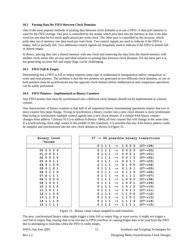
One characteristic of binary counters is that half of all sequential binary incrementing operations require that two ormore counter bits must change. Trying to synchronize a binary counter into a new clock domain is more problematicthan trying to synchronize multiple control signals into a new clock domain. If a simple 4-bit binary counterchanges from address 7 (binary 0111) to address 8 (binary 1000), all four counter bits will change at the same time.If a synchronizing clock edge comes in the middle of this transition, it is possible that any 4-bit binary pattern couldbe sampled and synchronized into the new clock domain as shown in Figure 15.
Binary CountValues
00 0 0 0 001 0 0 0 102 0 0 1 003 0 0 1 104 0 1 0 005 0 1 0 106 0 1 1 007 0 1 1 108 1 0 0 009 1 0 0 110 1 0 1 011 1 0 1 112 1 1 0 013 1 1 0 114 1 1 1 015 1 1 1 1
07 -> 08 possible binary transitions
0 1 1 1 -> 1 0 0 0 (07->08)0 1 1 1 -> 0 0 0 0 (07->00)0 1 1 1 -> 0 0 0 1 (07->01)0 1 1 1 -> 0 0 1 0 (07->02)0 1 1 1 -> 0 0 1 1 (07->03)0 1 1 1 -> 0 1 0 0 (07->04)0 1 1 1 -> 0 1 0 1 (07->05)0 1 1 1 -> 0 1 1 0 (07->06)0 1 1 1 -> 0 1 1 1 (07->07)0 1 1 1 -> 1 0 0 0 (07->08)0 1 1 1 -> 1 0 0 1 (07->09)0 1 1 1 -> 1 0 1 0 (07->10)0 1 1 1 -> 1 0 1 1 (07->11)0 1 1 1 -> 1 1 0 0 (07->12)0 1 1 1 -> 1 1 0 1 (07->13)0 1 1 1 -> 1 1 1 0 (07->14)0 1 1 1 -> 1 1 1 1 (07->15)
Figure 15 - Binary count values sampled in mid-transition
The new, synchronized binary value might trigger a false full or empty flag, or even worse, it might not trigger areal full or empty flag causing data to be lost due to FIFO overflow or causing bogus data to be read from the FIFOdue to attempting to read data when the FIFO is really empty.
SNUG San Jose 2001 Synthesis and Scripting Techniques for
Rev 1.2 Designing Multi-Asynchronous Clock Designs
16
10.5 FIFO Pointers - Implemented as Gray-Code Counters
Although binary counters work fine for addressing the memory, trying to synchronize binary counters into a newclock domain is problematic. A better approach for passing pointers between clock domains is to use a gray-codecounter for the two FIFO pointers. Gray code counters only change one bit at a time. If a synchronizing clock signalcomes in the middle of a gray code counter transition, the synchronized value will either be the old value or the newvalue because only one bit is changing at a time.
10.6 Designing Gray Code Counters
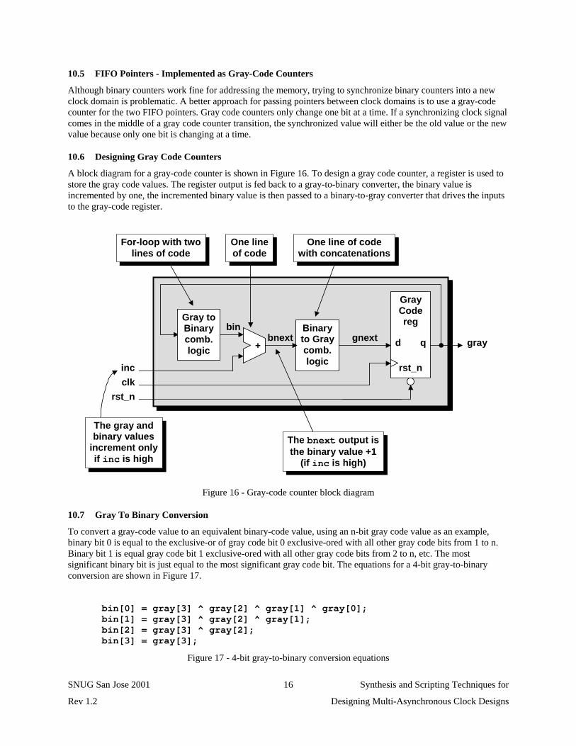
A block diagram for a gray-code counter is shown in Figure 16. To design a gray code counter, a register is used tostore the gray code values. The register output is fed back to a gray-to-binary converter, the binary value isincremented by one, the incremented binary value is then passed to a binary-to-gray converter that drives the inputsto the gray-code register.
Binaryto Graycomb.logic
GrayCodereg
The gray andbinary values
increment onlyif inc is high
The bnext output isthe binary value +1
(if inc is high)
inc
bingnext graybnext d
rst_n
q
rst_nclk
+
Gray toBinarycomb.logic
For-loop with twolines of code
One lineof code
One line of codewith concatenations
Figure 16 - Gray-code counter block diagram
10.7 Gray To Binary Conversion
To convert a gray-code value to an equivalent binary-code value, using an n-bit gray code value as an example,binary bit 0 is equal to the exclusive-or of gray code bit 0 exclusive-ored with all other gray code bits from 1 to n.Binary bit 1 is equal gray code bit 1 exclusive-ored with all other gray code bits from 2 to n, etc. The mostsignificant binary bit is just equal to the most significant gray code bit. The equations for a 4-bit gray-to-binaryconversion are shown in Figure 17.
bin[0] = gray[3] ^ gray[2] ^ gray[1] ^ gray[0];bin[1] = gray[3] ^ gray[2] ^ gray[1];bin[2] = gray[3] ^ gray[2];bin[3] = gray[3];
Figure 17 - 4-bit gray-to-binary conversion equations
SNUG San Jose 2001 Synthesis and Scripting Techniques for
Rev 1.2 Designing Multi-Asynchronous Clock Designs
17
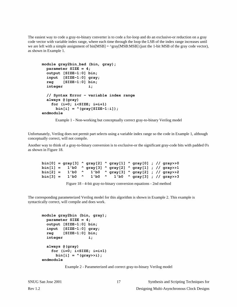
The easiest way to code a gray-to-binary converter is to code a for-loop and do an exclusive-or reduction on a graycode vector with variable index range, where each time through the loop the LSB of the index range increases untilwe are left with a simple assignment of bin[MSB] = ^gray[MSB:MSB] (just the 1-bit MSB of the gray code vector),as shown in Example 1.
module gray2bin_bad (bin, gray); parameter SIZE = 4; output [SIZE-1:0] bin; input [SIZE-1:0] gray; reg [SIZE-1:0] bin; integer i;
// Syntax Error - variable index range always @(gray) for (i=0; i<SIZE; i=i+1) bin[i] = ^(gray[SIZE-1:i]);endmodule
Example 1 - Non-working but conceptually correct gray-to-binary Verilog model
Unfortunately, Verilog does not permit part selects using a variable index range so the code in Example 1, althoughconceptually correct, will not compile.
Another way to think of a gray-to-binary conversion is to exclusive-or the significant gray-code bits with padded 0'sas shown in Figure 18.
bin[0] = gray[3] ^ gray[2] ^ gray[1] ^ gray[0] ; // gray>>0bin[1] = 1'b0 ^ gray[3] ^ gray[2] ^ gray[1] ; // gray>>1bin[2] = 1'b0 ^ 1'b0 ^ gray[3] ^ gray[2] ; // gray>>2bin[3] = 1'b0 ^ 1'b0 ^ 1'b0 ^ gray[3] ; // gray>>3
Figure 18 - 4-bit gray-to-binary conversion equations - 2nd method
The corresponding parameterized Verilog model for this algorithm is shown in Example 2. This example issyntactically correct, will compile and does work.
module gray2bin (bin, gray); parameter SIZE = 4; output [SIZE-1:0] bin; input [SIZE-1:0] gray; reg [SIZE-1:0] bin; integer i;
always @(gray) for (i=0; i<SIZE; i=i+1) bin[i] = ^(gray>>i);endmodule
Example 2 - Parameterized and correct gray-to-binary Verilog model
SNUG San Jose 2001 Synthesis and Scripting Techniques for
Rev 1.2 Designing Multi-Asynchronous Clock Designs
18
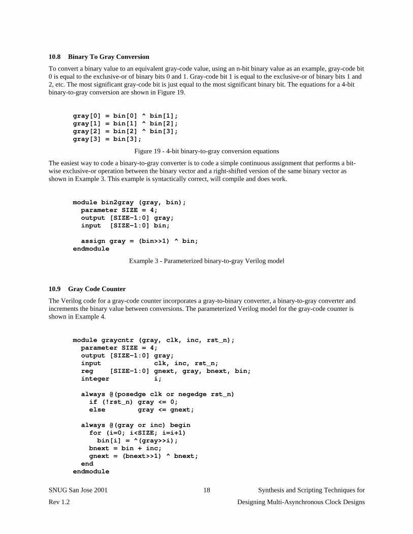
10.8 Binary To Gray Conversion
To convert a binary value to an equivalent gray-code value, using an n-bit binary value as an example, gray-code bit0 is equal to the exclusive-or of binary bits 0 and 1. Gray-code bit 1 is equal to the exclusive-or of binary bits 1 and2, etc. The most significant gray-code bit is just equal to the most significant binary bit. The equations for a 4-bitbinary-to-gray conversion are shown in Figure 19.
gray[0] = bin[0] ^ bin[1];gray[1] = bin[1] ^ bin[2];gray[2] = bin[2] ^ bin[3];gray[3] = bin[3];
Figure 19 - 4-bit binary-to-gray conversion equations
The easiest way to code a binary-to-gray converter is to code a simple continuous assignment that performs a bit-wise exclusive-or operation between the binary vector and a right-shifted version of the same binary vector asshown in Example 3. This example is syntactically correct, will compile and does work.
module bin2gray (gray, bin); parameter SIZE = 4; output [SIZE-1:0] gray; input [SIZE-1:0] bin;
assign gray = (bin>>1) ^ bin;endmodule
Example 3 - Parameterized binary-to-gray Verilog model
10.9 Gray Code Counter
The Verilog code for a gray-code counter incorporates a gray-to-binary converter, a binary-to-gray converter andincrements the binary value between conversions. The parameterized Verilog model for the gray-code counter isshown in Example 4.
module graycntr (gray, clk, inc, rst_n); parameter SIZE = 4; output [SIZE-1:0] gray; input clk, inc, rst_n; reg [SIZE-1:0] gnext, gray, bnext, bin; integer i;
always @(posedge clk or negedge rst_n) if (!rst_n) gray <= 0; else gray <= gnext;
always @(gray or inc) begin for (i=0; i<SIZE; i=i+1) bin[i] = ^(gray>>i); bnext = bin + inc; gnext = (bnext>>1) ^ bnext; endendmodule
SNUG San Jose 2001 Synthesis and Scripting Techniques for
Rev 1.2 Designing Multi-Asynchronous Clock Designs
19
Example 4 - Parameterized gray-code counter Verilog model
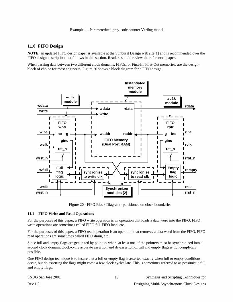
11.0 FIFO DesignNOTE: an updated FIFO design paper is available at the Sunburst Design web site[1] and is recommended over theFIFO design description that follows in this section. Readers should review the referenced paper.
When passing data between two different clock domains, FIFOs, or First-In, First-Out memories, are the design-block of choice for most engineers. Figure 20 shows a block diagram for a FIFO design.
wfull remptyEmptyflaglogic
Fullflaglogic
FIFO Memory(Dual Port RAM)
write
waddr
wdata
raddr
rdata
winc
wclk
wrst_n
FIFOwptr
rst_n
inc g
ginc
rinc
rclk
rrst_n
syncronizeto read clk
syncronizeto write clk
FIFOrptr
rst_n
incg
ginc
writewdata
wclkwrst_n
rclkrrst_n
rdata
rclkmodule
wclkmodule
Instantiatedmemorymodule
Synchronizermodules (2)
Figure 20 - FIFO Block Diagram - partitioned on clock boundaries
11.1 FIFO Write and Read Operations
For the purposes of this paper, a FIFO write operation is an operation that loads a data word into the FIFO. FIFOwrite operations are sometimes called FIFO fill, FIFO load, etc.
For the purposes of this paper, a FIFO read operation is an operation that removes a data word from the FIFO. FIFOread operations are sometimes called FIFO drain, etc.
Since full and empty flags are generated by pointers where at least one of the pointers must be synchronized into asecond clock domain, clock-cycle accurate assertion and de-assertion of full and empty flags is not completelypossible.
One FIFO design technique is to insure that a full or empty flag is asserted exactly when full or empty conditionsoccur, but de-asserting the flags might come a few clock cycles late. This is sometimes referred to as pessimistic fulland empty flags.
SNUG San Jose 2001 Synthesis and Scripting Techniques for
Rev 1.2 Designing Multi-Asynchronous Clock Designs
20
11.2 Pessimistic full and empty flags
A pessimistic full flag is a full signal that is asserted immediately when a FIFO becomes full but is de-asserted late(it is not de-asserted until a few read-clock cycles later).
Because the write pointer does not have to be synchronized before testing for a full condition, the full flag will beasserted immediately when the FIFO goes full. The FIFO might not actually be completely full because the readpointer might have incremented but the new read pointer value might not have been synchronized into the writeclock domain. Using the block diagram shown in Figure 20, the read pointer synchronized into the write clockdomain is always two write clocks behind the actual read pointer value, so the full flag might be asserted for twoextra write clocks. This typically is not a problem since the full flag is simply holding off transmission of more datafrom the data sending source for two extra write clock cycles. Pointers being synchronized into a new clock domainshould be gray code counters for reasons explained in sections 10.4 and section 10.5.
Similarly, because the read pointer does not have to be synchronized before testing for an empty condition, theempty flag will be asserted immediately when the FIFO goes empty. The FIFO might not actually be completelyempty because the write pointer might have incremented but the new write pointer value might not have beensynchronized into the read clock domain. Using the block diagram shown in Figure 20, the write pointersynchronized into the read clock domain is always two read clocks behind the actual write pointer value, so theempty flag might be asserted for two extra read clocks. This typically is not a problem since the empty flag ismerely informing the data receiver that data is not ready to be sent for another two read clock cycles. Again,pointers being synchronized into a new clock domain should be gray code counters for reasons explained in sections10.4 and section 10.5.
11.3 Full & Empty
A FIFO is full when both pointers are equal. A FIFO is also empty when both pointers are equal, so the FIFOpointers should be one bit larger than is necessary to address the full memory range. The extra bit is used as a flag tohelp determine if the FIFO is empty or full. If the extra, pointer MSBs are equal, it means that the FIFO pointershave wrapped back to address 0 an equal number of times and if the rest of the FIFO bits are equal, the FIFO isempty. If the extra, pointer MSBs are not equal, it means that the write pointer has wrapped back to address 0 onemore time than the read pointer and if the rest of the FIFO bits are equal, the FIFO is full.
12.0 Simulation IssuesAs mentioned in section 4.0, signals crossing clock boundaries through a synchronizer will experience setup andhold violations. That is why synchronizers are added to a design, to filter out the metastability effects of a signal thatchanges too close to the rising edge of a new clock domain clock signal.
When doing gate-level simulations on a multi-clock design, the ASIC library models of flip-flops are modeled withsetup and hold time expressions to match the timing specifications of the actual flip-flops. ASIC libraries typicallymodel flip-flops to drive X's (unknowns) on the flip-flop outputs when a timing violation occurs. When simulatinggate-level synchronizers, setup and hold time violations might cause ASIC libraries to issue setup and hold timeerror messages and the offending signals are frequently driven to an X value. These X-values propagate to the restof the design causing problems when trying to verify the functionality of the entire gate-level design.
Most Verilog simulators have a command option to ignore all timing checks, but this would also ignore the desiredtiming checks for the rest of the design.
It is possible to change the setup and hold time setting to zero for any ASIC library flip-flop that is used in asynchronizer, but that would cause all setup and hold time checks of all instances of that same type of flip-flop to beset to zero, including the flip-flops that you might want to use to test the rest of the design.
You could make copies of flip-flops from an ASIC library and store them into a new Verilog library with differentnames, set to zero all setup and hold times, then modify the design gate-level netlist, replacing all first stagesynchronizer ASIC library flip-flops with the modified library flip-flops without timing checks, but this could be anerror prone and tedious process that might have to be repeated each time a new netlist is generated or it might
SNUG San Jose 2001 Synthesis and Scripting Techniques for
Rev 1.2 Designing Multi-Asynchronous Clock Designs
21
require the creation of a makefile and scripts to automatically make the modifications each time a new netlist isgenerated.
A clever way to approach this problem suggested by Bhatnagar[3] is to use Synopsys commands to modify the SDFbackannotation of the setup and hold time on just the first stage flip-flop cells in the design. Bhatnagar points outthat the SDF file is instance based and therefore targeting the setup and hold times for the offending cells is moreeasily accomplished. Bhatnagar notes:
Instead of manually removing the setup and hold-time constructs from the SDF file, a better way is tozero out the setup and hold-times in the SDF file, only for the violating flops, i.e., replace the existingsetup and hold-time numbers with zero's.
Bhatnagar further points out that setup hold times of zero means that there can be no timing violation, therefore nounknowns propagated to the rest of the design. The following dc_shell command, given by Bhatnagar, is used tomake setup and hold times zero:
set_annotated_check 0 -setup -hold -from REG1/CLK -to REG1/D
Using a creative naming convention for the output of the first stage flip-flop of a synchronizer might make wild cardexpressions possible to easily backannotate all first stage flip-flop SDF setup and hold time values to zero usingvery few dc_shell commands.
13.0 ConclusionsCompletely synchronous one-clock design techniques are well known. Synthesis tools do their best work onsynchronous designs. Timing analysis tools are designed to report timing problems on one-clock synchronousdesigns. Synthesis scripts are easy to create for one-clock synchronous clock designs. The techniques in this paperare aimed at making the design look like multiple single clock designs!
• Partitioning non-synchronizer blocks so that there is only one clock per module permits easy verification ofcorrect timing by creating clock-domain sub-blocks that can be more easily verified with static timing analysistools.
• Partitioning synchronizer blocks to permit inputs from one and only one clock domain and clocking thesignals with only one asynchronous clock creates manageable synchronizer sub- blocks that can also be easilytimed.
• A clock-oriented naming convention can be useful to help identify signals that need to be timed within thedifferent asynchronous clock domains.
• Multiple control signals crossing clock domains require special attention to ensure that all control signals areproperly sequenced into a new clock domain.
The techniques described in this paper were developed to facilitate robust development and verification of multi-clock designs.
14.0 Errata and ChangesReaders are encouraged to send email to Cliff Cummings ( [email protected] ) any time they findpotential mistakes or if they would like to suggest improvements. Cliff is always interested in other techniques thatengineers are using.
14.1 Revision 1.2 (June 2005) - What Changed?
Errata - A colleague, Zenja Chao, pointed out that the equations of Figure 19 had the binary (bin) and gray(gray) labels swapped in the equations. The equations have been corrected.
SNUG San Jose 2001 Synthesis and Scripting Techniques for
Rev 1.2 Designing Multi-Asynchronous Clock Designs
22
References[1] Clifford E. Cummings, “Simulation and Synthesis Techniques for Asynchronous FIFO Design,” SNUG 2002 (Synopsys
Users Group Conference, San Jose, CA, 2002) User Papers, March 2002, Also available at:www.sunburst-design.com/papers
[2] ESNUG #281 - http://www.deepchip.com/posts/0281.html
[3] Himanshu Bhatnagar, Advanced ASIC Chip Synthesis, Kluwer Academic Publishers, 1999, pp. 202-203.
[4] Samir Palnitkar, Verilog HDL, A Guide to Digital Design and Synthesis, Sunsoft Press A Prentice Hall Title, 1996, pg. 193.
[5] Steve Golson, personal communication.
[6] William J. Dally and John W. Poulton, Digital Systems Engineering, Cambridge University Press, 1998, pg. 468.
[7] William J. Dally and John W. Poulton, Digital Systems Engineering, Cambridge University Press, 1998, pp. 462-513.
[8] William J. Dally and John W. Poulton, Digital Systems Engineering, Cambridge University Press, 1998, pp. 469-470.
Synopsys is a registered trademark of Synopsys, Inc.
Design Analyzer, DesignTime, PrimeTime and Synopsys Design Compiler are trademarks of Synopsys, Inc.
Author & Contact InformationCliff Cummings, President of Sunburst Design, Inc., is an independent EDA consultant and trainer with 23 years ofASIC, FPGA and system design experience and 13 years of Verilog, SystemVerilog, synthesis and methodologytraining experience.
Mr. Cummings, a member of the IEEE 1364 Verilog Standards Group (VSG) since 1994, is the only Verilog andSystemVerilog trainer to co-develop and co-author every IEEE 1364 Verilog Standard, the IEEE 1364.1 VerilogRTL Synthesis Standard, every Accellera SystemVerilog Standard, and the IEEE 1800 SystemVerilog Standard.
Mr. Cummings holds a BSEE from Brigham Young University and an MSEE from Oregon State University.
Sunburst Design, Inc. offers Verilog, Verilog Synthesis and SystemVerilog training courses. For more information,visit the www.sunburst-design.com web site.
Email address: [email protected]
An updated version of this paper can be downloaded from the web site: www.sunburst-design.com/papers
(Last updated June 20th, 2005)