2 marks - rajiv gandhi college of engineering and technology year/digital system design/unit...
TRANSCRIPT

CS T34-DIGITAL SYSTEM DESIGN Y2/S3
RAJIV GANDHI COLLEGE OF ENGINEERING & TECHNOLOGY Page 1 DEPARTMENT OF CSE
2 MARKS
1.Why J-K Flip Flop is called Master Flip Flop? (APRIL 2011)
Master-slave flip flop is designed using two separate flip flops. Out of these, one acts as
the master and the other as a slave. The figure of a master-slave J-K flip flop is shown below.
From the above figure you can see that both the J-K flip flops are presented in a series
connection. The output of the master J-K flip flop is fed to the input of the slave J-K flip flop.
The output of the slave J-K flip flop is given as a feedback to the input of the master J-K flip
flop. The clock pulse [Clk] is given to the master J-K flip flop and it is sent through a NOT Gate
and thus inverted before passing it to the slave J-K flip flop.
2.What is Shift Register? (NOV 2011)
A register capable of shifting the binary information held in each cell to its
neighboringcell, in a selected direction, is called a shift register. The logical configuration of a
shiftregister consists of a chain of flip‐flops in cascade, with the output of one flip ‐flop
connectedto the input of the next flip‐flop. All flip‐flops receive common clock pulses,which
activate the shift of data from one stage to the next.
3.Draw the logic diagram of SR flip-flop. (NOV 2012)
UNIT – III
Sequential Logic: Latches versus Flip Flops – SR, D, JK, Master Slave Flip Flops – Excitation table – Conversion of Flip flops – Counters: Asynchronous, synchronous, decade, presettable – Shift Registers: types, applications – Ring counter – Analysis and design of clocked sequential
circuits – Mealy and Moore models – State machine notations – state reduction techniques.

CS T34-DIGITAL SYSTEM DESIGN Y2/S3
RAJIV GANDHI COLLEGE OF ENGINEERING & TECHNOLOGY Page 2 DEPARTMENT OF CSE
4.Define Flip-Flop and write some common types of Flip-Flops. (APRIL/MAY 2012)
What is Flip-Flop? (APRIL 2013 - IT)
The memory elements used in clocked sequential circuits are called flip-flops. These
circuits are binary cells capable of storing one bit of information. Binary information can
enter a flip-flop in a variety of ways a few that gives rise to different types of flip-flops.
D flip flop
T flip flop
JK flip flop
SR flip flop
5.Explain Binary Ripple counters. (APRIL/MAY 2012)
A binary ripple counter consists of a series connection of complementing flip‐flops, with
the output of each flip‐flop connected to the C input of the next higher order flip‐flop. The
flip‐flop holding the least significant bit receives the incoming count pulses.
6.Define the term counter. (APRIL 2013)
A register that goes through a prescribed sequence of states upon the application of input
pulses is called a counter. The input pulses may be clock pulses, or they may originate from some external source and may occur at a fixed interval of time or at random. An n ‐bit binary
counter consists of n flip‐flops and can count in binary from 0 through 2n - 1. Counters are
available in two categories: ripple counters and synchronous counters. 7.What is Latches? (APRIL 2013 - IT)
A latch is an electronic logic circuit that has two inputs and one output. One of the inputs is called the SET input; the other is called the RESET input.
Latch circuits can be either active-high or active- low. The difference is determined by whether the operation of the latch circuit is triggered by HIGH or LOW signals on the inputs.
8.What is edge-triggered flip-flop? (APR'11)
`The problem of race around condition can solved by edge triggering flip flop. The term
edge triggering means that the flip-flop changes state either at the positive edge or negative edge
of the clock pulse and it is sensitive to its inputs only at this transition of the clock.
CS T34-DIGITAL SYSTEM DESIGN Y2/S3
RAJIV GANDHI COLLEGE OF ENGINEERING & TECHNOLOGY Page 3 DEPARTMENT OF CSE
The three basic types are introduced here: S-R, J-K and D.
9.What are hazards? (or) Define essential hazard. (NOV 2011) (APRIL/MAY 2014).
Hazards in any system are obviously an un-desirable effect caused by either a deficency in the
system or external.influences. In digital logic hazards are usually refered to in one of three ways: Static Hazards
Dynamic Hazards
Function Hazards These logic hazards are all subsets of the same problem: - When changes in the input variables
do not change the output due to some form of delay caused by logic elements (NOT, AND, OR gates etc), this results in the logic not performing its function properly.
10.What is register and state its usage. (NOV 2011)
A register is a group of flip‐flops, each one of which shares a common clock and is
capable of storing one bit of information. An n ‐bit register consists of a group of n flip‐flops
capable of storing n bits of binary information. In addition to the flip ‐flops, a register may have
combinational gates that perform certain data‐processing tasks. In its broadest definition, a
register consists of a group of flip‐flops together with gates that affect their operation.
11.What is synchronous counter?
In a synchronous counter, the clock pulse is applied simultaneously to all flip
flops. The output of the flip flop change state at the same instant. The speed of operation is high
compared to an asynchronous counter.
12.What is an excitation table?
During the design process we usually know the transition from present state to
next state and wish to find the flip flop input conditions that will cause the required transition. A
table which lists the required inputs for a given chance of state is called an excitation table.
13.Name the different types of counter.
Synchronous counter
Asynchronous counter
i) UP counter
ii) DOWN counter
iii) Modulo –N counter
iv) UP/DOWN counter
14.Define Blocking assignment statement. (APRIL 2013 - IT)

CS T34-DIGITAL SYSTEM DESIGN Y2/S3
RAJIV GANDHI COLLEGE OF ENGINEERING & TECHNOLOGY Page 4 DEPARTMENT OF CSE
Blocking assignment statements are executed sequentiallyin the order that they are listed
in a sequential block; when they execute, they have animmediate effect on the contents of
memory before the next statement can be executed. A general rule is to use blocking
assignments whensequential ordering is imperative and in cyclic behavior that is level
sensitive (i.e., incombinational logic).
15.What is asynchronous counter?
In an asynchronous counter, the clock pulse is applied to the first flip flops. The
change of state in the output of this flip flop serves as a clock pulse to the next flip flop and so
on. Here all the flip flops do not change state at the same instant and hence speed is less.
11 MARKS
1. Explain in detail about the SR latch/SR Flip. (11) (APR'13 - IT)
An SR latch is shown in figure 13.3. The latch Truth table is shown in the following table.
The two inputs, S and R denote ``set'' and ``reset'' respectively.
The latch has memory, and the present output is dependent on the state of the latch.
Thus the output at instant, denoted by Qn is dependent on output at (n-1)th instant, denoted
by Qn-1.
Figure 13.3: Construction of a latch from NOR gates
S R
1 0 1 0
0 1 0 1
1 1 0 0
0 0
Note that in state, Qn both and are 0, which seems absurd. Thus,
conventionally, the state is said to be ``not allowed''.

CS T34-DIGITAL SYSTEM DESIGN Y2/S3
RAJIV GANDHI COLLEGE OF ENGINEERING & TECHNOLOGY Page 5 DEPARTMENT OF CSE
A similar latch, known as latch is constructed using NAND gates (as opposed to
NOR gates for latch). The students should again check that the working of the latch
coheres with that of the truth table.
Figure 13.4: Construction of a latch from NAND gates
0 1 1 0
1 0 0 1
0 0 1 1
1 1
To avoid ``race'' between the inputs, to have a control on when the input affects the latch, the
circuit 13.5 is often implemented.
Fig. SR flip flop
Table(a): RS truth table
Table(b): RS Excitation table
The inputs have an effect on the latch only when , otherwise, the previous state is
maintained. The input may be a clock, so that whatever transitions in and take place
S R Qn+1
0 0 Qn
0 1 1
1 0 0
1 1 * Qn Qn+1 R S
0 0 X 0
0 1 0 1
1 0 1 0
1 1 0 X

CS T34-DIGITAL SYSTEM DESIGN Y2/S3
RAJIV GANDHI COLLEGE OF ENGINEERING & TECHNOLOGY Page 6 DEPARTMENT OF CSE
before the clock changes to do not affect the outputs, and only when the inputs have
become stable is the system affected.
2. Describe the design procedure of JK flip-flop.(5) (APR/MAY'12)
The circuit diagram and truth-table of a J-K flip flop is shown below.
The behavior of inputs J and K is same as the S and R inputs of the S-R flip flop.
The letter J stands for SET and the letter K stands for CLEAR.
When both the inputs J and K have a HIGH state, the flip-flop switch to the complement
state.
So, for a value of Q = 1, it switches to Q=0 and for a value of Q = 0, it switches to Q=1.

CS T34-DIGITAL SYSTEM DESIGN Y2/S3
RAJIV GANDHI COLLEGE OF ENGINEERING & TECHNOLOGY Page 7 DEPARTMENT OF CSE
The circuit includes two 3- input AND gates.
The output Q of the flip flop is returned back as a feedback to the input of the AND along
with other inputs like K and clock pulse [CP].
So, if the value of CP is ’1′, the flip flop gets a CLEAR signal and with the condition that
the value of Q was earlier 1.
Similarly output Q’ of the flip flop is given as a feedback to the input of the AND along
with other inputs like J and clock pulse [CP].
So the output becomes SET when the value of CP is 1 only if the value of Q’ was earlier
1.
The output may be repeated in transitions once they have been complimented for J=K=1
because of the feedback connection in the JK flip-flop.
This can be avoided by setting a time duration lesser than the propagation delay through
the flip-flop.
The restriction on the pulse width can be eliminated with a
master-slave or edge-triggered construction.
TRUTH TABLE EXCITATION TABLE
3. What is a Flip-Flop? Explain the working principle of D Flip-Flop, T Flip-Flop in
detail. (11) (APR'12)
D FLIP FLOP
The circuit diagram and truth table is given below.
J K Qn+1
0 0 Qn
0 1 0
1 0 1
1 1
Qn Qn+1 J J
0 0 0 X
0 1 1 X
1 0 X 1
1 1 X 0

CS T34-DIGITAL SYSTEM DESIGN Y2/S3
RAJIV GANDHI COLLEGE OF ENGINEERING & TECHNOLOGY Page 8 DEPARTMENT OF CSE
D flip flop is actually a slight modification of the above explained clocked SR flip-
flop.
From the figure you can see that the D input is connected to the S input and the
complement of the D input is connected to the R input.
The D input is passed on to the flip flop when the value of CP is ’1′.
When CP is HIGH, the flip flop moves to the SET state. If it is ’0′, the flip flop
switches to the CLEAR state.
T FLIP FLOP
This is a much simpler version of the J-K flip flop. Both the J and K inputs are
connected together and thus are also called a single input J-K flip flop.
When clock pulse is given to the flip flop, the output begins to toggle.
Here also the restriction on the pulse width can be eliminated with a master-slave
or edge-triggered construction.
Take a look at the circuit and truth table below.

CS T34-DIGITAL SYSTEM DESIGN Y2/S3
RAJIV GANDHI COLLEGE OF ENGINEERING & TECHNOLOGY Page 9 DEPARTMENT OF CSE
4. Explain in detail about analysis of clocked sequential circuits.
Analysis describes what a given circuit will do under certain operating conditions.
The behavior of a clocked sequential circuit is determined from the inputs, the outputs,
and the state of its flip-flops.
The outputs and the next state are both a function of the inputs and the present state.
The analysis of a sequential circuit consists of obtaining a table or a diagram for the time
sequence of inputs, outputs, and internal states.
It is also possible to write Boolean expressions that describe the behavior of the
sequential circuit. These expressions must include the necessary time sequence, either
directly or indirectly.
A state table and state diagram are then presented to describe the behavior of the
sequential circuit.

CS T34-DIGITAL SYSTEM DESIGN Y2/S3
RAJIV GANDHI COLLEGE OF ENGINEERING & TECHNOLOGY Page 10 DEPARTMENT OF CSE
The procedure for analysis of synchronous sequential circuits can be summarized by a list
of recommended steps:
1. From the given logic diagram, obtain the state equation.
2. From the state equation, generate the state table.
3. Draw the state diagram using state table.
4. The steps presented in this example are summarized below:
Circuit diagram- State Equations – State table - State diagram
State equation
The behavior of a clocked sequential circuit can be described algebraically by means of state equations.
A state equation (also called a transition equation ) specifies the next state as a function
of the present state and inputs.
State Table
The time sequence of inputs, outputs, and flip-flop states can be enumerated in a state
table (sometimes called a transition table ).
The table consists of four sections labeled present state, input, next state, and output .
The present-state section shows the states of flip-flops A and B at any given time t .
The input section gives a value of x for each possible present state.
The next-state section shows the states of the flip-flops one clock cycle later, at time
t + 1.
The output section gives the value of y at time t for each present state and input condition.
State Diagram
The information available in a state table can be represented graphically in the form of a
state diagram.
In this type of diagram, a state is represented by a circle, and the (clock-triggered)
transitions between states are indicated by directed lines connecting the circles.
The binary number inside each circle identifies the state of the flip-flops.
The directed lines are labeled with two binary numbers separated by a slash.
The input value during the present state is labeled first, and the number after the slash
gives the output during the present state with the given input.
For example, the directed line from state 00 to 01 is labeled 1/0, meaning that when the
sequential circuit is in the present state 00 and the input is1, the output is 0.
After the next clock cycle, the circuit goes to the next state, 01.

CS T34-DIGITAL SYSTEM DESIGN Y2/S3
RAJIV GANDHI COLLEGE OF ENGINEERING & TECHNOLOGY Page 11 DEPARTMENT OF CSE
5. A sequential circuit has two D flip-flop, one inputs x, and one output y. Derive the state table and state diagram of the sequential circuit.
SOLUTION:
1. State equation
A(t+1)=Ax+Bx
B(t+1)=Ax’
Y=Ax’+Bx’
2. State table
3. State diagram

CS T34-DIGITAL SYSTEM DESIGN Y2/S3
RAJIV GANDHI COLLEGE OF ENGINEERING & TECHNOLOGY Page 12 DEPARTMENT OF CSE
6. Construct a JK flip-flop using a D flip- flop, a 4-to-1-line multiplexer and an inverter.
Solution:
Q
QSET
CLR
DS1
S4
D
C2C1 ENB
Multiplexer
0
1
KJ
clk
7. A sequential circuit has one flip-flop Q, two inputs x and y, and one output S. It consists
of a full-adder circuit connected to a D flip-flop, as shown. Derive the state table and state diagram of the sequential circuit.
Solution:
1. FA equations: QYXS
FA
Q
QSET
CLR
D
X
YS
C
CLK
FA
Q
QSET
CLR
D
X
YS
C
CLK

CS T34-DIGITAL SYSTEM DESIGN Y2/S3
RAJIV GANDHI COLLEGE OF ENGINEERING & TECHNOLOGY Page 13 DEPARTMENT OF CSE
C = XY + XQ + YQ
2. Input equation:
DQ = C = XY + XQ + YQ (from the FA equations or from the K-map)
3. Characteristic equation:
Q(t+1) = D = XY + XQ + YQ
4. State equation:
Q(t+1) = C
5. State Table:
PRESENT
STATE INPUTS
NEXT
STATE OUTPUT
Q X Y Q S
0 0 0 0 0
0 0 1 0 1
0 1 0 0 1
0 1 1 1 0
1 0 0 0 1
1 0 1 1 0
1 1 0 1 0
1 1 1 1 1
State Diagram:
8. A sequential circuit has two JK flip-flops A and B and one input x. The circuit is described by the following flip-flop input equations :
JA = x KA = B' JB = x KB = A
0 1
11/0
00/1
01/010/011/1
10/100/001/1
0 1
11/0
00/1
01/010/011/1
10/100/001/1

CS T34-DIGITAL SYSTEM DESIGN Y2/S3
RAJIV GANDHI COLLEGE OF ENGINEERING & TECHNOLOGY Page 14 DEPARTMENT OF CSE
(a) Derive the state equation A(t+1) and B(t+1) by substituting the input equations for the J and K variables.
(b) Draw the state diagram of the circuit.
Solution:
1. State equation:
Q(t+1) = JQ' + K'Q
2. Characteristic equation:
A (t+1) = XA' + BA
B (t+1) = XB' + A'B 3. State Table:
PRESENT
STATE INPUT NEXT STATE FLIP-FLOP INPUTS
A B X A B JA KA JB KB
0 0 0 0 0 0 1 0 0
0 0 1 1 1 1 1 1 0
0 1 0 0 1 0 0 0 0
0 1 1 1 1 1 0 1 0
1 0 0 0 0 0 1 0 1
1 0 1 0 1 1 1 1 1
1 1 0 1 0 0 0 0 1
1 1 1 1 0 1 0 1 1
4. State Diagram:
9. Explain in detail about design of clocked sequential circuits.
00 11
01 10
0
0 1
1
1
0
00 11
01 10
0
0 1
1
1
0
0, 1

CS T34-DIGITAL SYSTEM DESIGN Y2/S3
RAJIV GANDHI COLLEGE OF ENGINEERING & TECHNOLOGY Page 15 DEPARTMENT OF CSE
The procedure for designing synchronous sequential circuits can be summarized by a list of
recommended steps:
1. From the word description and specifications of the desired operation, derive a state
diagram for the circuit.
2. Reduce the number of states if necessary.
3. Assign binary values to the states.
4. Obtain the binary-coded state table.
5. Choose the type of flip-flops to be used.
6. Derive the simplified flip- flop input equations and output equations.
7. Draw the logic diagram.
10. Reduce the number of states in the following table and tabulate the reduced state table.
PRESENT
STATE
NEXT STATE OUTPUT
X=0 X=1 X=0 X=1
a f b 0 0
b d c 0 0
c f e 0 0
d g a 1 0
e d c 0 0
f f b 1 1
g g h 0 1
h g a 1 0
Solution:
States b,e are the same ,we will replace state e with state b . States d,h are the same ,we will replace state h with state d .
PRESENT
STATE
NEXT STATE OUTPUT
X=0 X=1 X=0 X=1
a f b 0 0
b d c 0 0
c f b 0 0
d g a 1 0
f f b 1 1
g g d 0 1
States a,c are the same ,we will replace state c with state a .
PRESENT NEXT STATE OUTPUT

CS T34-DIGITAL SYSTEM DESIGN Y2/S3
RAJIV GANDHI COLLEGE OF ENGINEERING & TECHNOLOGY Page 16 DEPARTMENT OF CSE
STATE X=0 X=1 X=0 X=1
a f b 0 0
b d a 0 0
d g a 1 0
f f b 1 1
g g d 0 1
11. Starting from state a, and the input sequence 01110010011,determine the output sequence for:
(a) the state table of the previous problem and (b) the reduced state table from the previous problem. Show that the same output sequence
is obtained for both.
Solution:
(a) using the state table
state a f b c e d g h g g h a
input 0 1 1 1 0 0 1 0 0 1 1
output 0 1 0 0 0 1 1 1 0 1 0
(b) Using the reduced state table
state a f b a b d g d g g d a
input 0 1 1 1 0 0 1 0 0 1 1
output 0 1 0 0 0 1 1 1 0 1 0
The same output sequence is obtained for both.
12. Design a sequential circuit with two D flip-flops A and B, and one input x. When x=0,
the state of the circuit remains the same. When x=1, the circuit goes through the state transitions from 00 to 01 to 11 to 10 back to 00, and repeats.
Solution:
1. State Diagram:
2. State Table:
PRESENT
STATE INPUT NEXT STATE
00 01
11 10
0
11
1
1
0
0
0
00 01
11 10
0
11
1
1
0
0
0

CS T34-DIGITAL SYSTEM DESIGN Y2/S3
RAJIV GANDHI COLLEGE OF ENGINEERING & TECHNOLOGY Page 17 DEPARTMENT OF CSE
A B X A B
0 0 0 0 0
0 0 1 0 1
0 1 0 0 1
0 1 1 1 1
1 0 0 1 0
1 0 1 0 0
1 1 0 1 1
1 1 1 1 0
3. Characteristic equation:
Q(t+1) = D
4. Input equations or State equations :
A(t+1) = DA (A,B,X) = ∑ (3,4,6,7) B(t+1) = DB (A,B,X) = ∑ (1,2,3,6)
K-maps :
DA
DA = BX + AX'
DB
DB = A'X + BX'
Circuit Diagram :
1111
10
10110100A
BX
1111
10
10110100A
BX
11
1110
101110A
BX
11
1110
101110A
BX

CS T34-DIGITAL SYSTEM DESIGN Y2/S3
RAJIV GANDHI COLLEGE OF ENGINEERING & TECHNOLOGY Page 18 DEPARTMENT OF CSE
13. Design a sequential circuit with two JK flip-flops A and B and two inputs E and x. If E =0 ,the circuit remains in the same state regardless of the value of x. When E =1 and x=1, the circuit goes through the state transitions from 00 to 01 to 10 to 11 back to 00,and
repeats. When E =1 and x=0, the circuit goes through the state transitions from 00 to 11 to 10 to 01 back to 00,and repeats.
Solution:
1. State Diagram:
2. State Table:
PRESENT
STATE INPUT NEXT STATE FLIP-FLOP INPUTS
A B E X A B JA KA JB KB
0 0 0 0 0 0 0 X 0 X
0 0 0 1 0 0 0 X 0 X
0 0 1 0 1 1 1 X 1 X
0 0 1 1 0 1 0 X 1 X
0 1 0 0 0 1 0 X X 0
0 1 0 1 0 1 0 X X 0
0 1 1 0 0 0 0 X X 1
Q
QSET
CLR
D
Q
QSET
CLR
D
CLK
A
B
X
00 01
11 10
00,01
11
11
00,01
00,01
00,01
1111
10
10
1010

CS T34-DIGITAL SYSTEM DESIGN Y2/S3
RAJIV GANDHI COLLEGE OF ENGINEERING & TECHNOLOGY Page 19 DEPARTMENT OF CSE
0 1 1 1 1 0 1 X X 1
1 0 0 0 1 0 X 0 0 X
1 0 0 1 1 0 X 0 0 X
1 0 1 0 0 1 X 1 1 X
1 0 1 1 1 1 X 0 1 X
1 1 0 0 1 1 X 0 X 0
1 1 0 1 1 1 X 0 X 0
1 1 1 0 1 0 X 0 X 1
1 1 1 1 0 0 X 1 X 1
K-maps :
JA
JA = BEX +B'EX' = E (BX)'
KA
KA = BEX +B'EX' = E (BX)'
JB
JB = E
KB
XXXX10
XXXX11
01001
10000
10110100AB
EX
XXXX10
XXXX11
01001
10000
10110100AB
EX
100010
010011
XXXX1
XXXX0
101110AB
EX
100010
010011
XXXX1
XXXX0
101110AB
EX
110010
XXXX11
XXXX1
11000
101110AB
EX
110010
XXXX11
XXXX1
11000
101110AB
EX
XXXX10
110011
11001
XXXX0
101110AB
EX
XXXX10
110011
11001
XXXX0
101110AB
EX

CS T34-DIGITAL SYSTEM DESIGN Y2/S3
RAJIV GANDHI COLLEGE OF ENGINEERING & TECHNOLOGY Page 20 DEPARTMENT OF CSE
KB = E
Circuit Diagram :
This sequential circuit behaves like a 2-bit up-down-counter, with E the enable of the whole
counter, and resets when it finishes counting, when X=1, it behaves like an up-counter, when
X=0, it behaves like a down-counter
Counters come in two categories: ripple counters and synchronous counters.
In a ripple counter, the flip-flop output transition serves as a source for triggering other
flip-flops. In other words, the CP inputs of all flip- flops (except the first) are triggered
not by the incoming pulses, but rather by the transition that occurs in other flip-flops.
In a synchronous counter, the input pulses are applied to all CP inputs of all flip- flops.
The change of state of a particular flip- flop is dependent on the present state of other flip-
flops.
Some common MSI ripple counters are Binary Ripple Counter and BCD Ripple
Counter.
1. Binary Ripple Counter
A binary ripple counter consists of a series connection of complementing flip-flops (T or
JK type), with the output of each flip- flop connected to the CP input of the next higher-
order flip-flop.
The flip-flop holding the least significant bit receives the incoming count pulses.
The small circle in the CP input indicates that theflip-flop complements during a
negative-going transition or when the output to which it is connected goes from 1 to 0.
J
Q
Q
K
SET
CLR
J
Q
Q
K
SET
CLR
A
B
A
B
E
CLK
14. Describe in detail about ripple counter/asynchronous counter?
CS T34-DIGITAL SYSTEM DESIGN Y2/S3
RAJIV GANDHI COLLEGE OF ENGINEERING & TECHNOLOGY Page 21 DEPARTMENT OF CSE
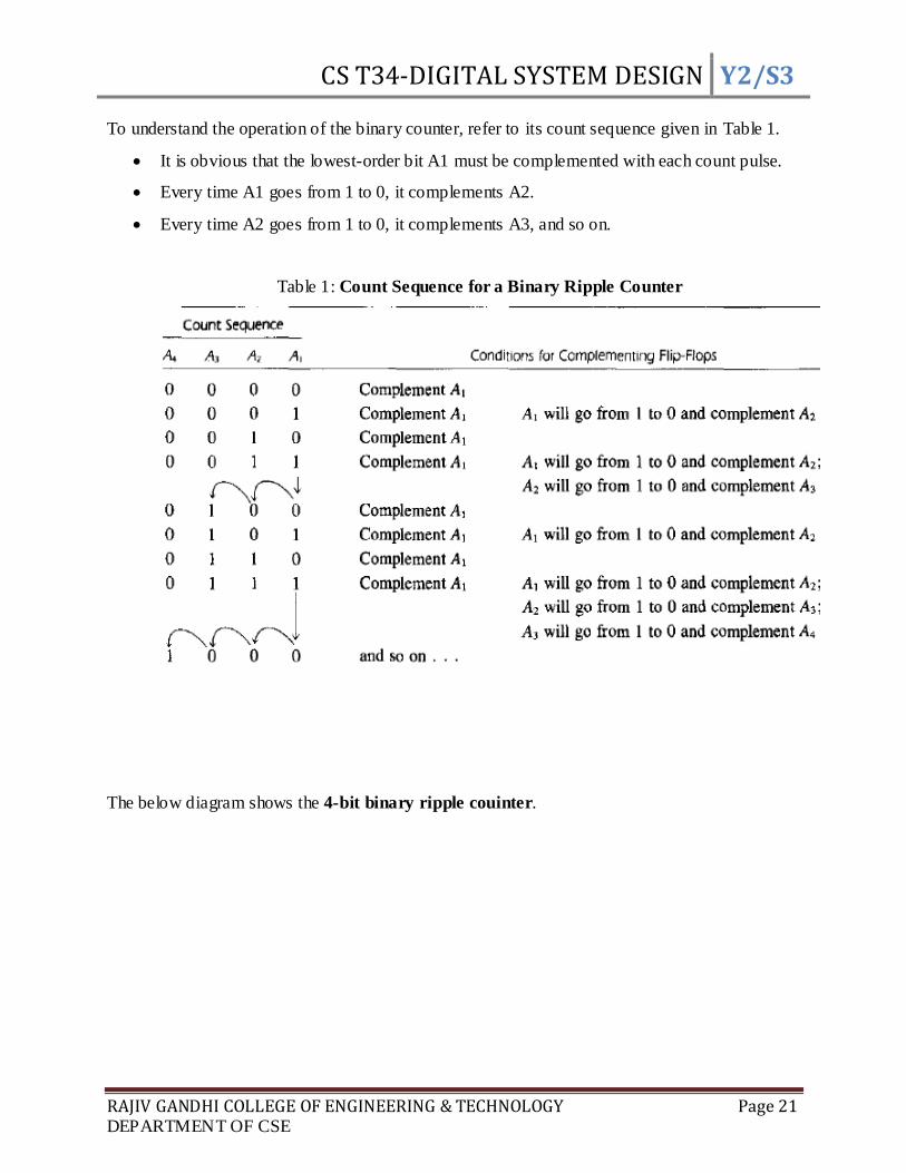
To understand the operation of the binary counter, refer to its count sequence given in Table 1.
It is obvious that the lowest-order bit A1 must be complemented with each count pulse.
Every time A1 goes from 1 to 0, it complements A2.
Every time A2 goes from 1 to 0, it complements A3, and so on.
Table 1: Count Sequence for a Binary Ripple Counter
The below diagram shows the 4-bit binary ripple couinter.

CS T34-DIGITAL SYSTEM DESIGN Y2/S3
RAJIV GANDHI COLLEGE OF ENGINEERING & TECHNOLOGY Page 22 DEPARTMENT OF CSE
2. BCD Ripple Counter
A decimal counter follows a sequence of ten states and returns to 0 after the count of 9.
Such a counter must have at least four flip-flops to represent each decimal digit, since a decimal
digit is represented by a binary code with at least four bits. The sequence of states in a decimal
counter is dictated by the binary code used to represent a decimal digit. If BCD is used, the
sequence of states is as shown in the state diagram of Fig. 2.
Signals that affect the flip-flop transition depend on the order in which they change from
1 to 0. Theoperation of the counter can be explained by a list of conditions for flip- flop
transitions. These conditions are derived from the logic diagram and from knowledge of how a
JK flip-flop operates. Remember that when the CP input goes from I to 0, the flip-flop is set if J
= I, is cleared if K = I, is complemented if J = K = I, and is left unchanged if J = K = 0. The
following are the conditions for each flip-flop state transition:

CS T34-DIGITAL SYSTEM DESIGN Y2/S3
RAJIV GANDHI COLLEGE OF ENGINEERING & TECHNOLOGY Page 23 DEPARTMENT OF CSE
1.Q1is complemented on the negative edge of every count pulse.
2, Q2is complemented if Q8= 0 and Q1goes from I to o. Q2is cleared if Q8 =and Q1
goes from 1 to 0.
3. Q4is complemented when Q2goes from I to o.
4. Q8is complemented when Q4 Q2 = 11 and Q, goes from I to o. Q8 is cleared ifeither
Q4 or Q2is 0 and Q1goes from 1 to 0.
Figure: BCD ripple counter
Synchronous counters are distinguished from ripple counters in that clock pulses are
applied to the CP inputs of all flip-flops. The common pulse triggers all the flip- flops
15. Describe in detail about synchronous counter?

CS T34-DIGITAL SYSTEM DESIGN Y2/S3
RAJIV GANDHI COLLEGE OF ENGINEERING & TECHNOLOGY Page 24 DEPARTMENT OF CSE
simultaneously, rather than one at a time in succession as in a ripple counter. If J = K = 0, the
flip- flop remains unchanged. If J = K = I, the flip-flop complements.
1. Synchronous binary counter
In a synchronous binary counter, the flip-flop in the lowest-order position is
complemented with every pulse. This means that itsJ and K inputs must be maintained at logic-1.
A flip-flop in any other position iscomplemented with a pulse provided all the bits in the lower-
order positions are equal to I, because the lower-order bits (when all I's) will change to D's on the
next count pulse. The binary count dictates that the next higher-order bit be complemented.
For example, if the present state of a 4-bit counter is A4A3A2A1= 0011, the next count
will be 0100. A1 is always complemented. A2 is complemented because the present state of AI =
I. A3 is complemented because the present state of A2A1 = 11. But A4 is not complemented
because the present state of A3A2A1 = 011, which does not give an all-1's condition.
Figure: synchronous binary counter
2. Binary Up-Down Counter

CS T34-DIGITAL SYSTEM DESIGN Y2/S3
RAJIV GANDHI COLLEGE OF ENGINEERING & TECHNOLOGY Page 25 DEPARTMENT OF CSE
A count-down binary counter can be constructed as shown in Fig. , except that the inputs
to the AND gates must come from the complement outputs Q' and not from the normal outputs Q
of the previous flip-flops. The two operations can be combined in one circuit.
When the up input control is 1, the circuit counts up, since the T inputs receive their
signals from the values of the previous normal outputs of the flip-flops.
When the down input control is I and the up input is 0, the circuit counts down,
since the complemented outputs of the previous flip-flops are applied to the T
inputs.
When the up and down inputs are both 0, the circuit does not change state but
remains in the same count.
When the up and down inputs are both 1, the circuit counts up. This ensures that
only one operation is performed at any given time.
Figure: binary up-down counter
16. Elaborate decade counter.

CS T34-DIGITAL SYSTEM DESIGN Y2/S3
RAJIV GANDHI COLLEGE OF ENGINEERING & TECHNOLOGY Page 26 DEPARTMENT OF CSE
To verify that these conditions result in the sequence required by a BCD ripple counter, it is
necessary to verify that the flip‐flop transitions indeed follow a sequence of states as specified by
the state diagram.
Q1 changes state after each clock pulse.
Q2 complements every time Q1 goes from 1 to 0, as long as Q8 = 0.
When Q8 becomes 1, Q2 remains at 0.
Q4 complements every time Q2 goes from 1 to 0.
Q8 remains at 0 as long as Q2 or Q4 is 0.
When both Q2 and Q4 become 1, Q8 complements when Q1 goes from 1 to 0.
Q8 is cleared on the next transition of Q1.
The BCD counter of Fig. 1 is a decade counter, since it counts from 0 to 9.
Figure.1:BCD counter
To count in decimal from 0 to 99, we need a two‐decade counter.
To count from 0 to 999, we need a three‐decade counter.
Multiple decade counters can be constructed by connecting BCD counters in cascade, one
for each decade.
A three‐decade counter is shown in Fig.2 .
The inputs to the second and third decades come from Q8 of the previous decade.

CS T34-DIGITAL SYSTEM DESIGN Y2/S3
RAJIV GANDHI COLLEGE OF ENGINEERING & TECHNOLOGY Page 27 DEPARTMENT OF CSE
When Q8 in one decade goes from 1 to 0, it triggers the count for the next higher order
decade while its own decade goes from 9 to 0.
Figure 2: three decade decimal BCD counter
Ring counter
A ring counter is a circular shift register with only one flip-flop being set at any
particular time; all others arecleared. The single bit is shifted from one flip-flop to the other to produce the sequence of timing signals. The below figure shows a 4-bit shift register connected
as a ring counter. The initial value of the register is 1000, which produces the variable T0. The single bit is shifted right with every clock pulse and circulates back from T3to T0.
17. Explain Johnson counter and ring counter.

CS T34-DIGITAL SYSTEM DESIGN Y2/S3
RAJIV GANDHI COLLEGE OF ENGINEERING & TECHNOLOGY Page 28 DEPARTMENT OF CSE
Johnson counter
A k-bit ring counter circulates a single bit among the flip-flops to provide k distinguishablestates.
The number of states can be doubled if the shift register is connected as a switch-tail ring counter.
A switch-tail ring counter is a circular shift register with the complement output of the last flip- flop connected to the input of the first flip- flop.
In general, a k-bit switch-tail ring counter will go through a sequence of 2k states.
Starting from all 0's, each shift operation inserts 1's from the le ft until the register is filled
with all 1's.
In the following sequences, 0's are inserted from the left until the register is again filled
with all 0's.

CS T34-DIGITAL SYSTEM DESIGN Y2/S3
RAJIV GANDHI COLLEGE OF ENGINEERING & TECHNOLOGY Page 29 DEPARTMENT OF CSE
18. What is register? Explain the types of shift register.
Register
Register is a group of flip flops for storing binary information.
Shift register
A register capable of shifting its binary information either to the right or to the left is
called a shift register.
Types of shift register
1. Serial in serial out shift register 2. Serial in parallel out 3. Parallel in serial out
4. Parallel in parallel out
Serial in serial out shift register
Serial in Parallel out shift register
parallel in parallel out shift register

CS T34-DIGITAL SYSTEM DESIGN Y2/S3
RAJIV GANDHI COLLEGE OF ENGINEERING & TECHNOLOGY Page 30 DEPARTMENT OF CSE
:Universal shift register
Shift registers provide the necessary input and output terminals for parallel transfer. They may also have both shift‐right and shift‐left capabilities. The most general shift register has the
following capabilities
Functions of Universal Shift Register
1. A clear control to clear the register to O.
2. A CP input for clock pulses to synchronize all operations.
3. A shift-right control to enable the shift-right operation and the serial input andoutput
lines associated with the shift right.
4. A shift-left control to enable the shift- left operation and the serial input and outputlines
associated with the shift left.
5. A parallel-load control to enable a parallel transfer and the n input lines associatedwith
the parallel transfern parallel output lines.
7. A control state that leaves the information in the register unchanged even thoughclock
pulses are continuously applied.
Figure: Four-bit universal shift register

CS T34-DIGITAL SYSTEM DESIGN Y2/S3
RAJIV GANDHI COLLEGE OF ENGINEERING & TECHNOLOGY Page 31 DEPARTMENT OF CSE
The circuit consists of four D flip‐flops and four multiplexers.
The four multiplexers have two common selection inputs s1 and s0.
Input 0 in each multiplexer is selected when s1s0 = 00, input 1 is selected when s1s0 =
01, and similarly for the other two inputs. The selection inputs control the mode of
operation of the register according to the function entries in Table.
When s1s0 = 00, the present value of the register is applied to the D inputs of the
flip‐flops.
This condition forms a path from the output of each flip ‐flop into the input of the same
flip‐flop, so that the output recirculates to the input in this mode of operation.
The next clock edge transfers into each flip‐flop the binary value it held previously, and
no change of state occurs.
When s1s0 = 01, terminal 1 of the multiplexer inputs has a path to the D inputs of the
flip‐flops. This causes a shift‐right operation, with the serial input transferred into
flip‐flop A3.
When s1s0 = 10, a shift‐left operation results, with the other serial input going into
flip‐flop A0. Finally, when s1s0 = 11, the binary information on the parallel input lines is
transferred into the register simultaneously during the next clock edge.
Note that data enters MSB_in for a shift‐right operation and enters LSB_in for a shift‐left
operation.
Clear_b is an active‐low signal that clears all of the flip‐flops.
19. Explain in detail about Serial Addition using shift register.
The serial transfer of information from register A to register B is done with shift registers,
as shown in the block diagram of Figure.

CS T34-DIGITAL SYSTEM DESIGN Y2/S3
RAJIV GANDHI COLLEGE OF ENGINEERING & TECHNOLOGY Page 32 DEPARTMENT OF CSE
The serial output ( SO ) of register A is connected to the serial input ( SI ) of register B.
To prevent the loss of information stored in the source register, the information in register
A is made to circulate by connecting the serial output to its serial input.
The two binary numbers to be added serially are stored in two shift registers.
The operation of the serial adder is as follows: Initially, register A holds the augend,
register B holds the addend, and the carry flip‐flop is cleared to 0.
The outputs ( SO ) of A and B provide a pair of significant bits for the full adder at x and
y.
Output Q of the flip‐flop provides the input carry at z.
Initially, register A and the carry flip‐flop are cleared to 0, and then the first number is
added from B. While B is shifted through the full adder, a second number is transferred to
it through its serial input.
The second number is then added to the contents of register A , while a third number is
transferred serially into register B.
This can be repeated to perform the addition of two, three, or more four‐bit numbers and
accumulate their sum in register A.

CS T34-DIGITAL SYSTEM DESIGN Y2/S3
RAJIV GANDHI COLLEGE OF ENGINEERING & TECHNOLOGY Page 33 DEPARTMENT OF CSE
State equation

CS T34-DIGITAL SYSTEM DESIGN Y2/S3
RAJIV GANDHI COLLEGE OF ENGINEERING & TECHNOLOGY Page 34 DEPARTMENT OF CSE
20. Explain in detail Mealy and Moore Models of Finite State Machines.
Mealy and Moore Models of Finite State Machines
The most general model of a sequential circuit has inputs, outputs, and internal states.
It is customary to distinguish between two models of sequential circuits: the Mealy model
and the Moore model.
They differ only in the way the output is generated.
In the Mealy model, the output is a function of both the present state and the input.
In the Moore model, the output is a function of only the present state.
A circuit may have both types of outputs. The two models of a sequential circuit are
commonly referred to as a finite state machine, abbreviated FSM.
The Mealy model of a sequential circuit is referred to as a Mealy FSM or Mealy machine.
The Moore model is referred to as a Moore FSM or Moore machine.
The circuit presented above is an example of a Mealy machine.
Output y is a function of both input x and the present state of A and B.
The corresponding state diagram in Fig. 5.16 shows both the input and output values,
separated by a slash along the directed lines between the states.
An example of a Moore model is given above.
CS T34-DIGITAL SYSTEM DESIGN Y2/S3
RAJIV GANDHI COLLEGE OF ENGINEERING & TECHNOLOGY Page 35 DEPARTMENT OF CSE
Here, the output is a function of the present state only.
The output depends only on flip-flop values, and that makes it a function of the present state only.
The input value in the state diagram is labeled along the directed line, but the output
value is indicated inside the circle together with the present state.
In a Moore model, the outputs of the sequential circuit are synchronized with the clock,
because they depend only on flip-flop outputs that are synchronized with the clock.
In a Mealy model, the outputs may change if the inputs change during the clock cycle.
Moreover, the outputs may have momentary false values because of the delay
encountered from the time that the inputs change and the time that the flip-flop outputs
change.
In order to synchronize a Mealy- type circuit, the inputs of the sequential circuit must be
synchronized with the clock and the outputs must be sampled immediately before the
clock edge. The inputs are changed at the inactive edge of the clock to ensure that the
inputs to the flip-flops stabilize before the active edge of the clock occurs.
Thus, the output of the Mealy machine is the value that is present immediately
before the active edge of the clock.
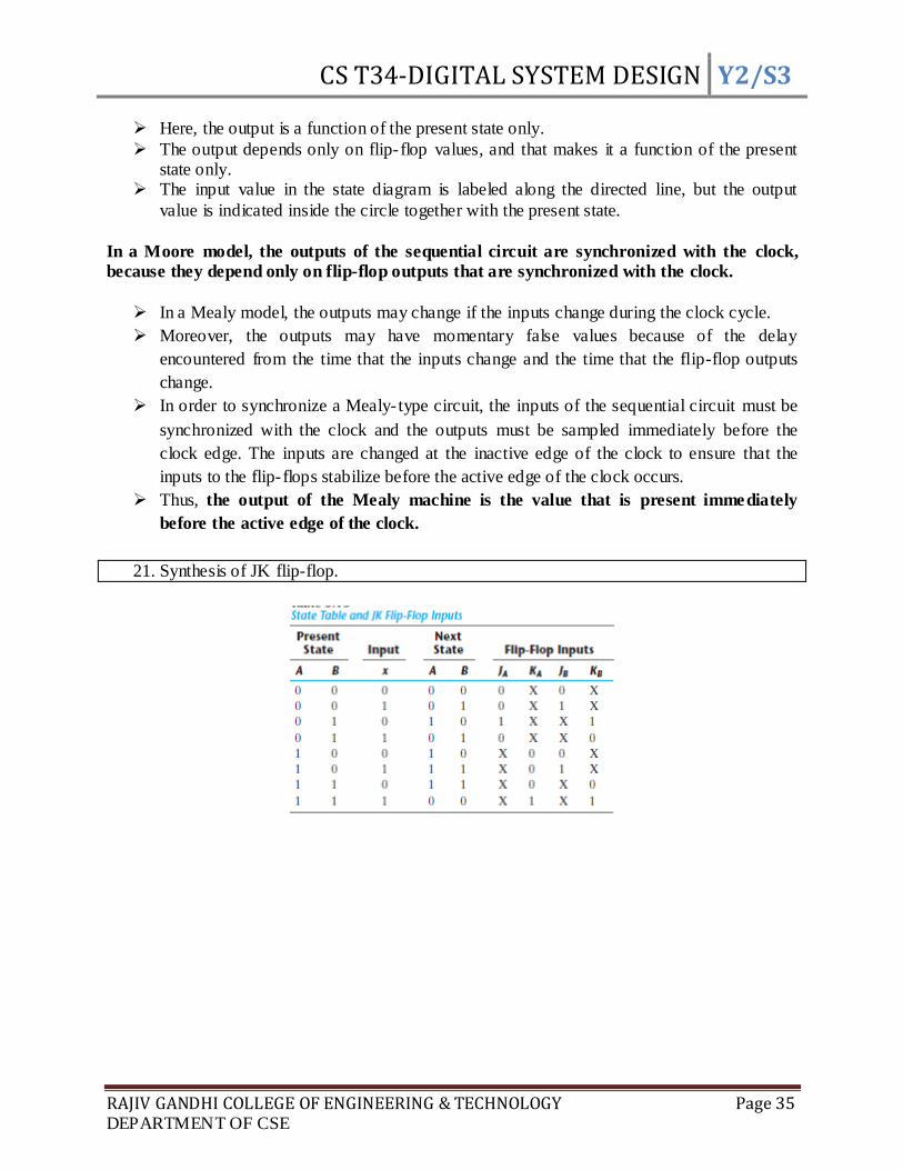
21. Synthesis of JK flip-flop.

CS T34-DIGITAL SYSTEM DESIGN Y2/S3
RAJIV GANDHI COLLEGE OF ENGINEERING & TECHNOLOGY Page 36 DEPARTMENT OF CSE
UNIT III(UNIVERSITY QUESTION)
1. Explain in detail the edge triggered flip-flop. (NOV'12)
2. Explain with neat diagram the serial adder using shift register.
(NOV'12)
3. Explain with a neat diagram the 4-bit bidirectional shift register. (8)
(APR'10)

CS T34-DIGITAL SYSTEM DESIGN Y2/S3
RAJIV GANDHI COLLEGE OF ENGINEERING & TECHNOLOGY Page 37 DEPARTMENT OF CSE
4. Describe the function of shift registers. (11) (APR/MAY'12)
5. With a neat logic diagram explain Master – Slave JK flip-flop.
(11)(NOV'11)
6. Explain in detail the Master – Slave flip – flop. (7) (APR'10)
(6)(APR/MAY'12)
7. Explain with neat diagram the binary up – down counter. (11)
(NOV'11)
8. Describe the design procedure of JK flip-flop.(5) (APR/MAY'12)
9. What is a Flip-Flop? Explain the working principle of D Flip-Flop, T
Flip-Flop in detail. (11) (APR'12)
10. Explain the operation of BCD Ripple counter with necessary diagrams.
(11) (APR'12)
11. Explain the edge triggered D Flip-Flop in detail with neat diagram. (11)
(APR'13)
12. Write in detail about Johnson counter with diagram. (11) (APR'13)
13. Explain in detail about the SR latch. (11) (APR'13 - IT)
14. Describe the working principle of Binary Ripple Counter. (11)
(APR'13 - IT)