stk14c88 32 k x 8 autostore nvsram - usbid · stk14c88 32 k x 8 autostore nvsram cypress...
TRANSCRIPT

STK14C88
32 K x 8 AutoStore nvSRAM
Features
■ 25, 35, 45 ns read access and R/W cycle time
■ Unlimited read/write endurance
■ Automatic nonvolatile STORE on power loss
■ Nonvolatile STORE under hardware or software control
■ Automatic RECALL to SRAM on power up
■ Unlimited RECALL cycles
■ 1-Million STORE cycles
■ 100-year nonvolatile data retention
■ Single 5 V+10% power supply
■ Commercial, industrial, military temperatures
■ 32-Pin 300 mil SOIC (RoHS-compliant)
■ 32-Pin CDIP and LCC packages
Description
The Cypress STK14C88 is a 256 Kb fast static RAM with a nonvolatile Quantum Trap storage element included with each memory cell.
The SRAM provides the fast access and cycle times, ease of use, and unlimited read and write endurance of a normal SRAM.
Data automatically transfers to the nonvolatile storage cells when power loss is detected (the STORE operation). On power up, data is automatically restored to the SRAM (the RECALL operation). Both STORE and RECALL operations are also available under software control.
The Cypress nvSRAM is the first monolithic nonvolatile memory to offer unlimited writes and reads. It is the highest performance, most reliable nonvolatile memory available.
A0 A1 A2 A3 A4 A10
COLUMN I/O
COLUMN DEC
STATIC RAMARRAY
512 x 512
RO
W D
EC
OD
ER
INP
UT
BU
FF
ER
S
Quantum Trap512 x 512
STORE/RECALL
CONTROL
STORE
RECALL
POWERCONTROLA5
A6A7A8A9A11A12A13A14
DQ0
DQ1
DQ2
DQ3DQ4
DQ5DQ6DQ7
SOFTWAREDETECT
G
E
W
HSB
VCCX VCAP
A0 - A13
Logic Block Diagram
Not Rec
ommen
ded f
or New
Des
igns
Cypress Semiconductor Corporation • 198 Champion Court • San Jose, CA 95134-1709 • 408-943-2600Document Number: 001-52038 Rev. *C Revised March 30, 2011
[+] Feedback

STK14C88
Contents
Pin Configurations ........................................................... 3Pin Descriptions ............................................................... 3Absolute Maximum Ratings ............................................ 4DC Characteristics ........................................................... 4AC Test Conditions .......................................................... 5Capacitance ...................................................................... 5SRAM Read Cycles #1 and #2 ......................................... 6SRAM Write Cycle #1 and #2 ........................................... 7Hardware Mode Selection ................................................ 8Hardware STORE Cycle ................................................... 8AutoStore/Power up RECALL ......................................... 9Software STORE/RECALL Mode Selection .................. 10Software-Controlled STORE/RECALL Cycle ................ 10nvSRAM Operation ......................................................... 11Noise Considerations ..................................................... 11SRAM Read .....................................................................11SRAM Write .....................................................................11Power Up RECALL ......................................................... 11Software Nonvolatile STORE ......................................... 11Software Nonvolatile RECALL ...................................... 11
AutoStore Mode .............................................................. 11AutoStore INHIBIT Mode ................................................ 12HSB Operation ................................................................ 12Best Practices ................................................................. 13Preventing STORES ....................................................... 13Hardware Protect ............................................................ 13Low Average Active Power ............................................ 13Ordering Information ...................................................... 14
Commercial and Industrial Ordering Information ....... 14Military Ordering Information ..................................... 15
Package Diagrams .......................................................... 16Acronyms ........................................................................ 19Document Conventions ................................................. 19
Units of Measure ....................................................... 19Document History Page ................................................. 20Sales, Solutions, and Legal Information ...................... 20
Worldwide Sales and Design Support ....................... 20Products .................................................................... 20PSoC Solutions ......................................................... 20
Not Rec
ommen
ded f
or New
Des
igns
Document Number: 001-52038 Rev. *C Page 2 of 20
[+] Feedback

STK14C88
Pin ConfigurationsFigure 1. Pin Diagram - 32-Pin 300 Mil SOIC/CDIP Figure 2. Pin Diagram - 32-Pin 450 Mil LCC
A14
A12
A7
A6
DQ0
DQ1
DQ2
A3
A2
A1
VCAP
A13
A8
A9
A11
A10
DQ7
DQ6
VSS
A0
NC
28
27
26
25
24
23
22
21
20
19
18
17
1
2
3
4
5
6
7
8
9
10
11
12
13
14
15
16
E
A5
NC
A4
32
31
30
29
VCC
HSB
W
DQ5
DQ3
DQ4
G(TOP)
A6
A3
A5
A4
DQ
6
DQ
5
DQ
3
DQ
4
DQ0
A2
A1
A0
DQ
1
DQ
2
VS
S
A10
DQ7
A8
A9
A11
NC
NC
A13
WA14
A12
A7
VC
ap
HS
B
VC
Cx
E
G(TOP)
Pin Descriptions
Pin Name I/O Description
A14-A0 Input Address: The 15 address inputs select one of 32,768 bytes in the nvSRAM array.
DQ7-DQ0 I/O Data: Bi-directional 8-bit data bus for accessing the nvSRAM.
E Input Chip Enable: The active low E input selects the device.
W Input Write Enable: The active low W enables data on the DQ pins to be written to the address location latched by the falling edge of E.
G Input Output Enable: The active low G input enables the data output buffers during read cycles. De-asserting G high caused the DQ pins to tristate.
VCC Power Supply Power: 5.0V, +10%.
HSB I/O Hardware Store Busy: When low this output indicates a Store is in progress. When pulled low external to the chip, it initiates a nonvolatile STORE operation. A weak pull up resistor keeps this pin high if not connected. (optional connection).
VCAP Power Supply AutoStore Capacitor: Supplies power to nvSRAM during power loss to store data from SRAM to nonvolatile storage elements.
VSS Power Supply Ground.
NC No Connect Unlabeled pins have no internal connections.
Not Rec
ommen
ded f
or New
Des
igns
Document Number: 001-52038 Rev. *C Page 3 of 20
[+] Feedback

STK14C88
Absolute Maximum Ratings
Voltage on Input Relative to Ground...............–0.5 V to 7.0 V
Voltage on Input Relative to VSS.........–0.6 V to (VCC + 0.5 V)
Voltage on DQ0-7 or HSB ....................–0.5 V to (VCC + 0.5 V)
Temperature under Bias ............................. –55 C to 125 C
Storage Temperature .................................. –65 C to 150 C
Power Dissipation............................................................ 1 W
DC Output Current (1 output at a time, 1s duration).... 15 mA
Note Stresses greater than those listed under “Absolute Maximum Ratings” may cause permanent damage to the device. This is a stress rating only, and functional operation of the device at conditions above those indicated in the operational sections of this specification is not implied. Exposure to absolute maximum rating conditions for extended periods may affect reliability.
DC CharacteristicsOver the operating range (VCC = 5.0 V ± 10%)[4]
Symbol ParameterCommercial Industrial/
Military Unit NotesMin Max Min Max
ICC1[1] Average VCC Current – 97
8070
– 1008570
mAmAmA
tAVAV = 25 nstAVAV = 35 nstAVAV = 45 ns
ICC2[2] Average VCC Current during
STORE– 3 – 3 mA All Inputs Don’t Care, VCC =
max
ICC3[1] Average VCC Current at tAVAV =
200 ns5V, 25°C, Typical
– 10 – 10 mA W (V CC – 0.2V)All Others Cycling, CMOS Levels
ICC4[2] Average VCAP Current during
AutoStore Cycle– 2 – 2 mA All Inputs Don’t Care
ISB1[3] Average VCC Current
(Standby, Cycling TTL Input Levels)
– 302522
– 312623
mAmAmA
tAVAV = 25 ns, E VIHtAVAV = 35 ns, E VIHtAVAV = 45 ns, E VIH
ISB2[3] VCC Standby Current
(Standby, Stable CMOS Input Levels)
– 1.5 – 1.5 mA E (V CC – 0.2V) All Others VIN 0.2V or (VCC – 0.2V)
IILK Input Leakage Current – 1 – 1 A VCC = maxVIN = VSS to VCC
IOLK Off-State Output Leakage Current – 5 – 5 A VCC = maxVIN = VSS to VCC, E or G VIH
VIH Input Logic “1” Voltage 2.2 VCC + 0.5 2.2 VCC +0.5 V All Inputs
VIL Input Logic “0” Voltage VSS – .5 0.8 VSS – .5 0.8 V All Inputs
VOH Output Logic “1” Voltage 2.4 – 2.4 – V IOUT = – 4 mA except HSB
VOL Output Logic “0” Voltage – 0.4 – 0.4 V IOUT = 8 mA except HSB
VBL Logic “0” Voltage on HSB Output – 0.4 – 0.4 V IOUT = 3 mA
TA Operating Temperature 0 70 -40/-55 85/125 C
Notes1. ICC1 and ICC3 are dependent on output loading and cycle rate. The specified values are obtained with outputs unloaded.2. ICC2 and ICC4 are the average currents required for the duration of the respective STORE cycles (tSTORE).3. E VIH does not produce standby current levels until any nonvolatile cycle in progress has timed out.4. VCC reference levels throughout this data sheet refer to VCC if that is where the power supply connection is made, or VCAP if VCC is connected to ground.
Not Rec
ommen
ded f
or New
Des
igns
Document Number: 001-52038 Rev. *C Page 4 of 20
[+] Feedback

STK14C88
AC Test Conditions
Figure 3. AC Output Loading
Capacitance
Parameter[5] Description Test Conditions Max Unit Conditions
CIN Input Capacitance TA = 25 C, f = 1 MHz, 5 pF V = 0 to 3 V
COUT Output Capacitance 7 pF V = 0 to 3 V
Input pulse levels....................................................0 V to 3 VInput rise and fall times ............................................... <5 nsInput and output timing reference levels ....................... 1.5 V Output load........................................................ See Figure 3
480 Ohms
30 pF255 Ohms
5.0 V
INCLUDINGSCOPE AND
OUTPUT
FIXTURE
Note5. These parameters are guaranteed but not tested.
Not Rec
ommen
ded f
or New
Des
igns
Document Number: 001-52038 Rev. *C Page 5 of 20
[+] Feedback

STK14C88
Figure 5. SRAM Read Cycle 2: E and G Controlled [6]
SRAM Read Cycles #1 and #2
(VCC = 5.0 V ± 10%)[4]
NO.Symbols
ParameterSTK14C88-25 STK14C88-35 STK14C88-45
UnitMin Max Min Max Min Max#1, #2 Alt.
1 tELQV tACS Chip Enable Access Time – 25 – 35 – 45 ns
2 tAVAV[6]
, tELEH[6] tRC Read Cycle Time 25 35 – 45 – ns
3 tAVQV7 tAA Address Access Time – 25 – 35 – 45 ns
4 tGLQV tOE Output Enable to Data Valid – 10 – 15 – 20 ns
5 tAXQX[7] tOH Output Hold after Address Change 5 – 5 – 5 – ns
6 tELQX tLZ Address Change or Chip Enable to Output Active
5 – 5 – 5 – ns
7 tEHQZ[8] tHZ Address Change or Chip Disable to
Output Inactive– 10 – 13 – 15 ns
8 tGLQX tOLZ Output Enable to Output Active 0 – 0 – 0 – ns
9 tGHQZ[8] tOHZ Output Disable to Output Inactive – 10 – 13 15 ns
10 tELICCH[5] tPA Chip Enable to Power Active 0 – 0 0 – ns
11 tEHICCL[5] tPS Chip Disable to Power Standby – 25 35 – 45 ns
Figure 4. SRAM Read Cycle 1: Address Controlled [6, 7]
Notes6. W and HSB must be high during SRAM read cycles.7. I/O state assumes E and G < VIL and W VIH; device is continuously selected.8. Measured ± 200 mV from steady state output voltage.
DATA VALID
5tAXQX
3tAVQV
DQ (DATA OUT)
ADDRESS
2tAVAV
2 29
11
7
9
10
84
3
6
1
Not Rec
ommen
ded f
or New
Des
igns
Document Number: 001-52038 Rev. *C Page 6 of 20
[+] Feedback

STK14C88
SRAM Write Cycle #1 and #2
(VCC = 5.0V ± 10%)[4]
NO.Symbols
ParameterSTK14C88-25 STK14C88-35 STK14C88-45
UnitMin Max Min Max Min Max#1 #2 Alt.
12 tAVAV tAVAV tWC Write Cycle Time 25 – 35 – 45 – ns
13 tWLWH tWLEH tWP Write Pulse Width 20 – 25 – 30 – ns
14 tELWH tELEH tCW Chip Enable to End of Write 20 – 25 – 30 – ns
15 tDVWH tDVEH tDW Data Setup to End of Write 10 – 12 – 15 – ns
16 tWHDX tEHDX tDH Data Hold after End of Write 0 – 0 – 0 – ns
17 tAVWH tAVEH tAW Address Setup to End of Write 20 – 25 – 30 – ns
18 tAVWL tAVEL tAS Address Setup to Start of Write 0 – 0 – 0 – ns
19 tWHAX tEHAX tWR Address Hold after End of Write 0 – 0 – 0 – ns
20 tWLQZ[8, 9] tWZ Write Enable to Output Disable – 10 – 13 – 15 ns
21 tWHQX tOW Output Active after End of Write 5 – 5 – 5 – ns
Figure 6. SRAM Write Cycle 1: W Controlled [10, 11]
Figure 7. SRAM Write Cycle 2: E Controlled [10, 11]
DATA OUT
E
ADDRESS
W
DATA IN
PREVIOUS DATA
12tAVAV
13tWHDX
19tWHAX
13tWLWH
18tAVWL
17tAVWH
DATA VALID20
tWLQZ
15tDVWH
HIGH IMPEDANCE
21tWHQX
14tELWH
12tAVAV
16tEHDX
13tWLEH
19tEHAX
18tAVEL
17tAVEH
DATA VALID
15tDVEH
HIGH IMPEDANCE
14tELEH
DATA OUT
E
ADDRESS
W
DATA IN
Notes9. If W is low when E goes low, the outputs remain in the high impedance state.10. E or W must be VIH during address transitions.11. HSB must be high during SRAM write cycles.
Not Rec
ommen
ded f
or New
Des
igns
Document Number: 001-52038 Rev. *C Page 7 of 20
[+] Feedback
STK14C88
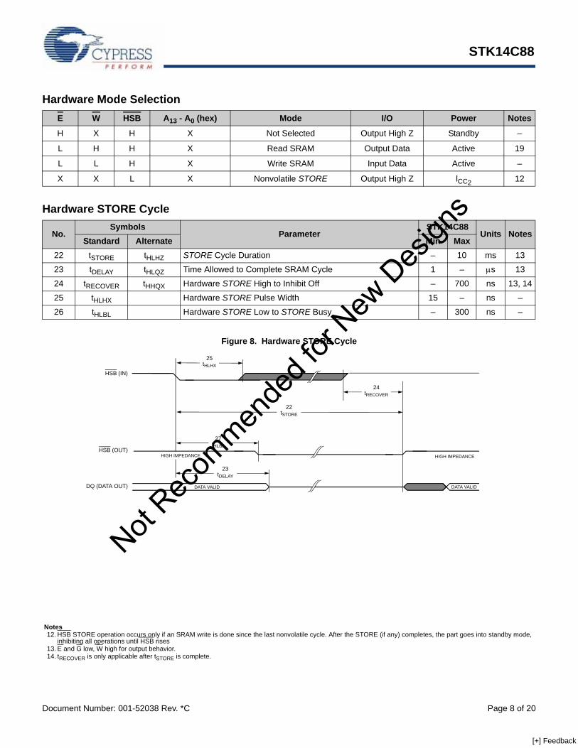
Hardware Mode Selection
E W HSB A13 - A0 (hex) Mode I/O Power Notes
H X H X Not Selected Output High Z Standby –
L H H X Read SRAM Output Data Active 19
L L H X Write SRAM Input Data Active –
X X L X Nonvolatile STORE Output High Z lCC2 12
Hardware STORE Cycle
No.Symbols
ParameterSTK14C88
Units NotesStandard Alternate Min Max
22 tSTORE tHLHZ STORE Cycle Duration – 10 ms 13
23 tDELAY tHLQZ Time Allowed to Complete SRAM Cycle 1 – s 13
24 tRECOVER tHHQX Hardware STORE High to Inhibit Off – 700 ns 13, 14
25 tHLHX Hardware STORE Pulse Width 15 – ns –
26 tHLBL Hardware STORE Low to STORE Busy – 300 ns –
Figure 8. Hardware STORE Cycle
DATA VALID
HSB (IN)
DATA VALID
25tHLHX
23tDELAY
22tSTORE
24tRECOVER
HIGH IMPEDANCE
27tHLBL
HIGH IMPEDANCE
DQ (DATA OUT)
HSB (OUT)
Notes12. HSB STORE operation occurs only if an SRAM write is done since the last nonvolatile cycle. After the STORE (if any) completes, the part goes into standby mode,
inhibiting all operations until HSB rises13. E and G low, W high for output behavior.14. tRECOVER is only applicable after tSTORE is complete.
Not Rec
ommen
ded f
or New
Des
igns
Document Number: 001-52038 Rev. *C Page 8 of 20
[+] Feedback

STK14C88
AutoStore/Power up RECALL
NO.Symbols
ParameterSTK14C88
Unit NotesStandard Alt. Min Max
27 tRESTORE Power up RECALL Duration – 550 s 15
28 tSTORE tHLHZ STORE Cycle Duration – 10 ms 13, 16
29 tVSBL Low Voltage Trigger (VSWITCH) to HSB Low
– 300 ns 11
30 tDELAY tBLQZ Time Allowed to Complete SRAM Cycle
1 – s 13
31 VSWITCH Low Voltage Trigger Level 4.0 4.5 V –
32 VRESET Low Voltage Reset Level – 3.6 V –
Figure 9. AutoStore/POWER UP RECALL
31tDELAY
30tVSBL
POWER UP RECALL
BROWN OUTNO STORE
(NO SRAM Writes)
NO RECALL(VCC DID NOT GO BELOW VRESET)
BROWN OUTAutoStore
NO RECALL(VCC DID NOT GO BELOW VRESET)
BROWN OUTAutoStore
RECALL WHENVCC RETURNS
ABOVE VSWITCH
AutoStore
HSB
W
29tSTORE
28tRESTORE
POWER UP RECALL
31VSWITCH
27VRESET
VCC
DQ (DATA OUT)
Notes15. tRESTORE starts from the time VCC rises above VSWITCH.16. HSB is asserted low for 1s when VCAP drops through VSWITCH. If an SRAM write has not taken place since the last nonvolatile cycle, HSB is released and no STORE
takes place.
Not Rec
ommen
ded f
or New
Des
igns
Document Number: 001-52038 Rev. *C Page 9 of 20
[+] Feedback

STK14C88
Software STORE/RECALL Mode Selection
E W A13 - A0 (hex) Mode I/O POWER Notes
L H 0E3831C703E03C1F303F
Read SRAMRead SRAMRead SRAMRead SRAMRead SRAM
Output DataOutput DataOutput DataOutput DataOutput Data
Active
13, 17, 18, 19
0FC0 Nonvolatile STORE Output High Z ICC2
L H 0E3831C703E03C1F303F0C63
Read SRAMRead SRAMRead SRAMRead SRAMRead SRAM
Nonvolatile RECALL
Output DataOutput DataOutput DataOutput DataOutput Data
Output High Z
Active 13, 17, 18, 19
Software-Controlled STORE/RECALL Cycle
NO. Symbols Parameter STK14C88-25 STK14C88-35 STK14C88-45 Unit Notes
Standard Alt. Min Max Min Max Min Max
33 tAVAV tRC STORE/RECALL Initiation Cycle Time 35 – 45 – 55 – ns 13
34 tAVEL tAS Address Setup Time 0 – 0 – 0 – ns 20, 21
35 tELEH tCW Clock Pulse Width 25 – 30 – 35 – ns 20, 21
36 tELAX Address Hold Time 20 – 20 – 20 – ns 20, 21
37 tRECALL RECALL Duration – 20 – 20 – 20 s –
Figure 10. E Controlled Software STORE/RECALL Cycle [21]
Notes17. The six consecutive addresses must be in the order listed. W must be high during all six consecutive E controlled cycles to enable a nonvolatile cycle.18. While there are 15 addresses on the STK14C88, only the lower 14 are used to control software modes.19. I/O state assumes G < VIL. Activation of nonvolatile cycles does not depend on state of G.20. The software sequence is clocked on the falling edge of E controlled reads without involving G (double clocking aborts the sequence). 21. The six consecutive addresses must be in the order listed in the Software STORE/RECALL Mode Selection Table: (0E38, 31C7, 03E0, 3C1F, 303F, 0FC0) for a STORE
cycle or (0E38, 31C7, 03E0, 3C1F, 303F, 0C63) for a RECALL cycle. W must be high during all six consecutive cycles.
DATA VALIDHIGH IMPEDANCE
ADDRESS #6ADDRESS #1
DATA VALID
33tAVAV
DATA VALIDDQ (DATA
E
ADDRESS
29 37tSTORE / tRECALL
33tAVAV
34tAVEL
35tELEH
36tELAX
Not Rec
ommen
ded f
or New
Des
igns
Document Number: 001-52038 Rev. *C Page 10 of 20
[+] Feedback

STK14C88
nvSRAM Operation
The STK14C88 has two separate modes of operation: SRAM mode and nonvolatile mode. In SRAM mode, the memory operates as a standard fast static RAM. In nonvolatile mode, data is transferred from SRAM to nonvolatile elements (the STORE operation) or from nonvolatile elements to SRAM (the RECALL operation). In this mode, SRAM functions are disabled.
Noise Considerations
The STK14C88 is a high speed memory and so must have a high frequency bypass capacitor of approximately 0.1 F connected between VCAP and VSS, using leads and traces that are as short as possible. As with all high speed CMOS ICs, careful routing of power, ground, and signals helps to prevent noise problems.
SRAM Read
The STK14C88 performs a read cycle whenever E and G are low, and W and HSB are high. The address specified on pins A0-14 determines which of the 32,768 data bytes are accessed. When the read is initiated by an address transition, the outputs are valid after a delay of tAVQV (Read cycle #1). If the read is initiated by E or G, the outputs are valid at tELQV or at tGLQV, whichever is later (Read cycle #2). The data outputs repeatedly respond to address changes within the tAVQV access time without the need for transitions on any control input pins, and remain valid until another address change or until E or G is brought high, or W or HSB is brought low.
SRAM Write
A write cycle is performed whenever E and W are low, and HSB is high. The address inputs must be stable prior to entering the write cycle and must remain stable until either E or W goes high at the end of the cycle. The data on the common I/O pins DQ0-7 are written into the memory if it is valid tDVWH before the end of a W controlled write or tDVEH before the end of an E controlled write.
Keep G high during the entire write cycle to avoid data bus contention on common I/O lines. If G is left low, internal circuitry turns off the output buffers tWLQZ after W goes low.
Power Up RECALL
During power up, or after any low power condition (VCAP < VRESET), an internal RECALL request is latched. When VCAP again exceeds the sense voltage of VSWITCH, a RECALL cycle is automatically initiated and takes tRESTORE to complete.
If the STK14C88 is in a write state at the end of power up RECALL, the SRAM data will be corrupted. To avoid this, a 10 KOhm resistor should be connected either between W and system VCC or between E and system VCC.
Software Nonvolatile STORE
The STK14C88 software STORE cycle is initiated by executing sequential E controlled read cycles from six specific address locations. During the STORE cycle an erase of the previous nonvolatile data is first performed, followed by a program of the nonvolatile elements. The program operation copies the SRAM data into nonvolatile memory. When a STORE cycle is initiated, further input and output are disabled until the cycle is completed.
Because a sequence of reads from specific addresses is used for STORE initiation, it is important that no other read or write accesses intervene in the sequence, or the sequence will be aborted and no STORE or RECALL takes place.
To initiate the software STORE cycle, the following read sequence must be performed:
1. Read address 0E38 (hex) Valid READ
2. Read address 31C7 (hex) Valid READ
3. Read address 03E0 (hex) Valid READ
4. Read address 3C1F (hex) Valid READ
5. Read address 303F (hex) Valid READ
6. Read address 0FC0 (hex) Initiate STORE cycle
The software sequence must be clocked with E controlled reads.
After the sixth address in the sequence is entered, the STORE cycle commences and the chip is disabled. Use only read cycles in the sequence, although it is not necessary that G be low for the sequence to be valid. After the tSTORE cycle time is fulfilled, the SRAM is again activated for read and write operation.
Software Nonvolatile RECALL
A software RECALL cycle is initiated with a sequence of read operations in a manner similar to the software STORE initiation. To initiate the RECALL cycle, the following sequence of E controlled read operations must be performed:
1. Read address 0E38 (hex) Valid READ
2. Read address 31C7 (hex) Valid READ
3. Read address 03E0 (hex) Valid READ
4. Read address 3C1F (hex) Valid READ
5. Read address 303F (hex) Valid READ
6. Read address 0C63 (hex) Initiate RECALL cycle
Internally, RECALL is a two step procedure. First, the SRAM data is cleared, and second, the nonvolatile information is transferred into the SRAM cells. After the tRECALL cycle time, the SRAM is again ready for read and write operations. The RECALL operation in no way alters the data in the nonvolatile elements. The nonvolatile data can be recalled an unlimited number of times.
AutoStore Mode
The STK14C88 can be powered in one of three modes.
During normal AutoStore operation, the STK14C88 draws current from VCC to charge a capacitor connected to the VCAP pin. This stored charge is used by the chip to perform a single STORE operation. After power up, when the voltage on the VCAP pin drops below VSWITCH, the part automatically disconnects the VCAP pin from VCC and initiate a STORE operation.
Not Rec
ommen
ded f
or New
Des
igns
Document Number: 001-52038 Rev. *C Page 11 of 20
[+] Feedback

STK14C88
Figure 11 shows the proper connection of capacitors for automatic store operation. A charge storage capacitor having a capacity of between 68 µF and 220 µF (±20%) rated at 6V should be provided. In system power mode, both VCC and VCAP are connected to the + 5V power supply without the 68 µF capacitor. In this mode, the AutoStore function of the STK14C88 operates on the stored system charge as power goes down. The user must, however, guarantee that VCC does not drop below 3.6V during the 10 ms STORE cycle. If an automatic STORE on power loss is not required, then VCC can be tied to ground and + 5V applied to VCAP (Figure 12). This is the AutoStore Inhibit mode, in which the AutoStore function is disabled. If the STK14C88 is operated in this configuration, refer-ences to VCC should be changed to VCAP throughout this data sheet. In this mode, STORE operations may be triggered through software control or the HSB pin. To enable or disable AutoStore using an I/O port pin, see Preventing STORES on page 13.
To prevent unneeded STORE operations, automatic STOREs and those initiated by externally driving HSB low are ignored unless at least one write operation has taken place since the most recent STORE or RECALL cycle. Software initiated STORE cycles are performed regardless of whether a write operation has taken place.
If the power supply drops faster than 20 ms/volt before VCC reaches VSWITCH, then a 2.2 ohm resistor should be inserted between VCC and the system supply to avoid momentary excess of current between Vcc and VCAP.
Figure 11. AutoStore Mode
AutoStore INHIBIT Mode
If an automatic STORE on power loss is not required, then VCC can be tied to ground and system power applied to VCAP (Figure 12). This is the AutoStore Inhibit mode, in which the AutoStore function is disabled. If the STK14C88 is operated in this config-uration, references to VCC should be changed to VCAP throughout this data sheet. In this mode, STORE operations may be triggered through software control. It is not permissible to change between these three options “on the fly.”
Figure 12. AutoStore Inhibit Mode
HSB Operation
The STK14C88 provides the HSB pin for controlling and acknowledging the STORE operations. The HSB pin can be used to request a hardware STORE cycle. When the HSB pin is driven low, the STK14C88 conditionally initiates a STORE operation after tDELAY; an actual STORE cycle only begins if a write to the SRAM took place since the last STORE or RECALL cycle. The HSB pin has a very resistive pull up and is internally driven low to indicate a busy condition when the STORE (initiated by any means) is in progress. Pull up this pin with an external 10 Kohm resistor to VCAP if HSB is used as a driver.
SRAM read and write operations that are in progress when HSB is driven low by any means are given time to complete before the STORE operation is initiated. After HSB goes low, the STK14C88 continues SRAM operations for tDELAY. During tDELAY, multiple SRAM read operations may take place. If a write is in progress when HSB is pulled low it is allowed a time, tDELAY, to complete. However, any SRAM write cycles requested after HSB goes low are inhibited until HSB returns high.
The HSB pin can be used to synchronize multiple STK14C88s while using a single larger capacitor. To operate in this mode, the HSB pin should be connected together to the HSB pins from the other STK14C88s. An external pull up resistor to + 5V is required because HSB acts as an open drain pull down. The VCAP pins from the other STK14C88 parts can be tied together and share a single capacitor. The capacitor size must be scaled by the number of devices connected to it. When any one of the STK14C88s detects a power loss and asserts HSB, the common HSB pin causes all parts to request a STORE cycle (a STORE takes place in those STK14C88s that are written since the last nonvolatile cycle).
During any STORE operation, regardless of how it was initiated, the STK14C88 continues to drive the HSB pin low, releasing it only when the STORE is complete. Upon completion of the STORE operation the STK14C88 remains disabled until the HSB pin returns high.
If HSB is not used, leave it unconnected.
1
16
32
31
17
68
F6v
, ±20
%
0.1
FB
ypass
30
+
10k
10k
17
1
16
32
31
30
Byp
ass
0.1
µF
10
K?
10K
?
Not Rec
ommen
ded f
or New
Des
igns
Document Number: 001-52038 Rev. *C Page 12 of 20
[+] Feedback

STK14C88
Best Practices
nvSRAM products have been used effectively for over 15 years. While ease-of-use is one of the product’s main system values, experience gained working with hundreds of applications has resulted in the following suggestions as best practices:
■ The nonvolatile cells in an nvSRAM are programmed on the test floor during final test and quality assurance. Incoming inspection routines at customer or contract manufacturer’s sites sometimes reprogram these values. Final NV patterns are typically repeating patterns of AA, 55, 00, FF, A5, or 5A. The end product’s firmware should not assume an NV array is in a set programmed state. Routines that check memory content values to determine first time system configuration, cold or warm boot status, and so on should always program a unique NV pattern (for example, complex 4-byte pattern of 46 E6 49 53 hex or more random bytes) as part of the final system manufacturing test to ensure these system routines work consistently.
■ Power up boot firmware routines should rewrite the nvSRAM into the desired state (such as autostore enabled). While the nvSRAM is shipped in a preset state, best practice is to again rewrite the nvSRAM into the desired state as a safeguard against events that might flip the bit inadvertently (program bugs, incoming inspection routines, and so on).
■ The VCAP value specified in this data sheet includes a minimum and a maximum value size. Best practice is to meet this requirement and not exceed the max VCAP value because the nvSRAM internal algorithm calculates VCAP charge time based on this max VCAP value. Customers who want to use a larger VCAP value to make sure there is extra store charge and store time should discuss their VCAP size selection with Cypress to understand any impact on the VCAP voltage level at the end of a tRECALL period.
Preventing STORES
The STORE function can be disabled on the fly by holding HSB high with a driver capable of sourcing 30 mA at a VOH of at least 2.2V, because it must overpower the internal pull down device that drives HSB low for 20 ms at the onset of a STORE. When the STK14C88 is connected for AutoStore operation (system VCC connected to VCC and a 68 uF capacitor on VCAP) and VCC crosses VSWITCH on the way down, the STK14C88 attempts to pull HSB low; if HSB does not actually get below VIL, the part stops trying to pull HSB low and abort the STORE attempt.
Hardware Protect
The STK14C88 offers hardware protection against inadvertent STORE operation and SRAM writes during low voltage condi-tions. When VCAP < VSWITCH, all externally initiated STORE operations and SRAM writes are inhibited.
AutoStore can be completely disabled by tying VCC to ground and applying + 5V to VCAP. This is the AutoStore Inhibit mode; in this mode STOREs are only initiated by explicit request using either the software sequence or the HSB pin.
Low Average Active Power
The STK14C88 draws significantly less current when it is cycled at times longer than 50 ns. Figure 13 shows the relationship between ICC and read cycle time. Worst case current consumption is shown for both CMOS and TTL input levels (commercial temperature range, VCC = 5.5V, 100% duty cycle on chip enable). Figure 14 shows the same relationship for write cycles. If the chip enable duty cycle is less than 100%, only standby current is drawn when the chip is disabled. The overall average current drawn by the STK14C88 depends on the following items:
■ CMOS vs. TTL input levels
■ The duty cycle of chip enable
■ The overall cycle rate for accesses
■ The ratio of reads to writes
■ The operating temperature
■ The VCC level
■ I/O loading.
Figure 13. Icc (max) Reads
Figure 14. Icc (max) Writes
0
20
40
60
80
100
50 100 150 200Cycle Time (ns)
TTL
CMOS
Ave
rage
Act
ive
Cur
rent
(m
A)
0
20
40
60
80
100
50 100 150 200Cycle Time (ns)
TTL
CMOS
Ave
rage
Act
ive
Cur
rent
(m
A)Not
Recom
mende
d for
New D
esign
s
Document Number: 001-52038 Rev. *C Page 13 of 20
[+] Feedback

STK14C88
Ordering Information
These parts are not recommended for new designs.
Part Number Description Access Times Temperature
STK14C88-NF25 5V 32Kx8 AutoStore nvSRAM SOIC32-300 25 ns Commercial
STK14C88-NF35 5V 32Kx8 AutoStore nvSRAM SOIC32-300 35 ns Commercial
STK14C88-NF45 5V 32Kx8 AutoStore nvSRAM SOIC32-300 45 ns Commercial
STK14C88-NF25TR 5V 32Kx8 AutoStore nvSRAM SOIC32-300 25 ns Commercial
STK14C88-NF35TR 5V 32Kx8 AutoStore nvSRAM SOIC32-300 35 ns Commercial
STK14C88-NF45TR 5V 32Kx8 AutoStore nvSRAM SOIC32-300 45 ns Commercial
STK14C88-NF25I 5V 32Kx8 AutoStore nvSRAM SOIC32-300 25 ns Industrial
STK14C88-NF35I 5V 32Kx8 AutoStore nvSRAM SOIC32-300 35 ns Industrial
STK14C88-NF45I 5V 32Kx8 AutoStore nvSRAM SOIC32-300 45 ns Industrial
STK14C88-NF25ITR 5V 32Kx8 AutoStore nvSRAM SOIC32-300 25 ns Industrial
STK14C88-NF35ITR 5V 32Kx8 AutoStore nvSRAM SOIC32-300 35 ns Industrial
STK14C88-NF45ITR 5V 32Kx8 AutoStore nvSRAM SOIC32-300 45 ns Industrial
STK14C88-C45I 5V 32Kx8 AutoStore nvSRAM CDIP32-300 45 ns Industrial
STK14C88-5L35M 5V 32Kx8 AutoStore nvSRAM LCC32-300 35 ns Military
STK14C88-5L45M 5V 32Kx8 AutoStore nvSRAM LCC32-300 45 ns Military
STK14C88-5C35M 5V 32Kx8 AutoStore nvSRAM CDIP32-300 35 ns Military
STK14C88-5C45M 5V 32Kx8 AutoStore nvSRAM CDIP32-300 45 ns Military
STK14C88-5K35M 5V 32Kx8 AutoStore nvSRAM CDIP32-300 35 ns Military
STK14C88-5K45M 5V 32Kx8 AutoStore nvSRAM CDIP32-300 45 ns Military
Commercial and Industrial Ordering Information
Speed:25 = 25 ns35 = 35 ns
STK14C88 - N F 45 I TR
Temperature Range:
Package
45 = 45 ns
Packaging Option:Blank = TubeTR = Tape and Reel
I - Industrial (-40 to 85°C)Blank = Commercial (0 to 70°C)
Lead FinishF = 100% Sn (Matte Tin)
N = Plastic 32-pin 300 mil SOICC = Ceramic 32-pin 300 mil CDIPL = Ceramic 32-pad LCC
Not Rec
ommen
ded f
or New
Des
igns
Document Number: 001-52038 Rev. *C Page 14 of 20
[+] Feedback

STK14C88
Military Ordering Information
Access Time
STK14C88 - 5 C 45 M
Temperature Range
M = Military (-55 to 125C)
35 = 35 ns45 = 45 ns
PackageL=Ceramic 32-pad LCCC=Ceramic 32-pin 300 mil CDIPK=Ceramic 32-pin 300 mil CDIP with solder dip finish
Retention / Endurance5 = Military (105 Cycles)
Not Rec
ommen
ded f
or New
Des
igns
Document Number: 001-52038 Rev. *C Page 15 of 20
[+] Feedback

STK14C88
Package DiagramsFigure 15. 32-Pin 300 mil SOIC Gull Wing (51-85127)
PIN 1 ID
SEATING PLANE
116
17 32
DIMENSIONS IN INCHES[MM] MIN.MAX.
0.292[7.416]0.299[7.594]
0.405[10.287]0.419[10.642]
0.050[1.270]TYP.
0.090[2.286]0.100[2.540]
0.004[0.101]0.0100[0.254]
0.006[0.152]0.012[0.304]
0.021[0.533]0.041[1.041]
0.026[0.660]0.032[0.812]
0.004[0.101]
REFERENCE JEDEC MO-119
PART #
S32.3 STANDARD PKG.SZ32.3 LEAD FREE PKG.
0.014[0.355]0.020[0.508]
0.810[20.574]0.822[20.878]
51-85127 *B
Not Rec
ommen
ded f
or New
Des
igns
Document Number: 001-52038 Rev. *C Page 16 of 20
[+] Feedback

STK14C88
Figure 16. 32-Pin 300 mil Side Braze DIL (001-51694)
Package Diagrams (continued)
001-51694 *A
Not Rec
ommen
ded f
or New
Des
igns
Document Number: 001-52038 Rev. *C Page 17 of 20
[+] Feedback

STK14C88
Figure 17. 32-Pin 450 mil Ceramic LCC (51-80068)
Package Diagrams (continued)
.045
.055
.055
.045
.045
.055
.064
.090
.442
.458
.540
.560
.022
.028
PIN 1
.009 R.32 PLACES
DIMENSIONS IN INCHESMIN.MAX.
.080
.060
51-80068 *A
Not Rec
ommen
ded f
or New
Des
igns
Document Number: 001-52038 Rev. *C Page 18 of 20
[+] Feedback

STK14C88
Acronyms Document Conventions
Units of MeasureAcronym Description
nvSRAM nonvolatile static random access memory
SSOP shrink small-outline package
SOIC small-outline integrated circuit
TSOP II thin small outline package
FBGA fine-pitch ball grid array
RoHS restriction of hazardous substances
I/O input/output
CMOS complementary metal oxide semiconductor
EIA electronic industries alliance
RWI read and write inhibited
Symbol Unit of Measure
°C degrees celsius
Hz hertz
kbit 1024 bits
kHz kilohertz
K kilo ohms
A microamperes
mA milliampere
F microfarads
MHz megahertz
s microseconds
ms millisecond
ns nanoseconds
pF picofarads
V volts
ohms
W watts
Not Rec
ommen
ded f
or New
Des
igns
Document Number: 001-52038 Rev. *C Page 19 of 20
[+] Feedback

STK14C88
© Cypress Semiconductor Corporation, 2009-2011. The information contained herein is subject to change without notice. Cypress Semiconductor Corporation assumes no responsibility for the use ofany circuitry other than circuitry embodied in a Cypress product. Nor does it convey or imply any license under patent or other rights. Cypress products are not warranted nor intended to be used formedical, life support, life saving, critical control or safety applications, unless pursuant to an express written agreement with Cypress. Furthermore, Cypress does not authorize its products for use ascritical components in life-support systems where a malfunction or failure may reasonably be expected to result in significant injury to the user. The inclusion of Cypress products in life-support systemsapplication implies that the manufacturer assumes all risk of such use and in doing so indemnifies Cypress against all charges.
Any Source Code (software and/or firmware) is owned by Cypress Semiconductor Corporation (Cypress) and is protected by and subject to worldwide patent protection (United States and foreign),United States copyright laws and international treaty provisions. Cypress hereby grants to licensee a personal, non-exclusive, non-transferable license to copy, use, modify, create derivative works of,and compile the Cypress Source Code and derivative works for the sole purpose of creating custom software and or firmware in support of licensee product to be used only in conjunction with a Cypressintegrated circuit as specified in the applicable agreement. Any reproduction, modification, translation, compilation, or representation of this Source Code except as specified above is prohibited withoutthe express written permission of Cypress.
Disclaimer: CYPRESS MAKES NO WARRANTY OF ANY KIND, EXPRESS OR IMPLIED, WITH REGARD TO THIS MATERIAL, INCLUDING, BUT NOT LIMITED TO, THE IMPLIED WARRANTIESOF MERCHANTABILITY AND FITNESS FOR A PARTICULAR PURPOSE. Cypress reserves the right to make changes without further notice to the materials described herein. Cypress does notassume any liability arising out of the application or use of any product or circuit described herein. Cypress does not authorize its products for use as critical components in life-support systems wherea malfunction or failure may reasonably be expected to result in significant injury to the user. The inclusion of Cypress’ product in a life-support systems application implies that the manufacturerassumes all risk of such use and in doing so indemnifies Cypress against all charges.
Use may be limited by and subject to the applicable Cypress software license agreement.
Document History Page
Sales, Solutions, and Legal Information
Worldwide Sales and Design Support
Cypress maintains a worldwide network of offices, solution centers, manufacturer’s representatives, and distributors. To find the office closest to you, visit us at Cypress Locations.
Products
Automotive cypress.com/go/automotive
Clocks & Buffers cypress.com/go/clocks
Interface cypress.com/go/interface
Lighting & Power Control cypress.com/go/powerpsoc
cypress.com/go/plc
Memory cypress.com/go/memory
Optical & Image Sensing cypress.com/go/image
PSoC cypress.com/go/psoc
Touch Sensing cypress.com/go/touch
USB Controllers cypress.com/go/USB
Wireless/RF cypress.com/go/wireless
PSoC Solutions
psoc.cypress.com/solutions
PSoC 1 | PSoC 3 | PSoC 5
Document Title: STK14C88 32 K x 8 AutoStore nvSRAMDocument Number: 001-52038
Rev. ECN No. Orig. of Change Submission Date Description of Change
** 2668632 GVCH 03/04/2009 New data sheet
*A 2718242 GVCH 06/12/09 Ordering Information description: Corrected typo
*B 2821358 GVCH 12/04/2009 Added Note in Ordering Information mentioning that these parts are not recommended for new designs.Added “Not recommended for New Designs” watermark in the PDF.Added Contents on page 2.
*C 3210316 GVCH 03/30/2011 Moved contents of page 14 to page 10.Updated package diagram.Added Acronyms and Document Conventions.
Not Rec
ommen
ded f
or New
Des
igns
Document Number: 001-52038 Rev. *C Revised March 30, 2011 Page 20 of 20
All products and company names mentioned in this document may be the trademarks of their respective holders.
[+] Feedback