spice model of tpcp8401 (professional+bdp n&p model) in spice park
DESCRIPTION
SPICE MODEL of TPCP8401 (Professional+BDP N&P Model) in SPICE PARK. English Version is http://www.spicepark.net. Japanese Version is http://www.spicepark.com by Bee Technologies.TRANSCRIPT
All Rights Reserved Copyright (c) Bee Technologies Inc. 2006
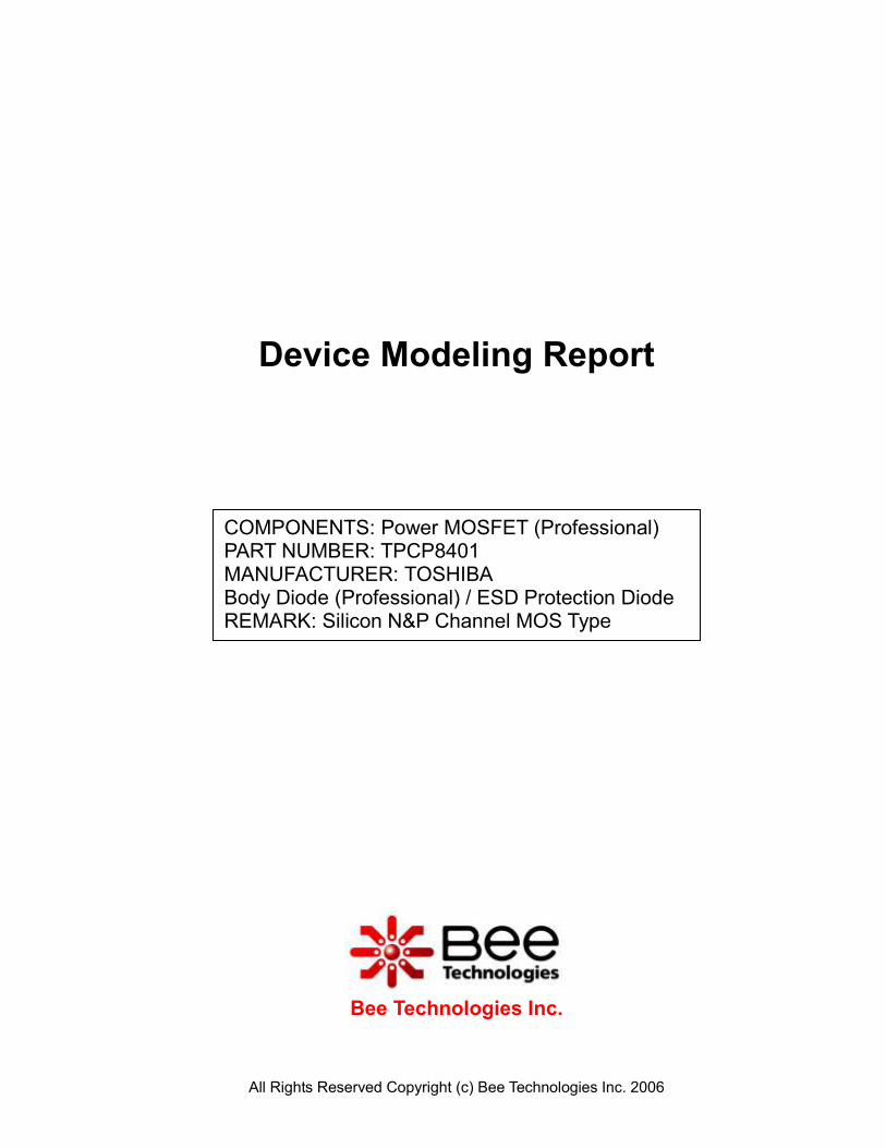
Device Modeling Report
Bee Technologies Inc.
COMPONENTS: Power MOSFET (Professional) PART NUMBER: TPCP8401 MANUFACTURER: TOSHIBA Body Diode (Professional) / ESD Protection Diode REMARK: Silicon N&P Channel MOS Type
All Rights Reserved Copyright (c) Bee Technologies Inc. 2006
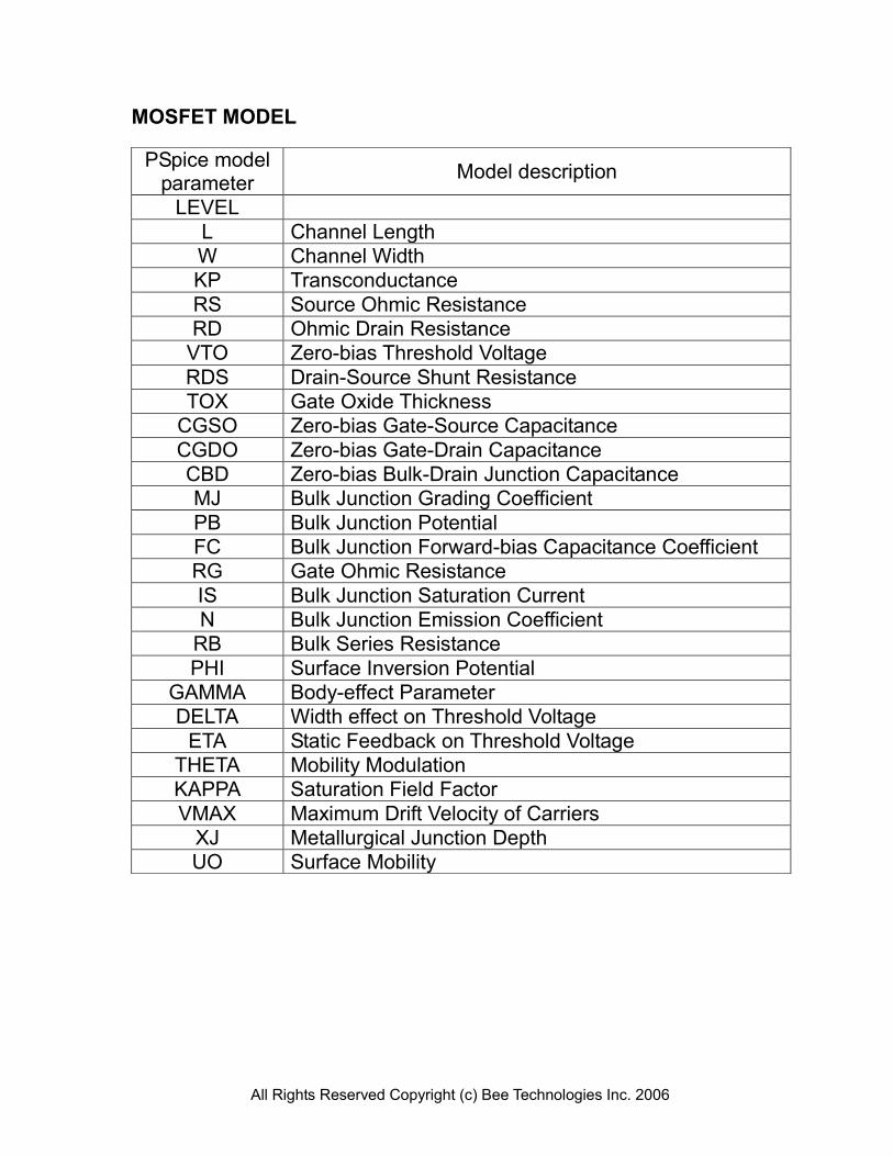
MOSFET MODEL
PSpice model parameter
Model description
LEVEL
L Channel Length
W Channel Width
KP Transconductance
RS Source Ohmic Resistance
RD Ohmic Drain Resistance
VTO Zero-bias Threshold Voltage
RDS Drain-Source Shunt Resistance
TOX Gate Oxide Thickness
CGSO Zero-bias Gate-Source Capacitance
CGDO Zero-bias Gate-Drain Capacitance
CBD Zero-bias Bulk-Drain Junction Capacitance
MJ Bulk Junction Grading Coefficient
PB Bulk Junction Potential
FC Bulk Junction Forward-bias Capacitance Coefficient
RG Gate Ohmic Resistance
IS Bulk Junction Saturation Current
N Bulk Junction Emission Coefficient
RB Bulk Series Resistance
PHI Surface Inversion Potential
GAMMA Body-effect Parameter
DELTA Width effect on Threshold Voltage
ETA Static Feedback on Threshold Voltage
THETA Mobility Modulation
KAPPA Saturation Field Factor
VMAX Maximum Drift Velocity of Carriers
XJ Metallurgical Junction Depth
UO Surface Mobility
All Rights Reserved Copyright (c) Bee Technologies Inc. 2006
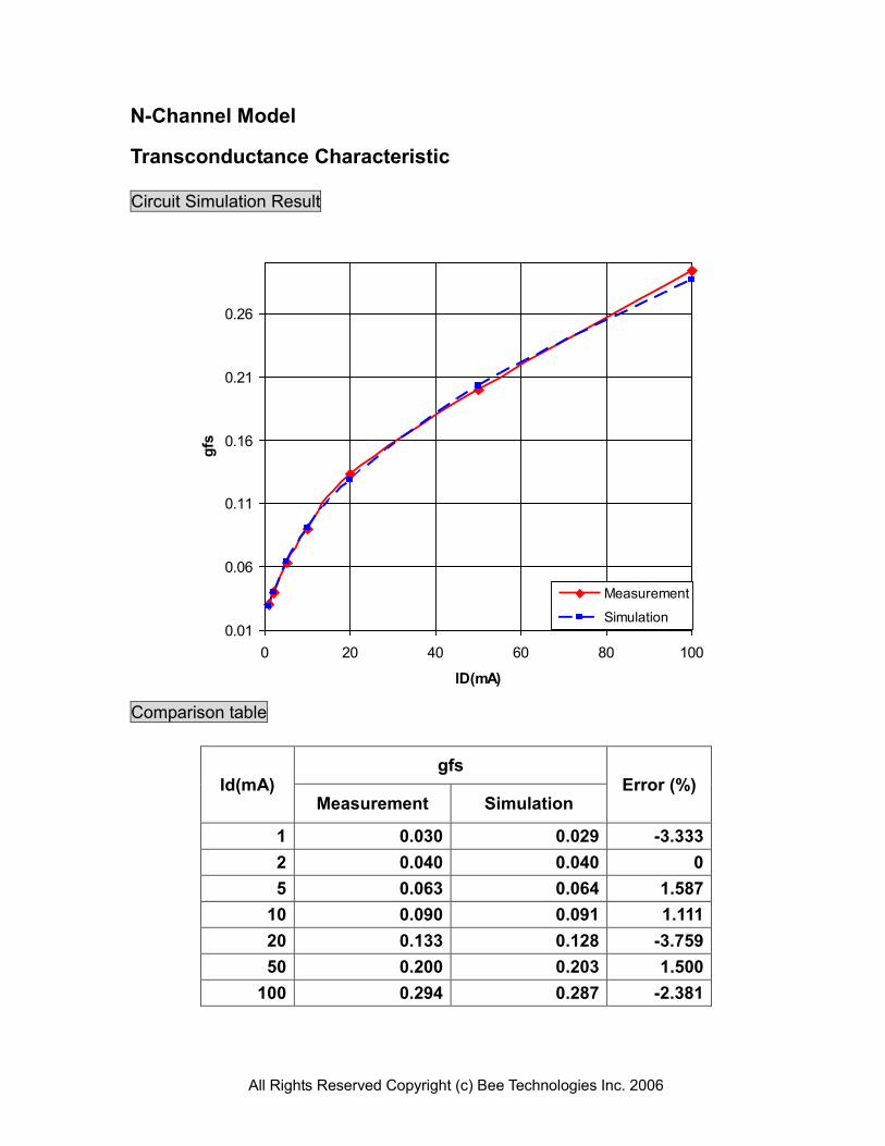
0.01
0.06
0.11
0.16
0.21
0.26
0 20 40 60 80 100
ID(mA)
gfs
Measurement
Simulation
N-Channel Model
Transconductance Characteristic
Circuit Simulation Result
Comparison table
Id(mA) gfs
Error (%) Measurement Simulation
1 0.030 0.029 -3.333
2 0.040 0.040 0
5 0.063 0.064 1.587
10 0.090 0.091 1.111
20 0.133 0.128 -3.759
50 0.200 0.203 1.500
100 0.294 0.287 -2.381
All Rights Reserved Copyright (c) Bee Technologies Inc. 2006
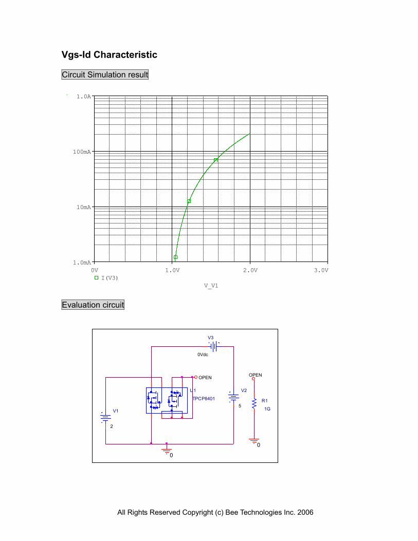
OPEN
0
V2
5R1
1G
V3
0Vdc
OPEN
U1
TPCP8401
V1
2
0
V_V1
0V 1.0V 2.0V 3.0V
I(V3)
1.0mA
10mA
100mA
1.0A
Vgs-Id Characteristic
Circuit Simulation result
Evaluation circuit
All Rights Reserved Copyright (c) Bee Technologies Inc. 2006
1
10
100
0 1 2 3
VGS - Gate to Source Voltage - V
ID -
Dra
in C
urr
en
t (m
A)
Measurement
Simulation
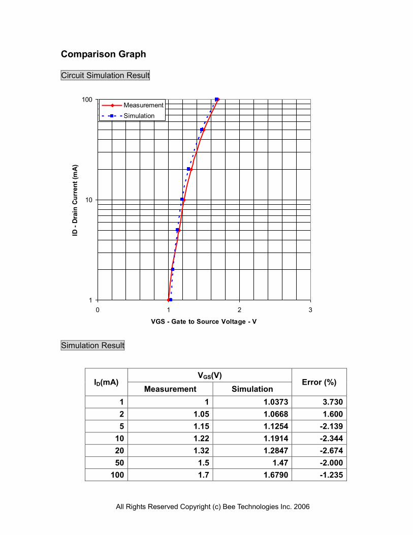
Comparison Graph Circuit Simulation Result
Simulation Result
ID(mA) VGS(V)
Error (%) Measurement Simulation
1 1 1.0373 3.730
2 1.05 1.0668 1.600
5 1.15 1.1254 -2.139
10 1.22 1.1914 -2.344
20 1.32 1.2847 -2.674
50 1.5 1.47 -2.000
100 1.7 1.6790 -1.235
All Rights Reserved Copyright (c) Bee Technologies Inc. 2006
V1
4
V2
0Vdc
R1
1G
OPEN
V3
0Vdc
0
OPEN
0
U1
TPCP8401
V_V3
0V 10mV 20mV 30mV
I(V2)
0A
5mA
10mA
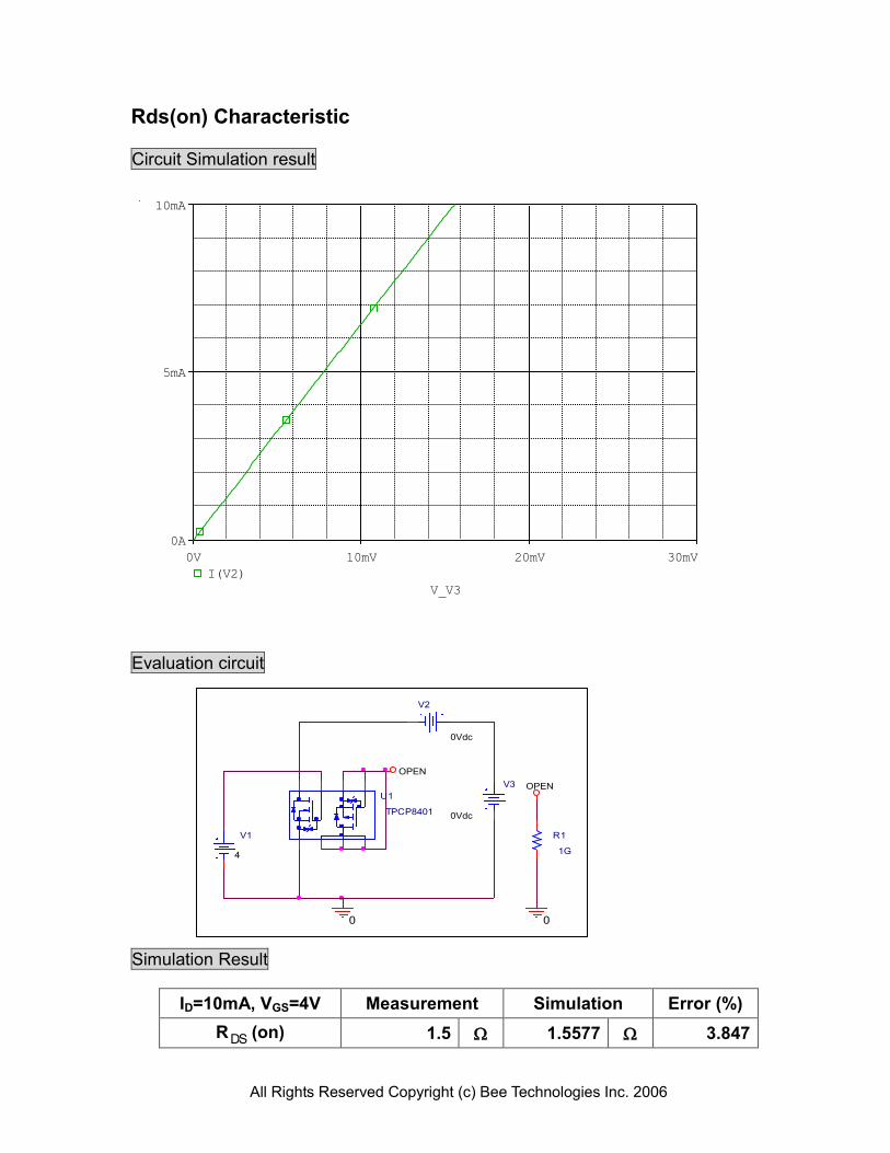
Rds(on) Characteristic
Circuit Simulation result
Evaluation circuit
Simulation Result
ID=10mA, VGS=4V Measurement Simulation Error (%)
RDS (on) 1.5 1.5577 3.847
All Rights Reserved Copyright (c) Bee Technologies Inc. 2006
U1
TPCP8401
0
OPENDbreak
D1
V1
15
I1
TD = 0
TF = 10nPW = 300uPER = 500u
I1 = 0I2 = 1m
TR = 10nOPEN
-
+W1
ION = 0IOFF = 100u
W
ROFF = 1e6RON = 1.0
I2
0.1
0
R1
1G
Time*1mA
0 0.4n 0.8n 1.2n 1.6n 2.0n
V(W1:3)
0V
1.0V
2.0V
3.0V
4.0V
5.0V
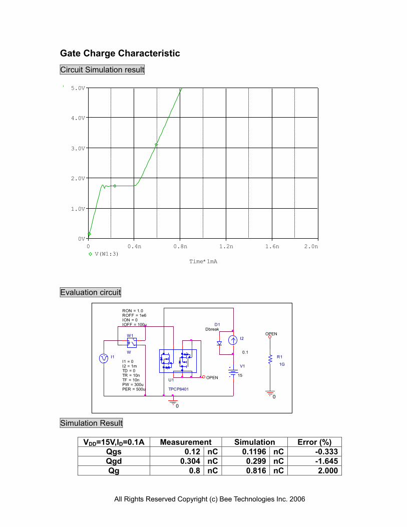
Gate Charge Characteristic
Circuit Simulation result
Evaluation circuit
Simulation Result
VDD=15V,ID=0.1A Measurement Simulation Error (%)
Qgs 0.12 nC 0.1196 nC -0.333
Qgd 0.304 nC 0.299 nC -1.645
Qg 0.8 nC 0.816 nC 2.000
All Rights Reserved Copyright (c) Bee Technologies Inc. 2006
0
1
2
3
4
5
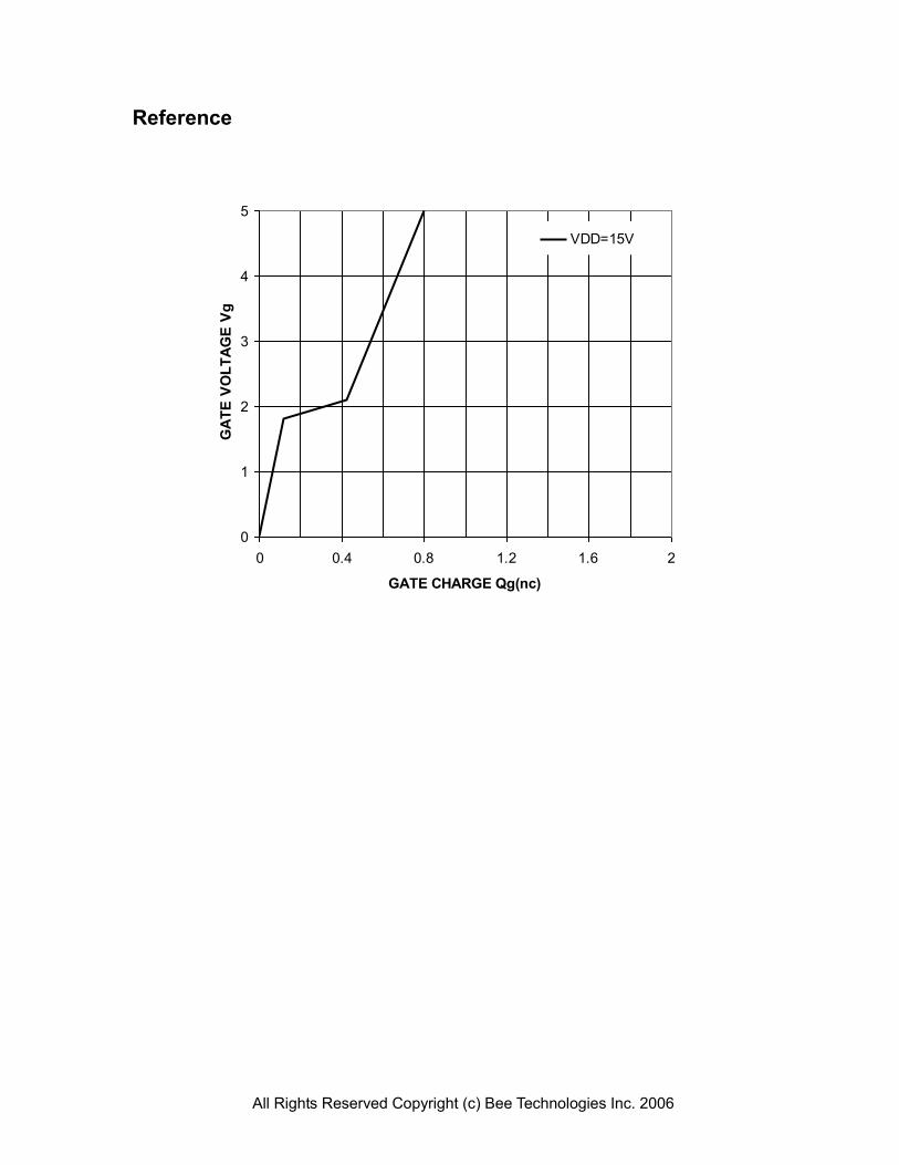
0 0.4 0.8 1.2 1.6 2
GATE CHARGE Qg(nc)
GA
TE
VO
LT
AG
E V
gVDD=15V
Reference
All Rights Reserved Copyright (c) Bee Technologies Inc. 2006
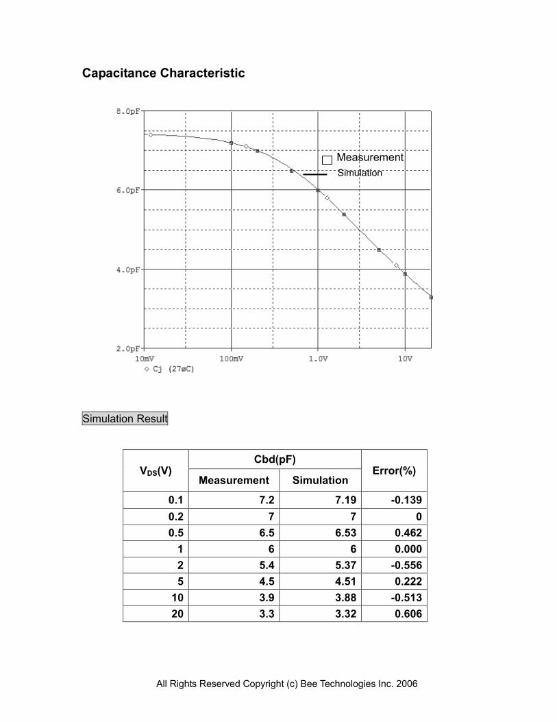
Capacitance Characteristic
Simulation Result
VDS(V) Cbd(pF)
Error(%) Measurement Simulation
0.1 7.2 7.19 -0.139
0.2 7 7 0
0.5 6.5 6.53 0.462
1 6 6 0.000
2 5.4 5.37 -0.556
5 4.5 4.51 0.222
10 3.9 3.88 -0.513
20 3.3 3.32 0.606
Simulation
Measurement
All Rights Reserved Copyright (c) Bee Technologies Inc. 2006
VOUT
0
3
0
VD3Vdc
Vsense L3
30nH
R6
1G
L4
30nHU1
TPCP8401
RL
300
VGS
OPEN
0
OPEN
R5
50
C1
100u
Time
10.000us 10.400us9.697us 10.700us
V(VOUT)/1.2 V(VGS)
0V
1.0V
2.0V
3.0V
4.0V
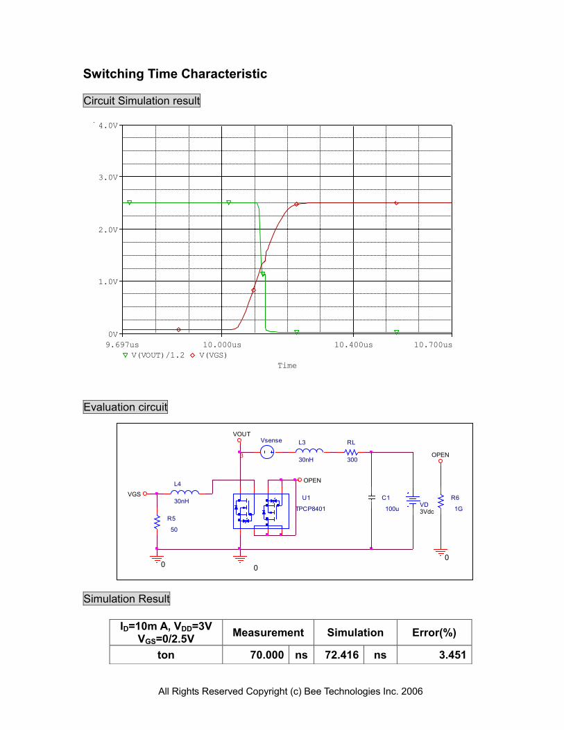
Switching Time Characteristic
Circuit Simulation result
Evaluation circuit
Simulation Result
ID=10m A, VDD=3V VGS=0/2.5V
Measurement Simulation Error(%)
ton 70.000 ns 72.416 ns 3.451
VGS
ID
All Rights Reserved Copyright (c) Bee Technologies Inc. 2006
V3
0Vdc
U1
TPCP8401
0
OPEN
0
OPEN
R1
1G
V1
1.3
V2
2
V_V2
0V 0.5V 1.0V 1.5V 2.0V
I(V3)
0A
50mA
100mA
150mA
200mA
250mA
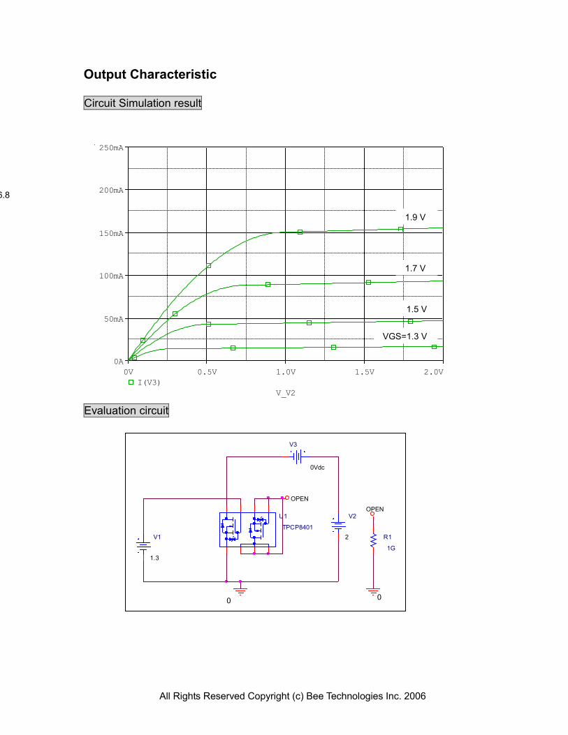
Output Characteristic
Circuit Simulation result
Evaluation circuit
VGS=1.3 V
6.8
1.5 V
1.7 V
1.9 V
All Rights Reserved Copyright (c) Bee Technologies Inc. 2006
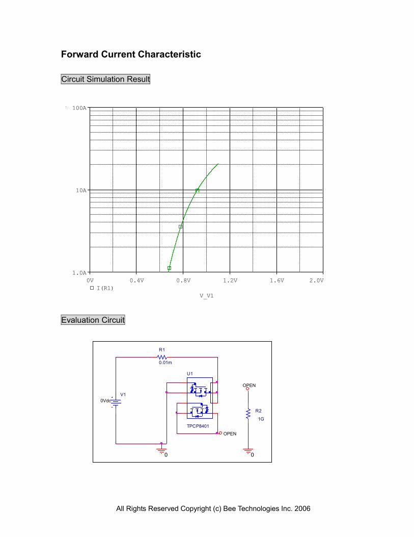
V1
0Vdc
0
OPEN
0
U1
TPCP8401
R2
1GOPEN
R1
0.01m
V_V1
0V 0.2V 0.4V 0.6V 0.8V 1.0V 1.2V 1.4V
I(R1)
0A
50mA
100mA
150mA
200mA
250mA
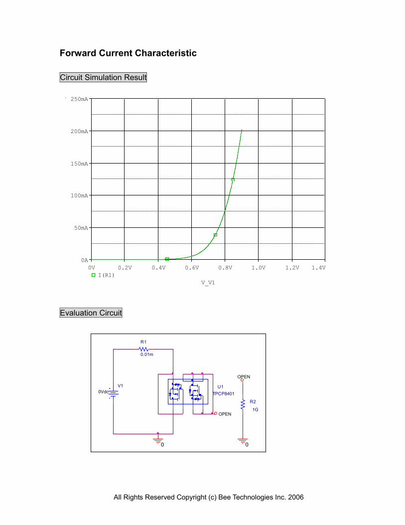
Forward Current Characteristic
Circuit Simulation Result
Evaluation Circuit
All Rights Reserved Copyright (c) Bee Technologies Inc. 2006
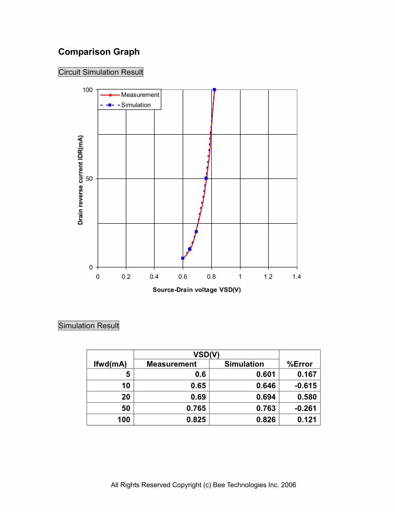
0
50
100
0 0.2 0.4 0.6 0.8 1 1.2 1.4
Source-Drain voltage VSD(V)
Dra
in r
evers
e c
urr
en
t ID
R(m
A)
Measurement
Simulation
Comparison Graph Circuit Simulation Result
Simulation Result
Ifwd(mA)
VSD(V)
%Error Measurement Simulation
5 0.6 0.601 0.167
10 0.65 0.646 -0.615
20 0.69 0.694 0.580
50 0.765 0.763 -0.261
100 0.825 0.826 0.121
All Rights Reserved Copyright (c) Bee Technologies Inc. 2006
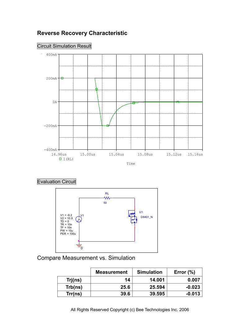
U1
D8401_NV1
TD = 0
TF = 10nPW = 15uPER = 100u
V1 = -9.2
TR = 10n
V2 = 10.9
RL
50
0
Time
14.96us 15.00us 15.04us 15.08us 15.12us 15.16us
I(RL)
-400mA
-200mA
0A
200mA
400mA
Reverse Recovery Characteristic Circuit Simulation Result
Evaluation Circuit
Compare Measurement vs. Simulation
Measurement Simulation Error (%)
Trj(ns) 14 14.001 0.007
Trb(ns) 25.6 25.594 -0.023
Trr(ns) 39.6 39.595 -0.013
All Rights Reserved Copyright (c) Bee Technologies Inc. 2006
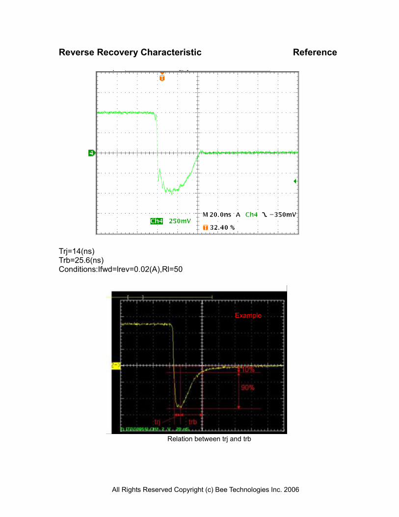
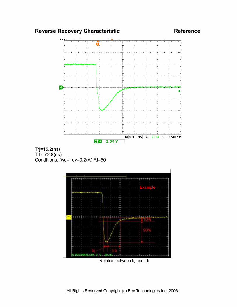
Reverse Recovery Characteristic Reference
Trj=14(ns) Trb=25.6(ns) Conditions:Ifwd=lrev=0.02(A),Rl=50
Relation between trj and trb
Example
All Rights Reserved Copyright (c) Bee Technologies Inc. 2006
R2
1G
OPEN
R1
0.01m
OPEN
0
U1
TPCP8401
R3
1G
0
V1
0Vdc
V_V1
0V 25V 50V
I(R1)
0A
5mA
10mA
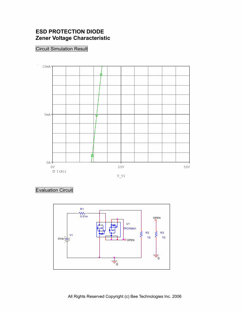
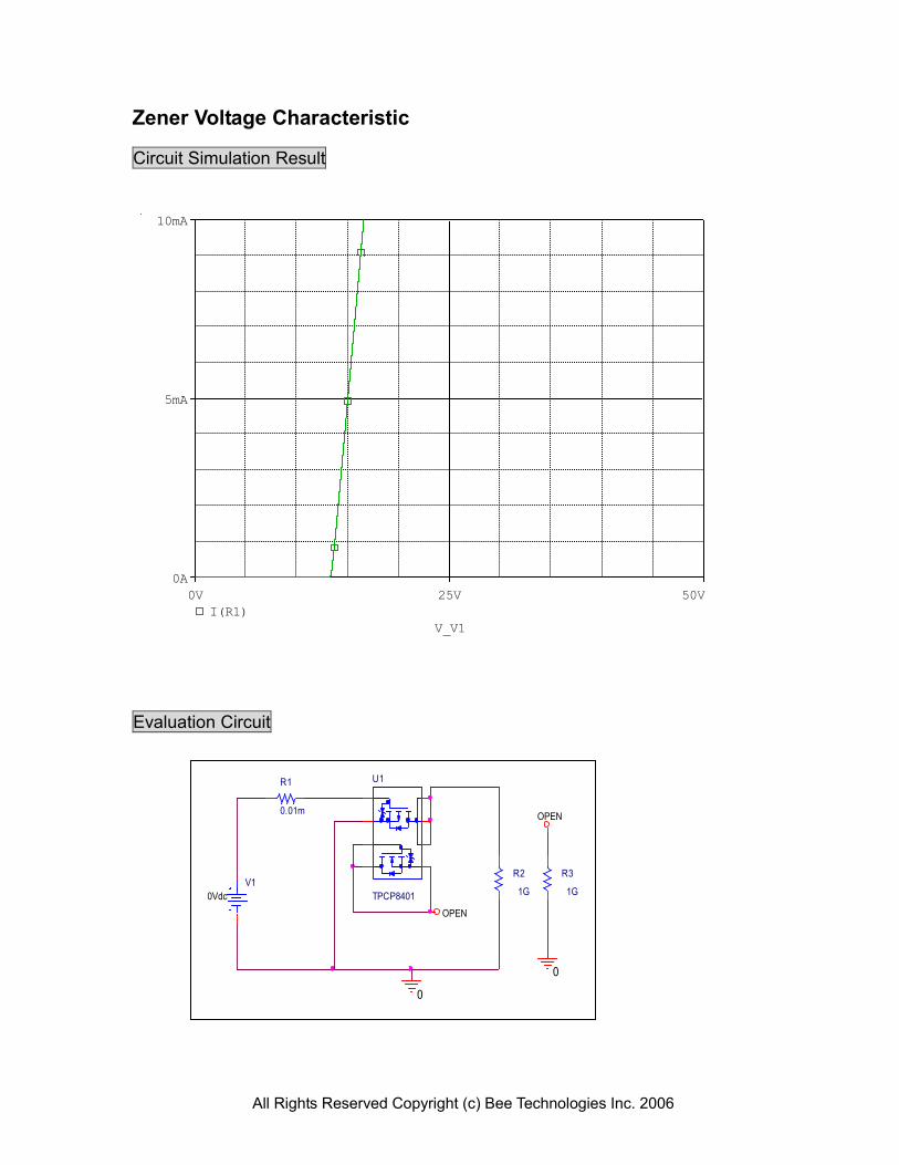
ESD PROTECTION DIODE Zener Voltage Characteristic
Circuit Simulation Result
Evaluation Circuit
All Rights Reserved Copyright (c) Bee Technologies Inc. 2006
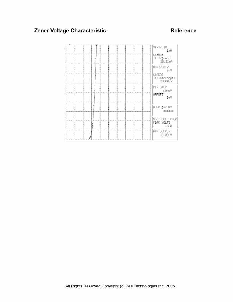
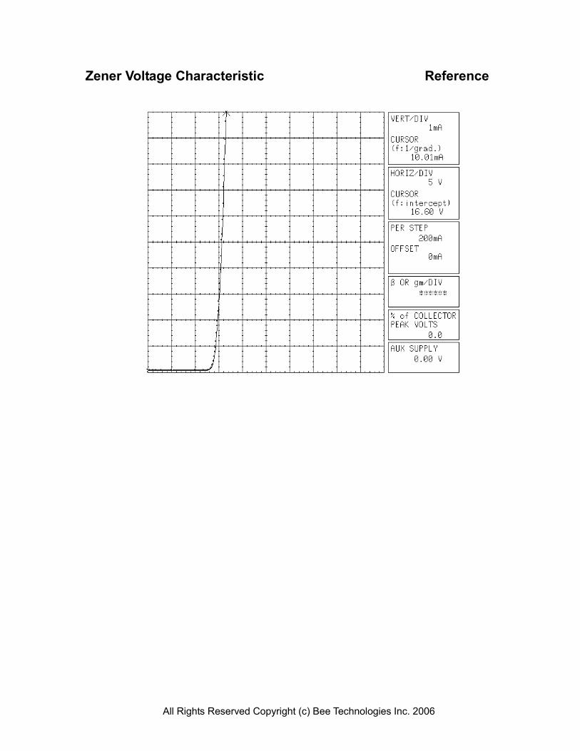
Zener Voltage Characteristic Reference
All Rights Reserved Copyright (c) Bee Technologies Inc. 2006
2.5
3.5
4.5
5.5
6.5
7.5
8.5
9.5
0 0.4 0.8 1.2 1.6 2
ID(A)
gfs
Measurement
Simulation
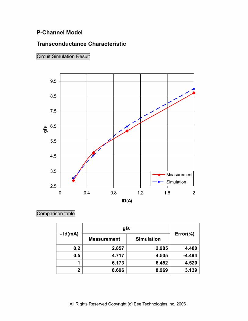
P-Channel Model
Transconductance Characteristic
Circuit Simulation Result
Comparison table
- Id(mA) gfs
Error(%) Measurement Simulation
0.2 2.857 2.985 4.480
0.5 4.717 4.505 -4.494
1 6.173 6.452 4.520
2 8.696 8.969 3.139
All Rights Reserved Copyright (c) Bee Technologies Inc. 2006
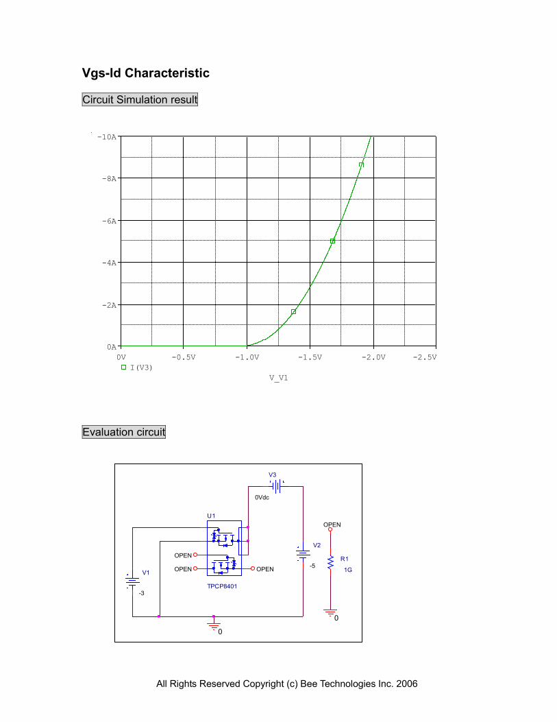
OPENOPEN
U1
TPCP8401
V2
-5R1
1G
OPEN
0
OPEN
0
V3
0Vdc
V1
-3
V_V1
0V -0.5V -1.0V -1.5V -2.0V -2.5V
I(V3)
0A
-2A
-4A
-6A
-8A
-10A
Vgs-Id Characteristic
Circuit Simulation result
Evaluation circuit
All Rights Reserved Copyright (c) Bee Technologies Inc. 2006
0.2
0.6
1
1.4
1.8
0 1 2 3
VGS - Gate to Source Voltage - V
ID -
Dra
in C
urr
en
t (A
)
Measurement
Simulation
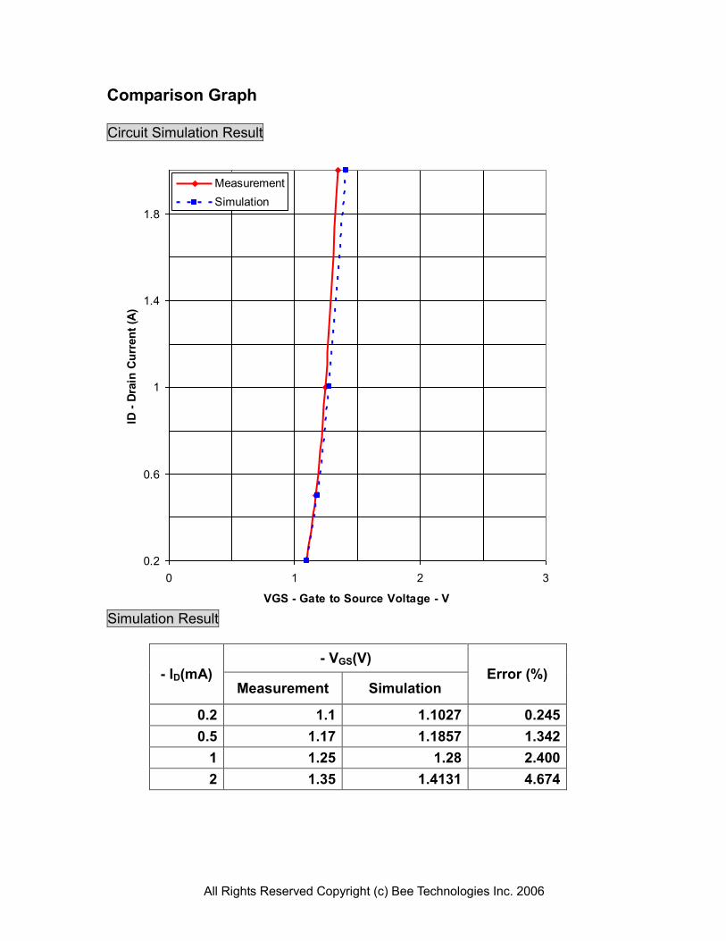
Comparison Graph Circuit Simulation Result
Simulation Result
- ID(mA) - VGS(V)
Error (%) Measurement Simulation
0.2 1.1 1.1027 0.245
0.5 1.17 1.1857 1.342
1 1.25 1.28 2.400
2 1.35 1.4131 4.674
All Rights Reserved Copyright (c) Bee Technologies Inc. 2006
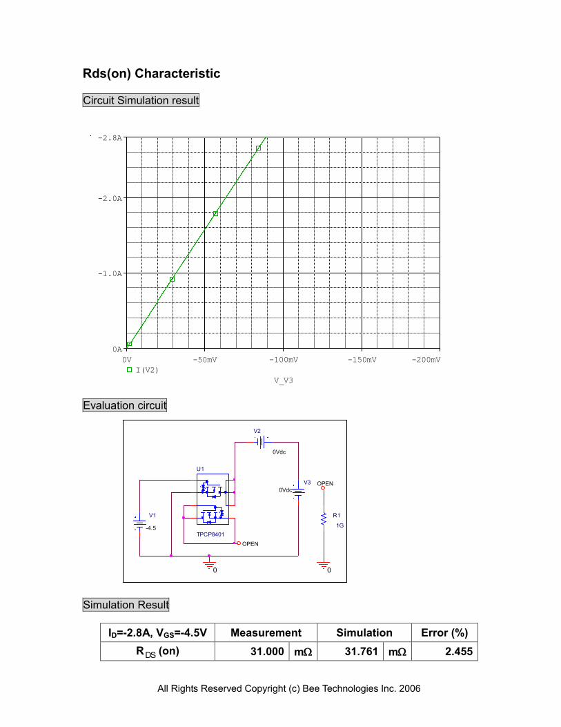
V1
-4.5
0
V2
0Vdc
OPEN
OPEN
V3
0Vdc
R1
1G
0
U1
TPCP8401
V_V3
0V -50mV -100mV -150mV -200mV
I(V2)
0A
-1.0A
-2.0A
-2.8A
Rds(on) Characteristic
Circuit Simulation result
Evaluation circuit
Simulation Result
ID=-2.8A, VGS=-4.5V Measurement Simulation Error (%)
RDS (on) 31.000 m 31.761 m 2.455
All Rights Reserved Copyright (c) Bee Technologies Inc. 2006
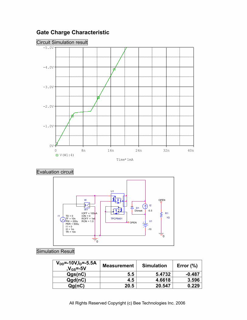
I2
-5.5
U1
TPCP8401
-
+
W1
ION = 0IOFF = 100uA
W
ROFF = 1e6RON = 1.0
OPEN
I1 TD = 0TF = 10nPW = 200uPER = 500uI1 = 0I2 = 1mTR = 10n
0
0
V1
-10
OPEN
R1
1G
DbreakD1
Time*1mA
0 8n 16n 24n 32n 40n
V(W1:4)
0V
-1.0V
-2.0V
-3.0V
-4.0V
-5.0V
Gate Charge Characteristic
Circuit Simulation result
Evaluation circuit
Simulation Result
VDD=-10V,ID=-5.5A ,VGS=-5V
Measurement Simulation Error (%)
Qgs(nC) 5.5 5.4732 -0.487
Qgd(nC) 4.5 4.6618 3.596
Qg(nC) 20.5 20.547 0.229
All Rights Reserved Copyright (c) Bee Technologies Inc. 2006
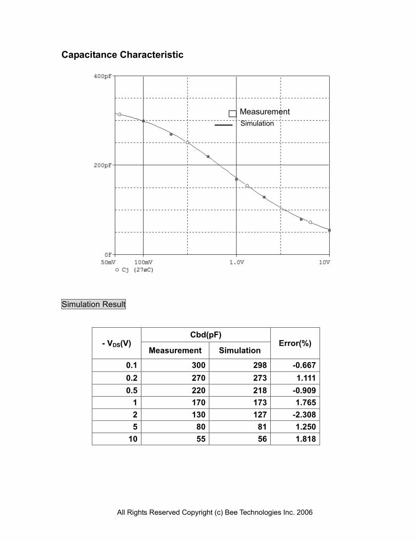
Capacitance Characteristic
Simulation Result
- VDS(V) Cbd(pF)
Error(%) Measurement Simulation
0.1 300 298 -0.667
0.2 270 273 1.111
0.5 220 218 -0.909
1 170 173 1.765
2 130 127 -2.308
5 80 81 1.250
10 55 56 1.818
Simulation
Measurement
All Rights Reserved Copyright (c) Bee Technologies Inc. 2006
0
V2
TD = 2u
TF = 4nPW = 10uPER = 30u
V1 = 0
TR = 4n
V2 = -5
OPEN
R1
1G
L2
30nH
R2
2.1
0
R4
4.7
L1
50nH
U1
TPCP8401
OPEN
V1
-6
Time
1.9us 2.0us 2.1us 2.2us
V(U1:5) V(U1:2)/1.2
0V
-2V
-4V
-6V
-8V
-10V
Switching Time Characteristic
Circuit Simulation result
Evaluation circuit
Simulation Result
ID=-2.8 A, VDD=-6V VGS=0/-5V
Measurement Simulation Error(%)
Ton(ns) 16 16.039 0.244
VGS
ID
All Rights Reserved Copyright (c) Bee Technologies Inc. 2006
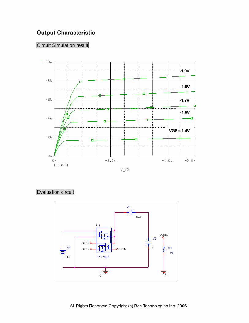
OPEN
0
OPEN
OPEN
OPEN
R1
1G
0
V3
0Vdc
V2
-5V1
-1.4
U1
TPCP8401
V_V2
0V -2.0V -4.0V -5.0V
I(V3)
0A
-2A
-4A
-6A
-8A
-10A
Output Characteristic
Circuit Simulation result
Evaluation circuit
VGS=-1.4V
-1.6V
-1.7V
-1.8V
-1.9V
All Rights Reserved Copyright (c) Bee Technologies Inc. 2006
U1
TPCP8401
OPEN
0
R1
0.01m
R2
1G
0
V1
0Vdc
OPEN
V_V1
0V 0.4V 0.8V 1.2V 1.6V 2.0V
I(R1)
1.0A
10A
100A
Forward Current Characteristic
Circuit Simulation Result
Evaluation Circuit
All Rights Reserved Copyright (c) Bee Technologies Inc. 2006
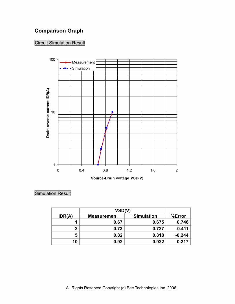
1
10
100
0 0.4 0.8 1.2 1.6 2
Source-Drain voltage VSD(V)
Dra
in r
evers
e c
urr
en
t ID
R(A
)
Measurement
Simulation
Comparison Graph Circuit Simulation Result
Simulation Result
IDR(A)
VSD(V)
%Error Measuremen Simulation
1 0.67 0.675 0.746
2 0.73 0.727 -0.411
5 0.82 0.818 -0.244
10 0.92 0.922 0.217
All Rights Reserved Copyright (c) Bee Technologies Inc. 2006
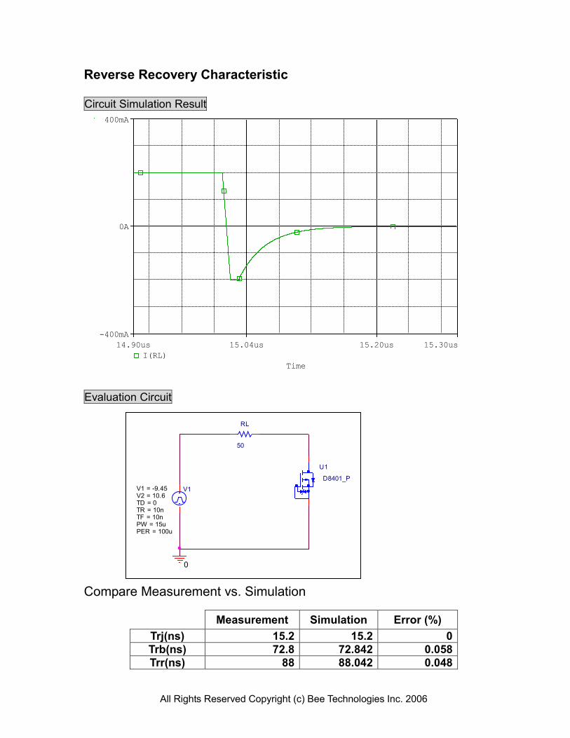
0
U1
D8401_P
V1
TD = 0
TF = 10nPW = 15uPER = 100u
V1 = -9.45
TR = 10n
V2 = 10.6
RL
50
Time
15.04us 15.20us14.90us 15.30us
I(RL)
-400mA
0A
400mA
Reverse Recovery Characteristic Circuit Simulation Result
Evaluation Circuit Compare Measurement vs. Simulation
Measurement Simulation Error (%)
Trj(ns) 15.2 15.2 0
Trb(ns) 72.8 72.842 0.058
Trr(ns) 88 88.042 0.048
All Rights Reserved Copyright (c) Bee Technologies Inc. 2006
Reverse Recovery Characteristic Reference
Trj=15.2(ns) Trb=72.8(ns) Conditions:Ifwd=lrev=0.2(A),Rl=50
Relation between trj and trb
Example
All Rights Reserved Copyright (c) Bee Technologies Inc. 2006
R2
1G
OPEN
0
U1
TPCP8401
R3
1G
OPEN
R1
0.01m
0
V1
0Vdc
V_V1
0V 25V 50V
I(R1)
0A
5mA
10mA
Zener Voltage Characteristic
Circuit Simulation Result
Evaluation Circuit
All Rights Reserved Copyright (c) Bee Technologies Inc. 2006
Zener Voltage Characteristic Reference