solar cell/module degradation and failure...
TRANSCRIPT

SOLAR CELL/MODULE
DEGRADATION
AND FAILURE DIAGNOSTICS
T.J. McMahon
National Renewable Energy Lab
Golden, CO USA

2
Purpose
• Review of solar cell/module degradation
and failure diagnostic tools.
• Coring technique to acquire samples and
evaluate interface toughness.
• Accelerated testing and failure
mechanisms in PV.

3
Outline
• Basic Module Types
• Diagnostics
• Distributed vs localised
• Definition of reliability
• Accelerated testing in PV
• Failure mechanisms
• Summary
4
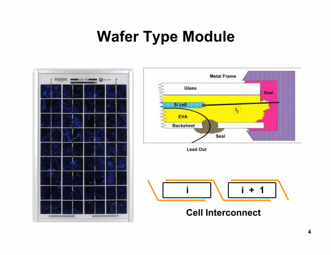
Wafer Type Module
Cell Interconnect
i i + 1
5
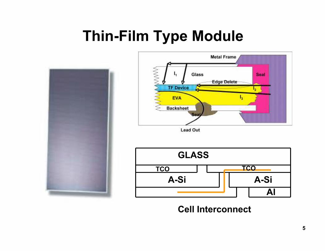
Thin-Film Type Module
Cell Interconnect
A-Si A-Si
GLASS
Al
TCO TCO
6
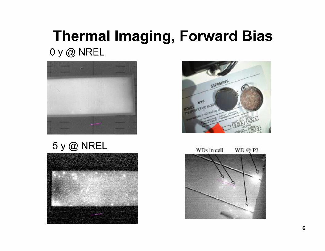
Thermal Imaging, Forward Bias
5 y @ NREL
0 y @ NREL

7
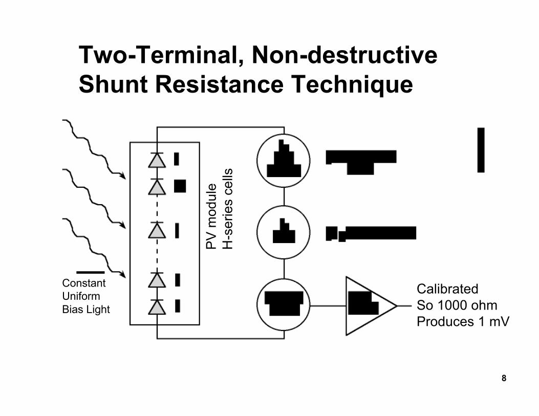
Two-Terminal, Non-destructive
Shunt Resistance Technique
5 y @ NREL 7 y @ NREL
Cells 1 thru 48 Cells 1 thru 48
R (
oh
ms/C
ell)
R (
oh
ms/C
ell)
0 0
25 25
8
Two-Terminal, Non-destructive
Shunt Resistance Technique
Constant
Uniform
Bias Light
Calibrated
So 1000 ohm
Produces 1 mV
PV
mo
du
le
H-s
eri
es c
ells
9
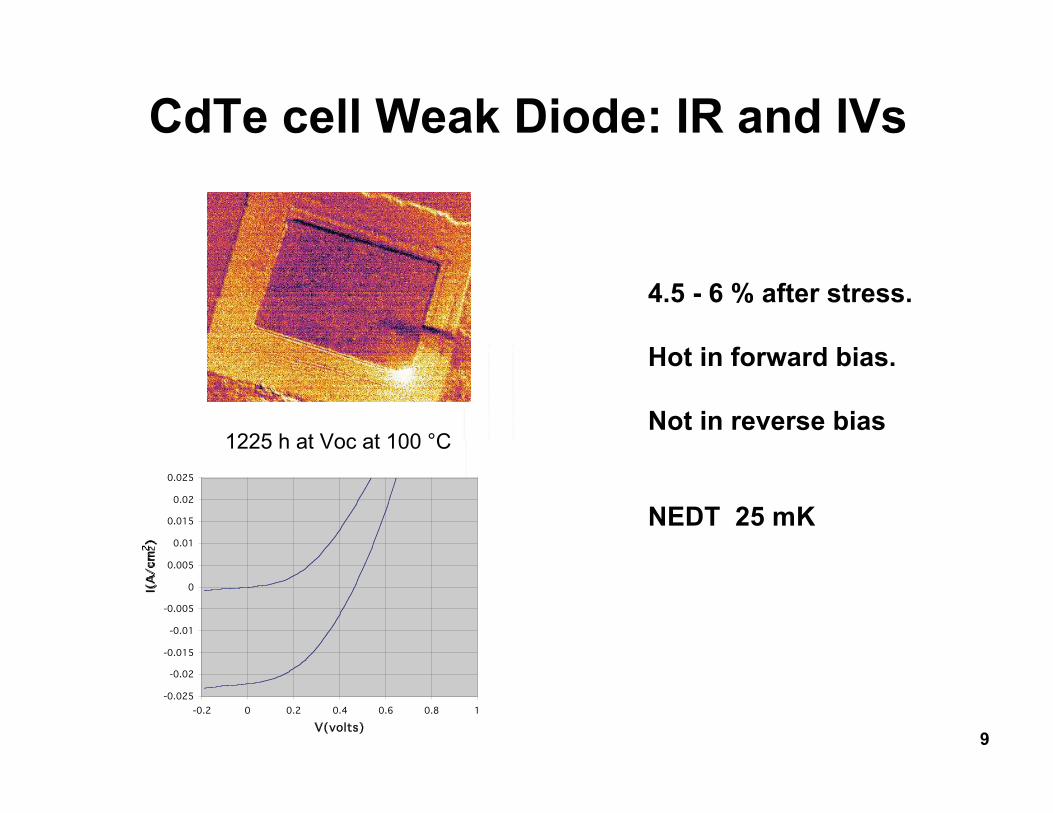
CdTe cell Weak Diode: IR and IVs
-0.025
-0.02
-0.015
-0.01
-0.005
0
0.005
0.01
0.015
0.02
0.025
-0.2 0 0.2 0.4 0.6 0.8 1
V(volts)
I(A/cm
2)
4.5 - 6 % after stress.
Hot in forward bias.
Not in reverse bias
NEDT 25 mK
1225 h at Voc at 100 °C
10
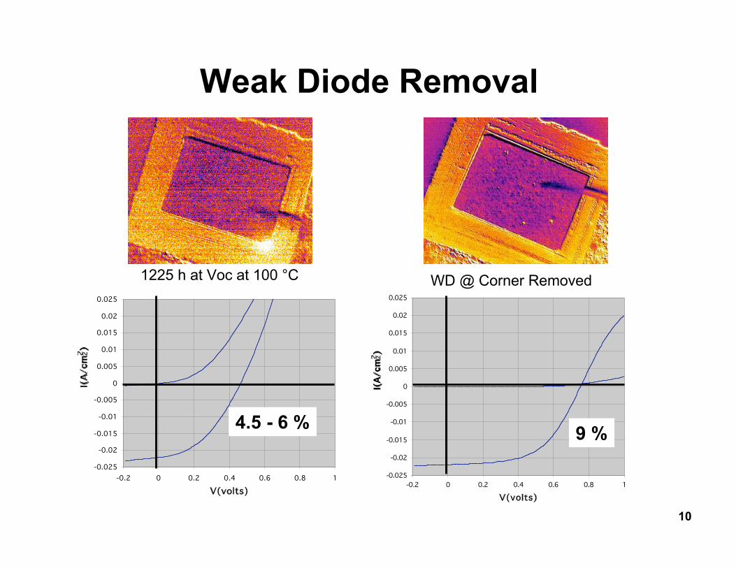
Weak Diode Removal
4.5 - 6 %
-0.025
-0.02
-0.015
-0.01
-0.005
0
0.005
0.01
0.015
0.02
0.025
-0.2 0 0.2 0.4 0.6 0.8 1
V(volts)
I(A/cm
2)
-0.025
-0.02
-0.015
-0.01
-0.005
0
0.005
0.01
0.015
0.02
0.025
-0.2 0 0.2 0.4 0.6 0.8 1
V(volts)
I(A/cm
2)
4.5 - 6 %9 %
1225 h at Voc at 100 °C WD @ Corner Removed

11
P-Spice circuit w/WD
-0.025
-0.02
-0.015
-0.01
-0.005
0
0.005
0.01
0.015
0.02
0.025
-0.2 0 0.2 0.4 0.6 0.8 1
V(volts)
I(A/cm
2)
4.5 - 6 %
12
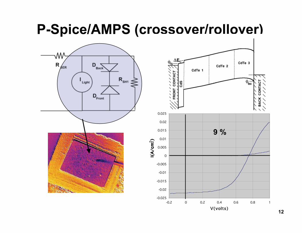
P-Spice/AMPS (crossover/rollover)
-0.025
-0.02
-0.015
-0.01
-0.005
0
0.005
0.01
0.015
0.02
0.025
-0.2 0 0.2 0.4 0.6 0.8 1
V(volts)
I(A/cm
2)
9 %
13
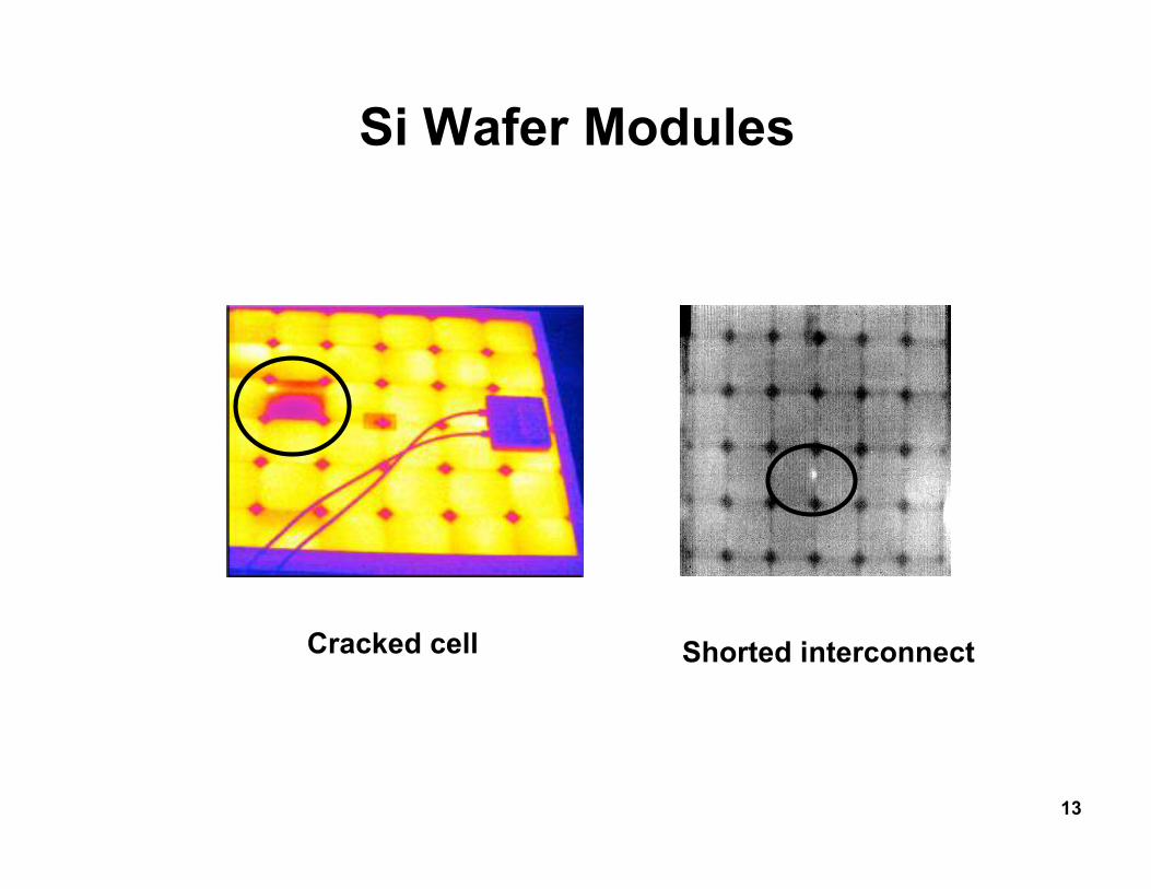
Si Wafer Modules
Cracked cell Shorted interconnect

14
Shear Strength Measurement at
Front Cell/EVA Interface
Tempered Front Glass
EVA
Si Cell
EVA
TPE Backsheet
Tempered Front Glass
EVA
Si Cell
15
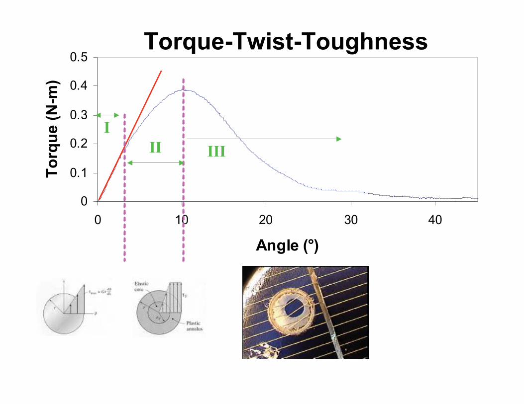
0
0.1
0.2
0.3
0.4
0.5
0 10 20 30 40
Angle (°)
To
rqu
e (
N-m
)
I
II III
555555555555555555555555555555555555555555555
Torque-Twist-Toughness
16
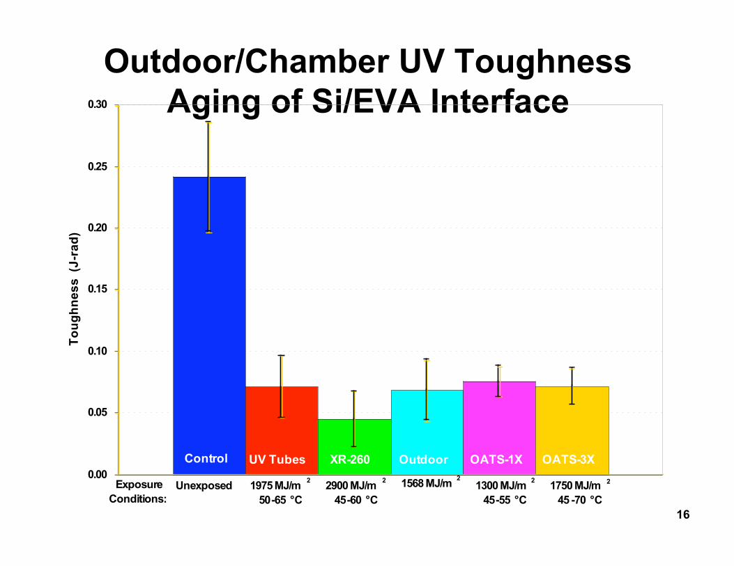
Outdoor/Chamber UV Toughness
Aging of Si/EVA Interface
0.00
0.05
0.10
0.15
0.20
0.25
0.30
To
ug
hn
es
s (J
-ra
d)
Control UV Tubes XR-260 Outdoor OATS-1X OATS-3X
1975 MJ/m2
50-65 °C
2900 MJ/m2
45-60 °C
1568 MJ/m2
1300 MJ/m2
45-55 °C
1750 MJ/m2
45 -70 °C
UnexposedExposure
Conditions:

17
Failure Mechanisms (FMs)
• Packaging vs Cell
– Packaging is 90% of the field returns * ^
– 50% of the cost
• Distributed vs Localised
• General vs Technology Specific
* Includes cell interconnects.
^ Failure rate and cause depend on how mature the
technology is, e.g. BP Silicon is 1/4200 module year;
Newbee modules are 1/10 - 1/100.

18
Service Life Prediction

19
FMs: Modules GeneralField returns and anticipated failures
• Front Sheet/Encap failure
• Cell/Encap failure
• Back Sheet/Encap failure
• Stress breakage of glass/glass laminate
• Glass edge damage/breakage
• Corrosion of grid lines / ohmic contact / R series
• Poor solder joint(string ribbons and J-boxes)
• By-pass diode failure
• Frame/mounting failure
• Failure of electrical safety/Hi-Pot isolation

20
FMs: Modules Technology Specific
Field returns and anticipated failures
Wafer Si:• Crack formation in thinner cells
• Solder joint degradation on cells
• Ribbon related open circuit or shunting
Thin Film:• Flexible packaging interconnect failure
• Laser scribe interconnect failure
• De-adhesion of device layers, inc. CTOs and metal contacts
• Busbar adhesion and electrical contact
• Weak diode or shunt defects
• Decreasing ff (E-field collection or series resistance issues)
• Moisture ingress problems, esp. flexible with CIS
• Diffusion, esp. Cu in CdTe
• Staebler-Wronski, esp. single junction a-Si
• SnO2 corrosion in superstrate cells
21
Conclusions
• Artificially accelerating environmental stress on
PV cells and modules is used to test for their
reliability under field conditions.
• Failure diagnostic techniques are used to
locate, identify, and evaluate resulting failure
modes.
• A new core torque-twist technique used to
evaluate module packaging durability and
obtain sample specimens for failure analysis is
reviewed.
• Proposed failure mechanisms for the different
module technologies.