snosa03g –november 2002–revised december 2014 … · lmh6702 snosa03g –november...
TRANSCRIPT
1M 10M 100M 1G
Frequency (Hz)
-7
-6
-5
-4
-3
-2
-1
0
1
Gai
n (d
B)
-430
-380
-330
-280
-230
-180
-130
-80
-30
Pha
se (
°)
AV = -1
AV = -10
AV = -4
AV = -2
PHASE
GAIN
1M 10M 100MFrequency (Hz)
-105
-100
-95-90
-85
-80
-75
-70
-65
-60
-40
HD
(dB
c)
-55
-50-45
HD2, RL = 1 k:
HD3, RL = 1 k:
HD2, RL = 100 :
HD3, RL = 100 :
Product
Folder
Sample &Buy
Technical
Documents
Tools &
Software
Support &Community
LMH6702SNOSA03G –NOVEMBER 2002–REVISED DECEMBER 2014
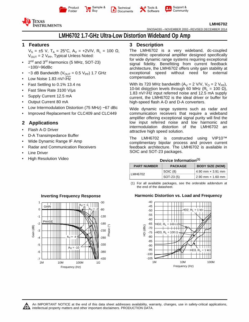
LMH6702 1.7-GHz Ultra-Low Distortion Wideband Op Amp1 Features 3 Description
The LMH6702 is a very wideband, dc-coupled1VS = ±5 V, TA = 25°C, AV = +2V/V, RL = 100 Ω,monolithic operational amplifier designed specificallyVOUT = 2 VPP, Typical Unless Noted:for wide dynamic range systems requiring exceptional
• 2nd and 3rd Harmonics (5 MHz, SOT-23) signal fidelity. Benefitting from current feedback−100/−96dBc architecture, the LMH6702 offers unity gain stability at
exceptional speed without need for external• −3 dB Bandwidth (VOUT = 0.5 VPP) 1.7 GHzcompensation.• Low Noise 1.83 nV/√HzWith its 720 MHz bandwidth (AV = 2 V/V, VO = 2 VPP),• Fast Settling to 0.1% 13.4 ns10-bit distortion levels through 60 MHz (RL = 100 Ω),• Fast Slew Rate 3100 V/μs1.83 nV/√Hz input referred noise and 12.5 mA supply
• Supply Current 12.5 mA current, the LMH6702 is the ideal driver or buffer for• Output Current 80 mA high-speed flash A-D and D-A converters.• Low Intermodulation Distortion (75 MHz) −67 dBc Wide dynamic range systems such as radar and• Improved Replacement for CLC409 and CLC449 communication receivers that require a wideband
amplifier offering exceptional signal purity will find thelow input referred noise and low harmonic and2 Applicationsintermodulation distortion of the LMH6702 an
• Flash A-D Driver attractive high speed solution.• D-A Transimpedance Buffer The LMH6702 is constructed using VIP10™• Wide Dynamic Range IF Amp complimentary bipolar process and proven current• Radar and Communication Receivers feedback architecture. The LMH6702 is available in
SOIC and SOT-23 packages.• Line Driver• High Resolution Video Device Information(1)
PART NUMBER PACKAGE BODY SIZE (NOM)SOIC (8) 4.90 mm × 3.91 mm
LMH6702SOT-23 (5) 2.90 mm × 1.60 mm
(1) For all available packages, see the orderable addendum atthe end of the datasheet.
Harmonic Distortion vs. Load and FrequencyInverting Frequency Response
1
An IMPORTANT NOTICE at the end of this data sheet addresses availability, warranty, changes, use in safety-critical applications,intellectual property matters and other important disclaimers. PRODUCTION DATA.
LMH6702SNOSA03G –NOVEMBER 2002–REVISED DECEMBER 2014 www.ti.com
Table of Contents7.3 Device Functional Modes........................................ 121 Features .................................................................. 1
8 Application and Implementation ........................ 132 Applications ........................................................... 18.1 Application Information............................................ 133 Description ............................................................. 18.2 Typical Application ................................................. 134 Revision History..................................................... 2
9 Power Supply Recommendations ...................... 155 Pin Configuration and Functions ......................... 310 Layout................................................................... 156 Specifications......................................................... 4
10.1 Layout Guidelines ................................................. 156.1 Absolute Maximum Ratings ...................................... 410.2 Layout Example .................................................... 166.2 ESD Ratings.............................................................. 4
11 Device and Documentation Support ................. 176.3 Recommended Operating Conditions....................... 411.1 Documentation Support ....................................... 176.4 Thermal Information .................................................. 411.2 Trademarks ........................................................... 176.5 Electrical Characteristics........................................... 511.3 Electrostatic Discharge Caution............................ 176.6 Typical Performance Characteristics ........................ 711.4 Glossary ................................................................ 177 Detailed Description ............................................ 11
12 Mechanical, Packaging, and Orderable7.1 Overview ................................................................. 11Information ........................................................... 177.2 Feature Description................................................. 11
4 Revision HistoryNOTE: Page numbers for previous revisions may differ from page numbers in the current version.
Changes from Revision F (March 2013) to Revision G Page
• Added, updated, or renamed the following sections: Device Information Table, Specifications; Application andImplementation; Power Supply Recommendations; Layout; Device and Documentation Support; Mechanical,Packaging, and Ordering Information .................................................................................................................................... 1
• Changed ±5 to ±4 in Recommended Operating Conditions table.......................................................................................... 4
Changes from Revision E (March 2013) to Revision F Page
• Changed layout of National Data Sheet to TI format ............................................................................................................. 1
2 Submit Documentation Feedback Copyright © 2002–2014, Texas Instruments Incorporated
Product Folder Links: LMH6702
V+
1
2
3
4 5
6
7
8N/C
-IN
+IN
V-
N/C
OUT
N/C
-
+
OUT
V-
+IN
V+
-IN
+ -
1
2
3
5
4
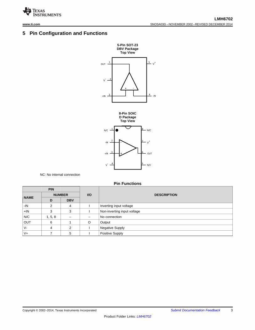
LMH6702www.ti.com SNOSA03G –NOVEMBER 2002–REVISED DECEMBER 2014
5 Pin Configuration and Functions
5-Pin SOT-23DBV Package
Top View
8-Pin SOICD PackageTop View
NC: No internal connection
Pin FunctionsPIN
NUMBER I/O DESCRIPTIONNAME
D DBV-IN 2 4 I Inverting input voltage+IN 3 3 I Non-inverting input voltageN/C 1, 5, 8 – – No connectionOUT 6 1 O OutputV- 4 2 I Negative SupplyV+ 7 5 I Positive Supply
Copyright © 2002–2014, Texas Instruments Incorporated Submit Documentation Feedback 3
Product Folder Links: LMH6702
LMH6702SNOSA03G –NOVEMBER 2002–REVISED DECEMBER 2014 www.ti.com
6 Specifications
6.1 Absolute Maximum Ratingsover operating free-air temperature range (unless otherwise noted) (1) (2)
MIN MAX UNITVS ±6.75 VIOUT See (3)
Common mode input voltage V− to V+ VMaximum junction temperature 150 °CStorage temperature −65 150 °C
Infrared or convection (20 s) 235 °CSoldering information
Wave soldering (10 s) 260 °C
(1) Absolute Maximum Ratings indicate limits beyond which damage to the device may occur. Operating Ratings indicate conditions forwhich the device is intended to be functional, but specific performance is not ensured. For ensured specifications, see the ElectricalCharacteristics tables.
(2) If Military/Aerospace specified devices are required, please contact the TI Sales Office/ Distributors for availability and specifications.(3) The maximum output current (IOUT) is determined by device power dissipation limitations.
6.2 ESD RatingsVALUE UNIT
Human-body model (HBM), per ANSI/ESDA/JEDEC JS-001 (1) ±2000V(ESD) Electrostatic discharge V
Machine Model (MM), per JEDEC specification JESD22-C101, all pins (2) ±200
(1) Human body model: 1.5 kΩ in series with 100 pF. JEDEC document JEP155 states that 2000-V HBM allows safe manufacturing with astandard ESD control process. Manufacturing with less than 2000-V HBM is possible with the necessary precautions. Pins listed as±2000 V may actually have higher performance.
(2) Machine model: 0 Ω in series with 200 pF. JEDEC document JEP157 states that 200-V MM allows safe manufacturing with a standardESD control process. Manufacturing with less than 200-V MM is possible with the necessary precautions. Pins listed as ±200 V mayactually have higher performance.
6.3 Recommended Operating Conditionsover operating free-air temperature range (unless otherwise noted) (1)
PARAMETER MIN MAX UNITOperating temperature −40 +85 °CNominal supply voltage ±4 ±6 V
(1) Absolute Maximum Ratings indicate limits beyond which damage to the device may occur. Operating Ratings indicate conditions forwhich the device is intended to be functional, but specific performance is not ensured. For ensured specifications, see the ElectricalCharacteristics tables.
6.4 Thermal InformationDBV D
THERMAL METRIC (1) UNIT5 PINS 8 PINS
RθJA Junction-to-ambient thermal resistance 187 160°C/W
RθJC(top) Junction-to-case (top) thermal resistance 120 75
(1) For more information about traditional and new thermal metrics, see the IC Package Thermal Metrics application report, SPRA953.
4 Submit Documentation Feedback Copyright © 2002–2014, Texas Instruments Incorporated
Product Folder Links: LMH6702
LMH6702www.ti.com SNOSA03G –NOVEMBER 2002–REVISED DECEMBER 2014
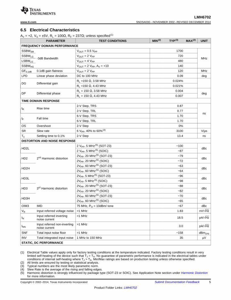
6.5 Electrical CharacteristicsAV = +2, VS = ±5V, RL = 100Ω, RF = 237Ω; unless specified (1)
PARAMETER TEST CONDITIONS MIN (2) TYP (3) MAX (2) UNITFREQUENCY DOMAIN PERFORMANCESSBWSM VOUT = 0.5 VPP 1700SSBWLG VOUT = 2 VPP 720
-3dB Bandwidth MHzLSBWLG VOUT = 4 VPP 480SSBWHG VOUT = 2 VPP, AV = +10 140GF0.1dB 0.1dB gain flatness VOUT = 2 VPP 120 MHzLPD Linear phase deviation DC to 100 MHz 0.09 deg
RL =150 Ω, 3.58 MHz 0.024%DG Differential gain
RL =150 Ω, 4.43 MHz 0.021%RL = 150 Ω, 3.58 MHz 0.004
DP Differential phase degRL = 150 Ω, 4.43 MHz 0.007
TIME DOMAIN RESPONSE2-V Step, TRS 0.87
tR Rise time2-V Step, TRL 0.77
ns6-V Step, TRS 1.70
tF Fall time6-V Step, TRL 1.70
OS Overshoot 2-V Step 0%SR Slew rate 6 VPP, 40% to 60% (4) 3100 V/µsTs Settling time to 0.1% 2-V Step 13.4 nsDISTORTION AND NOISE RESPONSE
2 VPP, 5 MHz (5) (SOT-23) −100HD2L dBc
2 VPP, 5 MHz (5) (SOIC) −872VPP, 20 MHz (5) (SOT-23) −79
HD2 2nd Harmonic distortion dBc2VPP, 20 MHz (5) (SOIC) −722VPP, 60 MHz (5) (SOT-23) −63
HD2H dBc2VPP, 60 MHz (5) (SOIC) −642VPP, 5 MHz (5) (SOT-23) −96
HD3L dBc2VPP, 5 MHz (5) (SOIC) −982VPP, 20 MHz (5) (SOT-23) −88
HD3 3rd Harmonic distortion dBc2VPP, 20 MHz (5) (SOIC) −822VPP, 60 MHz (5) (SOT-23) −70
HD3H dBc2VPP, 60 MHz (5) (SOIC) −65
OIM3 IMD 75 MHz, PO = 10dBm/ tone −67 dBcVN Input referred voltage noise >1 MHz 1.83 nV/√Hz
Input referred inverting >1 MHzIN 18.5 pA/√Hznoise currentInput referred non-inverting >1 MHzINN 3.0 pA/√Hznoise current
SNF Total input noise floor >1 MHz −158 dBm1Hz
INV Total integrated input noise 1 MHz to 150 MHz 35 µVSTATIC, DC PERFORMANCE
(1) Electrical Table values apply only for factory testing conditions at the temperature indicated. Factory testing conditions result in verylimited self-heating of the device such that TJ = TA. No guarantee of parametric performance is indicated in the electrical tables underconditions of internal self-heating where TJ > TA. Min/Max ratings are based on production testing unless otherwise specified.
(2) All limits are ensured by testing or statistical analysis.(3) Typical numbers are the most likely parametric norm.(4) Slew Rate is the average of the rising and falling edges.(5) Harmonic distortion is strongly influenced by package type (SOT-23 or SOIC). See Application Note section under Harmonic Distortion
for more information.
Copyright © 2002–2014, Texas Instruments Incorporated Submit Documentation Feedback 5
Product Folder Links: LMH6702

LMH6702SNOSA03G –NOVEMBER 2002–REVISED DECEMBER 2014 www.ti.com
Electrical Characteristics (continued)AV = +2, VS = ±5V, RL = 100Ω, RF = 237Ω; unless specified(1)
PARAMETER TEST CONDITIONS MIN (2) TYP (3) MAX (2) UNIT±1.0 ±4.5
VIO Input offset voltage mV-40 ≤ TJ ≤ 85 ±6.0
Input offset voltage averageDVIO See (6) −13 µV/°Cdrift−6 ±15
IBN Input bias current Non-Inverting (7) µA-40 ≤ TJ ≤ 85 ±21
Input bias current averageDIBN Non-Inverting (6) +40 nA/°Cdrift−8 ±30
IBI Input bias current Inverting (7) µA-40 ≤ TJ ≤ 85 ±34
Input bias current averageDIBI Inverting (6) −10 nA/°Cdrift47 52
PSRR Power supply rejection ratio DC dB-40 ≤ TJ ≤ 85 45
45 48Common mode rejectionCMRR DC dBration -40 ≤ TJ ≤ 85 44RL = ∞ 11.0 12.5 16.1
ICC Supply current mA-40 ≤ TJ ≤ 85 10.0 17.5
MISCELLANEOUS PERFORMANCERIN Input resistance Non-Inverting 1.4 MΩCIN Input capacitance Non-Inverting 1.6 pFROUT Output resistance Closed Loop 30 mΩ
±3.3 ±3.5VOL Output voltage range RL = 100 Ω V
-40 ≤ TJ ≤ 85 ±3.2CMIR Input voltage range Common Mode ±1.9 ±2.2 VIO Output current 50 80 mA
(6) Drift determined by dividing the change in parameter at temperature extremes by the total temperature change.(7) Negative input current implies current flowing out of the device.
6 Submit Documentation Feedback Copyright © 2002–2014, Texas Instruments Incorporated
Product Folder Links: LMH6702
0 100M 200M 300M 400M 500M
-7
-6
-5
-4
-3
-2
-1
0
1
Gai
n (d
B)
Frequency (Hz)
GAIN
PHASE
50 :
1 k:
100 : -250
-200
-150
-100
-50
0
50
100
150
Pha
se (
°)
50 :
0 2 4 6 8 10 14
Time (ns)
-1.5
-1
-0.5
0
0.5
1
1.5
VO
UT (
V)
12
AV = -2
AV = +2
0 200M 400M 600M 800M 1G
-7
-6
-5
-4
-3
-2
-1
0
1
Gai
n (d
B)
Frequency (Hz)
GAIN
PHASE
1 k:
100 :
100 :
-250
-200
-150
-100
-50
0
50
100
150
Pha
se (
°)
50 :
1 k:
50 :
10M 100M 1G 10G
Frequency (Hz)
-9
-8
-7
-6
-5
-4
-3
-2
-1
0
1
Gai
n (d
B)
-270
-216
-162
-108
-54
0
Pha
se (
°)
GAIN
PHASE
1M 10M 100M 1G
Frequency (Hz)
-7
-6
-5
-4
-3
-2
-1
0
1
Gai
n (d
B)
AV = +1
AV = +2
AV = +10
AV = +4
GAIN
PHASE
AV = +2
AV = +4
AV = +1
-250
-200
-150
-100
-50
0
50
100
150
Pha
se (
°)
1M 10M 100M 1G
Frequency (Hz)
-7
-6
-5
-4
-3
-2
-1
0
1
Gai
n (d
B)
-430
-380
-330
-280
-230
-180
-130
-80
-30
Pha
se (
°)
AV = -1
AV = -10
AV = -4
AV = -2
PHASE
GAIN
LMH6702www.ti.com SNOSA03G –NOVEMBER 2002–REVISED DECEMBER 2014
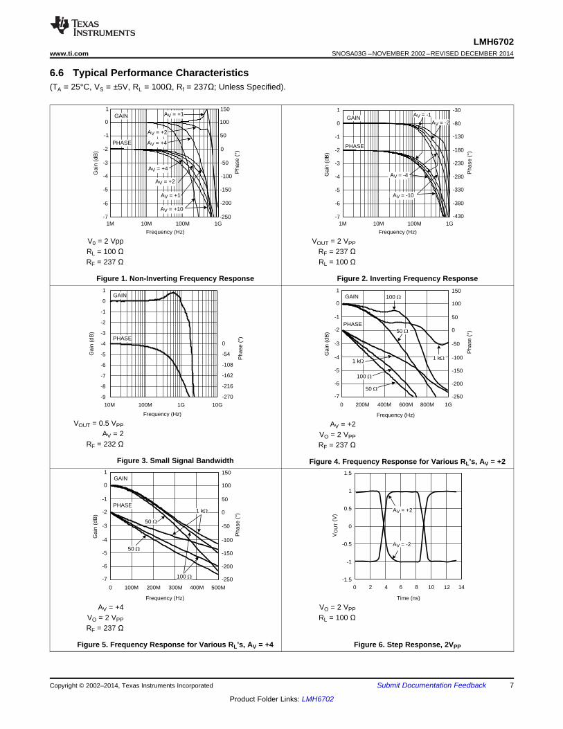
6.6 Typical Performance Characteristics(TA = 25°C, VS = ±5V, RL = 100Ω, Rf = 237Ω; Unless Specified).
V0 = 2 Vpp VOUT = 2 VPPRL = 100 Ω RF = 237 ΩRF = 237 Ω RL = 100 Ω
Figure 1. Non-Inverting Frequency Response Figure 2. Inverting Frequency Response
VOUT = 0.5 VPP AV = +2AV = 2 VO = 2 VPP
RF = 232 Ω RF = 237 Ω
Figure 3. Small Signal Bandwidth Figure 4. Frequency Response for Various RL’s, AV = +2
AV = +4 VO = 2 VPPVO = 2 VPP RL = 100 ΩRF = 237 Ω
Figure 5. Frequency Response for Various RL’s, AV = +4 Figure 6. Step Response, 2VPP
Copyright © 2002–2014, Texas Instruments Incorporated Submit Documentation Feedback 7
Product Folder Links: LMH6702
1 10 100 1k 10k
CL (pF)
0
10
20
30
40
50
60
70
80
90
100
RS
(:)
0
5
10
15
20
25
Set
tling
Tim
e (n
s)
RS
0.05% SETTLING
0.1% SETTLING
-10 -5 0 5 10 15 20
POUT (dBm)
-110
-100
-90
-80
-70
-60
-50
HD
(dB
c)
60MHz
5MHz
10MHz
20MHz
-5 -3 -1 1 3 5-110
-100
-90
-70
-50
-40
PS
(dB
c)
Test Tone Power at 50 : Load (dBm)
25 MHz
50 MHz
75 MHz
-60
-80
1M 10M 100MFrequency (Hz)
-105
-100
-95-90
-85
-80
-75
-70
-65
-60
-40
HD
(dB
c)
-55
-50-45
HD2, RL = 1 k:
HD3, RL = 1 k:
HD2, RL = 100 :
HD3, RL = 100 :
0 10 20 30 40 50 60-4
-3
-2
-1
0
1
3
4V
OU
T (
V)
Time (ns)
2
1 10 100 1kTime (ns)
0.001
0.01
0.1
1
Set
tling
Err
or (
%)
LMH6702SNOSA03G –NOVEMBER 2002–REVISED DECEMBER 2014 www.ti.com
Typical Performance Characteristics (continued)(TA = 25°C, VS = ±5V, RL = 100Ω, Rf = 237Ω; Unless Specified).
RL = 100 ΩAV = +2VOUT = 6 VPP
RL = 100 Ω
Figure 8. Percent Settling vs TimeFigure 7. Step Response, 6VPP
2 VPP AV = +2AV = +2 RL = 100 Ω
RF = 237 Ω RF = 237 Ω
Figure 9. Harmonic Distortion vs. Load and Frequency Figure 10. 2 Tone 3rd Order Spurious Level (SOIC package)(SOIC package)
AV = +2AV = -1RF = 237 ΩRL = 1 kΩRL = 100 Ω
Figure 12. HD2 vs. Output Power (across 100Ω)Figure 11. RS and Settling Time vs. CL(SOIC package)
8 Submit Documentation Feedback Copyright © 2002–2014, Texas Instruments Incorporated
Product Folder Links: LMH6702
1
10
1000
100 1k 10k 100k 1M
FREQUENCY (Hz)
100
10M
INVERTING CURRENT
VOLTAGE
NON-INVERTING
CURRENT
NO
ISE
VO
LTA
GE
(n
V/
Hz)
NO
ISE
CU
RR
EN
T (
pA
/H
z)
0
10
20
30
40
70
CM
RR
/PS
RR
(dB
) 50
60
-55
-45
-35
-25
-15
15
-5
5
20 L
og (
RO
)
1k 10k 100k 1M 10MFrequency (Hz)
100M
+ PSRR
- PSRR
RO
CMRR
-40 -15 10 35 60 85 110 135-10
-8
-4
-2
0
2
-6
8
10
I BI (
µA
)
TEMPERATURE (°C)
UNIT 1
UNIT 3
UNIT 2
4
6
-40 -15 10 35 60 85 110 135-12
-11
-10
-9
-8
-7
-6
-5
-4
I BN
(µ
A)
TEMPERATURE (°C)
UNIT 1
UNIT 3
UNIT 2
-40 -15 10 35 60 85 110 135-4
-3.5
-2.5
-2
-1.5
-1
-3
0.5
VO
S (
mV
)
TEMPERATURE (°C)
UNIT 1
UNIT 3
UNIT 2
-0.5
0
-10 -5 0 5 10 15 20
POUT (dBm)
-120
-110
-90
-80
-70
-60
-50H
D (
dBc)
60 MHz
5 MHz10 MHz
20 MHz
-100
LMH6702www.ti.com SNOSA03G –NOVEMBER 2002–REVISED DECEMBER 2014
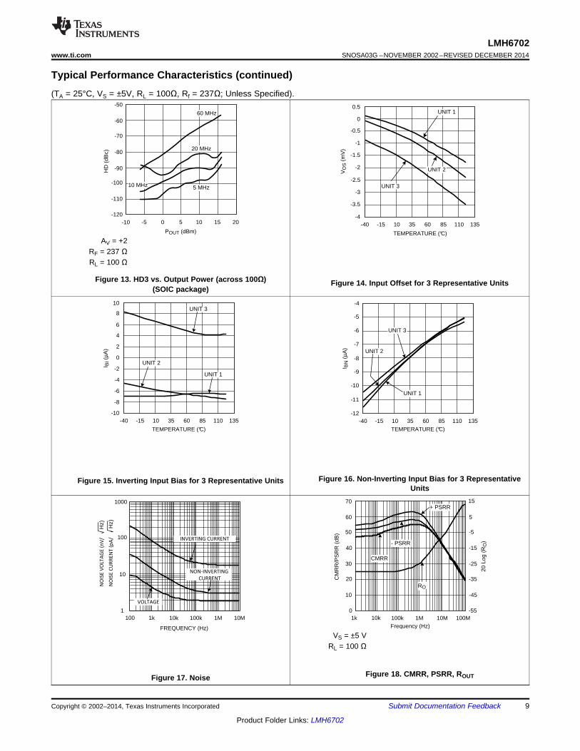
Typical Performance Characteristics (continued)(TA = 25°C, VS = ±5V, RL = 100Ω, Rf = 237Ω; Unless Specified).
AV = +2RF = 237 ΩRL = 100 Ω
Figure 13. HD3 vs. Output Power (across 100Ω) Figure 14. Input Offset for 3 Representative Units(SOIC package)
Figure 16. Non-Inverting Input Bias for 3 RepresentativeFigure 15. Inverting Input Bias for 3 Representative UnitsUnits
VS = ±5 VRL = 100 Ω
Figure 18. CMRR, PSRR, ROUTFigure 17. Noise
Copyright © 2002–2014, Texas Instruments Incorporated Submit Documentation Feedback 9
Product Folder Links: LMH6702

-1.5 1.5
VOUT (V)
-0.03
-0.02
-0.01
0
0.01
0.02
0.03
DP
(°)
DG
DP
0 0.6 1.2-0.009
-0.006
-0.003
0
0.003
0.006
0.009
DG
(%
)
-1.2 -0.6-0.9 -0.3 0.3 0.9
-1.5 1.5
VOUT (V)
-0.03
-0.02
-0.01
0
0.01
0.02
0.03
DG
(%
)
DG
DP
0 0.6 1.2-0.6-1.2
DP
(°)
-0.006
-0.004
-0.002
0
0.002
0.004
0.006
0.3 0.9-0.3-0.910k 1M 10M 100M 1G
Frequency (Hz)
20
30
50
70
90
100
Gai
n (d
B)
100k
MAG
PHASE
40
80
60
110
120
20
40
80
120
160
180
60
140
100
200
220
Pha
se (
°)
LMH6702SNOSA03G –NOVEMBER 2002–REVISED DECEMBER 2014 www.ti.com
Typical Performance Characteristics (continued)(TA = 25°C, VS = ±5V, RL = 100Ω, Rf = 237Ω; Unless Specified).
VS = ±5 V RF = 237 ΩRL = 100 Ω RL = 150 Ω
Figure 19. Transimpedance Figure 20. DG/DP (NTSC)
RF = 237 ΩRL = 150 Ω
Figure 21. DG/DP (PAL)
10 Submit Documentation Feedback Copyright © 2002–2014, Texas Instruments Incorporated
Product Folder Links: LMH6702
1 10 100Frequency (MHz)
-90
-80
-70
-60
-50
-40
-30
HD
2 (d
Bc)
CPOS & CNEG REMOVED
CPOS & CNEG INCLUDED
LMH6702www.ti.com SNOSA03G –NOVEMBER 2002–REVISED DECEMBER 2014
7 Detailed Description
7.1 OverviewThe LMH6702 has been optimized for exceptionally low harmonic distortion while driving very demandingresistive or capacitive loads. Generally, when used as the input amplifier to very high speed flash ADCs, thedistortions introduced by the converter will dominate over the low LMH6702 distortions shown in the TypicalPerformance Characteristics section.
7.2 Feature Description
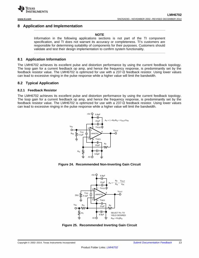
7.2.1 Harmonic DistortionThe capacitor CSS, shown across the supplies in Figure 24 and Figure 25, is critical to achieving the lowest 2nd
harmonic distortion. For absolute minimum distortion levels, it is also advisable to keep the supply decouplingcurrents (ground connections to CPOS, and CNEG in Figure 24 and Figure 25) separate from the groundconnections to sensitive input circuitry (such as RG, RT, and RIN ground connections). Splitting the ground planein this fashion and separately routing the high frequency current spikes on the decoupling caps back to thepower supply (similar to "Star Connection" layout technique) ensures minimum coupling back to the input circuitryand results in best harmonic distortion response (especially 2nd order distortion).
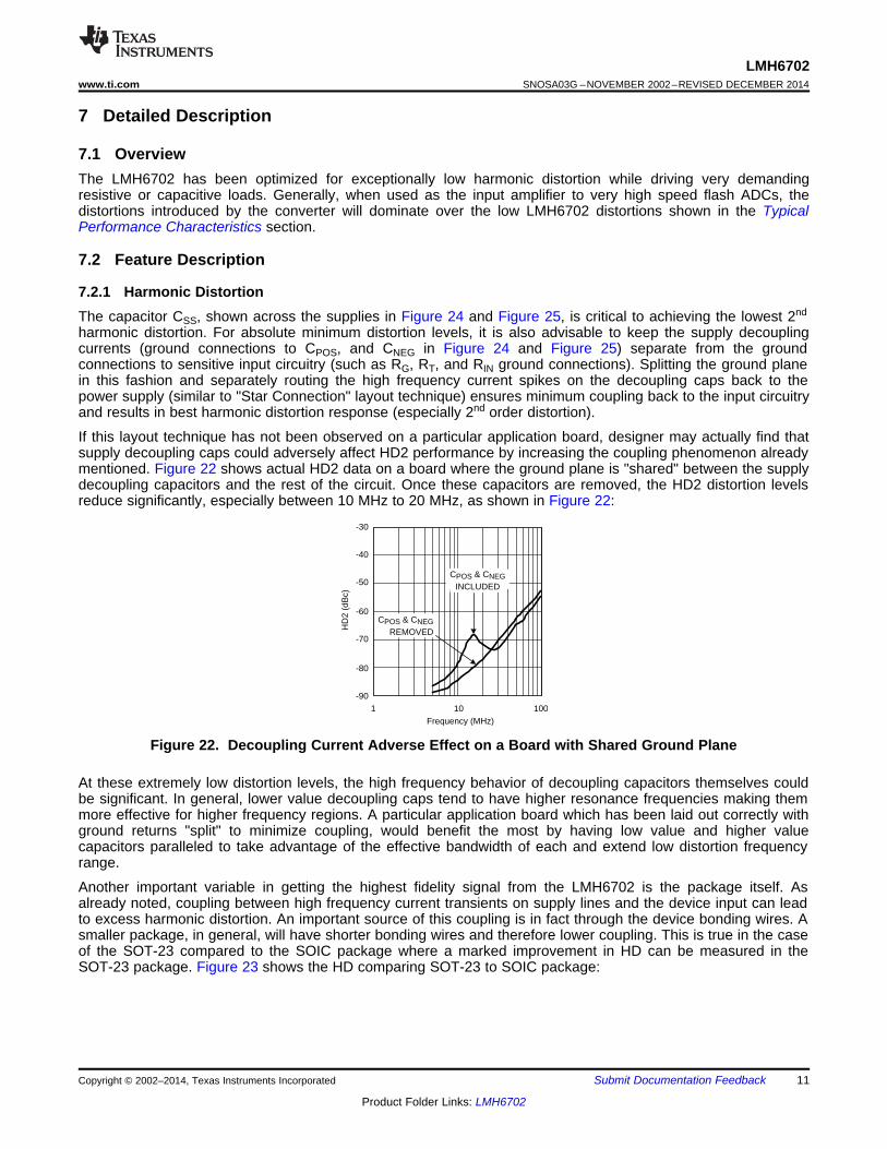
If this layout technique has not been observed on a particular application board, designer may actually find thatsupply decoupling caps could adversely affect HD2 performance by increasing the coupling phenomenon alreadymentioned. Figure 22 shows actual HD2 data on a board where the ground plane is "shared" between the supplydecoupling capacitors and the rest of the circuit. Once these capacitors are removed, the HD2 distortion levelsreduce significantly, especially between 10 MHz to 20 MHz, as shown in Figure 22:
Figure 22. Decoupling Current Adverse Effect on a Board with Shared Ground Plane
At these extremely low distortion levels, the high frequency behavior of decoupling capacitors themselves couldbe significant. In general, lower value decoupling caps tend to have higher resonance frequencies making themmore effective for higher frequency regions. A particular application board which has been laid out correctly withground returns "split" to minimize coupling, would benefit the most by having low value and higher valuecapacitors paralleled to take advantage of the effective bandwidth of each and extend low distortion frequencyrange.
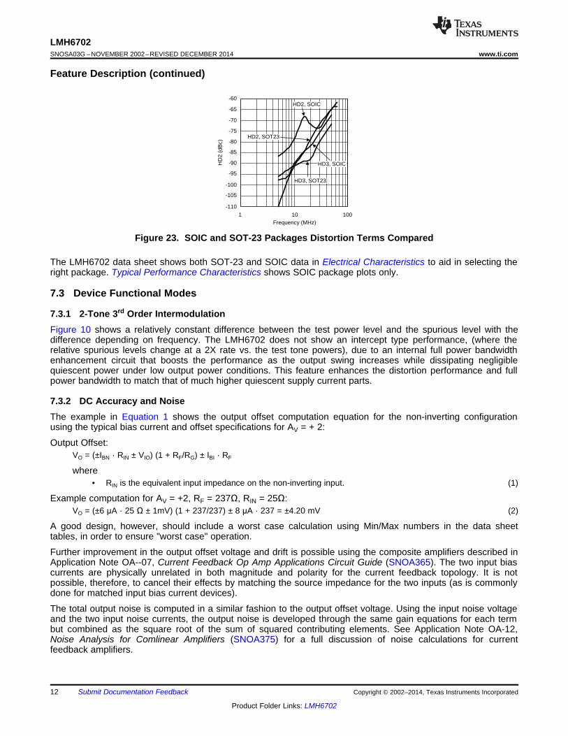
Another important variable in getting the highest fidelity signal from the LMH6702 is the package itself. Asalready noted, coupling between high frequency current transients on supply lines and the device input can leadto excess harmonic distortion. An important source of this coupling is in fact through the device bonding wires. Asmaller package, in general, will have shorter bonding wires and therefore lower coupling. This is true in the caseof the SOT-23 compared to the SOIC package where a marked improvement in HD can be measured in theSOT-23 package. Figure 23 shows the HD comparing SOT-23 to SOIC package:
Copyright © 2002–2014, Texas Instruments Incorporated Submit Documentation Feedback 11
Product Folder Links: LMH6702
1 10 100Frequency (MHz)
-110
-105
-100
-95
-90
-80
-60
HD
2 (d
Bc)
HD3, SOT23
HD2, SOIC
HD2, SOT23
HD3, SOIC
-65
-70
-85
-75
LMH6702SNOSA03G –NOVEMBER 2002–REVISED DECEMBER 2014 www.ti.com
Feature Description (continued)
Figure 23. SOIC and SOT-23 Packages Distortion Terms Compared
The LMH6702 data sheet shows both SOT-23 and SOIC data in Electrical Characteristics to aid in selecting theright package. Typical Performance Characteristics shows SOIC package plots only.
7.3 Device Functional Modes
7.3.1 2-Tone 3rd Order IntermodulationFigure 10 shows a relatively constant difference between the test power level and the spurious level with thedifference depending on frequency. The LMH6702 does not show an intercept type performance, (where therelative spurious levels change at a 2X rate vs. the test tone powers), due to an internal full power bandwidthenhancement circuit that boosts the performance as the output swing increases while dissipating negligiblequiescent power under low output power conditions. This feature enhances the distortion performance and fullpower bandwidth to match that of much higher quiescent supply current parts.
7.3.2 DC Accuracy and NoiseThe example in Equation 1 shows the output offset computation equation for the non-inverting configurationusing the typical bias current and offset specifications for AV = + 2:
Output Offset:VO = (±IBN · RIN ± VIO) (1 + RF/RG) ± IBI · RF
where• RIN is the equivalent input impedance on the non-inverting input. (1)
Example computation for AV = +2, RF = 237Ω, RIN = 25Ω:VO = (±6 μA · 25 Ω ± 1mV) (1 + 237/237) ± 8 μA · 237 = ±4.20 mV (2)
A good design, however, should include a worst case calculation using Min/Max numbers in the data sheettables, in order to ensure "worst case" operation.
Further improvement in the output offset voltage and drift is possible using the composite amplifiers described inApplication Note OA--07, Current Feedback Op Amp Applications Circuit Guide (SNOA365). The two input biascurrents are physically unrelated in both magnitude and polarity for the current feedback topology. It is notpossible, therefore, to cancel their effects by matching the source impedance for the two inputs (as is commonlydone for matched input bias current devices).
The total output noise is computed in a similar fashion to the output offset voltage. Using the input noise voltageand the two input noise currents, the output noise is developed through the same gain equations for each termbut combined as the square root of the sum of squared contributing elements. See Application Note OA-12,Noise Analysis for Comlinear Amplifiers (SNOA375) for a full discussion of noise calculations for currentfeedback amplifiers.
12 Submit Documentation Feedback Copyright © 2002–2014, Texas Instruments Incorporated
Product Folder Links: LMH6702
4
3
2
7
6LMH6702
VOUT+
-
VIN
+5V
-5V
CPOS
6.8µF
RG RF
.01µF
6.8µF
CNEG
.01µF
RT
25: 0.1µF
CSS
SELECT RT TO YIELD DESIRED
RIN = RT||RG
AV = VOUT
VIN
RF
RG=
4
3
2
7
6LMH6702
VOUT+
-
VIN
+5V
-5V
CPOS
6.8µFRG
RF
.01µF
6.8µF
CNEG
.01µF
RIN 0.1µF
CSS
AV = 1 +RF/RG = VOUT/VIN
LMH6702www.ti.com SNOSA03G –NOVEMBER 2002–REVISED DECEMBER 2014
8 Application and Implementation
NOTEInformation in the following applications sections is not part of the TI componentspecification, and TI does not warrant its accuracy or completeness. TI’s customers areresponsible for determining suitability of components for their purposes. Customers shouldvalidate and test their design implementation to confirm system functionality.
8.1 Application InformationThe LMH6702 achieves its excellent pulse and distortion performance by using the current feedback topology.The loop gain for a current feedback op amp, and hence the frequency response, is predominantly set by thefeedback resistor value. The LMH6702 is optimized for use with a 237-Ω feedback resistor. Using lower valuescan lead to excessive ringing in the pulse response while a higher value will limit the bandwidth.
8.2 Typical Application
8.2.1 Feedback ResistorThe LMH6702 achieves its excellent pulse and distortion performance by using the current feedback topology.The loop gain for a current feedback op amp, and hence the frequency response, is predominantly set by thefeedback resistor value. The LMH6702 is optimized for use with a 237-Ω feedback resistor. Using lower valuescan lead to excessive ringing in the pulse response while a higher value will limit the bandwidth.
Figure 24. Recommended Non-Inverting Gain Circuit
Figure 25. Recommended Inverting Gain Circuit
Copyright © 2002–2014, Texas Instruments Incorporated Submit Documentation Feedback 13
Product Folder Links: LMH6702

LMH6702
+
-CIN
ADC
RS
LMH6702SNOSA03G –NOVEMBER 2002–REVISED DECEMBER 2014 www.ti.com
Typical Application (continued)8.2.2 Design RequirementsThe exceptional performance and uniquely targeted superior technical specifications of the LMH6702 make it anatural choice for high speed data acquisition applications as a front end amplifier driving the input of a highperformance ADC. Of these specifications, the following can be discussed in more detail:1. A bandwidth of 1.7 GHz and relative insensitivity of bandwidth to closed loop gain (characteristic of Current
Feedback architecture when compared to the traditional voltage feedback architecture) as shown in Figure 1.2. Ultra-low distortion approaching -87 dBc at the lower frequencies and exceptional noise performance (see
Figure 9 and Figure 17).3. Fast settling in less than 20 ns (see Figure 27).
As the input of an ADC could be capacitive in nature and could also alternate in capacitance value during atypical acquisition cycle, the driver amplifier (LMH6702 in this case) should be designed so that it avoidsinstability, peaking, or other undesirable artifacts.
For Capacitive Load Drive, see Figure 26, which shows a typical application using the LMH6702 to drive anADC.
Figure 26. Input Amplifier to ADC
8.2.3 Detailed Design ProcedureThe series resistor, RS, between the amplifier output and the ADC input is critical to achieving best systemperformance. This load capacitance, if applied directly to the output pin, can quickly lead to unacceptable levelsof ringing in the pulse response. Figure 27 in Application Curve (RS and Settling Time vs. CL) is an excellentstarting point for selecting RS. The value derived in that plot minimizes the step settling time into a fixed discretecapacitive load with the output driving a very light resistive load (1 kΩ). Sensitivity to capacitive loading is greatlyreduced once the output is loaded more heavily. Therefore, for cases where the output is heavily loaded, RSvalue may be reduced. The exact value may best be determined experimentally for these cases.
In applications where the LMH6702 is replacing the CLC409, care must be taken when the device is lightlyloaded and some capacitance is present at the output. Due to the much higher frequency response of theLMH6702 compared to the CLC409, there could be increased susceptibility to low value output capacitance(parasitic or inherent to the board layout or otherwise being part of the output load). As already mentioned, thissusceptibility is most noticeable when the LMH6702's resistive load is light. Parasitic capacitance can beminimized by careful lay out. Addition of an output snubber R-C network will also help by increasing the highfrequency resistive loading.
Referring back to Figure 26, it must be noted that several additional constraints should be considered in drivingthe capacitive input of an ADC. There is an option to increase RS, band-limiting at the ADC input for either noiseor Nyquist band-limiting purposes. However, increasing RS too much can induce an unacceptably large inputglitch due to switching transients coupling through from the "convert" signal. Also, CIN is oftentimes a voltagedependent capacitance. This input impedance non-linearity will induce distortion terms that will increase as RS isincreased. Only slight adjustments up or down from the recommended RS value should therefore be attempted inoptimizing system performance.
14 Submit Documentation Feedback Copyright © 2002–2014, Texas Instruments Incorporated
Product Folder Links: LMH6702

1 10 100 1k 10k
CL (pF)
0
10
20
30
40
50
60
70
80
90
100
RS
(:)
0
5
10
15
20
25
Set
tling
Tim
e (n
s)
RS
0.05% SETTLING
0.1% SETTLING
LMH6702www.ti.com SNOSA03G –NOVEMBER 2002–REVISED DECEMBER 2014
Typical Application (continued)8.2.4 Application Curve
AV = -1RL = 1 kΩ
Figure 27. RS and Settling Time vs. CL
9 Power Supply RecommendationsThe LMH6702 can operate off a single supply or with dual supplies as long as the input CM voltage range(CMIR) has the required headroom to either supply rail. Supplies should be decoupled with low inductance, oftenceramic, capacitors to ground less than 0.5 inches from the device pins. The use of ground plane isrecommended, and as in most high speed devices, it is advisable to remove ground plane close to devicesensitive pins such as the inputs.
10 Layout
10.1 Layout GuidelinesGenerally, a good high frequency layout will keep power supply and ground traces away from the inverting inputand output pins. Parasitic capacitances on these nodes to ground will cause frequency response peaking andpossible circuit oscillations. See Frequent Faux Pas in Applying Wideband Current Feedback Amplifiers,Application Note OA-15 (SNOA367). Texas Instruments suggests the following evaluation boards as a guide forhigh frequency layout and as an aid in device testing and characterization. See Table 1 for details.
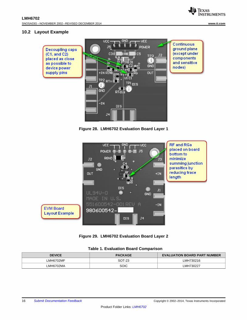
The LMH6702 evaluation board(s) is a good example of high frequency layout techniques as a reference.General high-speed, signal-path layout suggestions include:• Continuous ground planes are preferred for signal routing with matched impedance traces for longer runs.
However, open up both ground and power planes around the capacitive sensitive input and output devicepins as shown in Figure 28. After the signal is sent into a resistor, parasitic capacitance becomes more of abandlimiting issue and less of a stability issue.
• Use good, high-frequency decoupling capacitors (0.1 μF) on the ground plane at the device power pins asshown in Figure 28. Higher value capacitors (2.2 μF) are required, but may be placed further from the devicepower pins and shared among devices. For best high-frequency decoupling, consider X2Y supply-decouplingcapacitors that offer a much higher self-resonance frequency over standard capacitors.
• When using differential signal routing over any appreciable distance, use microstrip layout techniques withmatched impedance traces.
• The input summing junction is very sensitive to parasitic capacitance. Connect any Rf, and Rg elements intothe summing junction with minimal trace length to the device pin side of the resistor, as shown in Figure 29.The other side of these elements can have more trace length if needed to the source or to ground.
Copyright © 2002–2014, Texas Instruments Incorporated Submit Documentation Feedback 15
Product Folder Links: LMH6702
LMH6702SNOSA03G –NOVEMBER 2002–REVISED DECEMBER 2014 www.ti.com
10.2 Layout Example
Figure 28. LMH6702 Evaluation Board Layer 1
Figure 29. LMH6702 Evaluation Board Layer 2
Table 1. Evaluation Board ComparisonDEVICE PACKAGE EVALUATION BOARD PART NUMBER
LMH6702MF SOT-23 LMH730216LMH6702MA SOIC LMH730227
16 Submit Documentation Feedback Copyright © 2002–2014, Texas Instruments Incorporated
Product Folder Links: LMH6702
LMH6702www.ti.com SNOSA03G –NOVEMBER 2002–REVISED DECEMBER 2014
11 Device and Documentation Support
11.1 Documentation Support
11.1.1 Related DocumentationFor related documentation, see the following:• Absolute Maximum Ratings for Soldering (SNOA549)• Current Feedback Op Amp Applications Circuit Guide, Application Note OA--07 (SNOA365)• Frequent Faux Pas in Applying Wideband Current Feedback Amplifiers, Application Note OA-15 (SNOA367)• Noise Analysis for Comlinear Amplifiers, Application Note OA-12 (SNOA375)• Semiconductor and IC Package Thermal Metrics (SPRA953)
11.2 TrademarksVIP10 is a trademark of Texas Instruments.All other trademarks are the property of their respective owners.
11.3 Electrostatic Discharge CautionThese devices have limited built-in ESD protection. The leads should be shorted together or the device placed in conductive foamduring storage or handling to prevent electrostatic damage to the MOS gates.
11.4 GlossarySLYZ022 — TI Glossary.
This glossary lists and explains terms, acronyms, and definitions.
12 Mechanical, Packaging, and Orderable InformationThe following pages include mechanical, packaging, and orderable information. This information is the mostcurrent data available for the designated devices. This data is subject to change without notice and revision ofthis document. For browser-based versions of this data sheet, refer to the left-hand navigation.
Copyright © 2002–2014, Texas Instruments Incorporated Submit Documentation Feedback 17
Product Folder Links: LMH6702
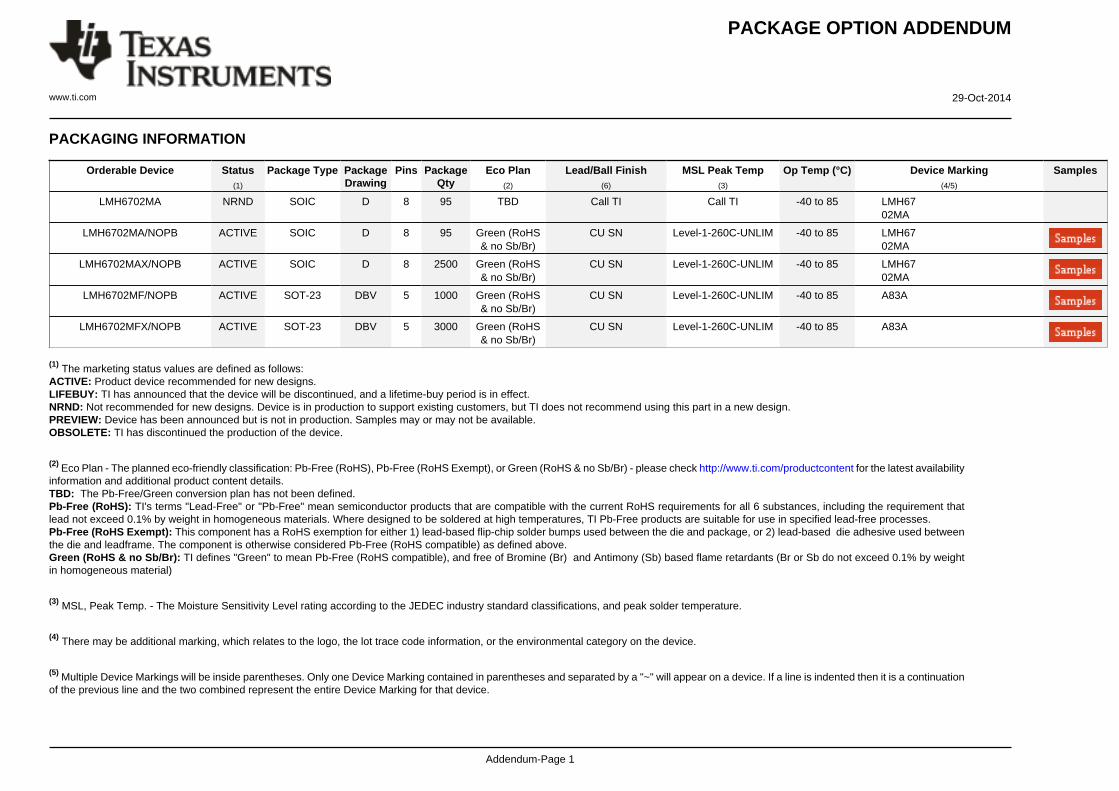
PACKAGE OPTION ADDENDUM
www.ti.com 29-Oct-2014
Addendum-Page 1
PACKAGING INFORMATION
Orderable Device Status(1)
Package Type PackageDrawing
Pins PackageQty
Eco Plan(2)
Lead/Ball Finish(6)
MSL Peak Temp(3)
Op Temp (°C) Device Marking(4/5)
Samples
LMH6702MA NRND SOIC D 8 95 TBD Call TI Call TI -40 to 85 LMH6702MA
LMH6702MA/NOPB ACTIVE SOIC D 8 95 Green (RoHS& no Sb/Br)
CU SN Level-1-260C-UNLIM -40 to 85 LMH6702MA
LMH6702MAX/NOPB ACTIVE SOIC D 8 2500 Green (RoHS& no Sb/Br)
CU SN Level-1-260C-UNLIM -40 to 85 LMH6702MA
LMH6702MF/NOPB ACTIVE SOT-23 DBV 5 1000 Green (RoHS& no Sb/Br)
CU SN Level-1-260C-UNLIM -40 to 85 A83A
LMH6702MFX/NOPB ACTIVE SOT-23 DBV 5 3000 Green (RoHS& no Sb/Br)
CU SN Level-1-260C-UNLIM -40 to 85 A83A
(1) The marketing status values are defined as follows:ACTIVE: Product device recommended for new designs.LIFEBUY: TI has announced that the device will be discontinued, and a lifetime-buy period is in effect.NRND: Not recommended for new designs. Device is in production to support existing customers, but TI does not recommend using this part in a new design.PREVIEW: Device has been announced but is not in production. Samples may or may not be available.OBSOLETE: TI has discontinued the production of the device.
(2) Eco Plan - The planned eco-friendly classification: Pb-Free (RoHS), Pb-Free (RoHS Exempt), or Green (RoHS & no Sb/Br) - please check http://www.ti.com/productcontent for the latest availabilityinformation and additional product content details.TBD: The Pb-Free/Green conversion plan has not been defined.Pb-Free (RoHS): TI's terms "Lead-Free" or "Pb-Free" mean semiconductor products that are compatible with the current RoHS requirements for all 6 substances, including the requirement thatlead not exceed 0.1% by weight in homogeneous materials. Where designed to be soldered at high temperatures, TI Pb-Free products are suitable for use in specified lead-free processes.Pb-Free (RoHS Exempt): This component has a RoHS exemption for either 1) lead-based flip-chip solder bumps used between the die and package, or 2) lead-based die adhesive used betweenthe die and leadframe. The component is otherwise considered Pb-Free (RoHS compatible) as defined above.Green (RoHS & no Sb/Br): TI defines "Green" to mean Pb-Free (RoHS compatible), and free of Bromine (Br) and Antimony (Sb) based flame retardants (Br or Sb do not exceed 0.1% by weightin homogeneous material)
(3) MSL, Peak Temp. - The Moisture Sensitivity Level rating according to the JEDEC industry standard classifications, and peak solder temperature.
(4) There may be additional marking, which relates to the logo, the lot trace code information, or the environmental category on the device.
(5) Multiple Device Markings will be inside parentheses. Only one Device Marking contained in parentheses and separated by a "~" will appear on a device. If a line is indented then it is a continuationof the previous line and the two combined represent the entire Device Marking for that device.
PACKAGE OPTION ADDENDUM
www.ti.com 29-Oct-2014
Addendum-Page 2
(6) Lead/Ball Finish - Orderable Devices may have multiple material finish options. Finish options are separated by a vertical ruled line. Lead/Ball Finish values may wrap to two lines if the finishvalue exceeds the maximum column width.
Important Information and Disclaimer:The information provided on this page represents TI's knowledge and belief as of the date that it is provided. TI bases its knowledge and belief on informationprovided by third parties, and makes no representation or warranty as to the accuracy of such information. Efforts are underway to better integrate information from third parties. TI has taken andcontinues to take reasonable steps to provide representative and accurate information but may not have conducted destructive testing or chemical analysis on incoming materials and chemicals.TI and TI suppliers consider certain information to be proprietary, and thus CAS numbers and other limited information may not be available for release.
In no event shall TI's liability arising out of such information exceed the total purchase price of the TI part(s) at issue in this document sold by TI to Customer on an annual basis.
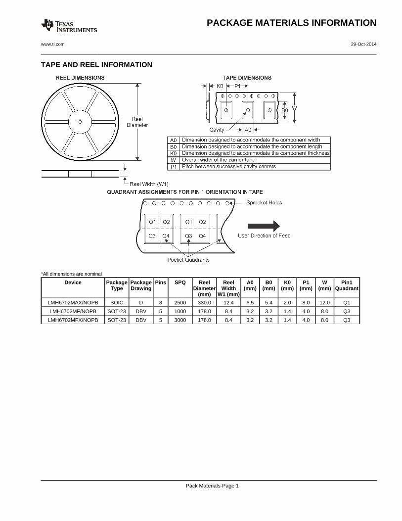
TAPE AND REEL INFORMATION
*All dimensions are nominal
Device PackageType
PackageDrawing
Pins SPQ ReelDiameter
(mm)
ReelWidth
W1 (mm)
A0(mm)
B0(mm)
K0(mm)
P1(mm)
W(mm)
Pin1Quadrant
LMH6702MAX/NOPB SOIC D 8 2500 330.0 12.4 6.5 5.4 2.0 8.0 12.0 Q1
LMH6702MF/NOPB SOT-23 DBV 5 1000 178.0 8.4 3.2 3.2 1.4 4.0 8.0 Q3
LMH6702MFX/NOPB SOT-23 DBV 5 3000 178.0 8.4 3.2 3.2 1.4 4.0 8.0 Q3
PACKAGE MATERIALS INFORMATION
www.ti.com 29-Oct-2014
Pack Materials-Page 1
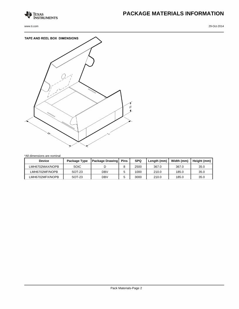
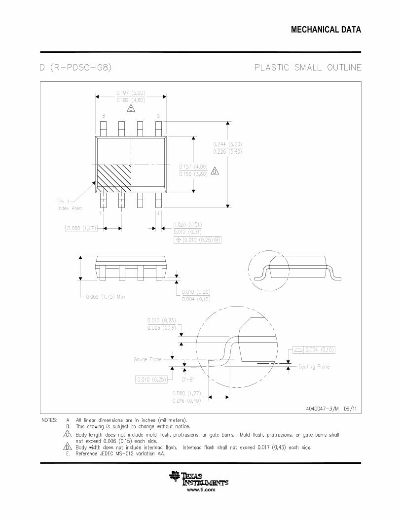
*All dimensions are nominal
Device Package Type Package Drawing Pins SPQ Length (mm) Width (mm) Height (mm)
LMH6702MAX/NOPB SOIC D 8 2500 367.0 367.0 35.0
LMH6702MF/NOPB SOT-23 DBV 5 1000 210.0 185.0 35.0
LMH6702MFX/NOPB SOT-23 DBV 5 3000 210.0 185.0 35.0
PACKAGE MATERIALS INFORMATION
www.ti.com 29-Oct-2014
Pack Materials-Page 2

IMPORTANT NOTICE
Texas Instruments Incorporated and its subsidiaries (TI) reserve the right to make corrections, enhancements, improvements and otherchanges to its semiconductor products and services per JESD46, latest issue, and to discontinue any product or service per JESD48, latestissue. Buyers should obtain the latest relevant information before placing orders and should verify that such information is current andcomplete. All semiconductor products (also referred to herein as “components”) are sold subject to TI’s terms and conditions of salesupplied at the time of order acknowledgment.TI warrants performance of its components to the specifications applicable at the time of sale, in accordance with the warranty in TI’s termsand conditions of sale of semiconductor products. Testing and other quality control techniques are used to the extent TI deems necessaryto support this warranty. Except where mandated by applicable law, testing of all parameters of each component is not necessarilyperformed.TI assumes no liability for applications assistance or the design of Buyers’ products. Buyers are responsible for their products andapplications using TI components. To minimize the risks associated with Buyers’ products and applications, Buyers should provideadequate design and operating safeguards.TI does not warrant or represent that any license, either express or implied, is granted under any patent right, copyright, mask work right, orother intellectual property right relating to any combination, machine, or process in which TI components or services are used. Informationpublished by TI regarding third-party products or services does not constitute a license to use such products or services or a warranty orendorsement thereof. Use of such information may require a license from a third party under the patents or other intellectual property of thethird party, or a license from TI under the patents or other intellectual property of TI.Reproduction of significant portions of TI information in TI data books or data sheets is permissible only if reproduction is without alterationand is accompanied by all associated warranties, conditions, limitations, and notices. TI is not responsible or liable for such altereddocumentation. Information of third parties may be subject to additional restrictions.Resale of TI components or services with statements different from or beyond the parameters stated by TI for that component or servicevoids all express and any implied warranties for the associated TI component or service and is an unfair and deceptive business practice.TI is not responsible or liable for any such statements.Buyer acknowledges and agrees that it is solely responsible for compliance with all legal, regulatory and safety-related requirementsconcerning its products, and any use of TI components in its applications, notwithstanding any applications-related information or supportthat may be provided by TI. Buyer represents and agrees that it has all the necessary expertise to create and implement safeguards whichanticipate dangerous consequences of failures, monitor failures and their consequences, lessen the likelihood of failures that might causeharm and take appropriate remedial actions. Buyer will fully indemnify TI and its representatives against any damages arising out of the useof any TI components in safety-critical applications.In some cases, TI components may be promoted specifically to facilitate safety-related applications. With such components, TI’s goal is tohelp enable customers to design and create their own end-product solutions that meet applicable functional safety standards andrequirements. Nonetheless, such components are subject to these terms.No TI components are authorized for use in FDA Class III (or similar life-critical medical equipment) unless authorized officers of the partieshave executed a special agreement specifically governing such use.Only those TI components which TI has specifically designated as military grade or “enhanced plastic” are designed and intended for use inmilitary/aerospace applications or environments. Buyer acknowledges and agrees that any military or aerospace use of TI componentswhich have not been so designated is solely at the Buyer's risk, and that Buyer is solely responsible for compliance with all legal andregulatory requirements in connection with such use.TI has specifically designated certain components as meeting ISO/TS16949 requirements, mainly for automotive use. In any case of use ofnon-designated products, TI will not be responsible for any failure to meet ISO/TS16949.
Products ApplicationsAudio www.ti.com/audio Automotive and Transportation www.ti.com/automotiveAmplifiers amplifier.ti.com Communications and Telecom www.ti.com/communicationsData Converters dataconverter.ti.com Computers and Peripherals www.ti.com/computersDLP® Products www.dlp.com Consumer Electronics www.ti.com/consumer-appsDSP dsp.ti.com Energy and Lighting www.ti.com/energyClocks and Timers www.ti.com/clocks Industrial www.ti.com/industrialInterface interface.ti.com Medical www.ti.com/medicalLogic logic.ti.com Security www.ti.com/securityPower Mgmt power.ti.com Space, Avionics and Defense www.ti.com/space-avionics-defenseMicrocontrollers microcontroller.ti.com Video and Imaging www.ti.com/videoRFID www.ti-rfid.comOMAP Applications Processors www.ti.com/omap TI E2E Community e2e.ti.comWireless Connectivity www.ti.com/wirelessconnectivity
Mailing Address: Texas Instruments, Post Office Box 655303, Dallas, Texas 75265Copyright © 2015, Texas Instruments Incorporated