slus537c − august 2002 − revised march 2004 ˘ ˇ ˆ ˆ · slus537c − august 2002 − revised...
TRANSCRIPT
SLUS537C − AUGUST 2002 − REVISED MARCH 2004
FEATURES
Integrated Power Interface Switch for IEEE802.3af Powered Devices (PDs)
Provides PD Detection Signature
Provides PD Classification Signature(Class 0−4)
Programmable Inrush Current Limit
Internal 0.3- Ω Low-Side FET
Interfaces to DC/DC Soft-Start for DC/DCEnable
Internal Thermal Protection – Disconnects PDLoad
Minimal External Parts Count
8-Pin SOIC, 8-Pin TSSOP Packages
APPLICATIONS
VoIP Phones
Internet Appliances
Wireless LAN Access Points
Bluetooth Access Points
DESCRIPTION
Acting as an interface between the power sourcingequipment (PSE) and the powered device (PD), theTPS2370 performs all detection, classification, inrushcurrent limiting, and switch FET control that isnecessary for compliance with the IEEE 802.3afStandard. An internal 0.3-Ω FET provides maximumpower delivery. As an additional feature, the TPS2370interfaces with the enable/soft-start signal of a dc-to-dcconverter, eliminating the need to have an accurateUVLO in the dc-to-dc converter.
At low input voltages (1.8 V to 10 V), the TPS2370draws less than 12 µA, allowing accurate sensing of theexternal 24.9-kΩ discovery resistor. At input voltagesbetween 15 V and 20 V, an external resistor sets thelevel of current to be drawn during classification mode.TPS2370 is compatible with current as well as voltagemeasurement schemes for classification. Above 20-Vinput, the classification current is shut off, reducinginternal power dissipation.
The TPS2370 drives an internal low-side FET forcontrol of the return side of the power path. The internalFET is turned on when the input voltage reaches 40 Vand above. When the input voltage decreases, the FETremains on until the input voltage drops to below 30 V.
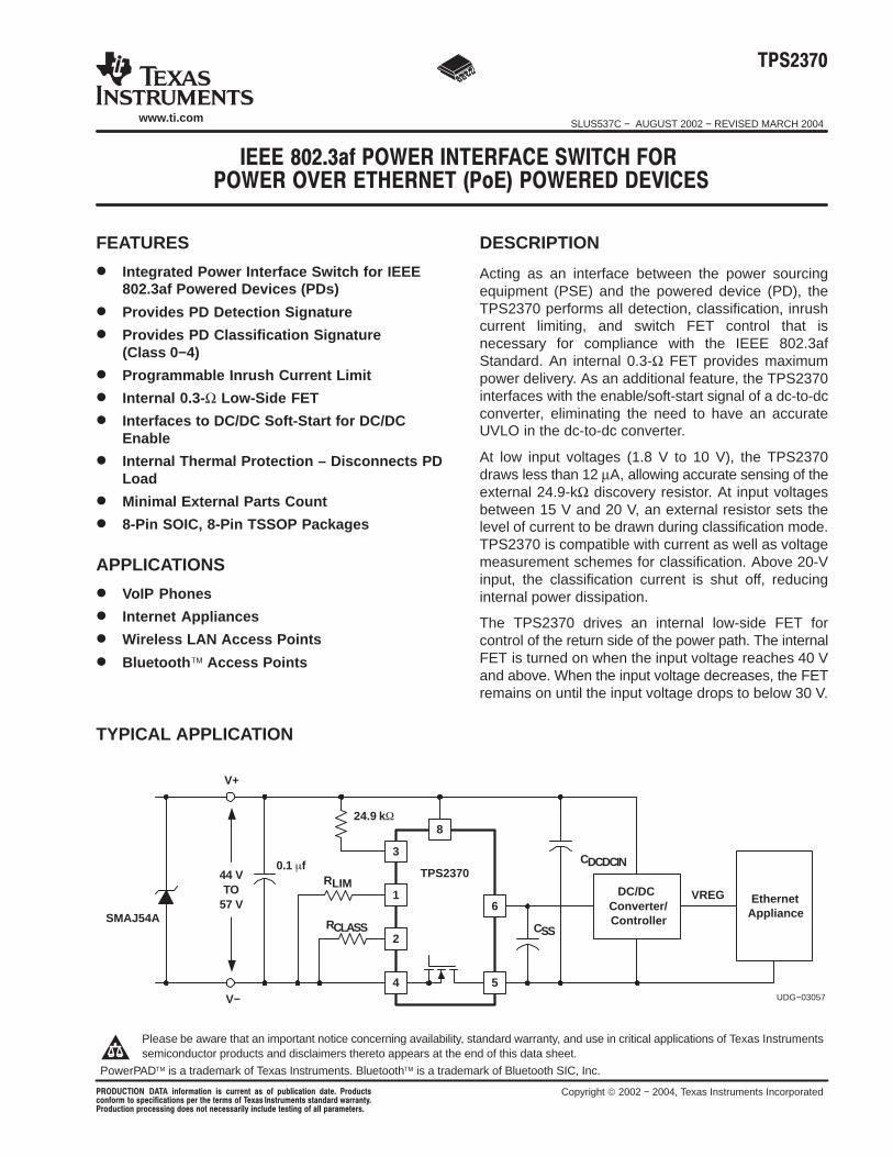
TYPICAL APPLICATION
3
1
2
4 5
TPS2370
6DC/DC
Converter/Controller
8
EthernetAppliance
VREG
44 VTO
57 V
V+
V−
SMAJ54A
24.9 k
RLIM
CSS
CDCDCIN
RCLASS
UDG−03057
0.1 f
! " #$%! " &$'(#! )!% )$#!"# ! "&%# #!" &% !*% !%" %+" "!$%!" "!)) ,!-)$#! &#%"". )%" ! %#%""(- #($)% !%"!. (( &%!%"
PowerPAD is a trademark of Texas Instruments. Bluetooth is a trademark of Bluetooth SIC, Inc.
Please be aware that an important notice concerning availability, standard warranty, and use in critical applications of Texas Instrumentssemiconductor products and disclaimers thereto appears at the end of this data sheet.
www.ti.com
Copyright 2002 − 2004, Texas Instruments Incorporated
SLUS537C − AUGUST 2002 − REVISED MARCH 2004
www.ti.com
2
DESCRIPTION (CONTINUED)During initial turnon of the switch (inrush mode), an external resistor is used to program the inrush current, allowing a widerange of capacitor values to be used at the load. According to IEEE 802.3af specification, inrush current of 400 mA isallowed only for 50 ms, limiting the load capacitor to approximately 180 µF. A programmable inrush current limit removesthis limitation, allowing a larger capacitor to be used with a lower inrush current limit.
These devices have limited built-in ESD protection. The leads should be shorted together or the device placed in conductive foam duringstorage or handling to prevent electrostatic damage to the MOS gates.
ORDERING INFORMATION
TA PACKAGE (1) PART NUMBER
0°C to 70°CPlastic TSSOP (PW) TPS2370PW
0°C to 70°CPlastic SOIC (D) TPS2370D
(1) The PW and D packages are also available taped and reeled. Add an R suffix to the device type (i.e., TPS2370PWR).
ABSOLUTE MAXIMUM RATINGSOver operating free-air temperature range unless otherwise noted (2)
TPS2370 UNIT
ILIM 4
Input voltage range, wrt VEECLASS 12
VInput voltage range, wrt VEE DET, RTN, EN_DC, VDD 68V
EN_DC (wrt RTN) 5
Operating junction temperature range, TJ −55 to 150 °C
Storage temperature, Tstg −65 to 150 °C
Lead temperature 1,6 mm (1/16 inch) from case for 10 seconds 300 °C(2) Stresses beyond those listed under “absolute maximum ratings” may cause permanent damage to the device. These are stress ratings only,and functional operation of the device at these or any other conditions beyond those indicated under “recommended operating conditions” is notimplied. Exposure to absolute-maximum-rated conditions for extended periods may affect device reliability.
RECOMMENDED OPERATING CONDITIONSMIN NOM MAX UNIT
Input voltage, VI 48 57 V
Operating junction temperature, TJ 0 70 °C
DISSIPATION RATINGS (3)(4)
PACKAGETHERMAL IMPEDANCEJUNCTION-TO-AMBIENT
TA < 25°CPOWER RATING
TA = 25°CDERATINGFACTOR
TA = 70°CPOWER RATING
8-Pin Plastic TSSOP (PW) 258.5°C/W 464 mW 3.9 mW/°C 290 mW
8-Pin Plastic SOIC (D) 176.0°C/W 682 mW 5.7 mW/°C 426 mW(3) Test board conditions:
1. 3” x 3”, 4 layers, thickness: 0.062”2. 1.5 oz. copper traces located on the top of the PCB3. 1.5 oz. copper ground plane on the bottom of the PCB4. 0.5 oz. copper ground planes on the 2 internal layers5. 12 thermal vias
(4) Maximum power dissipation may be limited by overcurrent protection.
SLUS537C − AUGUST 2002 − REVISED MARCH 2004
www.ti.com
3
ELECTRICAL CHARACTERISTICS VDD = 48 V; TA = 0°C to 70°C; all voltages and currents are with respect to VEE; (unless otherwise noted)
PARAMETER TEST CONDITIONS MIN TYP MAX UNIT
SUPPLY
Offset current VDD = 1.8 V, DET = OPEN 3
IDD Sleep current 1.8 V ≤ VDD < 10 V, DET = OPEN 5 12A
IDET Detection load currentRDET = 24.9 kΩ, VDD = 1.8 V 70 73 76
µA
IDET Detection load currentRDET = 24.9 kΩ, VDD = 9.5 V 380 390 400
Classification current thresholdTurn on 10.0 12.5 14.0
VClassification current thresholdTurn off 21.5 22.5 23.5
V
VDD current class 00.44 W ≤ PPoE ≤ 12.95 W,15 V ≤ VDD ≤ 20 V, RCLASS = 4.42 kΩ 2.2 2.5 2.8
VDD current class 10.44 W ≤ PPoE ≤ 3.84 W,15 V ≤ VDD ≤ 20 V, RCLASS = 953 Ω 10.4 10.8 11.5
VDD current class 23.84 W ≤ PPoE ≤ 6.49 W,15 V ≤ VDD ≤ 20 V, RCLASS = 549 Ω 18.1 18.6 19.5 mA
VDD current class 36.49 W ≤ PPoE ≤ 12.95 W,15 V ≤ VDD ≤ 20 V, RCLASS = 357 Ω 27.7 28.4 29.9
VDD current class 4Reserved for future use,15 V ≤ VDD ≤ 20 V, RCLASS = 255 Ω 38.5 39.6 42.0
VDD quiescent current 30 V ≤ VDD ≤ 57 V, RCLASS = 255 Ω 500 800 µA
Input UVLO thresholdTurn on 38.6 40.2 41.8
Input UVLO thresholdTurn off 30.2 31.4 32.6 V
UVLO hysteresis 7.8 8.8 9.8
V
EN_DC sink current 40 80 200 µA
RTN threshold for EN_DC 1.2 1.5 1.8 V
DMOS RDS(on) IRTN = 200 mA 0.15 0.30 0.60 Ω
Full load current limit VRTN < 1.5 V 405 455 505mA
ILIM current limit programming RLIM = 125 kΩ, VRTN > 1.5 V during startup 180 250 300mA
Thermal shutdown temperature 144°C
Thermal shutdown hysteresis 20°C
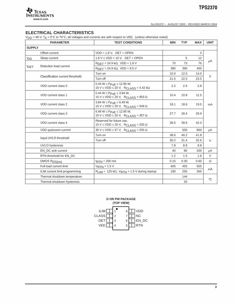
1
2
3
4
8
7
6
5
ILIMCLASS
DETVEE
VDDNCEN_DCRTN
D OR PW PACKAGE(TOP VIEW)
SLUS537C − AUGUST 2002 − REVISED MARCH 2004
www.ti.com
4
TERMINAL FUNCTIONSTERMINAL
I/O DESCRIPTIONNAME NO.
I/O DESCRIPTION
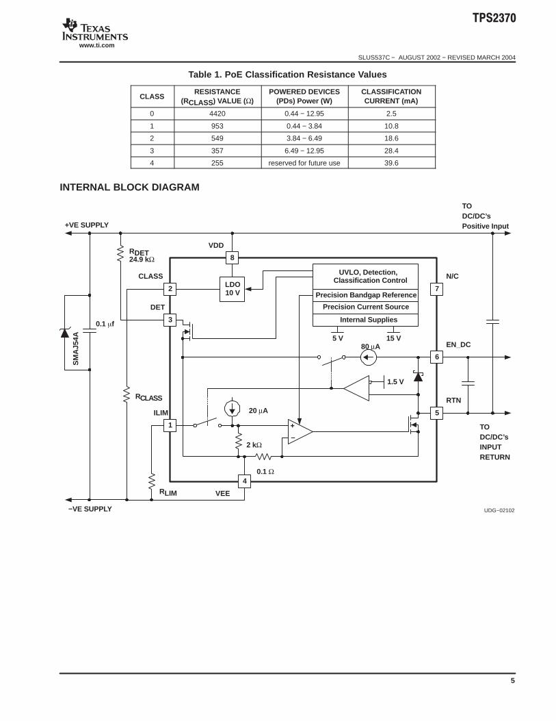
CLASS 2 OSets classification level with a single resistor to VEE. A precision voltage of 10 V is applied to this pin duringclassification. RCLASS values listed in Table 1.
DET 3 O Connect the 24.9-kΩ detection resistor (RDET) between this pin and VDD.
EN_DC 6 O Ties to dc-to-dc converter’s shutdown or soft-start pin. Sinks 80 µA until the load capacitor is fully charged.
ILIM 1 OSets start-up current limit level with a resistor to VEE. If using CDC2DCIN > 180 µF, IRUSH must be less than400 mA. Extra capacitance on ILIM pin can cause oscillations in the current waveform.
RTN 5 O Return pin. Connect this pin to input return side of the dc-to-dc converter.
VDD 8 I Connection to PD input port positive voltage.
VEE 4 I Input side power return for the controller.
(1) IINRUSH 450 mA 25 kRLIM (1 A)
DETAILED PIN DESCRIPTIONS
ILIM (Pin 1)
Inrush current limiting pin. This pin is used to program the inrush current of the device. By placing a resistor to VEEfrom this pin, the inrush current into the load is limited via the following equation:
IINRUSH 450 mA 25 kRLIM (1 A)
CLASS (Pin 2)
Classification pin. The PD can be optionally classified by adding a resistor from this pin to ground. The resistor specificto each class is given in Table 1: PoE Classification Resistance Values.
DET (Pin3)
Detection pin. This pin is used to set up the detection resistance during PD detection. By tying a resistor, RDET, fromthis pin to VDD, the user sets the detection resistance. It should be noted that the device itself looks like approximately1 MΩ of resistance in parallel with RDET.
VEE (Pin 4)
Negative supply to the device.
RET (Pin 5)
Negative supply to the load. This pin is the drain side of a FET between the RET pin and the VEE pin, providing hotswap capabilities to the load. When the FET is switched on, there is approximately 300 mΩ between this pin and VEE.
EN_DC (Pin 6)
Enable pin for the load. This pin is intended to be used with a dc-to-dc coverter with a soft start capacitor. When poweris not available to the dc-to-dc converter, this pin sinks 80 µA and holds off the soft-start capacitor on the dc-to-dcconverter. Once the voltage across the load is within 1.5 V of its final value, the EN_DC pin stops drawing currentand becomes high impedance, allowing the dc-to-dc converter to soft start normally.
VDD (Pin 8)
Positive supply to the device.
(1)
SLUS537C − AUGUST 2002 − REVISED MARCH 2004
www.ti.com
5
Table 1. PoE Classification Resistance Values
CLASSRESISTANCE
(RCLASS) VALUE (Ω)POWERED DEVICES
(PDs) Power (W)CLASSIFICATIONCURRENT (mA)
0 4420 0.44 − 12.95 2.5
1 953 0.44 − 3.84 10.8
2 549 3.84 − 6.49 18.6
3 357 6.49 − 12.95 28.4
4 255 reserved for future use 39.6
INTERNAL BLOCK DIAGRAM
2
CLASS
3
DET
1
ILIM
4
VEE
5
RTN
6
EN_DC
7
N/C
8
VDD
LDO10 V
UVLO, Detection,Classification Control
Precision Bandgap Reference
Precision Current Source
Internal Supplies
5 V 15 V
1.5 V
+
80 µA
20 µA
2 kΩ
0.1 Ω
RDET24.9 kΩ
RCLASS
RLIM
−VE SUPPLY
+VE SUPPLY
TODC/DC’sPositive Input
TODC/DC’sINPUTRETURN
UDG−02102
0.1 f
SM
AJ5
4A
SLUS537C − AUGUST 2002 − REVISED MARCH 2004
www.ti.com
6
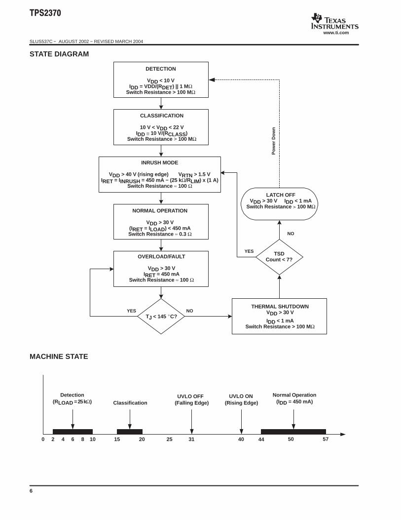
STATE DIAGRAM
YES NO
YES
NO
Pow
er D
own
DETECTION
VDD < 10 VIDD = VDD/(RDET) || 1 MΩ
Switch Resistance > 100 M Ω
CLASSIFICATION
10 V < VDD < 22 VIDD ≅ 10 V/(RCLASS)
Switch Resistance > 100 MΩ
INRUSH MODE
VDD > 40 V (rising edge) V RTN > 1.5 VIRET = IINRUSH = 450 mA − (25 k Ω/RLIM) x (1 A)
Switch Resistance ≈ 100 Ω
NORMAL OPERATION
VDD > 30 V(IRET = ILOAD) < 450 mASwitch Resistance ≈ 0.3 Ω
OVERLOAD/FAULT
VDD > 30 VIRET = 450 mA
Switch Resistance ≈ 100 Ω
TJ < 145 C?
THERMAL SHUTDOWNVDD > 30 V
IDD < 1 mASwitch Resistance > 100 M Ω
TSDCount < 7?
LATCH OFFVDD > 30 V IDD < 1 mA
Switch Resistance 100 MΩ
MACHINE STATE
0 50
Classification (Falling Edge)
44 57
UVLO ON(Rising Edge)
2 4 6 8 10 15 20 3125 40
UVLO OFFDetection(RLOAD = 25 kΩ)
Normal Operation(IDD = 450 mA)
SLUS537C − AUGUST 2002 − REVISED MARCH 2004
www.ti.com
7
APPLICATION INFORMATION
OVERVIEW
With the addition of power via media-dependent interface (MDI) to the IEEE 802.3af Standard, all data terminalequipment (DTE) now has the option to receive power over existing cabling that is used for data transmission.The IEEE 802.3af Standard defines the requirements associated with providing and receiving power over theexisting cabling. The power sourcing equipment (PSE) provides the power on the cable and the powered device(PD) receives the power. As part of the IEEE 802.3af Standard, the interface between the PSE and PD isdefined as it relates to the detection and classification protocol.
POWER SOURCING EQUIPMENT DETECTION OF A POWERED DEVICE
A powered device (PD) draws power or requests power by participating in a PD detection algorithm. Thisalgorithm requires the power sourcing equipment (PSE) to probe the link looking for a valid PD. The PSE probesthe link by sending out a voltage between 2.8 V and 10 V across the power lines. A valid PD detects this voltageand places a resistance of between 23.75 kΩ and 26.25 kΩ across the power lines. Naturally, the current variesdepending on the input voltage. On detecting this current, the PSE concludes that a valid PD is connected at theend of the ethernet cable and is requesting power.
If the powered device (PD) is in a state in which it does not accept power, the PD is required to place aresistance above or below the values listed for a valid PD. On the lower end, a range between 12 kΩ and23.75 kΩ signifies that the PD does not require power. On the higher end, the range is defined to be between26.25 kΩ and 45 kΩ . Any resistance value less than 12 kΩ and greater than 45 kΩ, is interpreted by the PSEas a nonvalid PD detection signature.
The TPS2370 participates in the detection algorithm by activating an internal FET, which connects the DET pin ofthe device to VEE. As a result, any resistance connected between VDD and the DET pin of the TPS2370 is, ineffect, across the power lines. This internal FET is active only when input power to the PD is between 2.8 V and10 V.
POWER SOURCING EQUIPMENT CLASSIFICATION OF A POWERED DEVICE
After the detection phase, the PSE can optionally initiate a classification of the PD. The classification of a PD isused by the PSE to determine the maximum power required by the PD during normal operation. Five differentlevels of classification are defined by the IEEE 802.3af Standard. These levels are shown in Table 2.
Table 2. Powered Device Classification Levels
CLASS USAGE
POWER DEVICEPOWER
(W)
CLASSIFICATIONCURRENT
(mA)
MIN MAX MIN MAX
0 Default 0.44 12.95 0 4
1 Optional 0.44 3.84 9 12
2 Optional 3.84 6.49 17 20
3 Optional 6.49 12.95 26 30
4 Not allowed reserved for future use 36 44
Classification of the PD is optionally performed by the PSE only after a valid PD has been detected. Todetermine PD classification, the PSE increases the voltage across the power lines to between 15.5 V and 20.5 V.The amount of current drawn by the PD determines the classification (see Table 2).
When the input voltage to the TPS2370 is between 14.0 V and 20.5 V, the TPS2370 uses an internal regulator togenerate a fixed voltage on the CLASS pin. A resistor connected between the CLASS pin and VEE draws a fixedamount of current and thereby defines the classification level of the PD.
SLUS537C − AUGUST 2002 − REVISED MARCH 2004
www.ti.com
8
APPLICATION INFORMATION
POWER SOURCING EQUIPMENT POWER TO THE POWERED DEVICE
On completion of the detection and optional classification phases, the PSE ramps its output voltage above 42 V .Once the UVLO threshold has been reached, the internal FET is turned on. At this point, the PD begins tooperate normally and it continues to operate normally as long as the input voltage remains above 30 V. For mostPDs, this input voltage is down-converted using an onboard dc-to-dc converter to generate the required voltages.
The TPS2370 is designed to apply the PSE output voltage of 36 V to 57 V across the input of the onboarddc-to-dc converter. This is accomplished on the TPS2370 by turning on an internal pass FET located across thepower return.
PROGRAMMING THE INRUSH CURRENT
During the initial turnon of the pass FET, an inrush current is created from the charging of the capacitance at theinput of the dc-to-dc converter. According to the IEEE 802.3af specification, if the input capacitance is less than180 µF, the PSE limits the inrush current. If the input capacitance is greater than 180 µF, the IEEE 802.3afspecification requires the PD to limit the inrush current to less than 400 mA.
In order to satisfy the IEEE 802.3af requirements, the TPS2370 has been designed for a typical current limit of450 mA. This current limit setting satisfies the normal operation requirements as well as the inrush requirementsfor a capacitive load of 180 µF or less. If a larger load capacitor is desired, the TPS2370 has been designed witha programmable inrush current limit feature. This feature allows the designer the option of using a capacitorlarger than 180 µF. Note that the inrush current feature may also be used to lower voltage drops in the cablingbetween the PSE and the PD during start-up.
The programmable inrush current limit has a range of 50 mA to 449 mA. The limit is set by connecting anexternal resistor from ILIM (pin 1) to VEE (pin 4) of the TPS2370. Equation (1) shows the calculation for theprogrammable inrush current limit.
IINRUSH 450 mA 25 kRLIM (1 A)
where RLIM is a value between 63.5 kΩ and 25 MΩ.
USING EN_DC AS A SOFT-START OR A POWER-GOOD FUNCTION
The EN_DC pin is an output intended for use as a soft-start for a dc-to-dc converter. During the initial turnon ofthe pass FET, an internal 80-µA current sink is enabled on the EN_DC pin. This internal current sink is removedonly after the load capacitance has been charged to within 1.5-V of the supply voltage. By connecting theEN_DC output to the soft-start capacitor of a dc-to-dc converter, the internal current sink keeps the dc-to-dcconverter off during start-up. Once the voltage across the converter has reached within 1.5 V of full voltage, thedc-to-dc converter is allowed to soft start.
For operation as a power-good output, the EN_DC requires an external pull-up resistor. A 1-MΩ resistor isrecommended. The EN_DC output also requires a clamp to limit the output voltage to within recommendedoperating levels. A 5-V zener diode connected between EN_DC and RTN (pin 5 of the TPS2370) isrecommended. This configuration allows the EN_DC pin to act as an open-drain output with which manydesigners are more familiar.
(2)
SLUS537C − AUGUST 2002 − REVISED MARCH 2004
www.ti.com
9
APPLICATION INFORMATION
SURGE SUPPRESSION
As specified in the Absolute Maximum Ratings table, the absolute maximum input voltage of the TPS2370 is68 V. The IEEE 802.3af Power-over-Ethernet Standard specifies the voltage range of PSE output as between44 V and 57 V. This PSE output voltage range would be reduced by cable, connector, and other IR dropsbetween the PSE and the TPS2370 in the PD. However, the use of extended cable lengths and transformers insome applications may induce transients in excess of 68 V during a hot plug event. To manage these transientevents and keep them from significantly exceeding the application’s maximum voltage, a transorb such as theSMAJ54A should be placed between the positive input supply, VDD (pin 8), and the negative input supply, VEE(pin 4). This, combined with a 0.1-µF bypass capacitor in parallel with the transorb, helps to protect the TPS2370from damage caused by transients during hot plug events. The transorb or zener diode should be selected suchthat it does not zener below the maximum required application voltage of 57 V, but before reaching the 68-Vabsolute maximum rating. For layout purposes, the 0.1-µF capacitor should be placed as close as possible to thedevice; the transorb or zener diode should be placed as close to the supply connector as possible. Based on thenature of the PD application, these measures should be considered an implementation requirement.
USE OF BARREL RECTIFIERS
Many applications use barrel rectifiers after the RJ-45 connector in order to be polarity insensitive. Barrelrectifiers in front of the TPS2370 cause the voltages at the device to be lower than the voltages at the RJ-45.The TPS2370 allows for this and is IEEE802.3af compliant during the detection and classification phases. Forthe detection phase, the device begins detection for voltages as low as 1.3 V across the supply pins. For theoptional classification phase, the device is guaranteed to start classification below 14 V across the supply pins.Once classification has been engaged, it becomes latched-in and further voltage drops due to cable resistanceand class current does not cause it to switch out of classification. Thus, the TPS2370 allows for at least a 1.5-Vdrop between the RJ-45 and the TPS2370 due to barrel rectifiers during both detection and classification phases.
However, in cases where the PSE is operating at the minimum class voltage (15.5 V) and there is a 20-Ω, 100-mcable between the PSE and the PD, class 3 devices may not classify correctly when using barrel rectifiers. Class3 device designs should include Schottky diodes to handle all corner cases, or switch to class 0 devices whenusing barrel rectifiers.
THERMAL SHUTDOWN
In the event of a short circuit or overload condition, the TPS2370 begins to heat up until thermal shutdown isreached. Once thermal shutdown is reached, the internal FET is switched off, removing the load from the supply.After the device has cooled sufficiently, it retries by restarting the internal FET. If the overload or short is notremoved, the device cycles thermal shutdown seven times before latching the internal FET off. Once the internalFET is latched off, power needs to be cycled to reset the latch.
SLUS537C − AUGUST 2002 − REVISED MARCH 2004
www.ti.com
10
APPLICATION INFORMATION
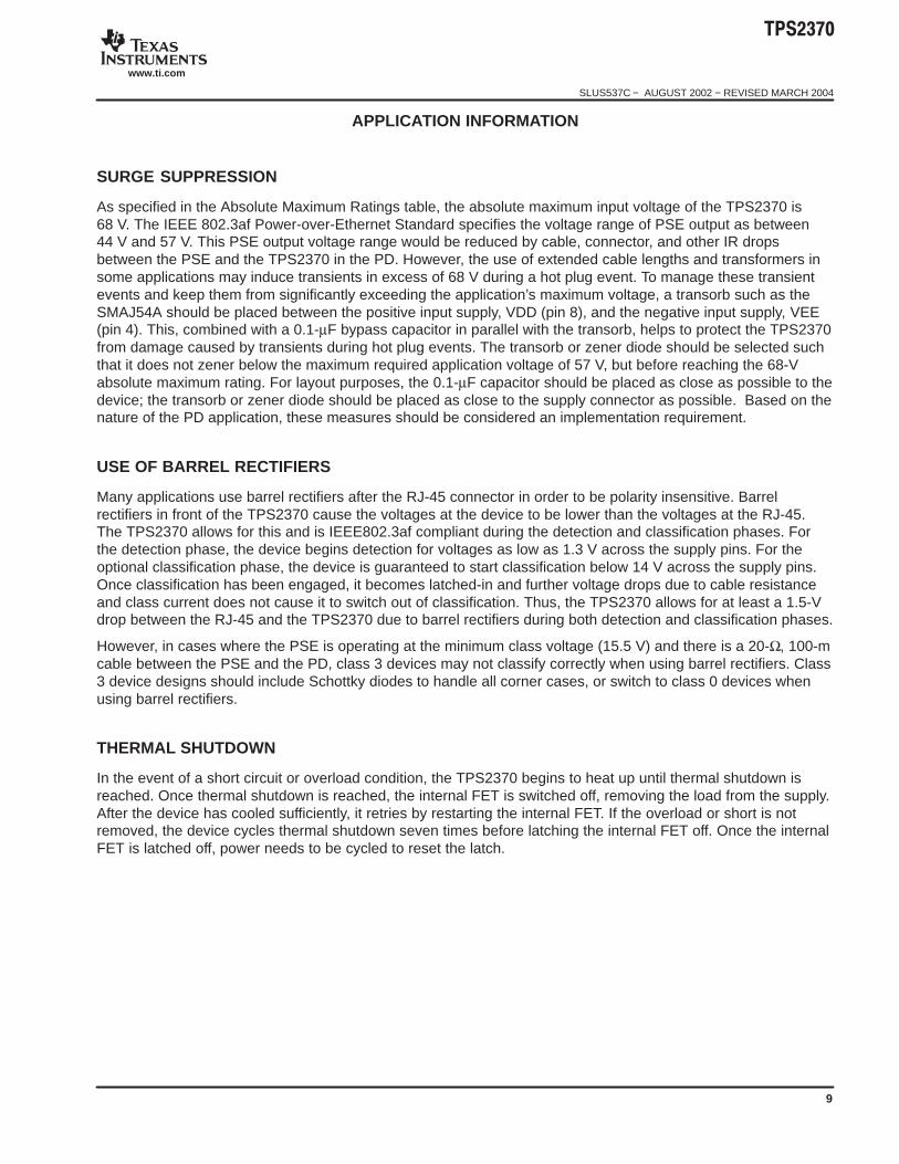
Figure 1 shows an application where 40 V < VIN < 57 V. In this case, the brick supply is greater then 40 V andgoes through TPS2370.
3
1
2
4 5
TPS2370 6 DC/DCCONVERTER
8
ETHERNETDEVICE
VREG
V+
V−
PoE POWERED DEVICE FRONT END
RJ−45
DCBRICK
SUPPLY
3
6
1
2
4
5
7
8
RX
TX
SPARE
RDET
RLIM
CSS
CDCDCIN
RCLASS
Figure 1. For Applications 40 V < V IN < 57 V.
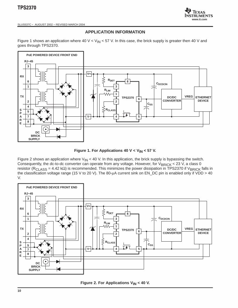
Figure 2 shows an application where VIN < 40 V. In this application, the brick supply is bypassing the switch.Consequently, the dc-to-dc converter can operate from any voltage. However, for VBRICK < 23 V, a class 0resistor (RCLASS = 4.42 kΩ) is recommended. This minimizes the power dissipation in TPS2370 if VBRICK falls inthe classification voltage range (15 V to 20 V). The 80-µA current sink on EN_DC pin is enabled only if VDD > 40V.
RDET
RLIM
CSS
CDCDCIN
RCLASS
3
1
2
4 5
TPS2370 6 DC/DCCONVERTER
8
ETHERNETDEVICE
VREG
V+
V−
PoE POWERED DEVICE FRONT END
RJ−45
DCBRICK
SUPPLY
3
6
1
2
4
578
RX
TX
SPARE
Figure 2. For Applications V IN < 40 V.
PACKAGE OPTION ADDENDUM
www.ti.com 4-Nov-2016
Addendum-Page 1
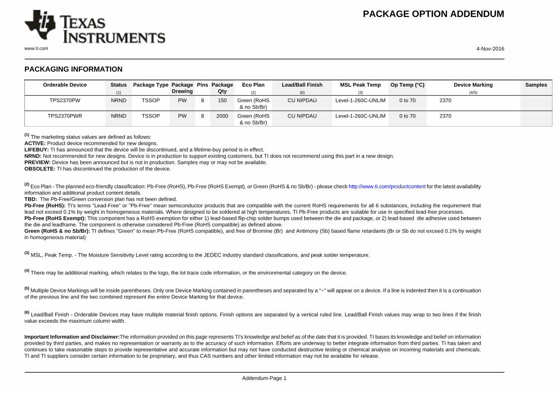
PACKAGING INFORMATION
Orderable Device Status(1)
Package Type PackageDrawing
Pins PackageQty
Eco Plan(2)
Lead/Ball Finish(6)
MSL Peak Temp(3)
Op Temp (°C) Device Marking(4/5)
Samples
TPS2370PW NRND TSSOP PW 8 150 Green (RoHS& no Sb/Br)
CU NIPDAU Level-1-260C-UNLIM 0 to 70 2370
TPS2370PWR NRND TSSOP PW 8 2000 Green (RoHS& no Sb/Br)
CU NIPDAU Level-1-260C-UNLIM 0 to 70 2370
(1) The marketing status values are defined as follows:ACTIVE: Product device recommended for new designs.LIFEBUY: TI has announced that the device will be discontinued, and a lifetime-buy period is in effect.NRND: Not recommended for new designs. Device is in production to support existing customers, but TI does not recommend using this part in a new design.PREVIEW: Device has been announced but is not in production. Samples may or may not be available.OBSOLETE: TI has discontinued the production of the device.
(2) Eco Plan - The planned eco-friendly classification: Pb-Free (RoHS), Pb-Free (RoHS Exempt), or Green (RoHS & no Sb/Br) - please check http://www.ti.com/productcontent for the latest availabilityinformation and additional product content details.TBD: The Pb-Free/Green conversion plan has not been defined.Pb-Free (RoHS): TI's terms "Lead-Free" or "Pb-Free" mean semiconductor products that are compatible with the current RoHS requirements for all 6 substances, including the requirement thatlead not exceed 0.1% by weight in homogeneous materials. Where designed to be soldered at high temperatures, TI Pb-Free products are suitable for use in specified lead-free processes.Pb-Free (RoHS Exempt): This component has a RoHS exemption for either 1) lead-based flip-chip solder bumps used between the die and package, or 2) lead-based die adhesive used betweenthe die and leadframe. The component is otherwise considered Pb-Free (RoHS compatible) as defined above.Green (RoHS & no Sb/Br): TI defines "Green" to mean Pb-Free (RoHS compatible), and free of Bromine (Br) and Antimony (Sb) based flame retardants (Br or Sb do not exceed 0.1% by weightin homogeneous material)
(3) MSL, Peak Temp. - The Moisture Sensitivity Level rating according to the JEDEC industry standard classifications, and peak solder temperature.
(4) There may be additional marking, which relates to the logo, the lot trace code information, or the environmental category on the device.
(5) Multiple Device Markings will be inside parentheses. Only one Device Marking contained in parentheses and separated by a "~" will appear on a device. If a line is indented then it is a continuationof the previous line and the two combined represent the entire Device Marking for that device.
(6) Lead/Ball Finish - Orderable Devices may have multiple material finish options. Finish options are separated by a vertical ruled line. Lead/Ball Finish values may wrap to two lines if the finishvalue exceeds the maximum column width.
Important Information and Disclaimer:The information provided on this page represents TI's knowledge and belief as of the date that it is provided. TI bases its knowledge and belief on informationprovided by third parties, and makes no representation or warranty as to the accuracy of such information. Efforts are underway to better integrate information from third parties. TI has taken andcontinues to take reasonable steps to provide representative and accurate information but may not have conducted destructive testing or chemical analysis on incoming materials and chemicals.TI and TI suppliers consider certain information to be proprietary, and thus CAS numbers and other limited information may not be available for release.
PACKAGE OPTION ADDENDUM
www.ti.com 4-Nov-2016
Addendum-Page 2
In no event shall TI's liability arising out of such information exceed the total purchase price of the TI part(s) at issue in this document sold by TI to Customer on an annual basis.
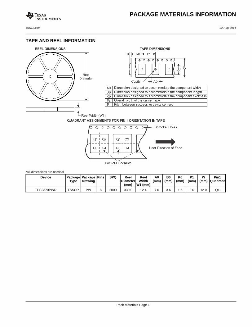
TAPE AND REEL INFORMATION
*All dimensions are nominal
Device PackageType
PackageDrawing
Pins SPQ ReelDiameter
(mm)
ReelWidth
W1 (mm)
A0(mm)
B0(mm)
K0(mm)
P1(mm)
W(mm)
Pin1Quadrant
TPS2370PWR TSSOP PW 8 2000 330.0 12.4 7.0 3.6 1.6 8.0 12.0 Q1
PACKAGE MATERIALS INFORMATION
www.ti.com 10-Aug-2016
Pack Materials-Page 1
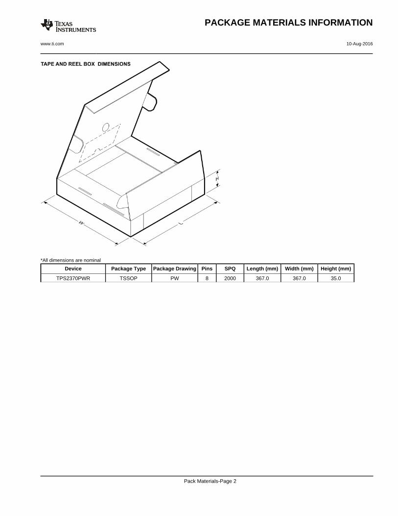
*All dimensions are nominal
Device Package Type Package Drawing Pins SPQ Length (mm) Width (mm) Height (mm)
TPS2370PWR TSSOP PW 8 2000 367.0 367.0 35.0
PACKAGE MATERIALS INFORMATION
www.ti.com 10-Aug-2016
Pack Materials-Page 2
www.ti.com
PACKAGE OUTLINE
C
TYP6.66.2
1.2 MAX
6X 0.65
8X 0.300.19
2X1.95
0.150.05
(0.15) TYP
0 - 8
0.25GAGE PLANE
0.750.50
A
NOTE 3
3.12.9
BNOTE 4
4.54.3
4221848/A 02/2015
TSSOP - 1.2 mm max heightPW0008ASMALL OUTLINE PACKAGE
NOTES: 1. All linear dimensions are in millimeters. Any dimensions in parenthesis are for reference only. Dimensioning and tolerancing per ASME Y14.5M. 2. This drawing is subject to change without notice. 3. This dimension does not include mold flash, protrusions, or gate burrs. Mold flash, protrusions, or gate burrs shall not exceed 0.15 mm per side. 4. This dimension does not include interlead flash. Interlead flash shall not exceed 0.25 mm per side.5. Reference JEDEC registration MO-153, variation AA.
18
0.1 C A B
54
PIN 1 IDAREA
SEATING PLANE
0.1 C
SEE DETAIL A
DETAIL ATYPICAL
SCALE 2.800
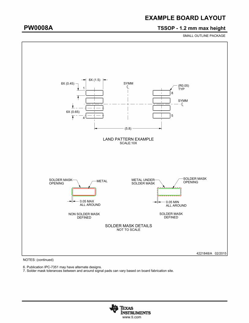
www.ti.com
EXAMPLE BOARD LAYOUT
(5.8)
0.05 MAXALL AROUND
0.05 MINALL AROUND
8X (1.5)8X (0.45)
6X (0.65)
(R )TYP
0.05
4221848/A 02/2015
TSSOP - 1.2 mm max heightPW0008ASMALL OUTLINE PACKAGE
SYMM
SYMM
LAND PATTERN EXAMPLESCALE:10X
1
45
8
NOTES: (continued) 6. Publication IPC-7351 may have alternate designs. 7. Solder mask tolerances between and around signal pads can vary based on board fabrication site.
METALSOLDER MASKOPENING
NON SOLDER MASKDEFINED
SOLDER MASK DETAILSNOT TO SCALE
SOLDER MASKOPENING
METAL UNDERSOLDER MASK
SOLDER MASKDEFINED
www.ti.com
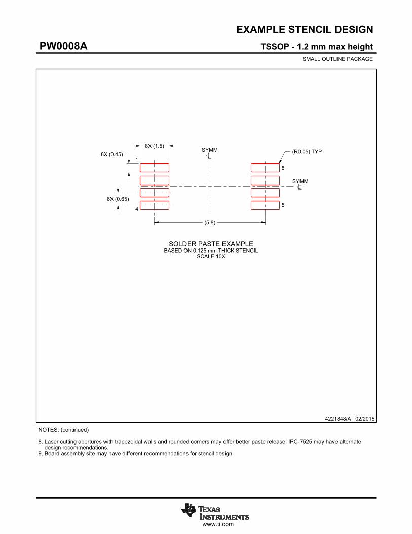
EXAMPLE STENCIL DESIGN
(5.8)
6X (0.65)
8X (0.45)8X (1.5)
(R ) TYP0.05
4221848/A 02/2015
TSSOP - 1.2 mm max heightPW0008ASMALL OUTLINE PACKAGE
NOTES: (continued) 8. Laser cutting apertures with trapezoidal walls and rounded corners may offer better paste release. IPC-7525 may have alternate design recommendations. 9. Board assembly site may have different recommendations for stencil design.
SYMM
SYMM
1
45
8
SOLDER PASTE EXAMPLEBASED ON 0.125 mm THICK STENCIL
SCALE:10X
IMPORTANT NOTICE
Texas Instruments Incorporated (TI) reserves the right to make corrections, enhancements, improvements and other changes to itssemiconductor products and services per JESD46, latest issue, and to discontinue any product or service per JESD48, latest issue. Buyersshould obtain the latest relevant information before placing orders and should verify that such information is current and complete.TI’s published terms of sale for semiconductor products (http://www.ti.com/sc/docs/stdterms.htm) apply to the sale of packaged integratedcircuit products that TI has qualified and released to market. Additional terms may apply to the use or sale of other types of TI products andservices.Reproduction of significant portions of TI information in TI data sheets is permissible only if reproduction is without alteration and isaccompanied by all associated warranties, conditions, limitations, and notices. TI is not responsible or liable for such reproduceddocumentation. Information of third parties may be subject to additional restrictions. Resale of TI products or services with statementsdifferent from or beyond the parameters stated by TI for that product or service voids all express and any implied warranties for theassociated TI product or service and is an unfair and deceptive business practice. TI is not responsible or liable for any such statements.Buyers and others who are developing systems that incorporate TI products (collectively, “Designers”) understand and agree that Designersremain responsible for using their independent analysis, evaluation and judgment in designing their applications and that Designers havefull and exclusive responsibility to assure the safety of Designers' applications and compliance of their applications (and of all TI productsused in or for Designers’ applications) with all applicable regulations, laws and other applicable requirements. Designer represents that, withrespect to their applications, Designer has all the necessary expertise to create and implement safeguards that (1) anticipate dangerousconsequences of failures, (2) monitor failures and their consequences, and (3) lessen the likelihood of failures that might cause harm andtake appropriate actions. Designer agrees that prior to using or distributing any applications that include TI products, Designer willthoroughly test such applications and the functionality of such TI products as used in such applications.TI’s provision of technical, application or other design advice, quality characterization, reliability data or other services or information,including, but not limited to, reference designs and materials relating to evaluation modules, (collectively, “TI Resources”) are intended toassist designers who are developing applications that incorporate TI products; by downloading, accessing or using TI Resources in anyway, Designer (individually or, if Designer is acting on behalf of a company, Designer’s company) agrees to use any particular TI Resourcesolely for this purpose and subject to the terms of this Notice.TI’s provision of TI Resources does not expand or otherwise alter TI’s applicable published warranties or warranty disclaimers for TIproducts, and no additional obligations or liabilities arise from TI providing such TI Resources. TI reserves the right to make corrections,enhancements, improvements and other changes to its TI Resources. TI has not conducted any testing other than that specificallydescribed in the published documentation for a particular TI Resource.Designer is authorized to use, copy and modify any individual TI Resource only in connection with the development of applications thatinclude the TI product(s) identified in such TI Resource. NO OTHER LICENSE, EXPRESS OR IMPLIED, BY ESTOPPEL OR OTHERWISETO ANY OTHER TI INTELLECTUAL PROPERTY RIGHT, AND NO LICENSE TO ANY TECHNOLOGY OR INTELLECTUAL PROPERTYRIGHT OF TI OR ANY THIRD PARTY IS GRANTED HEREIN, including but not limited to any patent right, copyright, mask work right, orother intellectual property right relating to any combination, machine, or process in which TI products or services are used. Informationregarding or referencing third-party products or services does not constitute a license to use such products or services, or a warranty orendorsement thereof. Use of TI Resources may require a license from a third party under the patents or other intellectual property of thethird party, or a license from TI under the patents or other intellectual property of TI.TI RESOURCES ARE PROVIDED “AS IS” AND WITH ALL FAULTS. TI DISCLAIMS ALL OTHER WARRANTIES ORREPRESENTATIONS, EXPRESS OR IMPLIED, REGARDING RESOURCES OR USE THEREOF, INCLUDING BUT NOT LIMITED TOACCURACY OR COMPLETENESS, TITLE, ANY EPIDEMIC FAILURE WARRANTY AND ANY IMPLIED WARRANTIES OFMERCHANTABILITY, FITNESS FOR A PARTICULAR PURPOSE, AND NON-INFRINGEMENT OF ANY THIRD PARTY INTELLECTUALPROPERTY RIGHTS. TI SHALL NOT BE LIABLE FOR AND SHALL NOT DEFEND OR INDEMNIFY DESIGNER AGAINST ANY CLAIM,INCLUDING BUT NOT LIMITED TO ANY INFRINGEMENT CLAIM THAT RELATES TO OR IS BASED ON ANY COMBINATION OFPRODUCTS EVEN IF DESCRIBED IN TI RESOURCES OR OTHERWISE. IN NO EVENT SHALL TI BE LIABLE FOR ANY ACTUAL,DIRECT, SPECIAL, COLLATERAL, INDIRECT, PUNITIVE, INCIDENTAL, CONSEQUENTIAL OR EXEMPLARY DAMAGES INCONNECTION WITH OR ARISING OUT OF TI RESOURCES OR USE THEREOF, AND REGARDLESS OF WHETHER TI HAS BEENADVISED OF THE POSSIBILITY OF SUCH DAMAGES.Unless TI has explicitly designated an individual product as meeting the requirements of a particular industry standard (e.g., ISO/TS 16949and ISO 26262), TI is not responsible for any failure to meet such industry standard requirements.Where TI specifically promotes products as facilitating functional safety or as compliant with industry functional safety standards, suchproducts are intended to help enable customers to design and create their own applications that meet applicable functional safety standardsand requirements. Using products in an application does not by itself establish any safety features in the application. Designers mustensure compliance with safety-related requirements and standards applicable to their applications. Designer may not use any TI products inlife-critical medical equipment unless authorized officers of the parties have executed a special contract specifically governing such use.Life-critical medical equipment is medical equipment where failure of such equipment would cause serious bodily injury or death (e.g., lifesupport, pacemakers, defibrillators, heart pumps, neurostimulators, and implantables). Such equipment includes, without limitation, allmedical devices identified by the U.S. Food and Drug Administration as Class III devices and equivalent classifications outside the U.S.TI may expressly designate certain products as completing a particular qualification (e.g., Q100, Military Grade, or Enhanced Product).Designers agree that it has the necessary expertise to select the product with the appropriate qualification designation for their applicationsand that proper product selection is at Designers’ own risk. Designers are solely responsible for compliance with all legal and regulatoryrequirements in connection with such selection.Designer will fully indemnify TI and its representatives against any damages, costs, losses, and/or liabilities arising out of Designer’s non-compliance with the terms and provisions of this Notice.
Mailing Address: Texas Instruments, Post Office Box 655303, Dallas, Texas 75265Copyright © 2017, Texas Instruments Incorporated