smps primary i.c. - especmonitor.espec.ws/files/viper100_841.pdf · -0.3 to 620 -0.3 to 700 v v id...
TRANSCRIPT
March 2002 1/23
VIPer100/SP- VIPer100A/ASP
SMPS PRIMARY I.C.
1
ADJUSTABLE SWITCHING FREQUENCY UPTO 200 kHz
CURRENT MODE CONTROL SOFT START AND SHUT DOWN CONTROL AUTOMATIC BURST MODE OPERATION IN
STAND-BY CONDITION ABLE TO MEET“BLUE ANGEL” NORM (<1w TOTAL POWERCONSUMPTION)
INTERNALLY TRIMMED ZENER REFERENCE UNDERVOLTAGE LOCK-OUT WITH
HYSTERESIS INTEGRATED START-UP SUPPLY AVALANCHE RUGGED OVERTEMPERATURE PROTECTION LOW STAND-BY CURRENT ADJUSTABLE CURRENT LIMITATION
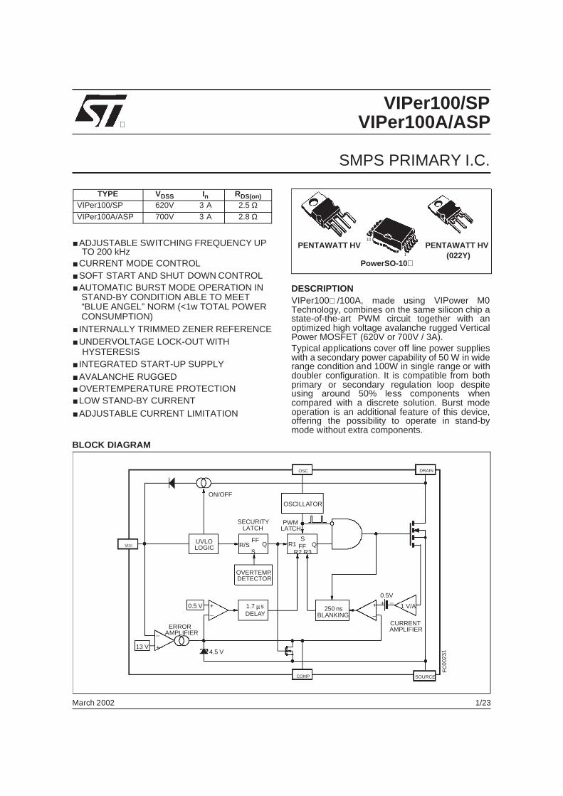
DESCRIPTIONVIPer100 /100A, made using VIPower M0Technology, combines on the same silicon chip astate-of-the-art PWM circuit together with anoptimized high voltage avalanche rugged VerticalPower MOSFET (620V or 700V / 3A).Typical applications cover off line power supplieswith a secondary power capability of 50 W in widerange condition and 100W in single range or withdoubler configuration. It is compatible from bothprimary or secondary regulation loop despiteusing around 50% less components whencompared with a discrete solution. Burst modeoperation is an additional feature of this device,offering the possibility to operate in stand-bymode without extra components.
TYPE VDSS In RDS(on)VIPer100/SP 620V 3 A 2.5 ΩVIPer100A/ASP 700V 3 A 2.8 Ω
BLOCK DIAGRAM
PENTAWATT HV PENTAWATT HV1
10
PowerSO-10 (022Y)
FC
0023
1
VDD
OSC
COMP
DRAIN
SOURCE
13 V
UVLOLOGIC
SECURITYLATCH
PWMLATCH
FFFF
R/SS
QS
R1R2 R3
Q
OSCILLATOR
OVERTEMP.DETECTOR
ERRORAMPLIFIER_
+
0.5 V +_
1.7 µ sDELAY
250 nsBLANKING
CURRENTAMPLIFIER
ON/OFF
0.5V
1 V/A_++
_
4.5 V
2/23
VIPer100/SP - VIPer100A/ASP
ABSOLUTE MAXIMUM RATING
THERMAL DATA
(*) When mounted using the minimum recommended pad size on FR-4 board.
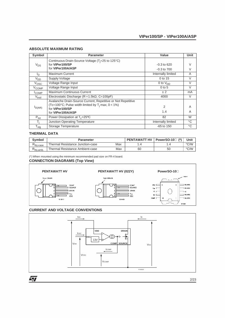
CONNECTION DIAGRAMS (Top View)
CURRENT AND VOLTAGE CONVENTIONS
Symbol Parameter Value Unit
VDS
Continuous Drain-Source Voltage (Tj=25 to 125°C)for VIPer100/SPfor VIPer100A/ASP
-0.3 to 620
-0.3 to 700
V
VID Maximum Current Internally limited A
VDD Supply Voltage 0 to 15 VVOSC Voltage Range Input 0 to VDD V
VCOMP Voltage Range Input 0 to 5 V
ICOMP Maximum Continuous Current ± 2 mAVesd Electrostatic Discharge (R =1.5kΩ; C=100pF) 4000 V
ID(AR)
Avalanche Drain-Source Current, Repetitive or Not Repetitive(Tc=100°C; Pulse width limited by Tj max; δ < 1%)for VIPer100/SPfor VIPer100A/ASP
2
1.4
A
A
Ptot Power Dissipation at Tc=25ºC 82 W
Tj Junction Operating Temperature Internally limited °CTstg Storage Temperature -65 to 150 °C
Symbol Parameter PENTAWATT HV PowerSO-10 (*) UnitRthj-case Thermal Resistance Junction-case Max 1.4 1.4 °C/W
Rthj-amb. Thermal Resistance Ambient-case Max 60 50 °C/W
1
PENTAWATT HV PENTAWATT HV (022Y) PowerSO-10
-
+13VOSC
COMP SOURCE
DRAINVDD
VCOMP
VOSC
VDD VDS
ICOMP
IOSC
IDD ID
FC00020
VIPer100/SP - VIPer100A/ASP
3/23
ORDERING NUMBERS
PINS FUNCTIONAL DESCRIPTION
DRAIN PIN:
Integrated Power MOSFET drain pin. It providesinternal bias current during start-up via anintegrated high voltage current source which isswitched off during normal operation. The deviceis able to handle an unclamped current during itsnormal operation, assuring self protection againstvoltage surges, PCB stray inductance, andallowing a snubberless operation for low outputpower.
SOURCE Pin:
Power MOSFET source pin. Primary side circuitcommon ground connection.
VDD Pin:
This pin provides two functions :
- It corresponds to the low voltage supply of thecontrol part of the circuit. If VDD goes below 8V,the start-up current source is activated and theoutput power MOSFET is switched off until theVDD voltage reaches 11V. During this phase,the internal current consumption is reduced,the VDD pin is sourcing a current of about 2mAand the COMP pin is shorted to ground. Afterthat, the current source is shut down, and thedevice tries to start up by switching again.
- This pin is also connected to the error amplifier,in order to allow primary as well as secondaryregulation configurations. In case of primaryregulation, an internal 13V trimmed referencevoltage is used to maintain VDD at 13V. Forsecondary regulation, a voltage between 8.5Vand 12.5V will be put on VDD pin by transformerdesign, in order to stuck the output of thetransconductance amplifier to the high state.The COMP pin behaves as a constant current
source, and can easily be connected to theoutput of an optocoupler. Note that anyovervoltage due to regulation loop failure is stilldetected by the error amplifier through the VDDvoltage, which cannot overpass 13V. Theoutput voltage will be somewhat higher than thenominal one, but still under control.
COMP PIN:
This pin provides two functions :
- It is the output of the error transconductanceamplifier, and allows for the connection of acompensation network to provide the desiredtransfer function of the regulation loop. Itsbandwidth can be easily adjusted to theneeded value with usual components value. Asstated above, secondary regulationconfigurations are also implemented throughthe COMP pin.
- When the COMP voltage is going below 0.5V,the shut-down of the circuit occurs, with a zeroduty cycle for the power MOSFET. This featurecan be used to switch off the converter, and isautomatically activated by the regulation loop(whatever is the configuration) to provide aburst mode operation in case of negligibleoutput power or open load condition.
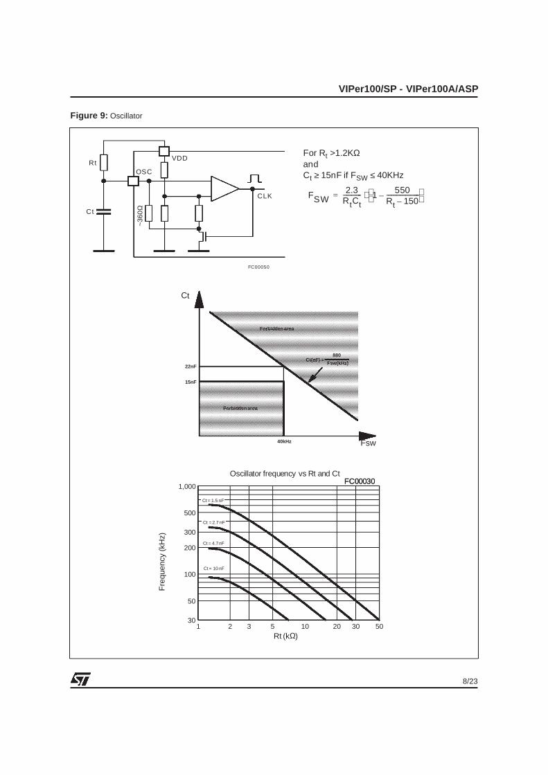
OSC PIN:
An Rt-Ct network must be connected on that pin todefine the switching frequency. Note that despitethe connection of Rt to VDD, no significantfrequency change occurs for VDD varying from 8Vto 15V. It provides also a synchronisationcapability, when connected to an externalfrequency source.
PENTAWATT HV PENTAWATT HV (022Y) PowerSO-10 VIPer100
VIPer100A
VIPer100 (022Y)
VIPer100A (022Y)
VIPer100SP
VIPer100ASP
1

4/23
VIPer100/SP - VIPer100A/ASP
AVALANCHE CHARACTERISTICS
ELECTRICAL CHARACTERISTICS (Tj=25°C; VDD=13V, unless otherwise specified)POWER SECTION
(1) On Inductive Load, Clamped.
SUPPLY SECTION
Symbol Parameter Max Value Unit
ID(AR)
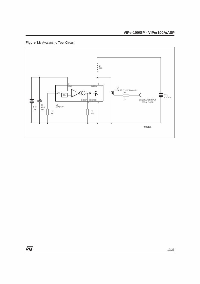
Avalanche Current, Repetitive or Not Repetitive(pulse widht limited by Tj max; δ < 1%)for VIPer100/SPfor VIPer100A/ASP (see fig.12)
2
1.4
A
A
E(AR)Single Pulse Avalanche Energy(starting Tj =25ºC, ID=ID(ar)) (see fig.12)
60 mJ
Symbol Parameter Test Conditions Min Typ Max Unit
BVDSS Drain-Source VoltageID=1mA; VCOMP=0Vfor VIPer100/SPfor VIPer100A/ASP (see fig.5)
620
700
V
V
IDSS Off-State Drain CurrentVCOMP=0V; Tj=125°CVDS=620V for VIPer100/SPVDS=700V for VIPer100A/ASP
1
1
mA
mA
RDS(on)Static Drain-SourceOn Resistance
ID=2Afor VIPer100/SPfor VIPer100A/ASPID=2A; Tj=100°Cfor VIPer100/SPfor VIPer100A/ASP
2.0
2.3
2.5
2.8
4.5
5.0
ΩΩ
ΩΩ
tf Fall TimeID=0.2A; VIN=300V (1)(See fig. 3)
100 ns
tr Rise TimeID=0.4A; VIN=300V (1)(See fig. 3)
50 ns
Coss Output Capacitance VDS=25V 150 pF
Symbol Parameter Test Conditions Min Typ Max Unit
IDDchStart-Up ChargingCurrent
VDD=5V; VDS=35V(see fig. 2 and fig. 15)
-2 mA
IDD0Operating Supply Current VDD=12V; FSW=0kHz
(see fig. 2)12 16 mA
IDD1 Operating Supply Current VDD=12V; Fsw=100kHz 15.5 mAIDD2 Operating Supply Current VDD=12V; Fsw=200kHz 19 mA
VDDoff Undervoltage Shutdown (See fig. 2) 7.5 8 9 VVDDon Undervoltage Reset (See fig. 2) 11 12 V
VDDhyst Hysteresis Start-up (See fig. 2) 2.4 3 V
VIPer100/SP - VIPer100A/ASP
5/23
ELECTRICAL CHARACTERISTICS (continued)OSCILLATOR SECTION
ERROR AMPLIFIER SECTION
PWM COMPARATOR SECTION
SHUTDOWN AND OVERTEMPERATURE SECTION
Symbol Parameter Test Conditions Min Typ Max Unit
FSWOscillator FrequencyTotal Variation
RT=8.2KΩ; CT=2.4nFVDD=9 to 15V;with RT± 1%; CT± 5%(see fig. 6 and fig. 9)
90 100 110 kHz
VOSCIH Oscillator Peak Voltage 7.1 V
VOSCIL Oscillator Valley Voltage 3.7 V
Symbol Parameter Test Conditions Min Typ Max UnitVDDREG VDD Regulation Point ICOMP=0mA (see fig. 1) 12.6 13 13.4 V
∆VDDreg Total Variation Tj=0 to 100°C 2 %
GBW Unity Gain BandwidthFrom Input =VDD to Output = VCOMPCOMP pin is open (see fig. 10)
150 kHz
AVOL Open Loop Voltage Gain COMP pin is open (see fig. 10) 45 52 dBGm DC Transconductance VCOMP=2.5V (see fig. 1) 1.1 1.5 1.9 mA/V
VCOMPLO Output Low Level ICOMP=-400µA; VDD=14V 0.2 V
VCOMPHI Output High Level ICOMP=400µA; VDD=12V 4.5 V
ICOMPLOOutput Low CurrentCapability
VCOMP=2.5V; VDD=14V -600 µA
ICOMPHIOutput High CurrentCapability
VCOMP=2.5V; VDD=12V 600 µA
Symbol Parameter Test Conditions Min Typ Max UnitHID ∆VCOMP / ∆IDPEAK VCOMP=1 to 3 V 0.7 1 1.3 V/A
VCOMPoff VCOMP Offset IDPEAK=10mA 0.5 VIDpeak Peak Current Limitation VDD=12V; COMP pin open 3 4 5.3 A
tdCurrent Sense Delay toTurn-Off
ID=1A 250 ns
tb Blanking Time 250 360 nston(min) Minimum On Time 350 ns
Symbol Parameter Test Conditions Min Typ Max UnitVCOMPth Restart Threshold (see fig. 4) 0.5 V
tDISsu Disable Set Up Time (see fig. 4) 1.7 5 µs
TtsdThermal ShutdownTemperature
(See fig. 8) 140 170 °C
ThystThermal ShutdownHysteresis
(See fig. 8) 40 °C
6/23
VIPer100/SP - VIPer100A/ASP
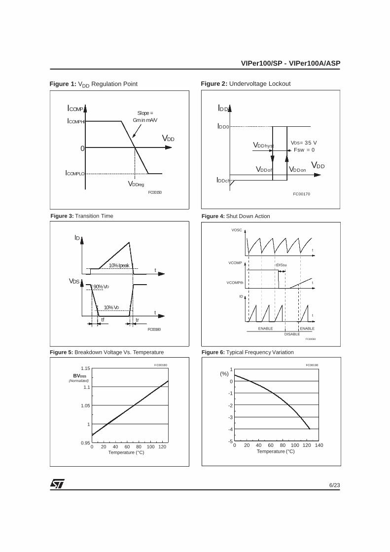
Figure 3: Transition Time Figure 4: Shut Down Action
Figure 5: Breakdown Voltage Vs. Temperature Figure 6: Typical Frequency Variation
Figure 1: VDD Regulation Point Figure 2: Undervoltage Lockout
ICOMP
ICOMPHI
ICOMPLO
VDDreg
0VDD
Slope =Gmin mA/V
FC00150
VDDon
IDDch
IDD0
VDDVDDoff
VDS= 35 VFsw = 0
IDD
VDDhyst
FC00170
ID
VDS
t
ttf tr
10%Ipeak
10%VD
90%VD
FC00160
VCOMP
VOSC
ID
t
tDISsu
t
t
ENABLE
DISABLE
ENABLE
VCOMPth
FC00060
Temperature (°C)
FC00180
0 20 40 60 80 100 1200.95
1
1.05
1.1
1.15
BVDSS(Normalized)
Temperature (°C)0 20 40 60 80 100 120 140
-5
-4
-3
-2
-1
0
1FC00190
(%)
VIPer100/SP - VIPer100A/ASP
7/23
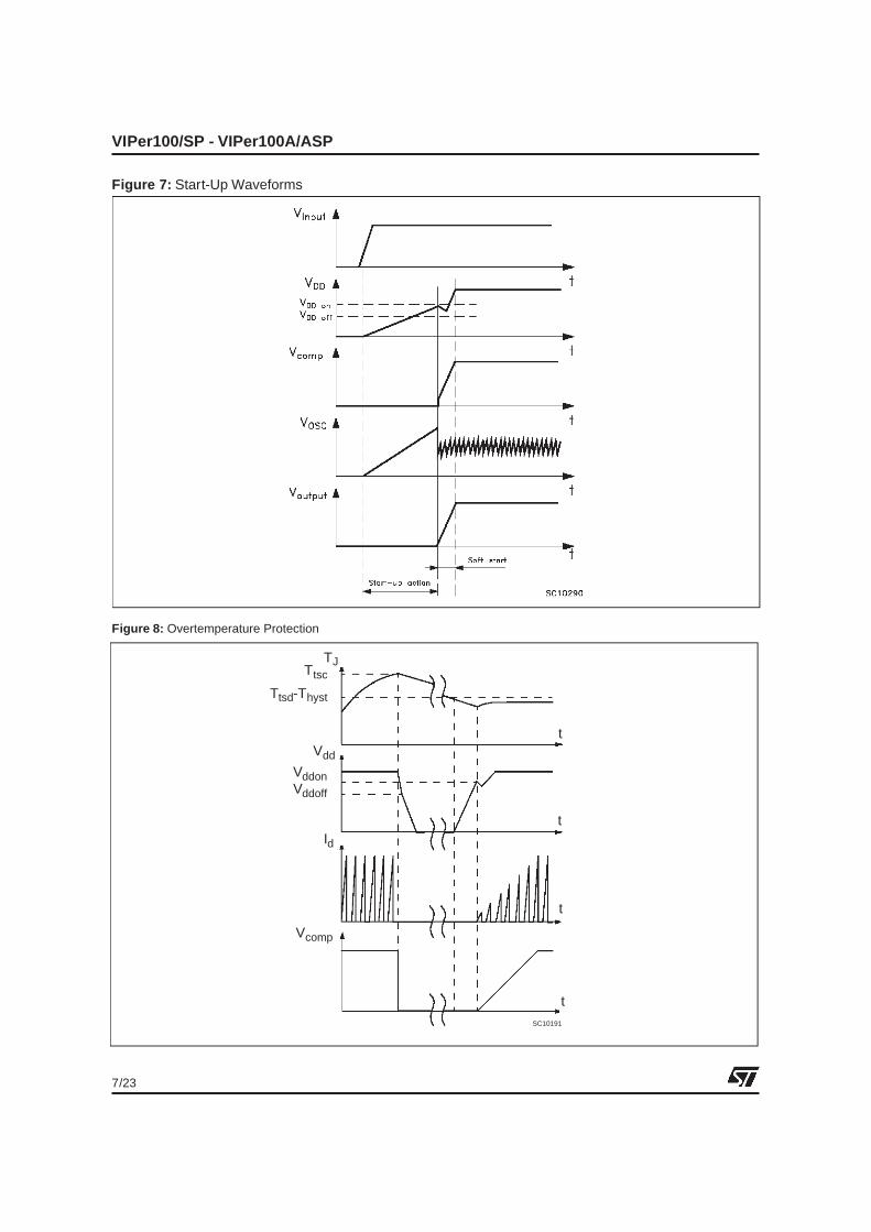
Figure 7: Start-Up Waveforms
Figure 8: Overtemperature Protection
SC10191
TJ
Ttsd-Thyst
Ttsc
Vdd
VddonVddoff
Id
Vcomp
t
t
t
t
8/23
VIPer100/SP - VIPer100A/ASP
Figure 9: Oscillator
1
Rt
Ct
OSC
VDD
~36
0Ω
CLK
FC00050
1 2 3 5 10 20 30 5030
50
100
200
300
500
1,000
Rt (kΩ)
Fre
quen
cy(k
Hz)
Oscillator frequency vs Rt and Ct
Ct = 1.5 nF
Ct =2.7 nF
Ct = 4.7nF
Ct = 10 nF
FC00030FC00030
For Rt >1.2KΩandCt ≥ 15nF if FSW ≤ 40KHz
FSW2.3
RtCt------------ 1 550
Rt 150–----------------------–
⋅=
Ct
Fsw40kHz
15nF
22nF
Forbiddenarea
Forbiddenarea
Ct(nF) =Fsw(kHz)
880
VIPer100/SP - VIPer100A/ASP
9/23
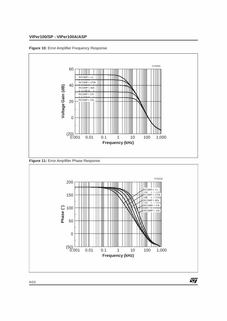
Figure 10: Error Amplifier Frequency Response
Figure 11: Error Amplifier Phase Response
1
0.001 0.01 0.1 1 10 100 1,000(20)
0
20
40
60
Frequency (kHz)
Vol
tage
Gai
n(d
B)
RCOMP = +∞
RCOMP = 270k
RCOMP = 82k
RCOMP = 27k
RCOMP = 12k
FC00200
0.001 0.01 0.1 1 10 100 1,000(50)
0
50
100
150
200
Frequency (kHz)
Pha
se(°
)
RCOMP = +∞
RCOMP = 270k
RCOMP = 82k
RCOMP = 27k
RCOMP = 12k
FC00210
10/23
VIPer100/SP - VIPer100A/ASP
Figure 12: Avalanche Test Circuit
1
FC00195
U1VIPer100
13VOSC
COMP SOURCE
DRAINVDD
-
+
2 3
5 4
1
R3
100
R2
1k
BT212V
C147uF16V
Q12 x STHV102FI in parallel
R1
47
L11mH
GENERATOR INPUT500us PULSE
BT10 to 20V
11/23
VIPer100/SP - VIPer100A/ASP
1
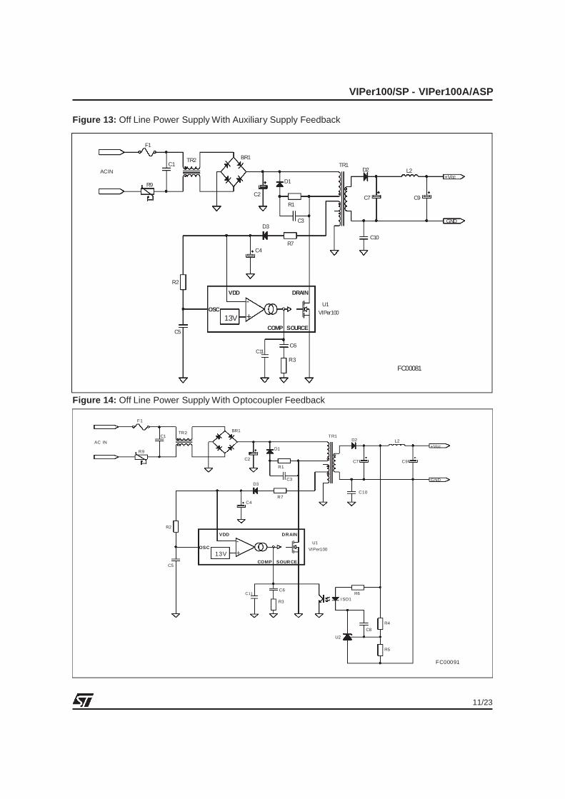
Figure 13: Off Line Power Supply With Auxiliary Supply Feedback
Figure 14: Off Line Power Supply With Optocoupler Feedback
ACIN+Vcc
GND
F1
BR1
D3
R9
C1
R7C4
C2
TR2
R1
C3
D1
D2
C10
TR1
C9C7
L2
R3
C6
C5
R2
U1VIPer100
-
+13VOSC
COMP SOURCE
DRAINVDD
FC00081
C11
FC00091
AC IN
F1
BR1
D3
R9
C1
R7C4
C2
TR2
R1
C3
D1
D2
C10
TR1
C9C7
L2+Vcc
GND
C8
C5
R2
U1
VIPer100
U2
R4
R5
ISO1R6
R3
C6
-
+13VOSC
COMP SOURCE
DRAINVDD
C11
12/23
VIPer100/SP - VIPer100A/ASP
OPERATION DESCRIPTION:
CURRENT MODE TOPOLOGY:The current mode control method, like the oneintegrated in the VIPer100/100A uses two controlloops - an inner current control loop and an outerloop for voltage control. When the PowerMOSFET output transistor is on, the inductorcurrent (primary side of the transformer) ismonitored with a SenseFET technique andconverted into a voltage VS proportional to thiscurrent. When VS reaches VCOMP (the amplifiedoutput voltage error) the power switch is switchedoff. Thus, the outer voltage control loop definesthe level at which the inner loop regulates peakcurrent through the power switch and the primarywinding of the transformer.
Excellent open loop D.C. and dynamic lineregulation is ensured due to the inherent inputvoltage feedforward characteristic of the currentmode control. This results in an improved lineregulation, instantaneous correction to linechanges and better stability for the voltageregulation loop.Current mode topology also ensures goodlimitation in the case of short circuit. During a firstphase the output current increases slowlyfollowing the dynamic of the regulation loop. Thenit reaches the maximum limitation currentinternally set and finally stops because the powersupply on VDD is no longer correct. For specificapplications the maximum peak current internallyset can be overridden by externally limiting thevoltage excursion on the COMP pin. An integratedblanking filter inhibits the PWM comparator outputfor a short time after the integrated PowerMOSFET is switched on. This function preventsanomalous or premature termination of theswitching pulse in the case of current spikescaused by primary side capacitance or secondaryside rectifier reverse recovery time.
STAND-BY MODEStand-by operation in nearly open load conditionautomatically leads to a burst mode operationallowing voltage regulation on the secondary side.The transition from normal operation to burstmode operation happens for a power PSTBY givenby :
Where:
LP is the primary inductance of the transformer.
FSW is the normal switching frequency.
ISTBY is the minimum controllable current,corresponding to the minimum on time that thedevice is able to provide in normal operation. Thiscurrent can be computed as :
tb + td is the sum of the blanking time and of thepropagation time of the internal current sense andcomparator, and represents roughly the minimumon time of the device. Note that PSTBY may beaffected by the efficiency of the converter at lowload, and must include the power drawn on theprimary auxiliary voltage.As soon as the power goes below this limit, theauxiliary secondary voltage starts to increaseabove the 13V regulation level forcing the outputvoltage of the transconductance amplifier to lowstate (VCOMP < VCOMPth). This situation leads tothe shutdown mode where the power switch ismaintained in the off state, resulting in missingcycles and zero duty cycle. As soon as VDD getsback to the regulation level and the VCOMPththreshold is reached, the device operates again.The above cycle repeats indefinitely, providing aburst mode of which the effective duty cycle ismuch lower than the minimum one when in normaloperation. The equivalent switching frequency isalso lower than the normal one, leading to areduced consumption on the input mains lines.This mode of operation allows the VIPer100/100Ato meet the new German ”Blue Angel” Norm withless than 1W total power consumption for thesystem when working in stand-by. The outputvoltage remains regulated around the normallevel, with a low frequency ripple corresponding tothe burst mode. The amplitude of this ripple is low,because of the output capacitors and of the lowoutput current drawn in such conditions.Thenormal operation resumes automatically when thepower get back to higher levels than PSTBY.
HIGH VOLTAGE START-UP CURRENTSOURCEAn integrated high voltage current source providesa bias current from the DRAIN pin during the start-up phase. This current is partially absorbed byinternal control circuits which are placed into astandby mode with reduced consumption and alsoprovided to the external capacitor connected to theVDD pin. As soon as the voltage on this pinreaches the high voltage threshold VDDon of theUVLO logic, the device turns into active mode andstarts switching.
PSTBY12---LPI
2STBYFSW=
ISTBY
tb td+( )VINLP
--------------------------------=
13/23
VIPer100/SP - VIPer100A/ASP
The start up current generator is switched off, andthe converter should normally provide the neededcurrent on the VDD pin through the auxiliarywinding of the transformer, as shown on figure 15.
In case of abnormal condition where the auxiliarywinding is unable to provide the low voltage supplycurrent to the VDD pin (i.e. short circuit on theoutput of the converter), the external capacitordischarges itself down to the low threshold voltageVDDoff of the UVLO logic, and the device get backto the inactive state where the internal circuits arein standby mode and the start up current source isactivated. The converter enters a endless start upcycle, with a start-up duty cycle defined by theratio of charging current towards discharging whenthe VIPer100/100A tries to start. This ratio is fixedby design to 2 to 15, which gives a 12% start upduty cycle while the power dissipation at start up isapproximately 0.6 W, for a 230 Vrms input voltage.This low value of start-up duty cycle prevents thestress of the output rectifiers and of thetransformer when in short circuit.
The external capacitor CVDD on the VDD pin mustbe sized according to the time needed by theconverter to start up, when the device startsswitching. This time tSS depends on manyparameters, among which transformer design,output capacitors, soft start feature andcompensation network implemented on the COMPpin. The following formula can be used for definingthe minimum capacitor needed:
where:
IDD is the consumption current on the VDD pinwhen switching. Refer to specified IDD1 and IDD2values.
tSS is the start up time of the converter when thedevice begins to switch. Worst case is generally atfull load.
VDDhyst is the voltage hysteresis of the UVLOlogic. Refer to the minimum specified value.
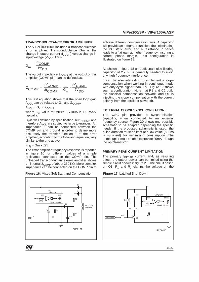
Soft start feature can be implemented on theCOMP pin through a simple capacitor which will bealso used as the compensation network. In thiscase, the regulation loop bandwidth is rather low,because of the large value of this capacitor. Incase a large regulation loop bandwidth ismandatory, the schematics of figure 16 can beused. It mixes a high performance compensationnetwork together with a separate high value softstart capacitor. Both soft start time and regulationloop bandwidth can be adjusted separately.If the device is intentionally shut down by puttingthe COMP pin to ground, the device is alsoperforming start-up cycles, and the VDD voltage isoscillating between VDDon and VDDoff.This voltage can be used for supplying externalfunctions, provided that their consumption doesn’texceed 0.5mA. Figure 17 shows a typicalapplication of this function, with a latched shutdown. Once the ”Shutdown” signal has beenactivated, the device remains in the off state untilthe input voltage is removed.
CVDD
IDDtSSVDDhyst-------------------------->
Figure 15: Behaviour of the high voltage current source at start-up
Ref.
UNDERVOLTAGELOCK OUT LOGIC
15 mA1 mA
3 mA2 mA
15 mA
VDD DRAIN
SOURCEVIPer100
Auxiliary primarywinding
VDD
t
VDDoffVDDon
Start up duty cycle ~ 12%
CVDD
FC00100
14/23
VIPer100/SP - VIPer100A/ASP
TRANSCONDUCTANCE ERROR AMPLIFIERThe VIPer100/100A includes a transconductanceerror amplifier. Transconductance Gm is thechange in output current (ICOMP) versus change ininput voltage (VDD). Thus:
The output impedance ZCOMP at the output of thisamplifier (COMP pin) can be defined as:
This last equation shows that the open loop gainAVOL can be related to Gm and ZCOMP:
AVOL = Gm x ZCOMP
where Gm value for VIPer100/100A is 1.5 mA/Vtypically.
Gmis well defined by specification, but ZCOMP andtherefore AVOL are subject to large tolerances. Animpedance Z can be connected between theCOMP pin and ground in order to define moreaccurately the transfer function F of the erroramplifier, according to the following equation, verysimilar to the one above:
F(S) = Gm x Z(S)
The error amplifier frequency response is reportedin figure 10 for different values of a simpleresistance connected on the COMP pin. Theunloaded transconductance error amplifier showsan internal ZCOMP of about 330 KΩ. More compleximpedance can be connected on the COMP pin to
achieve different compensation laws. A capacitorwill provide an integrator function, thus eliminatingthe DC static error, and a resistance in seriesleads to a flat gain at higher frequency, insuring acorrect phase margin. This configuration isillustrated on figure 18.
As shown in figure 18 an additional noise filteringcapacitor of 2.2 nF is generally needed to avoidany high frequency interference.
It can be also interesting to implement a slopecompensation when working in continuous modewith duty cycle higher than 50%. Figure 19 showssuch a configuration. Note that R1 and C2 buildthe classical compensation network, and Q1 isinjecting the slope compensation with the correctpolarity from the oscillator sawtooth.
EXTERNAL CLOCK SYNCHRONIZATION:The OSC pin provides a synchronisationcapability, when connected to an externalfrequency source. Figure 20 shows one possibleschematic to be adapted depending the specificneeds. If the proposed schematic is used, thepulse duration must be kept at a low value (500nsis sufficient) for minimizing consumption. Theoptocoupler must be able to provide 20mA throughthe optotransistor.
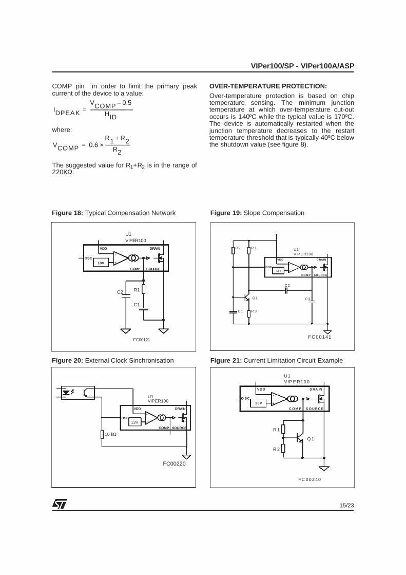
PRIMARY PEAK CURRENT LIMITATIONThe primary IDPEAK current and, as resultingeffect, the output power can be limited using thesimple circuit shown in figure 21. The circuit basedon Q1, R1 and R2 clamps the voltage on the
Gm
∂ICOMP∂VDD
------------------------=
ZCOMP
∂VCOMP∂ICOMP--------------------------- 1
mG---------
∂VCOMP∂VDD
---------------------------×= =
Figure 16: Mixed Soft Start and Compensation Figure 17: Latched Shut Down
AUXILIARYWINDING
-
+13VOSC
COMP SOURCE
DRAINVDD
U1VIPER100
R1
C1 +C2
D1
R2
R3
D2
D3
+ C3
FC00131
C4
-
+13VOSC
COMP SOURCE
DRAINVDD
VIPER100
Shutdown
U1
Q1
Q2
R1
R2R3
R4D1
FC00110
15/23
VIPer100/SP - VIPer100A/ASP
COMP pin in order to limit the primary peakcurrent of the device to a value:
where:
The suggested value for R1+R2 is in the range of220KΩ.
OVER-TEMPERATURE PROTECTION:Over-temperature protection is based on chiptemperature sensing. The minimum junctiontemperature at which over-temperature cut-outoccurs is 140ºC while the typical value is 170ºC.The device is automatically restarted when thejunction temperature decreases to the restarttemperature threshold that is typically 40ºC belowthe shutdown value (see figure 8).
IDPEAK
VCOMP 0.5–
HID-------------------------------------=
VCOMP 0.6R1 R2+
R2----------------------×=
Figure 18: Typical Compensation Network
Figure 20: External Clock Sinchronisation
Figure 19: Slope Compensation
Figure 21: Current Limitation Circuit Example
-
+13VOSC
COMP SOURCE
DRAINVDD
VIPER100U1
R1
C1
FC00121
C2
FC 00141
-
+13VO SC
COM P SO URC E
D RAINVDD
V IP E R100
R 1R2
Q1
C2
C1 R 3
U1
C3
-
+13VOSC
COMP SOURCE
DRAINVDD
U1VIPER100
10 kΩ
FC00220
-
+1 3VO SC
C O M P S O U R C E
D RA INVD D
VIP E R1 0 0U1
R 1
R 2
Q 1
FC 0 0 2 40
16/23
VIPer100/SP - VIPer100A/ASP
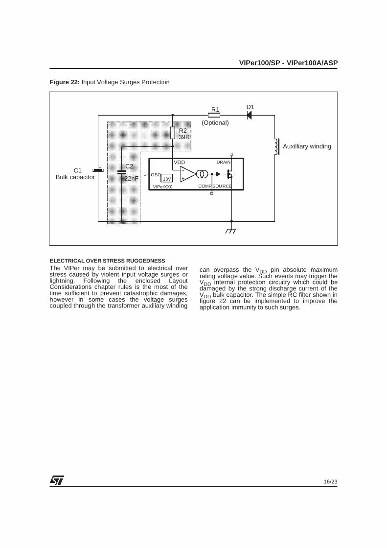
Figure 22: Input Voltage Surges Protection
ELECTRICAL OVER STRESS RUGGEDNESSThe VIPer may be submitted to electrical overstress caused by violent input voltage surges orlightning. Following the enclosed LayoutConsiderations chapter rules is the most of thetime sufficient to prevent catastrophic damages,however in some cases the voltage surgescoupled through the transformer auxiliary winding
can overpass the VDD pin absolute maximumrating voltage value. Such events may trigger theVDD internal protection circuitry which could bedamaged by the strong discharge current of theVDD bulk capacitor. The simple RC filter shown infigure 22 can be implemented to improve theapplication immunity to such surges.
C1Bulk capacitor
D1R1
(Optional)
C2
22nF
Auxilliary winding
13VOSC
COMP SOURCE
DRAINVDD
-
+
VIPerXX0
R239R
17/23
VIPer100/SP - VIPer100A/ASP
1
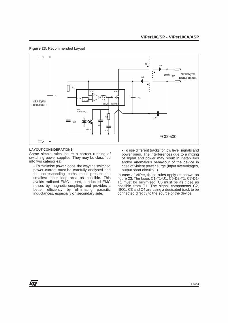
Figure 23: Recommended Layout
LAYOUT CONSIDERATIONSSome simple rules insure a correct running ofswitching power supplies. They may be classifiedinto two categories:
- To minimise power loops: the way the switchedpower current must be carefully analysed andthe corresponding paths must present thesmallest inner loop area as possible. Thisavoids radiated EMC noises, conducted EMCnoises by magnetic coupling, and provides abetter efficiency by eliminating parasiticinductances, especially on secondary side.
- To use different tracks for low level signals andpower ones. The interferences due to a mixingof signal and power may result in instabilitiesand/or anomalous behaviour of the device incase of violent power surge (Input overvoltages,output short circuits...).
In case of VIPer, these rules apply as shown onfigure 23. The loops C1-T1-U1, C5-D2-T1, C7-D1-T1 must be minimised. C6 must be as close aspossible from T1. The signal components C2,ISO1, C3 and C4 are using a dedicated track to beconnected directly to the source of the device.
T1
U1VIPerXX0
13VOSC
COMP SOURCE
DRAINVDD
-
+
C4
C2
C5C1
D2
R1
R2
D1
C7
C6
C3
ISO1
)URP LQSXWGLRGHV EULGJH
7R VHFRQGDU\ILOWHULQJ DQG ORDG
FC00500

18/23
VIPer100/SP - VIPer100A/ASP
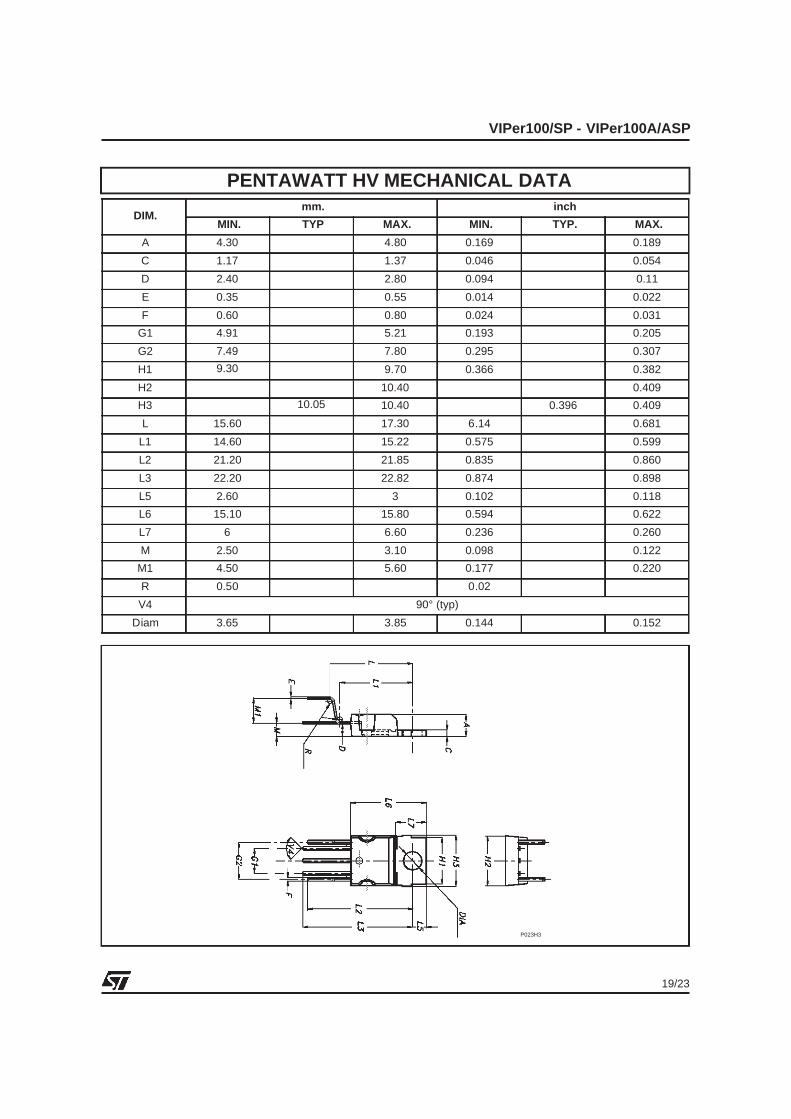
DIM.mm. inch
MIN. TYP MAX. MIN. TYP. MAX.
A 3.35 3.65 0.132 0.144A (*) 3.4 3.6 0.134 0.142A1 0.00 0.10 0.000 0.004B 0.40 0.60 0.016 0.024
B (*) 0.37 0.53 0.014 0.021C 0.35 0.55 0.013 0.022
C (*) 0.23 0.32 0.009 0.0126D 9.40 9.60 0.370 0.378
D1 7.40 7.60 0.291 0.300E 9.30 9.50 0.366 0.374E2 7.20 7.60 0.283 300
E2 (*) 7.30 7.50 0.287 0.295E4 5.90 6.10 0.232 0.240
E4 (*) 5.90 6.30 0.232 0.248e 1.27 0.050F 1.25 1.35 0.049 0.053
F (*) 1.20 1.40 0.047 0.055H 13.80 14.40 0.543 0.567
H (*) 13.85 14.35 0.545 0.565h 0.50 0.002L 1.20 1.80 0.047 0.070
L (*) 0.80 1.10 0.031 0.043α 0º 8º 0º 8º
α (*) 2º 8º 2º 8º
PowerSO-10 MECHANICAL DATA
(*) Muar only POA P013P
DETAIL ”A”
PLANESEATING
α
L
A1F
A1
h
A
D
D1= =
= =
E4
0.10 A
CA
B
B
DETAIL ”A”
SEATINGPLANE
E2
10
1
e B
H E
0.25
P095A
19/23
VIPer100/SP - VIPer100A/ASP
11
DIM.mm. inch
MIN. TYP MAX. MIN. TYP. MAX.
A 4.30 4.80 0.169 0.189
C 1.17 1.37 0.046 0.054
D 2.40 2.80 0.094 0.11
E 0.35 0.55 0.014 0.022
F 0.60 0.80 0.024 0.031
G1 4.91 5.21 0.193 0.205
G2 7.49 7.80 0.295 0.307
H1 9.30 9.70 0.366 0.382
H2 10.40 0.409
H3 10.05 10.40 0.396 0.409
L 15.60 17.30 6.14 0.681
L1 14.60 15.22 0.575 0.599
L2 21.20 21.85 0.835 0.860
L3 22.20 22.82 0.874 0.898
L5 2.60 3 0.102 0.118
L6 15.10 15.80 0.594 0.622
L7 6 6.60 0.236 0.260
M 2.50 3.10 0.098 0.122
M1 4.50 5.60 0.177 0.220
R 0.50 0.02
V4 90° (typ)
Diam 3.65 3.85 0.144 0.152
P023H3
PENTAWATT HV MECHANICAL DATA
20/23
VIPer100/SP - VIPer100A/ASP
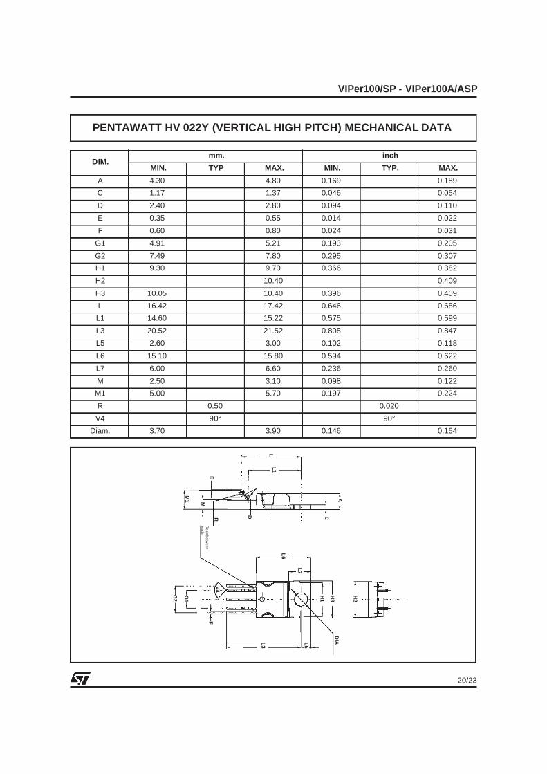
1
A
C
H2
H3
H1
L5
DIAL3
L6
L7
F
G1
G2
LL1
DR
M
M1
ER
esinbetw
eenleads
V4
DIM.mm. inch
MIN. TYP MAX. MIN. TYP. MAX.
A 4.30 4.80 0.169 0.189
C 1.17 1.37 0.046 0.054
D 2.40 2.80 0.094 0.110
E 0.35 0.55 0.014 0.022
F 0.60 0.80 0.024 0.031
G1 4.91 5.21 0.193 0.205
G2 7.49 7.80 0.295 0.307
H1 9.30 9.70 0.366 0.382
H2 10.40 0.409
H3 10.05 10.40 0.396 0.409
L 16.42 17.42 0.646 0.686
L1 14.60 15.22 0.575 0.599
L3 20.52 21.52 0.808 0.847
L5 2.60 3.00 0.102 0.118
L6 15.10 15.80 0.594 0.622
L7 6.00 6.60 0.236 0.260
M 2.50 3.10 0.098 0.122
M1 5.00 5.70 0.197 0.224
R 0.50 0.020
V4 90° 90°Diam. 3.70 3.90 0.146 0.154
PENTAWATT HV 022Y (VERTICAL HIGH PITCH) MECHANICAL DATA
21/23
VIPer100/SP - VIPer100A/ASP
1
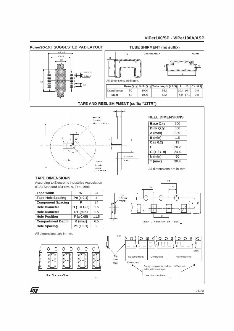
PowerSO-10 SUGGESTED PAD LAYOUT
1
TAPE AND REEL SHIPMENT (suffix “13TR”)
REEL DIMENSIONS
All dimensions are in mm.
Base Q.ty 600Bulk Q.ty 600A (max) 330
B (min) 1.5C (± 0.2) 13F 20.2
G (+ 2 / -0) 24.4N (min) 60T (max) 30.4
TAPE DIMENSIONSAccording to Electronic Industries Association(EIA) Standard 481 rev. A, Feb. 1986
All dimensions are in mm.
Tape width W 24
Tape Hole Spacing P0 ( ± 0.1) 4Component Spacing P 24Hole Diameter D ( ± 0.1/-0) 1.5
Hole Diameter D1 (min) 1.5Hole Position F ( ± 0.05) 11.5Compartment Depth K (max) 6.5
Hole Spacing P1 ( ± 0.1) 2
Topcovertape
End
Start
No componentsNo components Components
500mm min
500mm minEmpty components pocketssaled with cover tape.
User direction of feed
6.30
10.8- 11
14.6-14.9
9.5
1
23
45
1.27
0.67-0.73
0.54-0.6109
8
76
B
A
C
All dimensions are in mm.
Base Q.ty Bulk Q.ty Tube length ( ± 0.5) A B C (± 0.1)
Casablanca 50 1000 532 10.4 16.4 0.8
Muar 50 1000 532 4.9 17.2 0.8
TUBE SHIPMENT (no suffix)
CA
B
MUARCASABLANCA

VIPer100/SP - VIPer100A/ASP
22/23
1
PENTAWATT HV TUBE SHIPMENT (no suffix)
All dimensions are in mm.
Base Q.ty 50Bulk Q.ty 1000Tube length ( ± 0.5) 532A 18B 33.1C (± 0.1) 1C
B
A

VIPer100/SP - VIPer100A/ASP
23/23
1
Information furnished is believed to be accurate and reliable. However, STMicroelectronics assumes no responsibility for the consequencesof use of such information nor for any infringement of patents or other rights of third parties which may results from its use. No license isgranted by implication or otherwise under any patent or patent rights of STMicroelectronics. Specifications mentioned in this publication aresubject to change without notice. This publication supersedes and replaces all information previously supplied. STMicroelectronics productsare not authorized for use as critical components in life support devices or systems without express written approval of STMicroelectronics.
The ST logo is a trademark of STMicroelectronics
2002 STMicroelectronics - Printed in ITALY- All Rights Reserved.
STMicroelectronics GROUP OF COMPANIESAustralia - Brazil - Canada - China - Finland - France - Germany - Hong Kong - India - Israel - Italy - Japan - Malaysia -
Malta - Morocco - Singapore - Spain - Sweden - Switzerland - United Kingdom - U.S.A.
http://www.st.com