slick line acquisition box - · pdf fileto a host windows operating system computer and...
TRANSCRIPT

SCIENTIFIC DATA SYSTEMS, INC.
SLICK LINE ACQUISITION BOX
Slick Line
Acquisition System
Manual
This document contains proprietary information. Copyright © 2005 Scientific Data Systems, Inc. All rights reserved.


2 Slick line Acquisition System - SLAB
SL ICK L INE AQUI S IT ION SYSTEM ( S LAB )
SLAB Manual
This document contains proprietary information.
Copyright © 2005 Scientific Data Systems, Inc. All rights reserved. 16840 Clay Road • Suite 105 Houston, Texas 77084, USA
Phone: 1- 281-550-1109 • Fax: 1- 281-550-2068 E-mail: [email protected] Website: www.warriorsystem.com Created September 11, 2012
Windows® is a registered trademark of Microsoft Corporation in the United States and/or other countries. All other product names are trademarks of their respective companies.

3 Slick Line Acquisition System - SLAB

4 Slick line Acquisition System - SLAB
Table of Contents TABLE OF CONTENTS ........................................................................................................................ 4
1 SLAB HARDWARE ........................................................................................................................... 6
SOFTWARE SETUP AND CONTROLS ...................................................................................................... 6 1.2 USB Control ....................................................................................................................................... 7 1.3 Wellhead Sensors 4 -20 mA. .............................................................................................................. 7 1.4 USB HUB ........................................................................................................................................... 8 1.5 I2C_INIT ............................................................................................................................................ 8 1.6 CCL .................................................................................................................................................... 9 1.7 Well Head Transducers 4-20 mA ....................................................................................................... 9 1.8 Specifications ..................................................................................................................................... 9
2 SLAB CONNECTOR WIRING........................................................................................................... 10
ENCODER CABLE ...................................................................................................................................10 TENSION TRASDUCER CABLE (ASCO PRESSURE TRANSMITER) ..............................................10 12VDC CABLE ..........................................................................................................................................10 2 Pin Female Battery Truck (12 VDC) ...........................................................................................10 WELL HEAD PRESSURE CABLE .........................................................................................................10 FIG: 2.1 SLAB Panel Connections ........................................................................................................11 FIG: 2.2 SLAB STD Wiring Connections ..............................................................................................13 FIG: 2.3 SLAB LWD Wiring Connections .............................................................................................14
3 SLAB MAIN BOARD DESCRIPTION .................................................................................................. 16
MAIN BOARD CIRCUIT DESCRIPTION. .................................................................................................. 16 SLABR3 sheet 1 of 5 ...................................................................................................................................16 SLABR3 sheet 2 of 5 ...................................................................................................................................17 SLABR3 sheet 3 of 5 ...................................................................................................................................17 SLABR3 sheet 4 of 5 ...................................................................................................................................17 SLABR3 sheet 5 of 5 ...................................................................................................................................18 FIG: 3.1 SLAB Schematic 1/5 ................................................................................................................19 FIG: 3.2 SLAB Schematic 2/5 ................................................................................................................20 FIG: 3.3 SLAB Schematic 3/5 ................................................................................................................21 FIG: 3.4 SLAB Schematic 4/5 ................................................................................................................22 FIG: 3.5 SLAB Schematic 5/5 ................................................................................................................23 FIG: 3.6 SLAB Board ............................................................................................................................24
4 SLAB WIRE LIST ............................................................................................................................ 26
CONNECTOR OUTPUTS ...................................................................................................................... 26 Lamp Out CIR-4F .........................................................................................................................................26 Buzzer .........................................................................................................................................................26 S1 AC PWR ..................................................................................................................................................26 S2 AC/DC Switch - DPDT .............................................................................................................................27 F1 AC Fuse ...................................................................................................................................................27 AC IN ...........................................................................................................................................................27 LAMP 12-Red ..............................................................................................................................................27 J3 Well Head Pressure.................................................................................................................................27 4 CCL-BNC ...................................................................................................................................................28
5 Slick Line Acquisition System - SLAB
J5A AUX Outputs LWD ................................................................................................................................ 28 J5 Tension - CIR - 5 - F ................................................................................................................................. 28 J6 Encoder - CIR - 7 - F ................................................................................................................................ 28 J9 Serial D-9 Male ...................................................................................................................................... 28 J10 EXT 12V In ............................................................................................................................................ 28
PCB BOARD CONNECTORS ............................................................................................................... 29 PCB J1 USB In ............................................................................................................................................. 29 PCB J2 CCL In .............................................................................................................................................. 29 PCB J3 INT 12V ........................................................................................................................................... 29 PCB J4 Well head Pressure ......................................................................................................................... 29 PCB J5 Surface tension ............................................................................................................................... 29 PCB J6 Depth .............................................................................................................................................. 29 PCB J7 SGTENS ........................................................................................................................................... 30 PCB J8 SON Buzzer & Lamp ........................................................................................................................ 30 PCB J9 Serial 9 Pin D ................................................................................................................................... 30 PCB J10 Ext 12V .......................................................................................................................................... 30 PCB J11 NC ................................................................................................................................................. 30
6 Slick line Acquisition System - SLAB
1 SLAB Hardware
The Slick Line Acquisition Panel provides a basic logging interface with a USB connection
to a host Windows operating system computer and Warrior Data Acquisition Software.
The panel supports CLL, quadrature depth encoding, tension, and well head pressure
with provision to add additional analog input channels and digital counter channels
through a DB-9 connector, if required. The well head pressure excitation voltage passes
through an MTL safety barrier that limits the voltage to 27 volts and the current to 50
ma. The panel can be powered by 110 VAC, 220 VAC, or 12 volts DC. The supply
voltage for the encoder is software selectable to 5 VDC or 12 VDC. With minor
modifications, the panel can also be used as a Logging While Drilling (LWD) Box. The
panel dimensions are 12” x 12” x 1.75”. Additional space is required for the connectors
on three sides of the box.
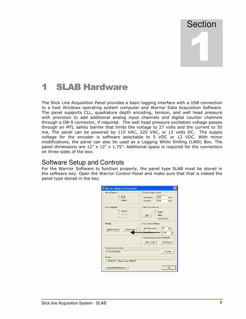
Software Setup and Controls For the Warrior Software to function properly, the panel type SLAB must be stored in
the software key. Open the Warrior Control Panel and make sure that that is indeed the
panel type stored in the key.
Section
1

7 Slick Line Acquisition System - SLAB
The acquisition board in the SLAB must also be properly configured. From acquisition,
select the SLAB service. Once the service has loaded, click on Edit -> Device
Configuration -> AUX (CyAux).
The Card Type and ADC Voltage Range must be selected as shown. The Aux DAC
address must be set to 20. The boxes for “This card drives system I2C Bus” and “This
card provides AUX channels” must be check as shown.
The main board has four DC-DC converters. PW1 supplies five volts for the circuitry and
encoder supply. PW2 supplies 12 volts for the encoder supply. DC3 supplies 30 volts to
the WHP supply. DC2 supplies plus and minus 12 volts for the board electronics.
1.2 USB Control The panel’s intelligence resides in IC1, AN2131Q, USB controller. The I2C lines are
connected to IC5, address EPROM, and then to IC15, a 3.3 to 5 volt level converter.
They then go to IC7, a serial to parallel converter that controls IC3, a data latch. IC3
outputs control the encoder ON/OFF and VSEL with relays, K3 and K1. Outputs DO3
through DO7 go to the 40-pin header connector for daughter board control. The I2C
lines also go to ADC, IC2, where the analog signals, LTENS, WHP, CCL, and SGTENS are
continuously monitored. Four additional channels, AUX0 through AUX3 are connected to
the 40-pin header connector for future use. There are two counter devices, U1 and U2,
which have two channels dedicated to processing Depth Encoder data and four auxiliary
channels connected to the 40 pin header. These will accept TTL level inputs. The gates
require a logic high to enable the counters. You will need an external power supply and
a pulse conditioning board to run a gamma ray with this panel.
1.3 Wellhead Sensors 4 -20 mA. The Well Head Pressure is powered by DC3, a standard DC-DC converter with the two 12-
volt outputs wired in series to provide 24 volts. Q1 limits the current out to about 28 ma.
R5 has to be selected as resistance needed to supply 28 ma will vary from 2 to 4 ohms. The
excitation voltage goes through a safety barrier, MTL7787P+ that limits the output voltage to
27 volts. The sensor signal also passes through the barrier and comes onto the board on J4
pin 2. It is amplified by U5, AD620. The gain is controlled by R36, 5.49K giving a gain of
ten. 499 ohms would give a gain of 100. LTENS and SGTENS uses a similar circuit except
that the sensor excitation voltage is 12 volts.
8 Slick line Acquisition System - SLAB
1.4 USB HUB The panel contains a four-port USB hub, IC25, TUSB2046. One port is dedicated to the
USB controller on board and another is used for the USB software key. Two ports are
available externally.
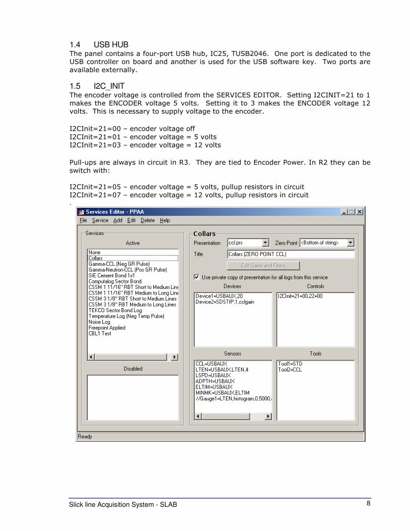
1.5 I2C_INIT The encoder voltage is controlled from the SERVICES EDITOR. Setting I2CINIT=21 to 1
makes the ENCODER voltage 5 volts. Setting it to 3 makes the ENCODER voltage 12
volts. This is necessary to supply voltage to the encoder.
I2CInit=21=00 – encoder voltage off
I2CInit=21=01 – encoder voltage = 5 volts
I2CInit=21=03 – encoder voltage = 12 volts
Pull-ups are always in circuit in R3. They are tied to Encoder Power. In R2 they can be
switch with:
I2CInit=21=05 – encoder voltage = 5 volts, pullup resistors in circuit
I2CInit=21=07 – encoder voltage = 12 volts, pullup resistors in circuit .
9 Slick Line Acquisition System - SLAB
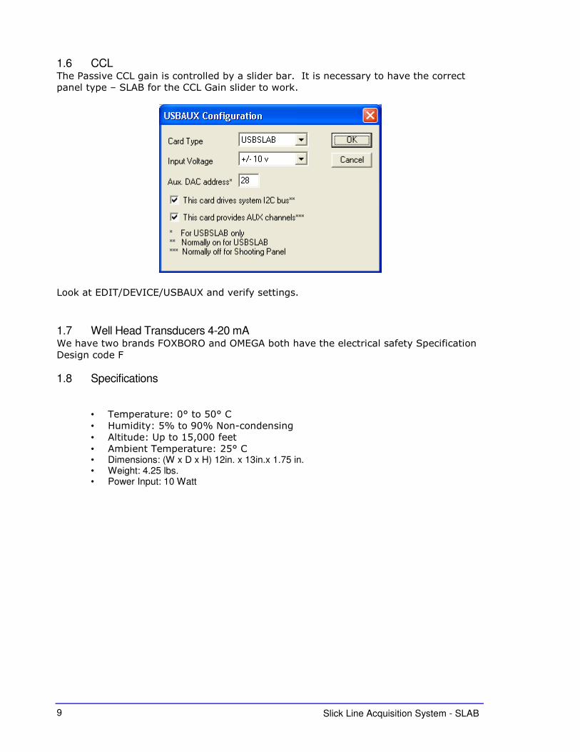
1.6 CCL The Passive CCL gain is controlled by a slider bar. It is necessary to have the correct
panel type – SLAB for the CCL Gain slider to work.
Look at EDIT/DEVICE/USBAUX and verify settings.
1.7 Well Head Transducers 4-20 mA We have two brands FOXBORO and OMEGA both have the electrical safety Specification
Design code F
1.8 Specifications
• Temperature: 0° to 50° C
• Humidity: 5% to 90% Non-condensing
• Altitude: Up to 15,000 feet
• Ambient Temperature: 25° C • Dimensions: (W x D x H) 12in. x 13in.x 1.75 in. • Weight: 4.25 lbs. • Power Input: 10 Watt
10 Slick line Acquisition System - SLAB
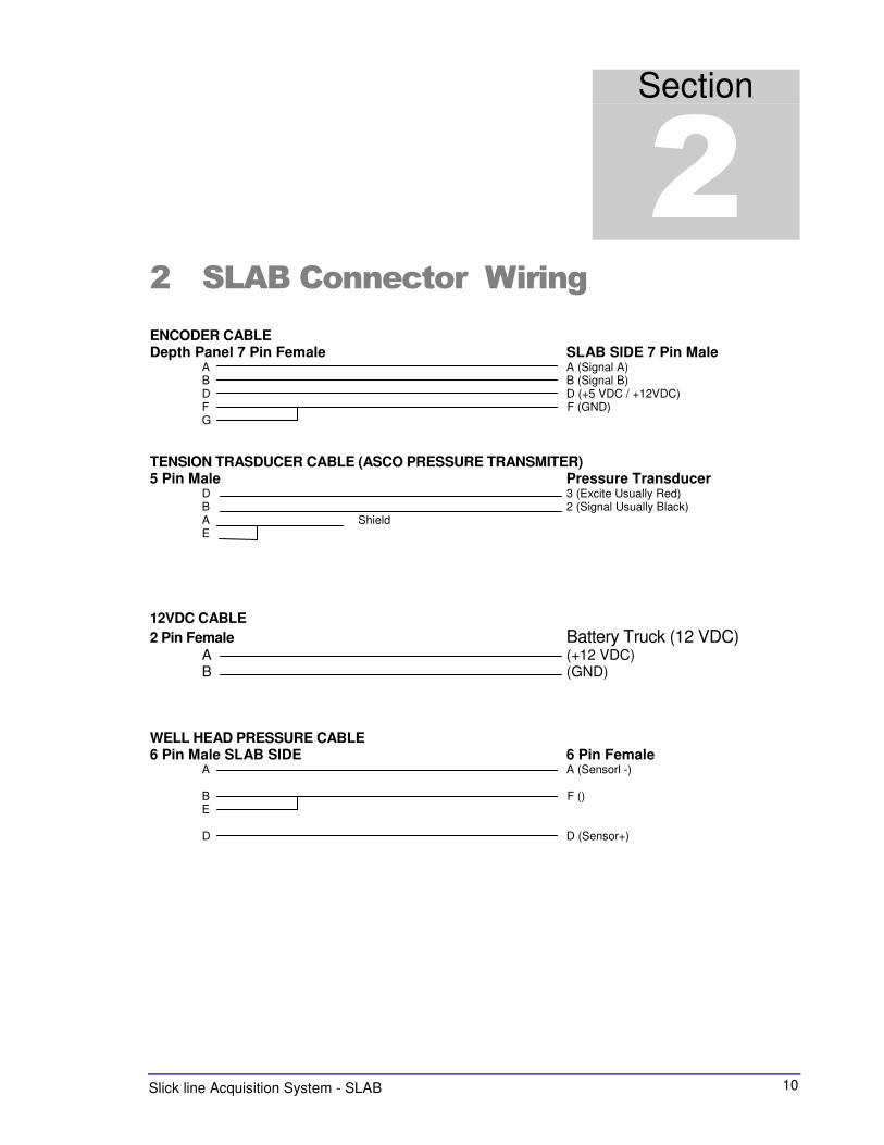
2 SLAB Connector Wiring ENCODER CABLE Depth Panel 7 Pin Female SLAB SIDE 7 Pin Male A A (Signal A) B B (Signal B) D D (+5 VDC / +12VDC) F F (GND) G
TENSION TRASDUCER CABLE (ASCO PRESSURE TRANSMITER) 5 Pin Male Pressure Transducer D 3 (Excite Usually Red) B 2 (Signal Usually Black) A Shield E
12VDC CABLE
2 Pin Female Battery Truck (12 VDC) A (+12 VDC) B (GND) WELL HEAD PRESSURE CABLE 6 Pin Male SLAB SIDE 6 Pin Female A A (Sensorl -) B F () E D D (Sensor+)
Section
2

11 Slick Line Acquisition System - SLAB
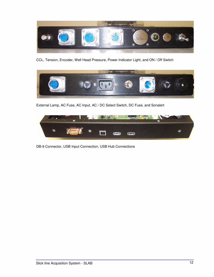
FIG: 2.1 SLAB Panel Connections
12 Slick line Acquisition System - SLAB
CCL, Tension, Encoder, Well Head Pressure, Power Indicator Light, and ON / Off Switch
External Lamp, AC Fuse, AC Input, AC / DC Select Switch, DC Fuse, and Sonalert
DB-9 Connector, USB Input Connection, USB Hub Connections

13 Slick Line Acquisition System - SLAB
FIG: 2.2 SLAB STD Wiring Connections
14 Slick line Acquisition System - SLAB
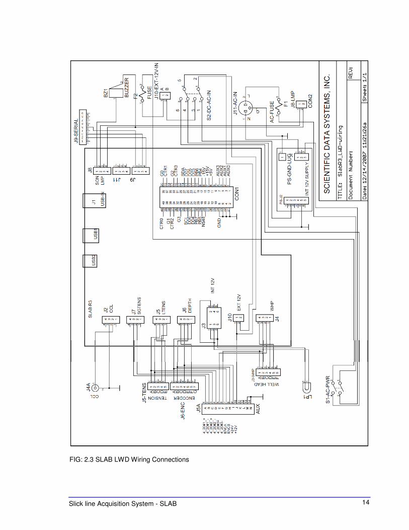
FIG: 2.3 SLAB LWD Wiring Connections

15 Slick Line Acquisition System - SLAB
16 Slick line Acquisition System - SLAB
3 SLAB Main Board Description
Main Board Circuit Description.
SLABR3 sheet 1 of 5
The Cypress AN2131”IC1” is part of the EZ-USB series microcontrollers. It
contains a 8051 core that has 4 clocks per instruction cycle, an auto-incrementing data
pointer with provides FIFO like accesses to its 64 bit onboard RAM . The 8051 includes the
“movx” command for fast two way accesses to the USB port. The microcontroller also has a
built in I2C compatible port.
IC5 is a 128bit EEPROM which holds the initial startup program for the
microcontroller. It communicates over the I2C buss at start up to load the firmware into the
microcontroller.
IC15 is an I2C repeater buffer used to interface between the other I2C peripherals on
the buss and the microcontroller. It is a bi directional interface between the 3.3V components
and the 5V TTL/CMOS components.
IC 7 is a I2C to 8 bit bi directional buss interface. It handles all 8 bit buss to I2C
communications.
IC3 is a tri-state 8 bit buffer tied to IC7’s buss used to latch outputs.
IC2 is a 8 bit A-D with an I2C interface which has direct access to the
microcontroller over the I2C buss. It has an 8 channel multiplexer integrated into the device.
It handles all the A-D channels present on the SLAB board.
IC13 is a 1 MHz crystal whose output is fed into one of 6 counters and used as a
timing signal by the software.
U1 and U2 each have a 3 channel counter which is used to count depth pulses,
1MHz clock and four other input pulses. These counter outputs are directly connected to the
microcontroller over its 8 bit data buss.
IC6 is a DC-DC power supply producing the 3.3V power used by the
microcontroller, EEPROM and I2C repeater ICs.
Section
3
17 Slick Line Acquisition System - SLAB
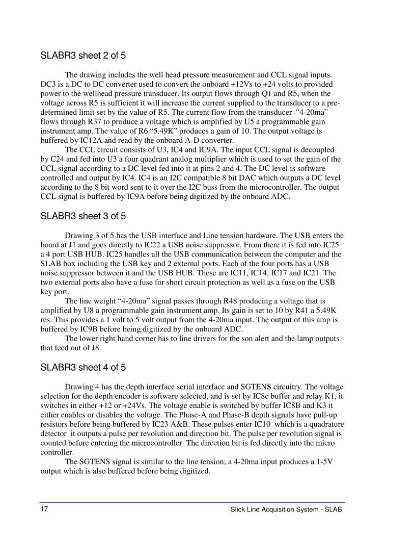
SLABR3 sheet 2 of 5
The drawing includes the well head pressure measurement and CCL signal inputs.
DC3 is a DC to DC converter used to convert the onboard +12Vs to +24 volts to provided
power to the wellhead pressure transducer. Its output flows through Q1 and R5, when the
voltage across R5 is sufficient it will increase the current supplied to the transducer to a pre-
determined limit set by the value of R5. The current flow from the transducer “4-20ma”
flows through R37 to produce a voltage which is amplified by U5 a programmable gain
instrument amp. The value of R6 “5.49K” produces a gain of 10. The output voltage is
buffered by IC12A and read by the onboard A-D converter.
The CCL circuit consists of U3, IC4 and IC9A. The input CCL signal is decoupled
by C24 and fed into U3 a four quadrant analog multiplier which is used to set the gain of the
CCL signal according to a DC level fed into it at pins 2 and 4. The DC level is software
controlled and output by IC4. IC4 is an I2C compatible 8 bit DAC which outputs a DC level
according to the 8 bit word sent to it over the I2C buss from the microcontroller. The output
CCL signal is buffered by IC9A before being digitized by the onboard ADC.
SLABR3 sheet 3 of 5
Drawing 3 of 5 has the USB interface and Line tension hardware. The USB enters the
board at J1 and goes directly to IC22 a USB noise suppressor. From there it is fed into IC25
a 4 port USB HUB. IC25 handles all the USB communication between the computer and the
SLAB box including the USB key and 2 external ports. Each of the four ports has a USB
noise suppressor between it and the USB HUB. These are IC11, IC14, IC17 and IC21. The
two external ports also have a fuse for short circuit protection as well as a fuse on the USB
key port.
The line weight “4-20ma” signal passes through R48 producing a voltage that is
amplified by U8 a programmable gain instrument amp. Its gain is set to 10 by R41 a 5.49K
res. This provides a 1 volt to 5 volt output from the 4-20ma input. The output of this amp is
buffered by IC9B before being digitized by the onboard ADC.
The lower right hand corner has to line drivers for the son alert and the lamp outputs
that feed out of J8.
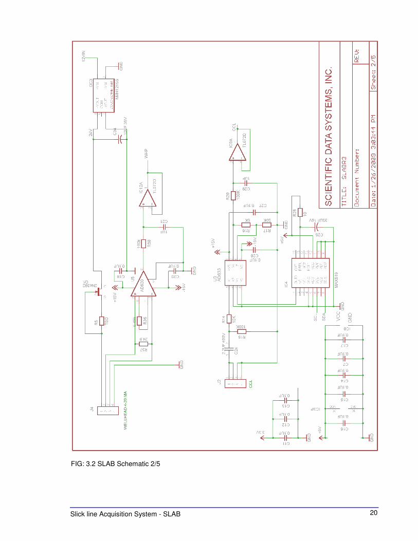
SLABR3 sheet 4 of 5
Drawing 4 has the depth interface serial interface and SGTENS circuitry. The voltage
selection for the depth encoder is software selected, and is set by IC8c buffer and relay K1, it
switches in either +12 or +24Vs. The voltage enable is switched by buffer IC8B and K3 it
either enables or disables the voltage. The Phase-A and Phase-B depth signals have pull-up
resistors before being buffered by IC23 A&B. These pulses enter IC10 which is a quadrature
detector it outputs a pulse per revolution and direction bit. The pulse per revolution signal is
counted before entering the microcontroller. The direction bit is fed directly into the micro
controller.
The SGTENS signal is similar to the line tension; a 4-20ma input produces a 1-5V
output which is also buffered before being digitized.

18 Slick line Acquisition System - SLAB
There is also a serial interface IC20 on the drawing. It interfaces serial TX and RX
data from a single voltage supply to bi-polar RS232 data.
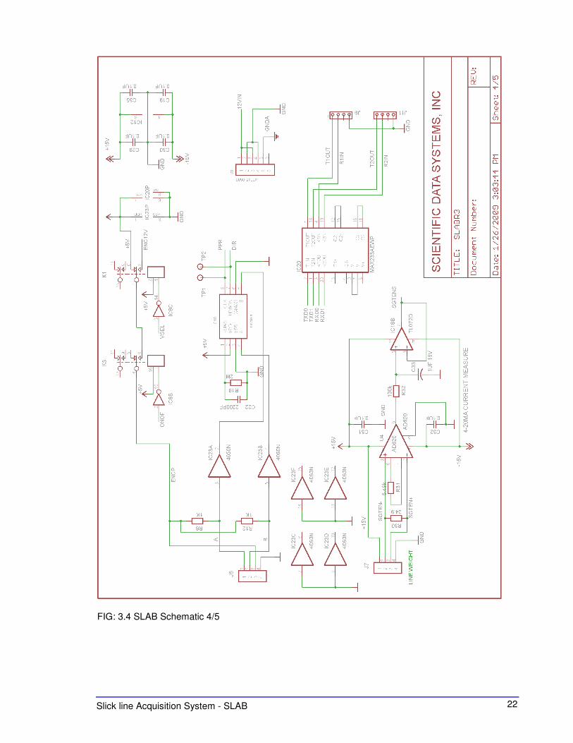
SLABR3 sheet 5 of 5
Sheet 5 has three DC-DC converters. PW2 is a 12V to 12V converter. PW1 is a 12V
to 5V converter and DC2 is a 12V to +-15V converter.

19 Slick Line Acquisition System - SLAB
FIG: 3.1 SLAB Schematic 1/5
20 Slick line Acquisition System - SLAB
FIG: 3.2 SLAB Schematic 2/5

21 Slick Line Acquisition System - SLAB
FIG: 3.3 SLAB Schematic 3/5
22 Slick line Acquisition System - SLAB
FIG: 3.4 SLAB Schematic 4/5
23 Slick Line Acquisition System - SLAB
FIG: 3.5 SLAB Schematic 5/5
24 Slick line Acquisition System - SLAB
FIG: 3.6 SLAB Board

25 Slick Line Acquisition System - SLAB

26 Slick line Acquisition System - SLAB
4 SLAB Wire List
Wire List for SLAB STD & LWD Slick Line Acquisition Box
Feb-12
Connector Outputs
Standard SLAB Specific Wiring
LWD SLAB Specific Wiring
Lamp Out CIR-4F
J8-1 PCB-J8-2 Lamp Out
J8-2 PCB-J8-4 Lamp Return
Buzzer
BZ1-1 PCB-J8-1 Buzzer Out
BZ1-2 PCB-J8-4 Buzzer Return
S1 AC PWR
S1-1 F1-2
S1-2 PS-J1-3
S1-3 F2-2
S1-4 S2-6
Section
4
27 Slick Line Acquisition System - SLAB
S2 AC/DC Switch - DPDT
S2-1 PS-J2-2 Internal 12V Supply +
S2-2 PCB-J10-1
S2-3 J10-B Ext 12v
S2-4 PS-J2-5 Internal 12V Supply -
S2-5 PCB-J10-2
S2-6 S1-4
F1 AC Fuse
F1-1 J11-2 Line In
F1-2 S1-1 AC power switch
F2 DC Fuse .5Amp
F2-1 J10-1 J10 ext
F2-2 S1-3
AC IN
J11-3 PS-GND-Lug AC GND
J11-1 PS-J1-1 AC Neutral
J11-2 F1-1 AC Line In
F1-2 S1-1
S1-2 PS-J1-3 AC Power
MTL Isolator
MTL-1 PCB-J4-1
MTL-2 PCB-J4-2
MTL-3 J3-D
MTL-4 J3-B
LAMP 12-Red
LP1-1 + PCB-J3-2 INT 12v
LP1-2 - PCB-J3-3 INT 12V
J3 Well Head Pressure
J3-A PCB-J4-3 PCB-J4-3 J5A-F
J3-B MTL-4 PCB-J4-2 J5A-E
J3-D MTL-3 PCB-J4-1
J3-E PCB-J4-4 PCB-J4-4
28 Slick line Acquisition System - SLAB
4 CCL-BNC
BNC PCB-J2-2 CCL Signal
BNC GND PCB-J2-3 CCL GND
J5A AUX Outputs LWD
J5A-A PCB-J7-3 SGTENS 4-20ma +
J5A-B PCB-J7-2 SGTENS 4-20ma -
J5A-C J5-B PCB-J5-2 Tension 4-20ma +
J5A-D J5-A PCB-J5-3 Tension 4-20ma-
J5A-E J3-B PCB-J4-2 Well Head 4-20ma+
J5A-F J3-A PCB-J4-3 Well Head 4-20ma-
J5A-G J6-A PCB-J6-1 Encoder Phase A
J5A-H J6-B PCB-J6-2 Encoder Phase A
J5A-I J6-D PCB-J6-3 +24V / +12V Encoder V SEL
J5A-M GND Chassis
J5A-N GND Chassis
J5 Tension - CIR - 5 - F
J5-A PCB-J5-3 J5A-D J5A-D 4-20ma -
J5-B PCB-J5-2 J5A-C J5A-C 4-21ma +
J5-D PCB-J5-1 PCB-J5-1
J5-E PCB-J5-4 PCB-J5-4
J6 Encoder - CIR - 7 - F
J6-A PCB-J6-1 PCB-J6-1 J5A-G Encoder Phase A
J6-B PCB-J6-2 PCB-J6-2 J5A-H Encoder Phase B
J6-D PCB-J6-3 PCB-J6-3 J5A-I +24V / +12V software SEL
J6-F PCB-J6-4 PCB-J6-4
J9 Serial D-9 Male
J9-2 PCB-J9-4
J9-3 PCB-J9-3
J9-5 PCB-J9-1
J10 EXT 12V In
J10-1 F2-2 External 12V
J10-2 S2-3

29 Slick Line Acquisition System - SLAB
PCB Board Connectors
PCB J1 USB In
J1 USB - USB IN USB Hub In
PCB J2 CCL In
J2-1 NC
J2-2 J4-1 CCL Input
J2-3 J4-2 GND
J2-4 NC
PCB J3 INT 12V
J3-1 J3-3 LP1-2 Lamp 12V
J3-2 J3-4 LP1-1 Lamp 12V
J3-3 J3-1 LP1-2 Lamp 12V
J3-4 J3-2 LP1-1 Lamp 12V
J3-5 NC
J3-6 NC
PCB J4 Well head Pressure
J4-1 MTL-1 J3-D
J4-2 MTL-2 J3-B J5A-E Well Head Press 4-20ma +
J4-3 J3-A J3-A J5A-F Well Head Press 4-20ma-
J4-4 J3-E J3-E
PCB J5 Surface tension
J5-1 J5-D J5-D
J5-2 J5-B J5-B J5A-C Surface tension 4-20ma +
J5-3 J5-A J5-A J5A-D Surface tension 4-20ma -
J5-4 J5-E J5-E
PCB J6 Depth
J6-1 J6-A J6-A J5A-G Phase A
J6-2 J6-B J6-B J5A-H Phase B
J6-3 J6-D J6-D J5A-I +24 / +12V Encoder Power
J6-4 J6-F J6-F GND
30 Slick line Acquisition System - SLAB
PCB J7 SGTENS
J7-1 NC
J7-2 J5A-B SGTENS 4-20ma -
J7-3 J5A-A SGTENS 4-20ma +
J7-4 NC
PCB J8 SON Buzzer & Lamp
J8-1 BUZ-1 Buzzer signal
J8-2 J8-LMP-1 Lamp signal
J8-3 NC
J8-4 BUZ-2 J8-LMP-2 Buzzer & Lamp GND
PCB J9 Serial 9 Pin D
J9-1 J9-5 Return
J9-2 NC
J9-3 J9-3 RS232
J9-4 J9-2 RS232
PCB J10 Ext 12V
J10-1 S2-2
J10-2 S2-5
PCB J11 NC
J11-1 NC
J11-2 NC
J11-3 NC
J11-4 NC