single phase transformerless semi-z … phase transformerless semi-z-source inverter with ... to the...
TRANSCRIPT

SINGLE PHASE TRANSFORMERLESS SEMI-Z-SOURCE INVERTER WITH REDUCED TOTAL
HARMONIC DISTORTION (THD) AND DC CURRENT INJECTION
Tofael Ahmed, Saad Mekhilef Department of Electrical Engineering
Faculty of Engineering, University of Malaya Kuala Lumpur, Malaysia
[email protected], [email protected]
Abstract- A single phase transformerless semi-Z-source
inverter topology is presented in this paper in order to
incorporate distributed photovoltaic generators to the grid with
reduced total harmonic distortion (THD) and DC current
injection. These proposed inverter topologies are capable of
achieving the sinusoidal output voltage by using only two active
switches whereas the traditional inverters require four. A
modified form of nonlinear SPWM technique is employed here to
overcome the nonlinear voltage gain problem of semi-Z-source
inverter for providing desired duty cycle which generates the
sinusoidal voltage at the output. This inverter topology shows less
DC current injection to the grid. Furthermore, common ground
is being shared by both DC input and AC output voltage; hence
common mode leakage current gets mitigated. Finally, a
prototype rated SOW is constructed and a verification of
theoretical outcome with the results of the experimental setup are
presented. The results of the experiments satisfy the effectiveness
of the aforementioned topology.
Keywords-Transformerless Inverter,
inverter, Common mode leakage current,
Generators.
I. INTRODUCTION
Semi-Z-source
Distributed
Power supplied to the utility grid from renewable energy distributed generators (DGs), like wind turbine, solar photo voltaic (PV), and fuel cell are becoming more and more visible now-a-days. This is because of the increasing clean energy demand, rapid development of rural area and the concern regarding environmental pollution around the world. These renewable energy DGs only capable of producing DC voltage at the output, while, to connect these DGs with grid, it requires AC voltage. To interconnect utility grid and DGs, inverters should be placed between DGs and grid to realize power conversion and control optimization [1, 2].
Several inverter topologies have been discussed in [3-8]. Inverters can be divided in two types on the basis on galvanic isolation namely, isolated and non-isolated inverters [9-13]. The problem of using these isolated inverters not only increases the system cost and size but also reduce overall efficiency because it contains high frequency or line frequency transformer for electrical isolation [12, 14-16]. In contrast to that non-isolated inverter concept, lessen cost and reduce size along with improved efficiency. Presently, in the low voltage grid, galvanic isolation is not required. So, transformerless inverters have turned into the market mainstream [8, 17].
Mutsuo N akaoka Kyungnam University
Masan, Kyungnam, South Korea [email protected]
Unfortunately transformerless systems require some safety issues to be included. It needs to minimize connection effect between the input DC source and the grid, especially if PV cell exists. If same ground is not shared by the PV cell and the grid a variable common mode is developed. As a result, large common mode leakage current may flows through the parasitic capacitor between PV array and the ground [8, 18-20].
Conventionally, half or full bridge inverters were used to mitigate the problem of common mode leakage current using bipolar SPWM. As a result, no variable common mode voltage is generated. But, it requires approximately greater than 700V of DC voltage to produce 220Vac at the output. As a consequence, series connection of large numbers of PV array or high conversion ratio dc/dc converter is required. On the other hand, the full bridge inverter topology requires 50% of the input voltage than that of half bridge topology (approximately greater than 350V for 220Vac) [20]. But, the disadvantages of full bridge inverter topology are, high current ripple, lower efficiency and large filter inductor. Another solution to solve the common mode leakage current problem is to use doubly grounded topologies because, these topologies contain simple circuit design, lower investments cost and ensure safety [8, 18, 21]. So, preference is given to doubly grounded transformerless topologies.
Some operational issues those should be taken into consideration for transformerless grid connected systems are, total harmonic distortion (THD), output current regulation, and DC current injection. The IEEE and the IEC standards give some bindings on the maximum range of THD and injected DC current [22, 23]. Acute attention is needed for the DC current injection because this may flows through distribution transformer, energy meters and residual current devices [24, 25]. DC current cause saturation to distribution transformer and decrease the efficiency and error the measurement of energy meter. The ranges of this DC current injection are different around the world. This limit varies from 5 rnA in the UK to I
A in Germany [26, 27] and 0.5% -1% of the rated output current of the inverter [22, 23].
To improve the system reliability and minimize cost, some transformerless inverter topology based on Z-source and quasiZ-source have been presented for PV application in [13, 28-33]. Recently, in [34], semi Z source inverter for single phase PV system has been proposed. Doubly grounded features are not included in most of these topologies. Only [34] shows the
978-1-4799-0482-2/13/$31.00 ©2013 IEEE 1322
ground sharing option between grid and inverters. But [34] does not provide the THD and DC current injection analysis.
A single stage transforrnerless semi-Z-source inverter for grid connected application for renewable energy DGs is presented in this paper. This inverter minimizes common mode leakage current with its ground sharing features, ensures less THD and DC current injections to the grid. This topology has some benefits over traditional Z source inverter topology. It contains Z source network in AC side of the semi-Z-source network which is different from conventional topology and results in size minimization. To generate sinusoidal voltage at the output, the proposed topology uses the nonlinear sinusoidal voltage gain curve as voltage reference.
Section I contains an introduction specifying the rational of the project described in this paper. Basic principles of the transformerless semi-z-source inverters are briefly described in section II followed by the modulation principles in section III. Section IV provides required equations for design. Section V describes the important detail of experimental setup as well as the results obtained and their discussion. At last, section VI includes the conclusion drawn from all the above discussed section.
II. BASIC PRINCIPLE OF TRANSFORMERLESS SEMI-Z-SOURCE
INVERTER
Z-source and quasi-Z-source dc-dc converters are shown in Fig. 1 which have the ground sharing nature [13]. Fig. 2 shows the continuous voltage gain curve of Fig. l. Topologies shown in Fig. I have the ability to produce positive and negative voltage at the output with continuous voltage gain curve. So, within duty cycle from 0 to 2/3 and appropriate modulation strategy, these two topologies can be used as inverter with -Yin to +Yin at the output as like as the traditional full bridge inverter.
(a) (b)
Fig. l. Z-source and quasi-Z-source dc-dc converters with continuous voltage gain.
o
.� -1 Q a -2 .s -0 > ·3
·4
Fig. 2. Voltage gain curve.
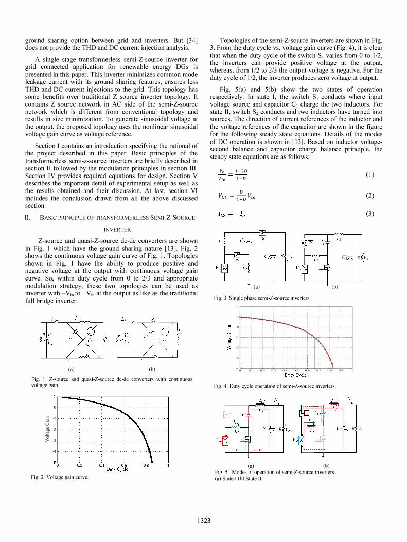
Topologies of the semi-Z-source inverters are shown in Fig. 3. From the duty cycle vs. voltage gain curve (Fig. 4), it is clear that when the duty cycle of the switch Sj varies from 0 to 1/2, the inverters can provide positive voltage at the output, whereas, from 1/2 to 2/3 the output voltage is negative. For the duty cycle of 1/2, the inverter produces zero voltage at output.
Fig. 5(a) and 5(b) show the two states of operation respectively. In state I, the switch Sl conducts where input voltage source and capacitor Cj charge the two inductors. For state II, switch S2 conducts and two inductors have turned into sources. The direction of current references of the inductor and the voltage references of the capacitor are shown in the figure for the following steady state equations. Details of the modes of DC operation is shown in [13]. Based on inductor voltagesecond balance and capacitor charge balance principle, the steady state equations are as follows;
Vo 1-2D
Vin I-D
D VCl = - V;n I-D
(a)
Fig. 3. Single phase semi-Z-source inverters.
·3
L,
C,
(b)
�O��R�' �Q�2�=�� o . • ��n'��O.�6�R� 7 ���ft�9 � Duty Cycle
Fig. 4. Duty cycle operation of semi-Z-source inverters.
(1)
(2)
(3)
+
R Vo
+
R Vo
(a) (b) Fig. 5. Modes of operation of semi-Z-source inverters. (a) State I (b) State II
l323
D ILl = - - 10 1-D (4)
[f we assume that, (5) is the output voltage of the inverter then the modulation index can be expressed as in (6). Equation (7) has been derived from (1), (5), and (6). 0' = [-0, the duty cycle of the switch S2 which can be expressed as (8).
Va = V sinwt
D = 1-Msinwt 2-Msinwt
D' = __ 1
__ 2-Msinwt
(5)
(6)
(7)
(8)
III. SEMI-Z-SOURCE INVERTERS MODULATION PRINCIPLE
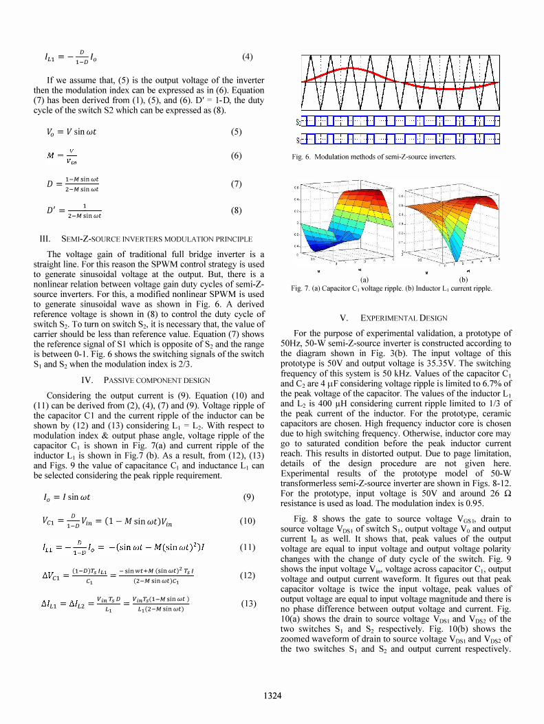
The voltage gain of traditional full bridge inverter is a straight line. For this reason the SPWM control strategy is used to generate sinusoidal voltage at the output. But, there is a nonlinear relation between voltage gain duty cycles of semi-Zsource inverters. For this, a modified nonlinear SPWM is used to generate sinusoidal wave as shown in Fig. 6. A derived reference voltage is shown in (8) to control the duty cycle of switch S2. To turn on switch S2, it is necessary that, the value of carrier should be less than reference value. Equation (7) shows the reference signal of S I which is opposite of S2 and the range is between 0-1. Fig. 6 shows the switching signals of the switch Sl and S2 when the modulation index is 2/3.
IV. PASSIVE COMPONENT DESIGN
Considering the output current is (9). Equation (10) and (11) can be derived from (2), (4), (7) and (9). Voltage ripple of the capacitor C I and the current ripple of the inductor can be shown by (12) and (13) considering Ll = L2. With respect to modulation index & output phase angle, voltage ripple of the capacitor C1 is shown in Fig. 7(a) and current ripple of the inductor Ll is shown in Fig.7 (b). As a result, from (12), (13) and Figs. 9 the value of capacitance C1 and inductance Ll can be selected considering the peak ripple requirement.
10 = I sin wt
VCl = � Vin = (1 - M sin wt)Vin 1-D
A V: _
(l-D)TsILl _
-sinwt+M (sinwt)2 TsI Ll C1 - -C1 (2-M sin wt)C1
AI _ AI _ Vin TsD
_ VinTs(l-Msinwt )
Ll L1 - Ll L2 - -L1 L1(2-M sin wt)
(9)
(10)
( I I )
(12)
(13)
slOJl]··i··U·· ; ·U}LJR][LJJLJ{O}Ul sfOJl]··:··U··;·O}OJOJfJU····ClJlLJJ
Fig. 6. Modulation methods of semi-Z-source inverters.
(a) (b) Fig. 7. (a) Capacitor C1 voltage ripple. (b) Inductor Ll current ripple.
V. EXPERIMENTAL DESIGN
For the purpose of experimental validation, a prototype of 50Hz, 50-W semi-Z-source inverter is constructed according to the diagram shown in Fig. 3(b). The input voltage of this prototype is 50V and output voltage is 35.35V. The switching frequency of this system is 50 kHz. Values of the capacitor C1 and Cz are 4 /IF considering voltage ripple is limited to 6.7% of the peak voltage of the capacitor. The values of the inductor Ll and Lz is 400 /lH considering current ripple limited to 1/3 of the peak current of the inductor. For the prototype, ceramic capacitors are chosen. High frequency inductor core is chosen due to high switching frequency. Otherwise, inductor core may go to saturated condition before the peak inductor current reach. This results in distorted output. Due to page limitation, details of the design procedure are not given here. Experimental results of the prototype model of 50-W transformerless semi-Z-source inverter are shown in Figs. 8-12. For the prototype, input voltage is 50V and around 26 (2 resistance is used as load. The modulation index is 0.95.
Fig. 8 shows the gate to source voltage V GSl, drain to source voltage VDS1 of switch S), output voltage Vo and output current 10 as well. It shows that, peak values of the output voltage are equal to input voltage and output voltage polarity changes with the change of duty cycle of the switch. Fig. 9 shows the input voltage V in, voltage across capacitor C), output voltage and output current waveform. It figures out that peak capacitor voltage is twice the input voltage, peak values of output voltage are equal to input voltage magnitude and there is no phase difference between output voltage and current. Fig. 10(a) shows the drain to source voltage VDS1 and VDSZ of the two switches Sl and Sz respectively. Fig. I O(b) shows the zoomed waveform of drain to source voltage V DS 1 and V DS2 of the two switches Sl and Sz and output current respectively.
l324

10
o S.OOMS/S 0 f 210e 2012 1M olnl5 O.OOV 12:32:31
o IOOY .. IOOY 20.0ms S,OOMS/S U J 21 Dec 2012 200 A ij-o"'-S.06'58Dms 1M Int$ 0,00 V I G:ll :55
Fig. 8. Gate to source voltage, drain to source voltage, output voltage, Fig. 9. Input voltage, capacitor C] voltage, output voltage, Output output current. current.
un u 0
U IOOV 100 V IQ.Oms ID.OMS/S ij-. ..... O.OOOOO 5 1M Ints
(a)
4.00)Js 2.50GS/s 0 ....... 5 ... '"'000"$ 1M InU
(b)
J 21 Dec 2012 0.00 V 13:01: 12
Fig. 10. (a) Drain to source voltage of two switches. (b) Zoomed in waveform of drain to source voltage of two switches and output current.
- I.., ,ott. . .., ."" J-� .. itt'f
Urms1 35.52 V Irms1 1.368 A Uthd1 4.385 % Ithd1 4.377 %
�. ..6 •
....... : 1 0 ••• : ..
Fig. 11. THO of output voltage, output current.
From this Fig. it can be seen that two switches are operating in complementary manner. Fig.11 shows the THD of the output voltage and output current waveforms. Figs. 12(a), (b) show the harmonic spectrum of output voltage and current and these two Figs. show that THD's are within the limit (less than 5%) and alike no occurrence of DC current (limits are 0.5% - I % of the rated current) at the output and the values of the output voltage and currents are 35.45V and 1.36A respectively.
Semi-Z-source inverter utilizes only two switches rather than four switches as of traditional single-phase inverter or Z source inverters, which minimizes the cost. For grid connected application, the designed semi-Z-source inverter injects less
1325
r U lit
� O.OV
lar 1.
r I 1 • o.� Ii
I)
(a)
(b)
VI+ l5.45V VI x dY1 Order+: I OrderX: �o
\'1 + 1.363 A YIX AY1 Order +: I Orderx: �O
Fig. 12. (a) THO of output voltage, (b) THO of output current.

voltage harmonic (less than 5%) and no DC current component to the grid which satisfies the IEEE and IEC standards as stated in [22, 23]. Moreover, this transformerless topology has less effect of the higher order harmonics. The semi-Z-source network utilizes the Z source network in AC side rather than DC side compared with the traditional Z source network. For this reason, the total size of transformerless semi-Z-source inverter is not large like the traditional Z source network.
VI. CONCLUSION
This paper presents a transformerless inverter system to interface renewable energy DGs to grid after reviewing latest topology. By using two switches and a modified nonlinear SPWM, this topology can generate sinusoidal voltage at the output. As the input and output terminals share the same ground that minimizes the leakage current between grid and DGs. Furthermore, this topology ensures less THD and DC current injection to the grid. The performance of this topology can be improved by choosing efficient inductor design and can be expanded to two-phase or three phase very easily that can utilize the total range of the duty cycle.
ACKNOWLEDGMENT
The authors would like to thank the Ministry of Higher Education of Malaysia and University of Malaya for providing financial support under the research grant No.UM.C/HIRlMOHEIENG/16001-00-DOOOOI7.
REFERENCES
[1] F. Blaabjerg, R. Teodorescu, M. Liserre, and A. V. Timbus, "Overview of control and grid synchronization for distributed
power generation systems," IEEE Transactions on Industrial
Electronics, vol. 53, pp. 1398-1409, Oct 2006. [2] H. M. Kojabadi, B. Yu, I. A. Gadoura, L. C. Chang, and M. Ghribi,
"A novel DSP-based current-controlled PWM strategy for single phase grid connected inverters," IEEE Transactions on Power Electronics, vol. 21, pp. 985-993, Jul 2006.
[3] M. K. Menshawi and S. Mekhilef, "Multistage Inverters Control Using Surface Hysteresis Comparators," JOURNAL OF POWER
ELECTRONICS, vol. 13, pp. 59-69,2013. [4] S. Mekhilef and M. A. Kadir, "Novel vector control method for
three-stage hybrid cascaded multilevel inverter," IEEE
Transactions on Industrial ElectroniCS, vol. 58, pp. 1339-1349, 2011.
[5] S. Mekhilef, "Dual vector control strategy for a three-stage hybrid cascaded multilevel inverter," Journal of Power Electronics, vol. 10, pp. 155-164,2010.
[6] M. K. S. Mekhilef, "HW Ping Voltage Vector Control of a Hybrid Three-Stage Eighteen-Level Inverter by Vector Decomposition," lET Transaction on Power Electronics, vol. 3, pp. 601-611,2010.
[7] S. Mekhilef and A. Kadir, "Voltage control of three-stage hybrid multilevel inverter using vector transformation," IEEE
Transactions on Power Electronics, vol. 25, pp. 2599-2606, 2010. [8] S. V. Araujo, P. Zacharias, and R. Mallwitz, "Highly eflicient
single-phase transforrnerless inverters for grid-connected photovoltaic systems," IEEE Transactions on Industrial Electronics, vol. 57, pp. 3118-3128, 2010.
[9] S. Mekhilef, M. N. A. Kadir, and Z. Salam, "Digital Control of Three Phase Three-Stage Hybrid Multilevel Inverter," IEEE
Transactions on Industrial Informatics, vol. 9, pp. 719-727, May 2013.
[10] S. Mekhilef, N. Rahim, and A. Omar, "A new solar energy conversion scheme implemented using grid-tied single phase inverter," in TENCON 2000. Proceedings, 2000, pp. 524-527.
[II] S. K. Kamali and S. Mekhilef, "Evaluation study on gridconnected PV system at University of Malaya," in International
[12]
[13]
[14]
[15]
[16]
[17]
[18]
[19]
[20]
[21]
[22]
[23]
[24]
[25]
[26]
[27]
[28]
[29]
[30]
1326
Conference for Technical Postgraduates (TECHPOS), 2009 2009, pp. 1-7. T. Kerekes, R. Teodorescu, M. Liserre, C. Klumpner, and M. Sumner, "Evaluation of Three-Phase Transformerless Photovoltaic Inverter Topologies," IEEE Transactions on Power Electronics, vol. 24, pp. 2202-2211, Sep 2009. D. Cao and F. Z. Peng, "A family of Z-source and quasi-Z-source DC-DC converters," in Twenty-Fourth Annual IEEE Applied Power Electronics Conference and Exposition, 2009. APEC 2009, 2009, pp. 1097-1101. M. Abdolrasol and S. Mekhile±: "Hybrid anti-islanding algorithm for utility interconnection of distributed generation," in International Conference for Technical Postgraduates (TECHPOS), 2009, pp. 1-5. S. Mekhilef, R. Saidur, and A. Safari, "A review on solar energy use in industries," Renewable & Sustainable Energy Reviews, vol. 15, pp. 1777-1790, May 2011. N. Rahim and S. Mekhilef, "Implementation of three-phase grid connected inverter for photovoltaic solar power generation system," in International Conference on Power System Technology, 2002. Proceedings. PowerCon 2002, 2002, pp. 570-573. (2001, Eigenerzeugungsanlagen am NiederspannungsnetzRichtlinie fUr AnschluB und Parallelbetrieb von Eigenerzeugungsanlagen am Niederspannungsnetz (Energy Generation Equipment Connected to the Low Voltage GridGuideline for the Connection and Parallel Operation of Energy Generation Equipment on Low Voltage Grid). O. Lopez, F. D. Freijedo, A. G. Yepes, P. Fernandez-Comesana, J. Malvar, R. Teodorescu, et aI., "Eliminating Ground Current in a Transformerless Photovoltaic Application," IEEE Transactions on Energy Conversion, vol. 25, pp. 140-147, Mar 2010. H. F. Xiao and S. J. Xie, "Leakage Current Analytical Model and Application in Single-Phase Transformerless Photovoltaic GridConnected Inverter," IEEE Transactions on Electromagnetic
Compatibility, vol. 52, pp. 902-913, Nov 2010. B. Yang, W. H. Li, Y. J. Gu, W. F. Cui, and X. N. He, "Improved Transformerless Inverter With Common-Mode Leakage Current Elimination for a Photovoltaic Grid-Connected Power System," IEEE Transactions on Power Electronics, vol. 27, pp. 752-762, Feb 2012. F. Zhang, S. Yang, F. Z. Peng, and Z. Qian, "A zigzag cascaded multilevel inverter topology with self voltage balancing," in Twenty-Third Annual IEEE Applied Power Electronics Conference and Exposition, APEC 200B, 2008, pp. 1632-1635. "IEEE Standard for Interconnecting Distributed Resources With
Electric Power Systems," IEEE Std 1547-2003, pp. 0_1-16,2003. "Characteristics of the Utility Interface for Photovoltaic (PV)
Systems," IEC 61727, Ed. 2, 2004. A. R. Martina Calais, and M. Dymond, "Transformerless PV Inverter Issues Revisited, Are Australian Standards Adequate?," in
Solar09, the 47th ANZSES Annual Conference. Townsville, Queensland, Australia, 29 September-2 October 2009. R. B. B. Bletterie, C. Mayr, J. Kirchhof, M. Moschakis, N. Hatziargyriou, and S. Nguefeu, "Identification of general safety problems , definition of test procedures and design-measures for protection," 2006. "Engineering Recommendation, United Kingdom ER G83/1
Recommendations for the Connection of Small-Scale Embedded Generations (up to 16 A per phase) in Parallel With Public LowVoltage Distribution Network," Sep. 2003. "DIN V VDE V 0126-1-1 Automatic Disconnection Device
Between a Generator and the Public Low-Voltage Grid," Berlin,
Germany: VDE Press, 2006, 9 pp. J. Anderson and F. Peng, "A class of quasi-Z-source inverters," in Industry Applications Society Annual Meeting, 200B. IAS'OB. IEEE, 2008, pp. 1-7. Y. Huang, M. S. Shen, F. Z. Peng, and J. Wang, "Z-source inverter for residential photovoltaic systems," IEEE Transactions on Power Electronics, vol. 21, pp. 1776-1782, Nov 2006. F. Z. Peng, "Z-source inverter," IEEE Transactions on Industry Applications, vol. 39, pp. 504-510, Mar-Apr 2003.

[31] S. Rajakaruna, "Experimental studies on a novel single-phase ZSource inverter for grid connection of renewable energy sources," in Power Engineering Conference. 2008. AUPEC'08. Australasian
Universities, 2008, pp. 1-6. [32] M. Shahparasti, A. Sadeghi Larijani, A. Fatemi, A. Yazdian
Va�jani, and M. Mohammadian, "Quasi Z-source inverter for photovoltaic system connected to single phase AC grid," in 1st
Power Electronic & Drive Systems & Technologies Conference (PEDSTC). 2010,2010, pp. 456-460.
[33] D. Vinnikov and 1. Roasto, "Quasi-Z-source-based isolated DC/DC converters for distributed power generation," IEEE Transactions on Industrial Electronics, vol. 58, pp. 192-201,2011.
[34] D. Cao, S. Jiang, X. Yu, and F. Z. Peng, "Low-Cost Semi-Z-source Inverter for Single-Phase Photovoltaic Systems," IEEE Transactions on Power Electronics, vol. 26, pp. 3514-3523,2011.
1327