si838x data sheet - silabs.com · si838x data sheet bipolar digital field inputs for plcs and...
TRANSCRIPT
Si838x Data Sheet
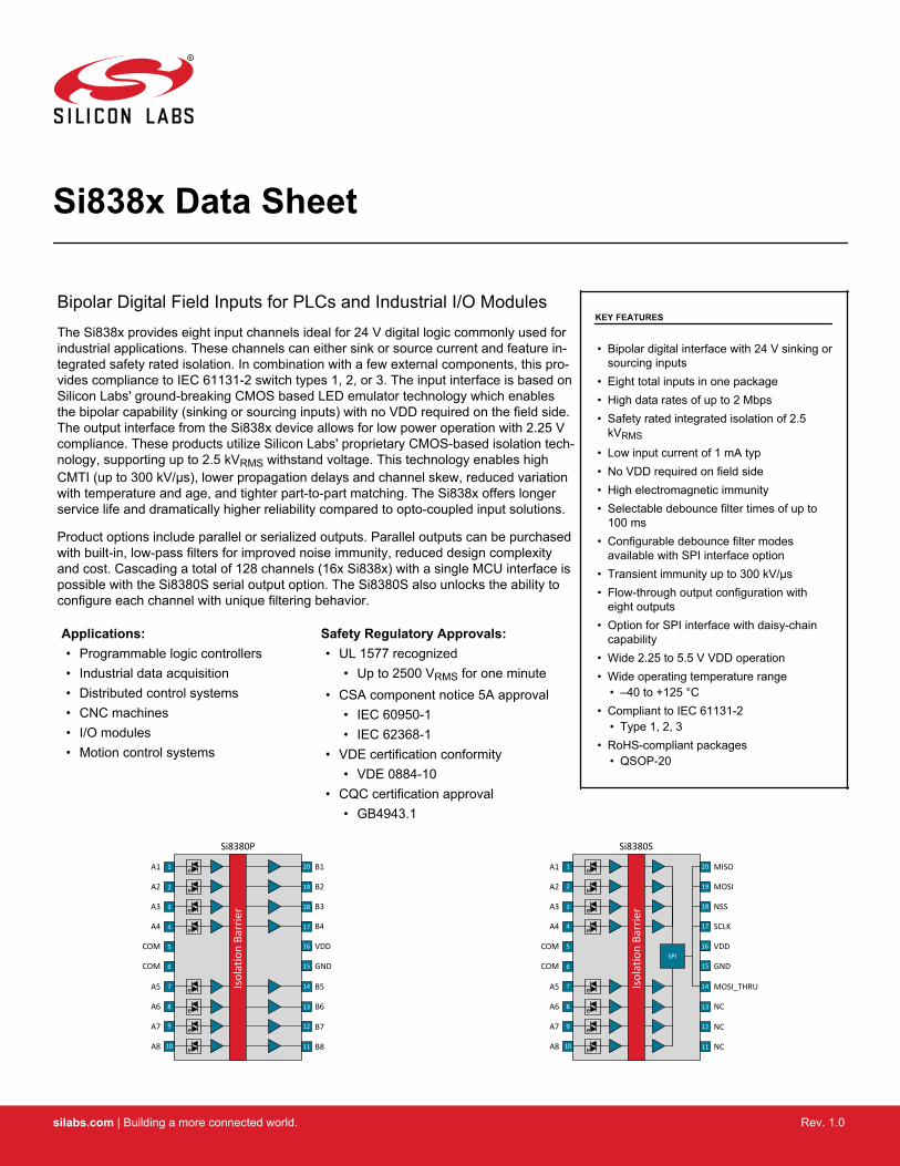
Bipolar Digital Field Inputs for PLCs and Industrial I/O ModulesThe Si838x provides eight input channels ideal for 24 V digital logic commonly used forindustrial applications. These channels can either sink or source current and feature in-tegrated safety rated isolation. In combination with a few external components, this pro-vides compliance to IEC 61131-2 switch types 1, 2, or 3. The input interface is based onSilicon Labs' ground-breaking CMOS based LED emulator technology which enablesthe bipolar capability (sinking or sourcing inputs) with no VDD required on the field side.The output interface from the Si838x device allows for low power operation with 2.25 Vcompliance. These products utilize Silicon Labs' proprietary CMOS-based isolation tech-nology, supporting up to 2.5 kVRMS withstand voltage. This technology enables highCMTI (up to 300 kV/μs), lower propagation delays and channel skew, reduced variationwith temperature and age, and tighter part-to-part matching. The Si838x offers longerservice life and dramatically higher reliability compared to opto-coupled input solutions.
Product options include parallel or serialized outputs. Parallel outputs can be purchasedwith built-in, low-pass filters for improved noise immunity, reduced design complexityand cost. Cascading a total of 128 channels (16x Si838x) with a single MCU interface ispossible with the Si8380S serial output option. The Si8380S also unlocks the ability toconfigure each channel with unique filtering behavior.
Applications:• Programmable logic controllers• Industrial data acquisition• Distributed control systems• CNC machines• I/O modules• Motion control systems
Safety Regulatory Approvals:• UL 1577 recognized
• Up to 2500 VRMS for one minute• CSA component notice 5A approval
• IEC 60950-1• IEC 62368-1
• VDE certification conformity• VDE 0884-10
• CQC certification approval• GB4943.1
KEY FEATURES
• Bipolar digital interface with 24 V sinking orsourcing inputs
• Eight total inputs in one package• High data rates of up to 2 Mbps• Safety rated integrated isolation of 2.5
kVRMS
• Low input current of 1 mA typ• No VDD required on field side• High electromagnetic immunity• Selectable debounce filter times of up to
100 ms• Configurable debounce filter modes
available with SPI interface option• Transient immunity up to 300 kV/μs• Flow-through output configuration with
eight outputs• Option for SPI interface with daisy-chain
capability• Wide 2.25 to 5.5 V VDD operation• Wide operating temperature range
• –40 to +125 °C• Compliant to IEC 61131-2
• Type 1, 2, 3• RoHS-compliant packages
• QSOP-20
A2
A3
A4
A7
A8
A5
A6
1
2
3
4
5
6
9
10
19
18
17
16
15
A1
COM
COM
B1
B2
B3
B4
VDD
GND
B7
B8
7
8
B5
B6
Si8380P
14
12
11
20
13
e
e
e
e
e
e
e
e
Isol
atio
n Ba
rrie
r
1
2
3
4
5
6
9
10
19
18
17
16
15
A1
A2
A3
A4
COM
COM
A7
A8
MISO
MOSI
NSS
SCLK
VDD
GND
NC
NC
7
8
A5
A6
MOSI_THRU
NC
Si8380S
14
12
11
20
13
Isol
atio
n Ba
rrie
r
SPI
e
e
e
e
e
e
e
e
silabs.com | Building a more connected world. Rev. 1.0
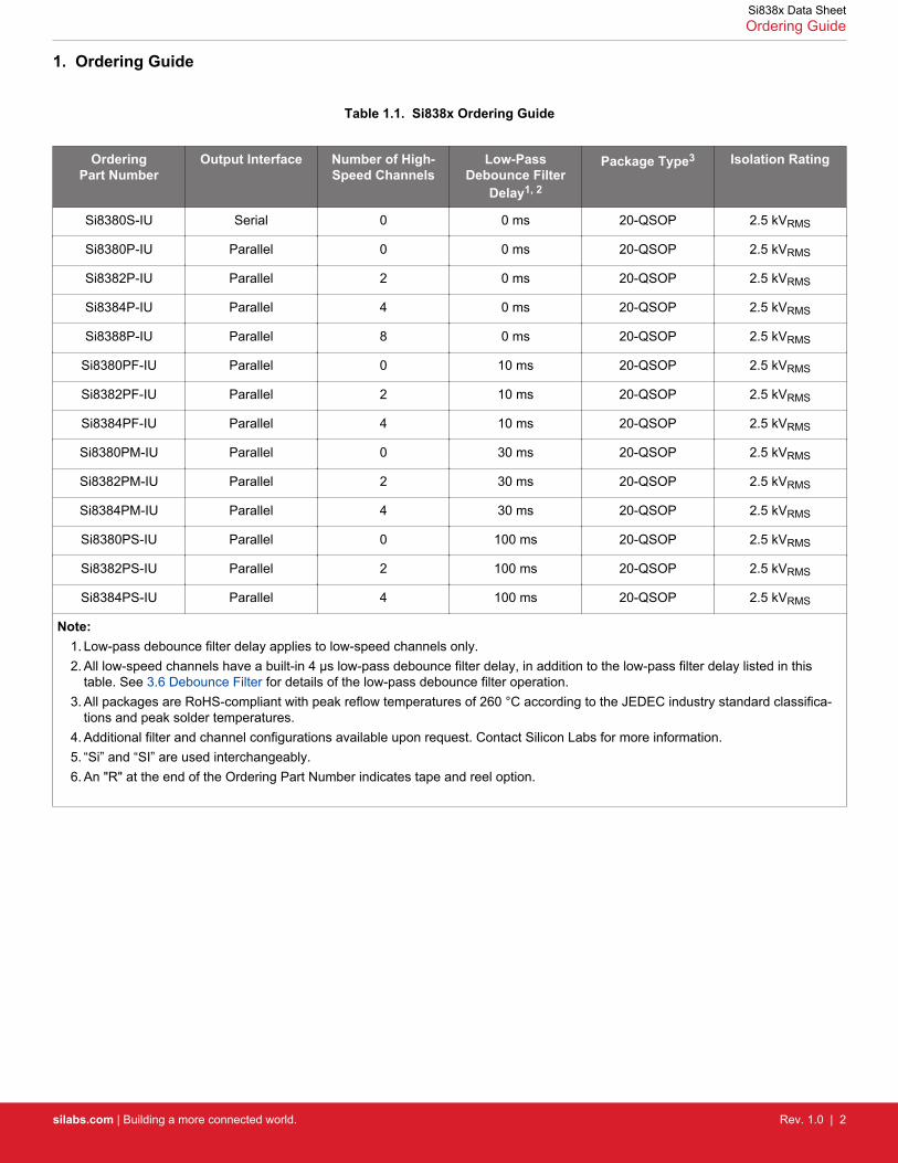
1. Ordering Guide
Table 1.1. Si838x Ordering Guide
OrderingPart Number
Output Interface Number of High-Speed Channels
Low-PassDebounce Filter
Delay1, 2
Package Type3 Isolation Rating
Si8380S-IU Serial 0 0 ms 20-QSOP 2.5 kVRMS
Si8380P-IU Parallel 0 0 ms 20-QSOP 2.5 kVRMS
Si8382P-IU Parallel 2 0 ms 20-QSOP 2.5 kVRMS
Si8384P-IU Parallel 4 0 ms 20-QSOP 2.5 kVRMS
Si8388P-IU Parallel 8 0 ms 20-QSOP 2.5 kVRMS
Si8380PF-IU Parallel 0 10 ms 20-QSOP 2.5 kVRMS
Si8382PF-IU Parallel 2 10 ms 20-QSOP 2.5 kVRMS
Si8384PF-IU Parallel 4 10 ms 20-QSOP 2.5 kVRMS
Si8380PM-IU Parallel 0 30 ms 20-QSOP 2.5 kVRMS
Si8382PM-IU Parallel 2 30 ms 20-QSOP 2.5 kVRMS
Si8384PM-IU Parallel 4 30 ms 20-QSOP 2.5 kVRMS
Si8380PS-IU Parallel 0 100 ms 20-QSOP 2.5 kVRMS
Si8382PS-IU Parallel 2 100 ms 20-QSOP 2.5 kVRMS
Si8384PS-IU Parallel 4 100 ms 20-QSOP 2.5 kVRMS
Note:1. Low-pass debounce filter delay applies to low-speed channels only.2. All low-speed channels have a built-in 4 µs low-pass debounce filter delay, in addition to the low-pass filter delay listed in this
table. See 3.6 Debounce Filter for details of the low-pass debounce filter operation.3. All packages are RoHS-compliant with peak reflow temperatures of 260 °C according to the JEDEC industry standard classifica-
tions and peak solder temperatures.4. Additional filter and channel configurations available upon request. Contact Silicon Labs for more information.5. “Si” and “SI” are used interchangeably.6. An "R" at the end of the Ordering Part Number indicates tape and reel option.
Si838x Data SheetOrdering Guide
silabs.com | Building a more connected world. Rev. 1.0 | 2
Table of Contents1. Ordering Guide . . . . . . . . . . . . . . . . . . . . . . . . . . . . . . 2
2. System Overview . . . . . . . . . . . . . . . . . . . . . . . . . . . . . . 42.1 Theory of Operation . . . . . . . . . . . . . . . . . . . . . . . . . . . . 4
3. Device Operation . . . . . . . . . . . . . . . . . . . . . . . . . . . . . . 53.1 Device Behavior . . . . . . . . . . . . . . . . . . . . . . . . . . . . . 5
3.2 Undervoltage Lockout . . . . . . . . . . . . . . . . . . . . . . . . . . . 6
3.3 Bipolar LED Emulator Input . . . . . . . . . . . . . . . . . . . . . . . . . . 6
3.4 Layout Recommendations . . . . . . . . . . . . . . . . . . . . . . . . . . 73.4.1 Supply Bypass . . . . . . . . . . . . . . . . . . . . . . . . . . . . 73.4.2 Output Pin Termination and State Control . . . . . . . . . . . . . . . . . . . 7
3.5 Serial Peripheral Interface . . . . . . . . . . . . . . . . . . . . . . . . . . 73.5.1 SPI Register Map . . . . . . . . . . . . . . . . . . . . . . . . . . . 73.5.2 SPI Communication Transactions . . . . . . . . . . . . . . . . . . . . . . 83.5.3 SPI Read Operation . . . . . . . . . . . . . . . . . . . . . . . . . . . 93.5.4 SPI Write Operation . . . . . . . . . . . . . . . . . . . . . . . . . . . 93.5.5 SPI Daisy-Chain Organization . . . . . . . . . . . . . . . . . . . . . . .103.5.6 SPI Interface Timing Specification . . . . . . . . . . . . . . . . . . . . . .11
3.6 Debounce Filter. . . . . . . . . . . . . . . . . . . . . . . . . . . . . .113.6.1 Debounce Control Registers . . . . . . . . . . . . . . . . . . . . . . . .123.6.2 Debounce Filtering Modes . . . . . . . . . . . . . . . . . . . . . . . .13
4. Applications. . . . . . . . . . . . . . . . . . . . . . . . . . . . . . . 144.1 System Level Transitions . . . . . . . . . . . . . . . . . . . . . . . . . .14
4.2 IEC 61131-2 Compliance Options . . . . . . . . . . . . . . . . . . . . . . .15
4.3 Custom Bill of Materials . . . . . . . . . . . . . . . . . . . . . . . . . . .15
5. Electrical Specifications . . . . . . . . . . . . . . . . . . . . . . . . . . 165.1 Typical Operating Characteristics. . . . . . . . . . . . . . . . . . . . . . . .24
6. Pin and Package Definitions. . . . . . . . . . . . . . . . . . . . . . . . . 256.1 Pin Descriptions and Block Diagrams . . . . . . . . . . . . . . . . . . . . . .25
7. Package Outline . . . . . . . . . . . . . . . . . . . . . . . . . . . . . 27
8. Land Pattern . . . . . . . . . . . . . . . . . . . . . . . . . . . . . .29
9. Top Marking. . . . . . . . . . . . . . . . . . . . . . . . . . . . . . . 30
10. Revision History. . . . . . . . . . . . . . . . . . . . . . . . . . . . . 31
silabs.com | Building a more connected world. Rev. 1.0 | 3
2. System Overview
2.1 Theory of Operation
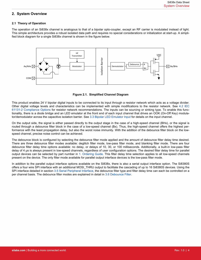
The operation of an Si838x channel is analogous to that of a bipolar opto-coupler, except an RF carrier is modulated instead of light.This simple architecture provides a robust isolated data path and requires no special considerations or initialization at start-up. A simpli-fied block diagram for a single Si838x channel is shown in the figure below.
Isol
atio
n Ba
rrie
r
Modulator
HFTransmitter
Demodulator
VDD
Ax/AHx Bx/BHx
COM
Debouncee B
BH
Figure 2.1. Simplified Channel Diagram
This product enables 24 V bipolar digital inputs to be connected to its input through a resistor network which acts as a voltage divider.Other digital voltage levels and characteristics can be implemented with simple modifications to the resistor network. See 4.2 IEC61131-2 Compliance Options for resistor network recommendations. The inputs can be sourcing or sinking type. To enable this func-tionality, there is a diode bridge and an LED emulator at the front end of each input channel that drives an OOK (On-Off Key) modula-tor/demodulator across the capacitive isolation barrier. See 3.3 Bipolar LED Emulator Input for details on the input channel.
On the output side, the signal is either passed directly to the output stage in the case of a high-speed channel (BHx), or the signal isrouted through a debounce filter block in the case of a low-speed channel (Bx). Thus, the high-speed channel offers the highest per-formance with the least propagation delay, but also the worst noise immunity. With the addition of the debounce filter block on the low-speed channel, precise noise control can be achieved.
The debounce block is configured by selecting the debounce filter mode applied and the amount of debounce filter delay time desired.There are three debounce filter modes available: deglitch filter mode, low-pass filter mode, and blanking filter mode. There are fourdebounce filter delay time options available: no delay, or delays of 10, 30, or 100 milliseconds. Additionally, a built-in low-pass filterdelay of 4 µs is always present in low-speed channels, regardless of user configuration options. The desired filter delay time for paralleloutput devices can be selected by part number in 1. Ordering Guide. This filter delay time selection applies to all low-speed channelspresent on the device. The only filter mode available for parallel output interface devices is the low-pass filter mode.
In addition to the parallel output interface options available on the Si838x, there is also a serial output interface option. The Si8380Soffers a four wire SPI interface with an additional MOSI_THRU output to facilitate the cascading of up to 16 Si8380S devices. Using theSPI interface detailed in section 3.5 Serial Peripheral Interface, the debounce filter type and filter delay time can each be controlled on aper channel basis. The debounce filter modes are explained in detail in 3.6 Debounce Filter.
Si838x Data SheetSystem Overview
silabs.com | Building a more connected world. Rev. 1.0 | 4
3. Device Operation
Table 3.1. Truth Table Summary
VDD Input, Ax/AHx Output, Bx/BHx
P1 ON HIGH
P OFF LOW
UP2 X Undetermined3
1. P = powered (> UVLO).2. UP = Unpowered (< UVLO).3. An undetermined state can be any value within the absolute maximum rating of the output channel. See Table 5.10 Absolute
Maximum Ratings1 on page 23 for details.
3.1 Device Behavior
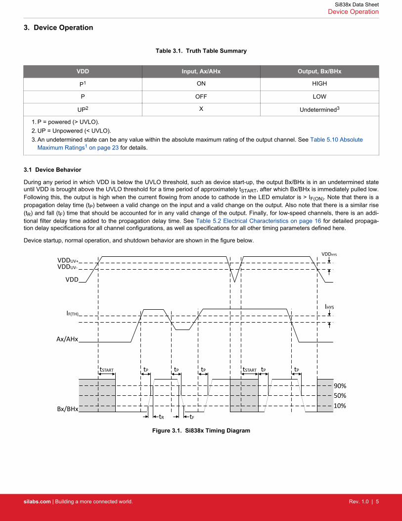
During any period in which VDD is below the UVLO threshold, such as device start-up, the output Bx/BHx is in an undetermined stateuntil VDD is brought above the UVLO threshold for a time period of approximately tSTART, after which Bx/BHx is immediately pulled low.Following this, the output is high when the current flowing from anode to cathode in the LED emulator is > IF(ON). Note that there is apropagation delay time (tP) between a valid change on the input and a valid change on the output. Also note that there is a similar rise(tR) and fall (tF) time that should be accounted for in any valid change of the output. Finally, for low-speed channels, there is an addi-tional filter delay time added to the propagation delay time. See Table 5.2 Electrical Characteristics on page 16 for detailed propaga-tion delay specifications for all channel configurations, as well as specifications for all other timing parameters defined here.
Device startup, normal operation, and shutdown behavior are shown in the figure below.
tR
tSTART tP
IHYSIF(TH)
Bx/BHx
VDD
VDDUV+VDDUV-
VDDHYS
tF
tP tP tSTART tP tP
10%50%90%
Ax/AHx
Figure 3.1. Si838x Timing Diagram
Si838x Data SheetDevice Operation
silabs.com | Building a more connected world. Rev. 1.0 | 5
3.2 Undervoltage Lockout
Undervoltage Lockout (UVLO) is provided to prevent erroneous operation during device startup and shutdown or when VDD is below itsspecified operating range. During UVLO, the outputs from the device do not track the inputs to the device. For example, the deviceunconditionally enters UVLO when VDD falls below VDDUV– and exits UVLO when VDD rises above VDDUV+. During UVLO, the out-puts are in an undetermined state and should be controlled using external components like a pull-up or pull-down resistor. See section3.4.2 Output Pin Termination and State Control for circuit recommendations
3.3 Bipolar LED Emulator Input
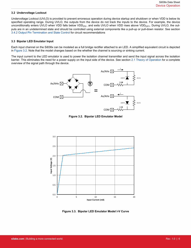
Each input channel on the Si838x can be modeled as a full bridge rectifier attached to an LED. A simplified equivalent circuit is depictedin Figure 3.2. Note that the model changes based on the whether the channel is sourcing or sinking current.
The input current to the LED emulator is used to power the isolation channel transmitter and send the input signal across the isolationbarrier. This eliminates the need for a power supply on the input side of the device. See section 2.1 Theory of Operation for a completeoverview of the signal path through the device.
Ax/AHx
COM
e
=
Ax/AHx
COM
2.0 V 3.1 k
21
I
Ax/AHx
COM
2.0 V 3.1 k
21
I
Figure 3.2. Bipolar LED Emulator Model
0.0
0.5
1.0
1.5
2.0
2.5
3.0
0 5 10 15 20
Inpu
t Vol
tage
(V)
Input Current (mA)
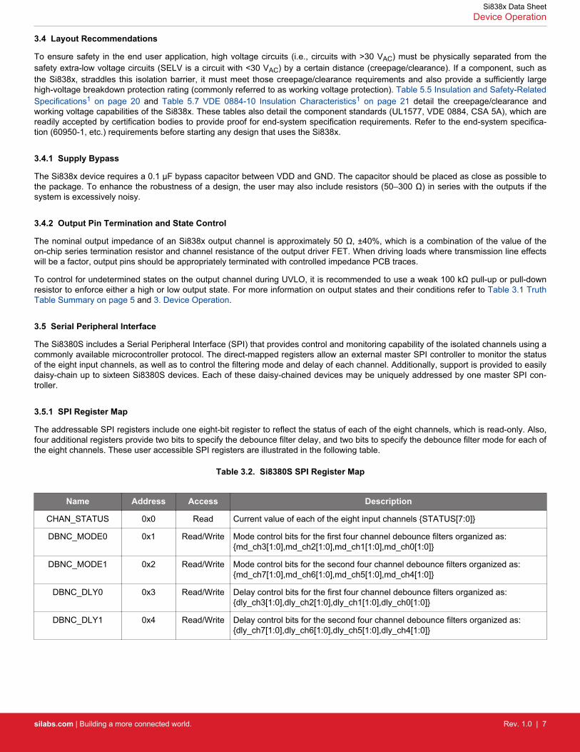
Figure 3.3. Bipolar LED Emulator Model I-V Curve
Si838x Data SheetDevice Operation
silabs.com | Building a more connected world. Rev. 1.0 | 6
3.4 Layout Recommendations
To ensure safety in the end user application, high voltage circuits (i.e., circuits with >30 VAC) must be physically separated from thesafety extra-low voltage circuits (SELV is a circuit with <30 VAC) by a certain distance (creepage/clearance). If a component, such asthe Si838x, straddles this isolation barrier, it must meet those creepage/clearance requirements and also provide a sufficiently largehigh-voltage breakdown protection rating (commonly referred to as working voltage protection). Table 5.5 Insulation and Safety-RelatedSpecifications1 on page 20 and Table 5.7 VDE 0884-10 Insulation Characteristics1 on page 21 detail the creepage/clearance andworking voltage capabilities of the Si838x. These tables also detail the component standards (UL1577, VDE 0884, CSA 5A), which arereadily accepted by certification bodies to provide proof for end-system specification requirements. Refer to the end-system specifica-tion (60950-1, etc.) requirements before starting any design that uses the Si838x.
3.4.1 Supply Bypass
The Si838x device requires a 0.1 µF bypass capacitor between VDD and GND. The capacitor should be placed as close as possible tothe package. To enhance the robustness of a design, the user may also include resistors (50–300 Ω) in series with the outputs if thesystem is excessively noisy.
3.4.2 Output Pin Termination and State Control
The nominal output impedance of an Si838x output channel is approximately 50 Ω, ±40%, which is a combination of the value of theon-chip series termination resistor and channel resistance of the output driver FET. When driving loads where transmission line effectswill be a factor, output pins should be appropriately terminated with controlled impedance PCB traces.
To control for undetermined states on the output channel during UVLO, it is recommended to use a weak 100 kΩ pull-up or pull-downresistor to enforce either a high or low output state. For more information on output states and their conditions refer to Table 3.1 TruthTable Summary on page 5 and 3. Device Operation.
3.5 Serial Peripheral Interface
The Si8380S includes a Serial Peripheral Interface (SPI) that provides control and monitoring capability of the isolated channels using acommonly available microcontroller protocol. The direct-mapped registers allow an external master SPI controller to monitor the statusof the eight input channels, as well as to control the filtering mode and delay of each channel. Additionally, support is provided to easilydaisy-chain up to sixteen Si8380S devices. Each of these daisy-chained devices may be uniquely addressed by one master SPI con-troller.
3.5.1 SPI Register Map
The addressable SPI registers include one eight-bit register to reflect the status of each of the eight channels, which is read-only. Also,four additional registers provide two bits to specify the debounce filter delay, and two bits to specify the debounce filter mode for each ofthe eight channels. These user accessible SPI registers are illustrated in the following table.
Table 3.2. Si8380S SPI Register Map
Name Address Access Description
CHAN_STATUS 0x0 Read Current value of each of the eight input channels STATUS[7:0]
DBNC_MODE0 0x1 Read/Write Mode control bits for the first four channel debounce filters organized as:md_ch3[1:0],md_ch2[1:0],md_ch1[1:0],md_ch0[1:0]
DBNC_MODE1 0x2 Read/Write Mode control bits for the second four channel debounce filters organized as:md_ch7[1:0],md_ch6[1:0],md_ch5[1:0],md_ch4[1:0]
DBNC_DLY0 0x3 Read/Write Delay control bits for the first four channel debounce filters organized as:dly_ch3[1:0],dly_ch2[1:0],dly_ch1[1:0],dly_ch0[1:0]
DBNC_DLY1 0x4 Read/Write Delay control bits for the second four channel debounce filters organized as:dly_ch7[1:0],dly_ch6[1:0],dly_ch5[1:0],dly_ch4[1:0]
Si838x Data SheetDevice Operation
silabs.com | Building a more connected world. Rev. 1.0 | 7
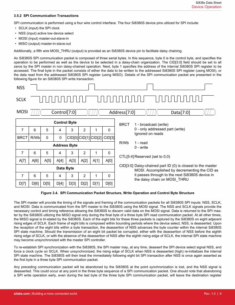
3.5.2 SPI Communication Transactions
SPI communication is performed using a four wire control interface. The four Si8380S device pins utilized for SPI include:• SCLK (input) the SPI clock• NSS (input) active low device select• MOSI (input) master-out-slave-in• MISO (output) master-in-slave-out
Additionally, a fifth wire MOSI_THRU (output) is provided as an Si8380S device pin to facilitate daisy chaining.
An Si8380S SPI communication packet is composed of three serial bytes. In this sequence, byte 0 is the control byte, and specifies theoperation to be performed as well as the device to be selected in a daisy-chain organization. The CID[3:0] field should be set to allzeros by the SPI master in non daisy-chained operation. Next, byte 1 specifies the address of the internal Si8380S SPI register to beaccessed. The final byte in the packet consists of either the data to be written to the addressed Si8380S SPI register (using MOSI), orthe data read from the addressed Si8380S SPI register (using MISO). Details of the SPI communication packet are presented in thefollowing figure for an Si8380S SPI write transaction.
NSS
SCLK
MOSI Control[7:0] Address[7:0] Data[7:0]
BRCT 1 - broadcast (write)0 - only addressed part (write)Ignored on reads
R/Wb 1 - read0 - write
CTL[5:4] Reserved (set to 0,0)
CID[3:0] Daisy-chained part ID (0) is closest to the masterMOSI. Accomplished by decrementing the CID asit passes through to the next Si8380S device in the daisy chain on MOSI_THRU
Control Byte
7 6 5 4 3 2 1 0
BRCT R/Wb 0 0 CID[0] CID[1] CID[2] CID[3]
Address Byte
7 6 5 4 3 2 1 0
A[7] A[6] A[5] A[4] A[3] A[2] A[1] A[0]
Data Byte
7 6 5 4 3 2 1 0
D[7] D[6] D[5] D[4] D[3] D[2] D[1] D[0]
Figure 3.4. SPI Communication Packet Structure, Write Operation and Control Byte Structure
The SPI master will provide the timing of the signals and framing of the communication packets for all Si8380S SPI inputs: NSS, SCLK,and MOSI. Data is communicated from the SPI master to the Si8380S using the MOSI signal. The NSS and SCLK signals provide thenecessary control and timing reference allowing the Si8380S to discern valid data on the MOSI signal. Data is returned to the SPI mas-ter by the Si8380S utilizing the MISO signal only during the final byte of a three byte SPI read communication packet. At all other times,the MISO signal is tri-stated by the Si8380S. Each of the eight bits for these three packets is captured by the Si8380S on eight adjacentrising edges of SCLK. Each frame of eight bits is composed within bounding periods where the device select, NSS, is deasserted. Uponthe reception of the eight bits within a byte transaction, the deassertion of NSS advances the byte counter within the internal Si8380SSPI state machine. Should the transmission of an eight bit packet be corrupted, either with the deassertion of NSS before the eighthrising edge of SCLK, or with the absence of the deassertion of NSS after the eighth rising edge of SCLK, the internal SPI state machinemay become unsynchronized with the master SPI controller.
To re-establish SPI synchronization with the Si8380S, the SPI master may, at any time, deassert the SPI device select signal NSS, andforce a clock cycle on SCLK. When unsynchronized, the rising edge of SCLK when NSS is deasserted (high) re-initializes the internalSPI state machine. The Si8380S will then treat the immediately following eight bit SPI transaction after NSS is once again asserted asthe first byte in a three byte SPI communication packet.
Any preceding communication packet will be abandoned by the Si8380S at the point synchronization is lost, and the NSS signal isdeasserted. This could occur at any point in the three byte sequence of a SPI communication packet. One should note that abandoninga SPI write operation early, even during the last byte of the three byte SPI communication packet, will leave the destination register
Si838x Data SheetDevice Operation
silabs.com | Building a more connected world. Rev. 1.0 | 8
unchanged. However, if the number of SCLK cycles exceeds eight during the last byte of the three byte SPI write packet, the destina-tion Si8380S register may be corrupted. To remedy both of these situations, it is recommended that such a corrupted write operation berepeated immediately following resynchronization of the SPI interface.
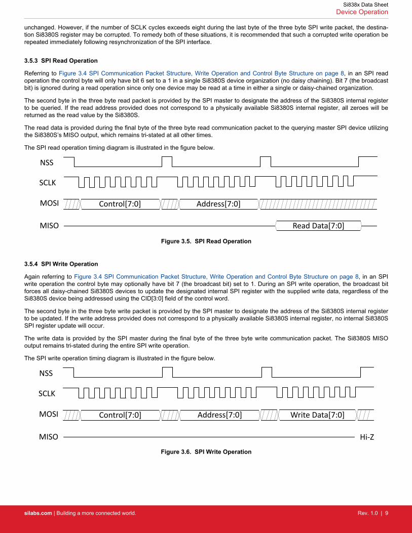
3.5.3 SPI Read Operation
Referring to Figure 3.4 SPI Communication Packet Structure, Write Operation and Control Byte Structure on page 8, in an SPI readoperation the control byte will only have bit 6 set to a 1 in a single Si8380S device organization (no daisy chaining). Bit 7 (the broadcastbit) is ignored during a read operation since only one device may be read at a time in either a single or daisy-chained organization.
The second byte in the three byte read packet is provided by the SPI master to designate the address of the Si8380S internal registerto be queried. If the read address provided does not correspond to a physically available Si8380S internal register, all zeroes will bereturned as the read value by the Si8380S.
The read data is provided during the final byte of the three byte read communication packet to the querying master SPI device utilizingthe Si8380S’s MISO output, which remains tri-stated at all other times.
The SPI read operation timing diagram is illustrated in the figure below.
NSS
SCLK
MOSI Control[7:0] Address[7:0]
Read Data[7:0]MISO
Figure 3.5. SPI Read Operation
3.5.4 SPI Write Operation
Again referring to Figure 3.4 SPI Communication Packet Structure, Write Operation and Control Byte Structure on page 8, in an SPIwrite operation the control byte may optionally have bit 7 (the broadcast bit) set to 1. During an SPI write operation, the broadcast bitforces all daisy-chained Si8380S devices to update the designated internal SPI register with the supplied write data, regardless of theSi8380S device being addressed using the CID[3:0] field of the control word.
The second byte in the three byte write packet is provided by the SPI master to designate the address of the Si8380S internal registerto be updated. If the write address provided does not correspond to a physically available Si8380S internal register, no internal Si8380SSPI register update will occur.
The write data is provided by the SPI master during the final byte of the three byte write communication packet. The Si8380S MISOoutput remains tri-stated during the entire SPI write operation.
The SPI write operation timing diagram is illustrated in the figure below.
NSS
SCLK
MOSI Control[7:0] Address[7:0]
MISO Hi-Z
Write Data[7:0]
Figure 3.6. SPI Write Operation
Si838x Data SheetDevice Operation
silabs.com | Building a more connected world. Rev. 1.0 | 9
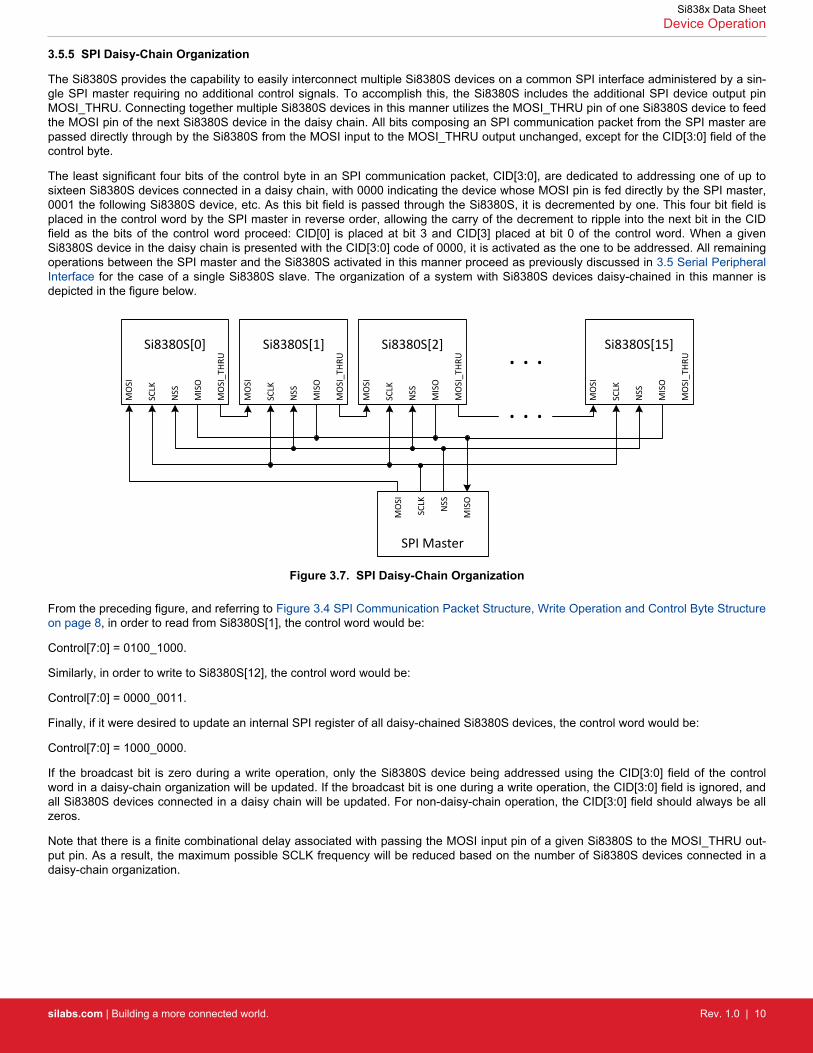
3.5.5 SPI Daisy-Chain Organization
The Si8380S provides the capability to easily interconnect multiple Si8380S devices on a common SPI interface administered by a sin-gle SPI master requiring no additional control signals. To accomplish this, the Si8380S includes the additional SPI device output pinMOSI_THRU. Connecting together multiple Si8380S devices in this manner utilizes the MOSI_THRU pin of one Si8380S device to feedthe MOSI pin of the next Si8380S device in the daisy chain. All bits composing an SPI communication packet from the SPI master arepassed directly through by the Si8380S from the MOSI input to the MOSI_THRU output unchanged, except for the CID[3:0] field of thecontrol byte.
The least significant four bits of the control byte in an SPI communication packet, CID[3:0], are dedicated to addressing one of up tosixteen Si8380S devices connected in a daisy chain, with 0000 indicating the device whose MOSI pin is fed directly by the SPI master,0001 the following Si8380S device, etc. As this bit field is passed through the Si8380S, it is decremented by one. This four bit field isplaced in the control word by the SPI master in reverse order, allowing the carry of the decrement to ripple into the next bit in the CIDfield as the bits of the control word proceed: CID[0] is placed at bit 3 and CID[3] placed at bit 0 of the control word. When a givenSi8380S device in the daisy chain is presented with the CID[3:0] code of 0000, it is activated as the one to be addressed. All remainingoperations between the SPI master and the Si8380S activated in this manner proceed as previously discussed in 3.5 Serial PeripheralInterface for the case of a single Si8380S slave. The organization of a system with Si8380S devices daisy-chained in this manner isdepicted in the figure below.
Si8380S[0]
MO
SI
SCLK
NSS
MIS
O
MO
SI_T
HRU
SPI Master
MO
SI
SCLK NSS
MIS
O
Si8380S[1]
MO
SI
SCLK
NSS
MIS
O
MO
SI_T
HRU
Si8380S[2]M
OSI
SCLK
NSS
MIS
O
MO
SI_T
HRU
Si8380S[15]
MO
SI
SCLK
NSS
MIS
O
MO
SI_T
HRU
. . .
. . .
Figure 3.7. SPI Daisy-Chain Organization
From the preceding figure, and referring to Figure 3.4 SPI Communication Packet Structure, Write Operation and Control Byte Structureon page 8, in order to read from Si8380S[1], the control word would be:
Control[7:0] = 0100_1000.
Similarly, in order to write to Si8380S[12], the control word would be:
Control[7:0] = 0000_0011.
Finally, if it were desired to update an internal SPI register of all daisy-chained Si8380S devices, the control word would be:
Control[7:0] = 1000_0000.
If the broadcast bit is zero during a write operation, only the Si8380S device being addressed using the CID[3:0] field of the controlword in a daisy-chain organization will be updated. If the broadcast bit is one during a write operation, the CID[3:0] field is ignored, andall Si8380S devices connected in a daisy chain will be updated. For non-daisy-chain operation, the CID[3:0] field should always be allzeros.
Note that there is a finite combinational delay associated with passing the MOSI input pin of a given Si8380S to the MOSI_THRU out-put pin. As a result, the maximum possible SCLK frequency will be reduced based on the number of Si8380S devices connected in adaisy-chain organization.
Si838x Data SheetDevice Operation
silabs.com | Building a more connected world. Rev. 1.0 | 10
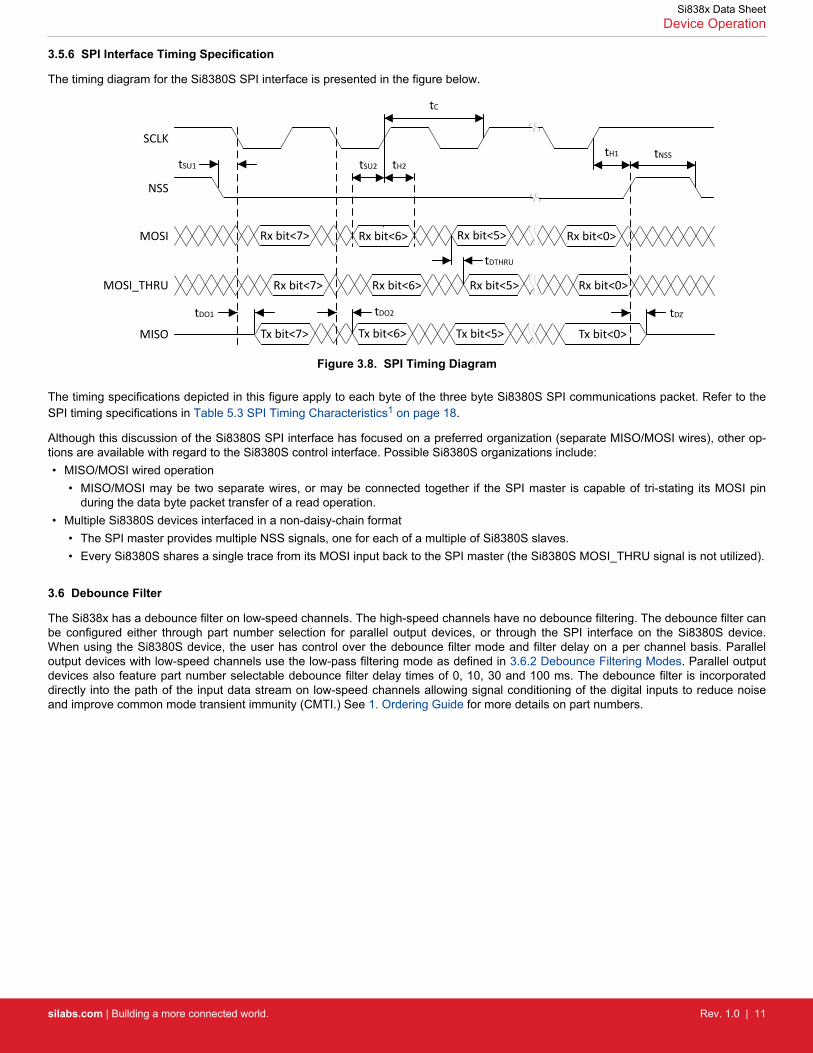
3.5.6 SPI Interface Timing Specification
The timing diagram for the Si8380S SPI interface is presented in the figure below.
NSS
MOSI
MOSI_THRU
MISO
SCLK
tDO1
tC
tDO2
tSU2 tH2tH1
tDZ
tSU1
Rx bit<7>
Rx bit<7>
Tx bit<7> Tx bit<6> Tx bit<5> Tx bit<0>
Rx bit<0>Rx bit<5>Rx bit<6>
Rx bit<0>Rx bit<5>Rx bit<6>
tNSS
tDTHRU
Figure 3.8. SPI Timing Diagram
The timing specifications depicted in this figure apply to each byte of the three byte Si8380S SPI communications packet. Refer to theSPI timing specifications in Table 5.3 SPI Timing Characteristics1 on page 18.
Although this discussion of the Si8380S SPI interface has focused on a preferred organization (separate MISO/MOSI wires), other op-tions are available with regard to the Si8380S control interface. Possible Si8380S organizations include:• MISO/MOSI wired operation
• MISO/MOSI may be two separate wires, or may be connected together if the SPI master is capable of tri-stating its MOSI pinduring the data byte packet transfer of a read operation.
• Multiple Si8380S devices interfaced in a non-daisy-chain format• The SPI master provides multiple NSS signals, one for each of a multiple of Si8380S slaves.• Every Si8380S shares a single trace from its MOSI input back to the SPI master (the Si8380S MOSI_THRU signal is not utilized).
3.6 Debounce Filter
The Si838x has a debounce filter on low-speed channels. The high-speed channels have no debounce filtering. The debounce filter canbe configured either through part number selection for parallel output devices, or through the SPI interface on the Si8380S device.When using the Si8380S device, the user has control over the debounce filter mode and filter delay on a per channel basis. Paralleloutput devices with low-speed channels use the low-pass filtering mode as defined in 3.6.2 Debounce Filtering Modes. Parallel outputdevices also feature part number selectable debounce filter delay times of 0, 10, 30 and 100 ms. The debounce filter is incorporateddirectly into the path of the input data stream on low-speed channels allowing signal conditioning of the digital inputs to reduce noiseand improve common mode transient immunity (CMTI.) See 1. Ordering Guide for more details on part numbers.
Si838x Data SheetDevice Operation
silabs.com | Building a more connected world. Rev. 1.0 | 11
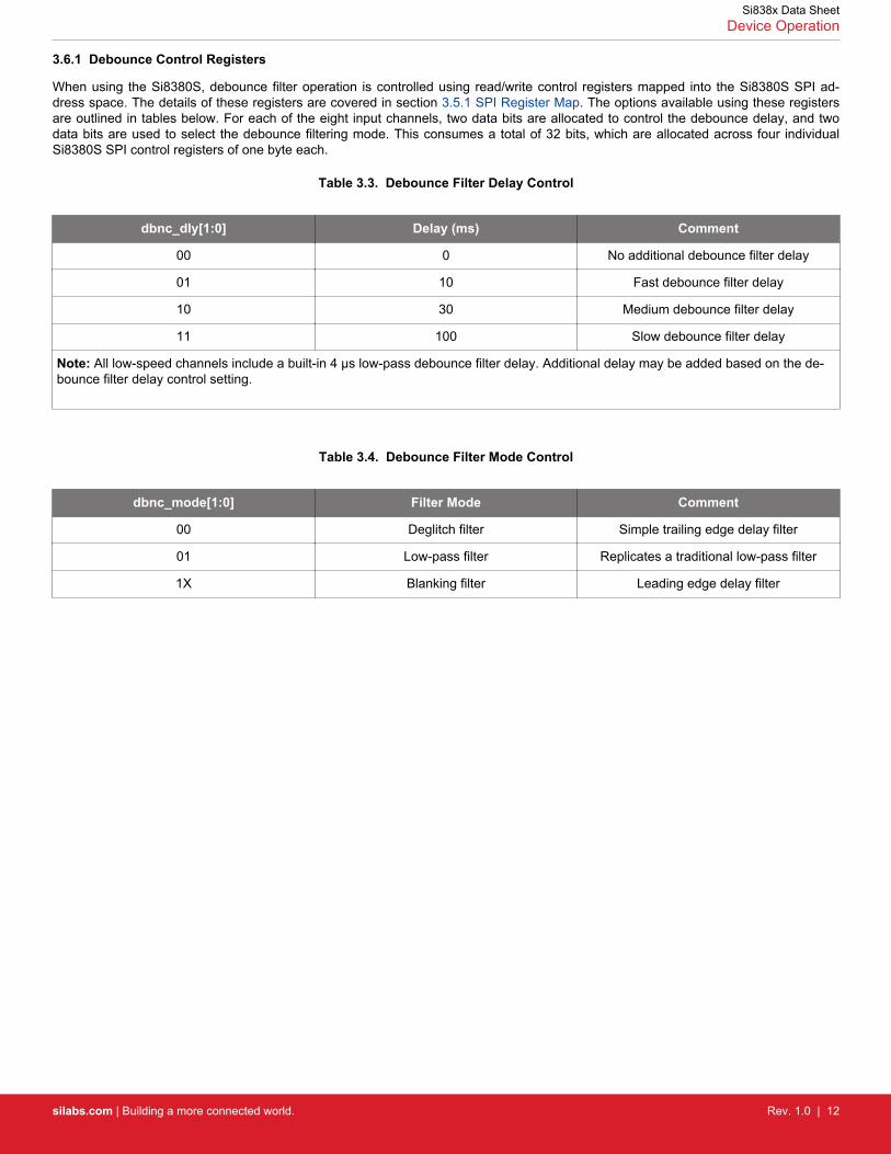
3.6.1 Debounce Control Registers
When using the Si8380S, debounce filter operation is controlled using read/write control registers mapped into the Si8380S SPI ad-dress space. The details of these registers are covered in section 3.5.1 SPI Register Map. The options available using these registersare outlined in tables below. For each of the eight input channels, two data bits are allocated to control the debounce delay, and twodata bits are used to select the debounce filtering mode. This consumes a total of 32 bits, which are allocated across four individualSi8380S SPI control registers of one byte each.
Table 3.3. Debounce Filter Delay Control
dbnc_dly[1:0] Delay (ms) Comment
00 0 No additional debounce filter delay
01 10 Fast debounce filter delay
10 30 Medium debounce filter delay
11 100 Slow debounce filter delay
Note: All low-speed channels include a built-in 4 µs low-pass debounce filter delay. Additional delay may be added based on the de-bounce filter delay control setting.
Table 3.4. Debounce Filter Mode Control
dbnc_mode[1:0] Filter Mode Comment
00 Deglitch filter Simple trailing edge delay filter
01 Low-pass filter Replicates a traditional low-pass filter
1X Blanking filter Leading edge delay filter
Si838x Data SheetDevice Operation
silabs.com | Building a more connected world. Rev. 1.0 | 12
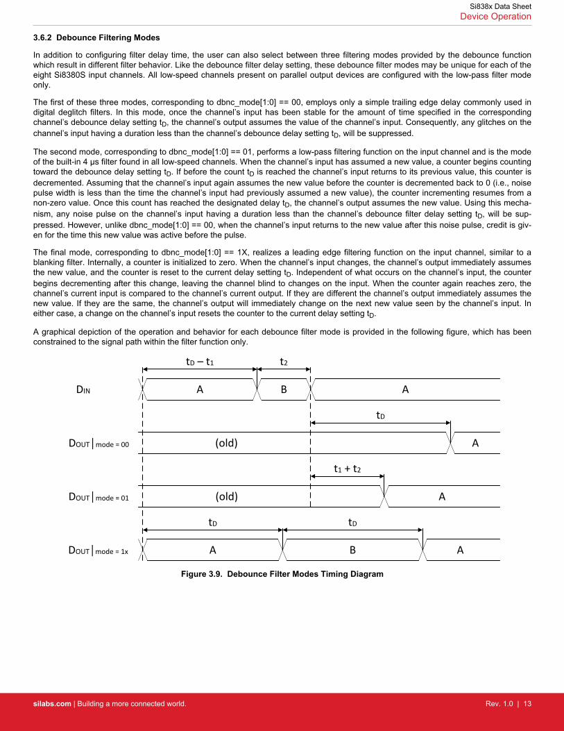
3.6.2 Debounce Filtering Modes
In addition to configuring filter delay time, the user can also select between three filtering modes provided by the debounce functionwhich result in different filter behavior. Like the debounce filter delay setting, these debounce filter modes may be unique for each of theeight Si8380S input channels. All low-speed channels present on parallel output devices are configured with the low-pass filter modeonly.
The first of these three modes, corresponding to dbnc_mode[1:0] == 00, employs only a simple trailing edge delay commonly used indigital deglitch filters. In this mode, once the channel’s input has been stable for the amount of time specified in the correspondingchannel’s debounce delay setting tD, the channel’s output assumes the value of the channel’s input. Consequently, any glitches on thechannel’s input having a duration less than the channel’s debounce delay setting tD, will be suppressed.
The second mode, corresponding to dbnc_mode[1:0] == 01, performs a low-pass filtering function on the input channel and is the modeof the built-in 4 µs filter found in all low-speed channels. When the channel’s input has assumed a new value, a counter begins countingtoward the debounce delay setting tD. If before the count tD is reached the channel’s input returns to its previous value, this counter isdecremented. Assuming that the channel’s input again assumes the new value before the counter is decremented back to 0 (i.e., noisepulse width is less than the time the channel’s input had previously assumed a new value), the counter incrementing resumes from anon-zero value. Once this count has reached the designated delay tD, the channel’s output assumes the new value. Using this mecha-nism, any noise pulse on the channel’s input having a duration less than the channel’s debounce filter delay setting tD, will be sup-pressed. However, unlike dbnc_mode[1:0] == 00, when the channel’s input returns to the new value after this noise pulse, credit is giv-en for the time this new value was active before the pulse.
The final mode, corresponding to dbnc_mode[1:0] == 1X, realizes a leading edge filtering function on the input channel, similar to ablanking filter. Internally, a counter is initialized to zero. When the channel’s input changes, the channel’s output immediately assumesthe new value, and the counter is reset to the current delay setting tD. Independent of what occurs on the channel’s input, the counterbegins decrementing after this change, leaving the channel blind to changes on the input. When the counter again reaches zero, thechannel’s current input is compared to the channel’s current output. If they are different the channel’s output immediately assumes thenew value. If they are the same, the channel’s output will immediately change on the next new value seen by the channel’s input. Ineither case, a change on the channel’s input resets the counter to the current delay setting tD.
A graphical depiction of the operation and behavior for each debounce filter mode is provided in the following figure, which has beenconstrained to the signal path within the filter function only.
A B ADOUTmode = 1x
tD tD
DOUTmode = 01 (old) A
t1 + t2
DOUTmode = 00 (old) A
tD
A B ADIN
t2tD – t1
Figure 3.9. Debounce Filter Modes Timing Diagram
Si838x Data SheetDevice Operation
silabs.com | Building a more connected world. Rev. 1.0 | 13
4. Applications
4.1 System Level Transitions
Si838xP
2.2nF
Low-sideResistor
High-sideResistor AHx
InputBHx
Output
COM GND
VDD
R1
R2
VD
Field Potential
IIN
IDC1
24V DC
uController
Input
GND
VDDVIN
Field PLC Digital Input Module PLC
High-Speed Channels Only
SensorOr Switch
Isol
atio
n Ba
rrie
r
Current Limit
Resistor
Status Lamp LED
R3
D2
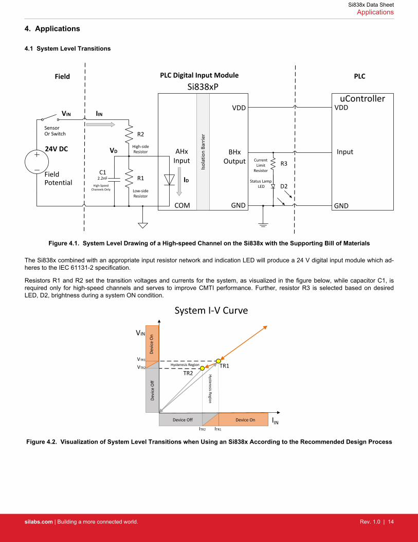
Figure 4.1. System Level Drawing of a High-speed Channel on the Si838x with the Supporting Bill of Materials
The Si838x combined with an appropriate input resistor network and indication LED will produce a 24 V digital input module which ad-heres to the IEC 61131-2 specification.
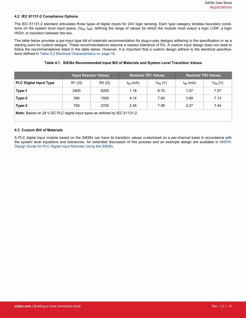
Resistors R1 and R2 set the transition voltages and currents for the system, as visualized in the figure below, while capacitor C1, isrequired only for high-speed channels and serves to improve CMTI performance. Further, resistor R3 is selected based on desiredLED, D2, brightness during a system ON condition.
VIN
IIN
TR1
Device On
System I-V Curve
TR2
Devi
ce O
n
VTR1
VTR2
Device Off
Devi
ce O
ff
Hysteresis Region
Hysteresis Region
ITR1ITR2
Figure 4.2. Visualization of System Level Transitions when Using an Si838x According to the Recommended Design Process
Si838x Data SheetApplications
silabs.com | Building a more connected world. Rev. 1.0 | 14
4.2 IEC 61131-2 Compliance Options
The IEC 61131-2 standard articulates three types of digital inputs for 24V logic sensing. Each type category dictates boundary condi-tions on the system level input space, (VIN, IIN), defining the range of values for which the module must output a logic LOW, a logicHIGH, or transition between the two.
The table below provides a per-input type bill of materials recommendation for plug-n-play designs adhering to the specification or as astarting point for custom designs. These recommendations assume a resistor tolerance of 5%. A custom input design does not need tofollow the recommendations listed in the table below. However, it is important that a custom design adhere to the electrical specifica-tions defined in Table 5.2 Electrical Characteristics on page 16.
Table 4.1. Si838x Recommended Input Bill of Materials and System Level Transition Values
Input Resistor Values Nominal TR1 Values Nominal TR2 Values
PLC Digital Input Type R1 (Ω) R2 (Ω) IIN (mA) VIN (V) IIN (mA) VIN (V)
Type-1 2400 6200 1.18 8.70 1.07 7.97
Type-2 390 1500 4.14 7.60 3.88 7.13
Type-3 750 2700 2.45 7.98 2.27 7.44
Note: Based on 24 V DC PLC digital input types as defined by IEC 61131-2.
4.3 Custom Bill of Materials
A PLC digital input module based on the Si838x can have its transition values customized on a per-channel basis in accordance withthe system level equations and tolerances. An extended discussion of this process and an example design are available in AN970:Design Guide for PLC Digital Input Modules Using the Si838x.
Si838x Data SheetApplications
silabs.com | Building a more connected world. Rev. 1.0 | 15
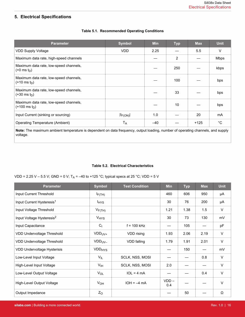
5. Electrical Specifications
Table 5.1. Recommended Operating Conditions
Parameter Symbol Min Typ Max Unit
VDD Supply Voltage VDD 2.25 — 5.5 V
Maximum data rate, high-speed channels — 2 — Mbps
Maximum data rate, low-speed channels,(+0 ms tD) — 250 — kbps
Maximum data rate, low-speed channels,(+10 ms tD) — 100 — bps
Maximum data rate, low-speed channels,(+30 ms tD) — 33 — bps
Maximum data rate, low-speed channels,(+100 ms tD) — 10 — bps
Input Current (sinking or sourcing) |IF(ON)| 1.0 — 20 mA
Operating Temperature (Ambient) TA –40 — +125 °C
Note: The maximum ambient temperature is dependent on data frequency, output loading, number of operating channels, and supplyvoltage.
Table 5.2. Electrical Characteristics
VDD = 2.25 V – 5.5 V; GND = 0 V; TA = –40 to +125 °C; typical specs at 25 °C; VDD = 5 V
Parameter Symbol Test Condition Min Typ Max Unit
Input Current Threshold IF(TH) 460 606 950 µA
Input Current Hysteresis1 IHYS 30 76 200 µA
Input Voltage Threshold VF(TH) 1.21 1.38 1.5 V
Input Voltage Hysteresis2 VHYS 30 73 130 mV
Input Capacitance CI f = 100 kHz — 105 — pF
VDD Undervoltage Threshold VDDUV+ VDD rising 1.93 2.06 2.19 V
VDD Undervoltage Threshold VDDUV– VDD falling 1.79 1.91 2.01 V
VDD Undervoltage Hysterisis VDDHYS — 150 — mV
Low-Level Input Voltage VIL SCLK, NSS, MOSI — — 0.8 V
High-Level Input Voltage VIH SCLK, NSS, MOSI 2.0 — — V
Low-Level Output Voltage VOL IOL = 4 mA — — 0.4 V
High-Level Output Voltage VOH IOH = –4 mA VDD –0.4 — — V
Output Impedance ZO — 50 — Ω
Si838x Data SheetElectrical Specifications
silabs.com | Building a more connected world. Rev. 1.0 | 16
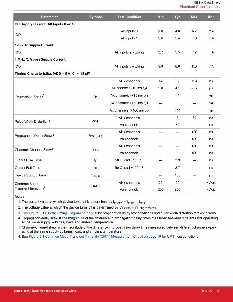
Parameter Symbol Test Condition Min Typ Max Unit
DC Supply Current (All Inputs 0 or 1)
IDDAll inputs 0 2.8 4.8 6.7 mA
All inputs 1 3.6 5.4 7.6 mA
125 kHz Supply Current
IDD All inputs switching 3.7 5.5 7.7 mA
1 MHz (2 Mbps) Supply Current
IDD All inputs switching 3.9 5.6 8.0 mA
Timing Characteristics (VDD = 5 V, CL = 15 pF)
Propagation Delay3 tP
AHx channels 47 82 124 ns
Ax channels (+0 ms tD) 3.8 4.1 4.6 µs
Ax channels (+10 ms tD) — 10 — ms
Ax channels (+30 ms tD) — 30 — ms
Ax channels (+100 ms tD) — 100 — ms
Pulse Width Distortion3 PWDAHx channels — 6 50 ns
Ax channels — 80 — ns
Propagation Delay Skew4 tPSK(P-P)AHx channels — — ±30 ns
Ax channels — — ±80 ns
Channel–Channel Skew5 tPSKAHx channels — — ±30 ns
Ax channels — — ±80 ns
Output Rise Time tR 50 Ω load +100 pF — 3.9 — ns
Output Fall Time tF 50 Ω load +100 pF — 3.7 — ns
Device Startup Time tSTART — 150 — µs
Common Mode Transient Immunity6 CMTI
AHx channels 25 50 — kV/µs
Ax channels 200 300 — kV/µs
Notes:1. The current value at which device turns off is determined by IF(OFF) = IF(TH) – IHYS.2. The voltage value at which the device turns off is determined by VF(OFF) = VF(TH) – VHYS.3. See Figure 3.1 Si838x Timing Diagram on page 5 for propagation delay test conditions and pulse width distortion test conditions.4. Propagation delay skew is the magnitude of the difference in propagation delay times measured between different units operating
at the same supply voltages, load, and ambient temperature.5. Channel-channel skew is the magnitude of the difference in propagation delay times measured between different channels oper-
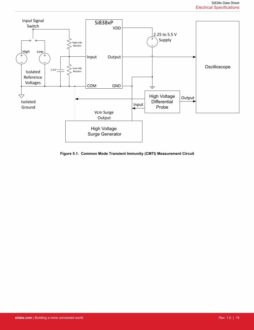
ating at the same supply voltages, load, and ambient temperature.6. See Figure 5.1 Common Mode Transient Immunity (CMTI) Measurement Circuit on page 19 for CMTI test conditions.
Si838x Data SheetElectrical Specifications
silabs.com | Building a more connected world. Rev. 1.0 | 17
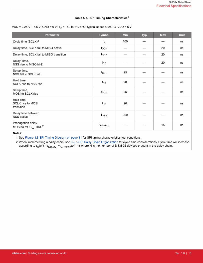
Table 5.3. SPI Timing Characteristics1
VDD = 2.25 V – 5.5 V; GND = 0 V; TA = –40 to +125 °C; typical specs at 25 °C; VDD = 5 V
Parameter Symbol Min Typ Max Unit
Cycle time (SCLK)2 tC 100 — — ns
Delay time, SCLK fall to MISO active tDO1 — — 20 ns
Delay time, SCLK fall to MISO transition tDO2 — — 20 ns
Delay Time, NSS rise to MISO hi-Z
tDZ — — 20 ns
Setup time, NSS fall to SCLK fall
tSU1 25 — — ns
Hold time, SCLK rise to NSS rise
tH1 20 — — ns
Setup time, MOSI to SCLK rise
tSU2 25 — — ns
Hold time, SCLK rise to MOSI transition
tH2 20 — — ns
Delay time betweenNSS active
tNSS 200 — — ns
Propagation delay,MOSI to MOSI_THRU2 tDTHRU — — 15 ns
Notes:1. See Figure 3.8 SPI Timing Diagram on page 11 for SPI timing characteristics test conditions.2. When implementing a daisy chain, see 3.5.5 SPI Daisy-Chain Organization for cycle time considerations. Cycle time will increase
according to tC(N ) = tC(MIN ) + tDTHRU (N - 1) where N is the number of Si8380S devices present in the daisy chain.
Si838x Data SheetElectrical Specifications
silabs.com | Building a more connected world. Rev. 1.0 | 18
OscilloscopeIsolated
Reference Voltages
Si838xP
2.25 to 5.5 VSupply
High Voltage Surge Generator
Vcm SurgeOutput
High Voltage Differential
Probe
Input SignalSwitch
InputOutput
Isolated Ground
2.2nF Low-sideResistor
High-sideResistor
High LowInput Output
COM GND
VDD
Figure 5.1. Common Mode Transient Immunity (CMTI) Measurement Circuit
Si838x Data SheetElectrical Specifications
silabs.com | Building a more connected world. Rev. 1.0 | 19
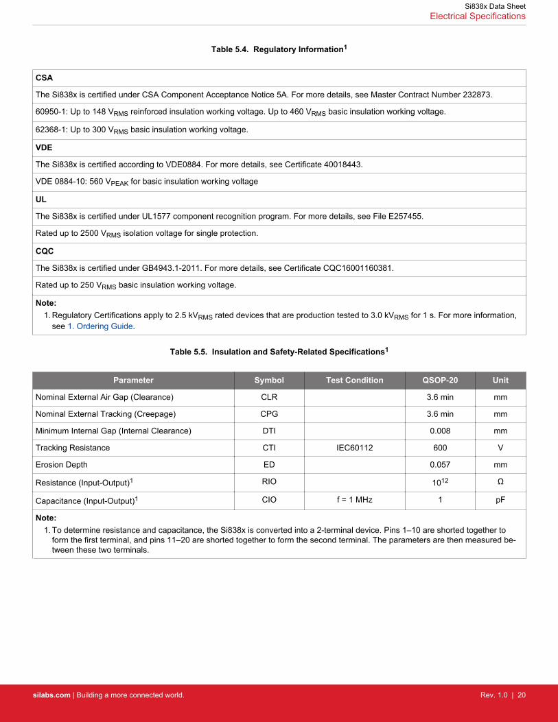
Table 5.4. Regulatory Information1
CSA
The Si838x is certified under CSA Component Acceptance Notice 5A. For more details, see Master Contract Number 232873.
60950-1: Up to 148 VRMS reinforced insulation working voltage. Up to 460 VRMS basic insulation working voltage.
62368-1: Up to 300 VRMS basic insulation working voltage.
VDE
The Si838x is certified according to VDE0884. For more details, see Certificate 40018443.
VDE 0884-10: 560 VPEAK for basic insulation working voltage
UL
The Si838x is certified under UL1577 component recognition program. For more details, see File E257455.
Rated up to 2500 VRMS isolation voltage for single protection.
CQC
The Si838x is certified under GB4943.1-2011. For more details, see Certificate CQC16001160381.
Rated up to 250 VRMS basic insulation working voltage.
Note:1. Regulatory Certifications apply to 2.5 kVRMS rated devices that are production tested to 3.0 kVRMS for 1 s. For more information,
see 1. Ordering Guide.
Table 5.5. Insulation and Safety-Related Specifications1
Parameter Symbol Test Condition QSOP-20 Unit
Nominal External Air Gap (Clearance) CLR 3.6 min mm
Nominal External Tracking (Creepage) CPG 3.6 min mm
Minimum Internal Gap (Internal Clearance) DTI 0.008 mm
Tracking Resistance CTI IEC60112 600 V
Erosion Depth ED 0.057 mm
Resistance (Input-Output)1 RIO 1012 Ω
Capacitance (Input-Output)1 CIO f = 1 MHz 1 pF
Note:1. To determine resistance and capacitance, the Si838x is converted into a 2-terminal device. Pins 1–10 are shorted together to
form the first terminal, and pins 11–20 are shorted together to form the second terminal. The parameters are then measured be-tween these two terminals.
Si838x Data SheetElectrical Specifications
silabs.com | Building a more connected world. Rev. 1.0 | 20
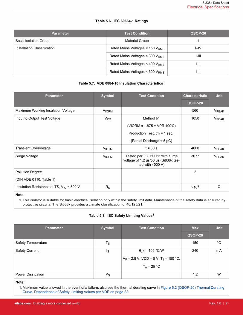
Table 5.6. IEC 60664-1 Ratings
Parameter Test Condition QSOP-20
Basic Isolation Group Material Group I
Installation Classification Rated Mains Voltages < 150 VRMS I–IV
Rated Mains Voltages < 300 VRMS I-III
Rated Mains Voltages < 400 VRMS I-II
Rated Mains Voltages < 600 VRMS I-II
Table 5.7. VDE 0884-10 Insulation Characteristics1
Parameter Symbol Test Condition Characteristic Unit
QSOP-20
Maximum Working Insulation Voltage VIORM 560 VPEAK
Input to Output Test Voltage VPR Method b1
(VIORM x 1.875 = VPR,100%)
Production Test, tm = 1 sec,
(Partial Discharge < 5 pC)
1050 VPEAK
Transient Overvoltage VIOTM t = 60 s 4000 VPEAK
Surge Voltage VIOSM Tested per IEC 60065 with surgevoltage of 1.2 µs/50 µs (Si838x tes-
ted with 4000 V)
3077 VPEAK
Pollution Degree
(DIN VDE 0110, Table 1)
2
Insulation Resistance at TS, VIO = 500 V RS >109 Ω
Note:1. This isolator is suitable for basic electrical isolation only within the safety limit data. Maintenance of the safety data is ensured by
protective circuits. The Si838x provides a climate classification of 40/125/21.
Table 5.8. IEC Safety Limiting Values1
Parameter Symbol Test Condition Max Unit
QSOP-20
Safety Temperature TS 150 °C
Safety Current IS θJA = 105 °C/W
VF = 2.8 V, VDD = 5 V, TJ = 150 °C,
TA = 25 °C
240 mA
Power Dissipation PS 1.2 W
Note:1. Maximum value allowed in the event of a failure; also see the thermal derating curve in Figure 5.2 (QSOP-20) Thermal Derating
Curve, Dependence of Safety Limiting Values per VDE on page 22.
Si838x Data SheetElectrical Specifications
silabs.com | Building a more connected world. Rev. 1.0 | 21
Table 5.9. Thermal Characteristics
Parameter Symbol QSOP-20 Unit
IC Junction-to-Ambient Thermal Resistance θJA 105 °C/W
0
120
240
360
480
600
0 40 80 120 160
Safe
ty L
imiti
ng C
urre
nt (m
A)
Ambient Temperature (°C)
VDD = 2.5 V
VDD = 3.3 V
VDD = 5.0 V
Figure 5.2. (QSOP-20) Thermal Derating Curve, Dependence of Safety Limiting Values per VDE
Si838x Data SheetElectrical Specifications
silabs.com | Building a more connected world. Rev. 1.0 | 22
Table 5.10. Absolute Maximum Ratings1
Parameter Symbol Min Max Unit
Storage Temperature TSTG –65 +150 °C
Ambient Temperature TA –40 +125 °C
Junction Temperature TJ — +150 °C
Average Forward Input Current IF(AVG) — 30 mA
Peak Transient Input Current (< 1 µs pulse width, 300 ps)
IFTR — 1 A
Supply Voltage VDD –0.5 7 V
Output Voltage VOUT –0.5 VDD+0.5 V
Average Output Current IO(AVG) — 10 mA
Input Power Dissipation PI — 480 mW
Output Power Dissipation (includes 3 mA per channel forstatus LED)
PO — 484 mW
Total Power Dissipation PT — 964 mW
Lead Solder Temperature (10 s) — 260 °C
HBM Rating ESD 4 — kV
Machine Model ESD 200 — V
CDM 500 — V
Maximum Isolation Voltage (1 s) — 3000 VRMS
Note:1. Permanent device damage may occur if the absolute maximum ratings are exceeded. Functional operation should be restricted to
the conditions specified in the operational sections of this data sheet.
Si838x Data SheetElectrical Specifications
silabs.com | Building a more connected world. Rev. 1.0 | 23
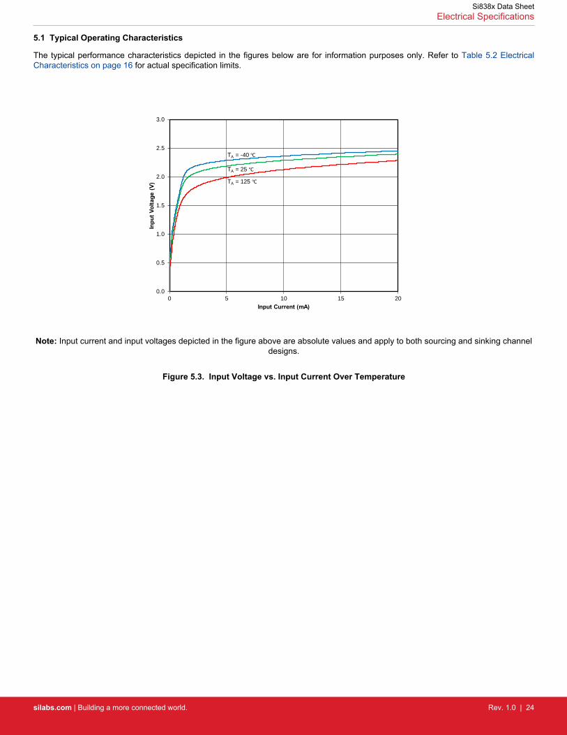
5.1 Typical Operating Characteristics
The typical performance characteristics depicted in the figures below are for information purposes only. Refer to Table 5.2 ElectricalCharacteristics on page 16 for actual specification limits.
0.0
0.5
1.0
1.5
2.0
2.5
3.0
0 5 10 15 20
Inpu
t Vol
tage
(V)
Input Current (mA)
TA = -40 °C
TA = 25 °C
TA = 125 °C
Note: Input current and input voltages depicted in the figure above are absolute values and apply to both sourcing and sinking channeldesigns.
Figure 5.3. Input Voltage vs. Input Current Over Temperature
Si838x Data SheetElectrical Specifications
silabs.com | Building a more connected world. Rev. 1.0 | 24
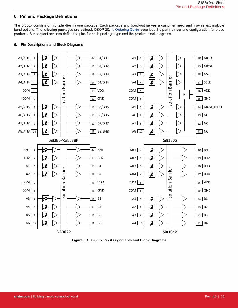
6. Pin and Package Definitions
The Si838x consists of multiple dies in one package. Each package and bond-out serves a customer need and may reflect multiplebond options. The following packages are defined: QSOP-20. 1. Ordering Guide describes the part number and configuration for theseproducts. Subsequent sections define the pins for each package type and the product block diagrams.
6.1 Pin Descriptions and Block Diagrams
AH2 AH2
AH3
AH4
A3
A4
A1
A2
1
2
3
4
5
6
9
10
19
18
17
16
15
A1/AH1
A2/AH2
A3/AH3
A4/AH4
COM
COM
A7/AH7
A8/AH8
B1/BH1
B2/BH2
B3/BH3
B4/BH4
VDD
GND
B7/BH7
B8/BH8
7
8
A5/AH5
A6/AH6
B5/BH5
B6/BH6
Si8380P/Si8388P
14
12
11
20
13
e
e
e
e
e
e
e
e
Isol
atio
n Ba
rrie
r
1
2
3
4
5
6
9
10
19
18
17
16
15
AH1
A1
A2
COM
COM
A5
A6
BH1
BH2
B1
B2
VDD
GND
B5
B6
7
8
A3
A4
B3
B4
Si8382P
14
12
11
20
13
e
e
e
e
e
e
e
e
Isol
atio
n Ba
rrie
r
1
2
3
4
5
6
9
10
19
18
17
16
15
AH1
COM
COM
BH1
BH2
BH3
BH4
VDD
GND
B3
B4
7
8
B1
B2
Si8384P
14
12
11
20
13
e
e
e
e
e
e
e
e
Isol
atio
n Ba
rrie
r
1
2
3
4
5
6
9
10
19
18
17
16
15
A1
A2
A3
A4
COM
COM
A7
A8
MISO
MOSI
NSS
SCLK
VDD
GND
NC
NC
7
8
A5
A6
MOSI_THRU
NC
Si8380S
14
12
11
20
13
Isol
atio
n Ba
rrie
r
SPI
e
e
e
e
e
e
e
e
Figure 6.1. Si838x Pin Assignments and Block Diagrams
Si838x Data SheetPin and Package Definitions
silabs.com | Building a more connected world. Rev. 1.0 | 25
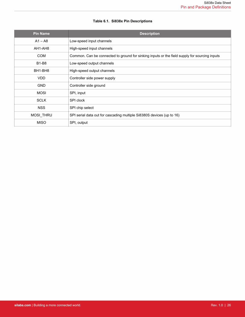
Table 6.1. Si838x Pin Descriptions
Pin Name Description
A1 – A8 Low-speed input channels
AH1-AH8 High-speed input channels
COM Common. Can be connected to ground for sinking inputs or the field supply for sourcing inputs
B1-B8 Low-speed output channels
BH1-BH8 High-speed output channels
VDD Controller side power supply
GND Controller side ground
MOSI SPI, input
SCLK SPI clock
NSS SPI chip select
MOSI_THRU SPI serial data out for cascading multiple Si8380S devices (up to 16)
MISO SPI, output
Si838x Data SheetPin and Package Definitions
silabs.com | Building a more connected world. Rev. 1.0 | 26
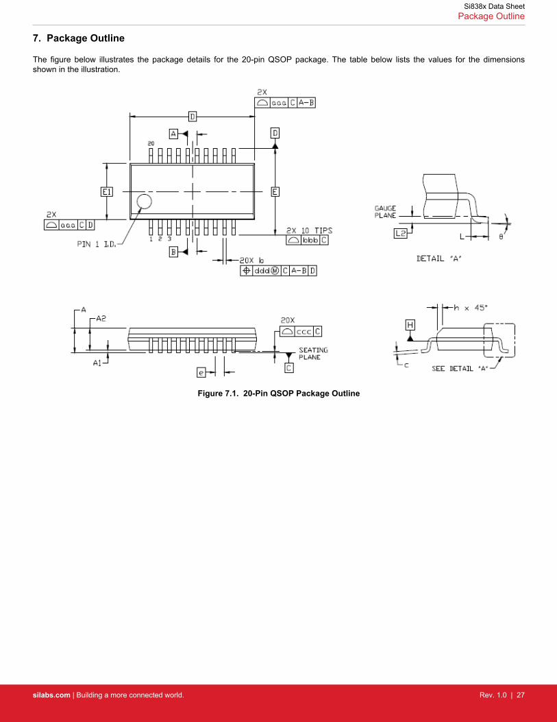
7. Package Outline
The figure below illustrates the package details for the 20-pin QSOP package. The table below lists the values for the dimensionsshown in the illustration.
Figure 7.1. 20-Pin QSOP Package Outline
Si838x Data SheetPackage Outline
silabs.com | Building a more connected world. Rev. 1.0 | 27
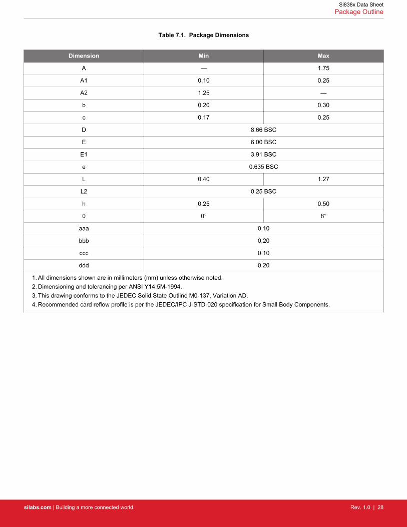
Table 7.1. Package Dimensions
Dimension Min Max
A — 1.75
A1 0.10 0.25
A2 1.25 —
b 0.20 0.30
c 0.17 0.25
D 8.66 BSC
E 6.00 BSC
E1 3.91 BSC
e 0.635 BSC
L 0.40 1.27
L2 0.25 BSC
h 0.25 0.50
θ 0° 8°
aaa 0.10
bbb 0.20
ccc 0.10
ddd 0.20
1. All dimensions shown are in millimeters (mm) unless otherwise noted.2. Dimensioning and tolerancing per ANSI Y14.5M-1994.3. This drawing conforms to the JEDEC Solid State Outline M0-137, Variation AD.4. Recommended card reflow profile is per the JEDEC/IPC J-STD-020 specification for Small Body Components.
Si838x Data SheetPackage Outline
silabs.com | Building a more connected world. Rev. 1.0 | 28
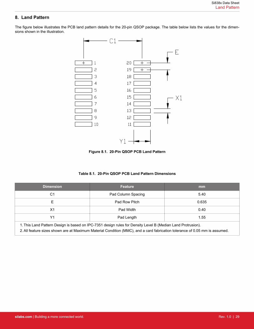
8. Land Pattern
The figure below illustrates the PCB land pattern details for the 20-pin QSOP package. The table below lists the values for the dimen-sions shown in the illustration.
Figure 8.1. 20-Pin QSOP PCB Land Pattern
Table 8.1. 20-Pin QSOP PCB Land Pattern Dimensions
Dimension Feature mm
C1 Pad Column Spacing 5.40
E Pad Row Pitch 0.635
X1 Pad Width 0.40
Y1 Pad Length 1.55
1. This Land Pattern Design is based on IPC-7351 design rules for Density Level B (Median Land Protrusion).2. All feature sizes shown are at Maximum Material Condition (MMC), and a card fabrication tolerance of 0.05 mm is assumed.
Si838x Data SheetLand Pattern
silabs.com | Building a more connected world. Rev. 1.0 | 29
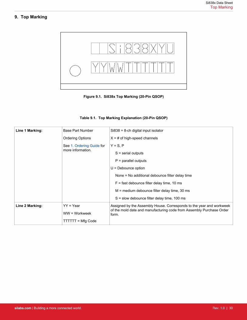
9. Top Marking
Figure 9.1. Si838x Top Marking (20-Pin QSOP)
Table 9.1. Top Marking Explanation (20-Pin QSOP)
Line 1 Marking: Base Part Number
Ordering Options
See 1. Ordering Guide formore information.
Si838 = 8-ch digital input isolator
X = # of high-speed channels
Y = S, P
S = serial outputs
P = parallel outputs
U = Debounce option
None = No additional debounce filter delay time
F = fast debounce filter delay time, 10 ms
M = medium debounce filter delay time, 30 ms
S = slow debounce filter delay time, 100 ms
Line 2 Marking: YY = Year
WW = Workweek
TTTTTT = Mfg Code
Assigned by the Assembly House. Corresponds to the year and workweekof the mold date and manufacturing code from Assembly Purchase Orderform.
Si838x Data SheetTop Marking
silabs.com | Building a more connected world. Rev. 1.0 | 30
10. Revision History
Revision 1.0
April, 2019• Reorganized document to improve readability• Updated content throughout the data sheet to improve readability, matched style guidelines, and corrected minor grammatical errors• Corrected the output state when device is unpowered in Table 3.1 Truth Table Summary on page 5• Added 3.3 Bipolar LED Emulator Input to improve input channel design documentation• Added recommendation to control output states to 3.4.2 Output Pin Termination and State Control• Removed redundant specifications, added details and notes, and reorganized 5. Electrical Specifications• Added Input Voltage specifications to Table 5.2 Electrical Characteristics on page 16• Expanded and clarified Propagation Delay specifications in Table 5.2 Electrical Characteristics on page 16• Expanded and clarified Propagation Delay specifications in Table 5.2 Electrical Characteristics on page 16• Defined capacitive load in test conditions for rise and fall time in Table 5.2 Electrical Characteristics on page 16• Updated Table 5.4 Regulatory Information1 on page 20 to reflect latest certification status• Added surge voltage specification to Table 5.7 VDE 0884-10 Insulation Characteristics1 on page 21• Corrected Safety Current specification in 4.2 IEC 61131-2 Compliance Options• Corrected plot in Figure 5.2 (QSOP-20) Thermal Derating Curve, Dependence of Safety Limiting Values per VDE on page 22• Removed input voltage parameter from Table 5.10 Absolute Maximum Ratings1 on page 23• Updated plot in Figure 5.3 Input Voltage vs. Input Current Over Temperature on page 24• Corrected Line 1 Marking in Table 9.1 Top Marking Explanation (20-Pin QSOP) on page 30
Revision 0.5
April, 2016• Initial release.
Si838x Data SheetRevision History
silabs.com | Building a more connected world. Rev. 1.0 | 31

Smart. Connected. Energy-Friendly.
Productswww.silabs.com/products
Qualitywww.silabs.com/quality
Support and Communitycommunity.silabs.com
http://www.silabs.com
Silicon Laboratories Inc.400 West Cesar ChavezAustin, TX 78701USA
DisclaimerSilicon Labs intends to provide customers with the latest, accurate, and in-depth documentation of all peripherals and modules available for system and software implementers using or intending to use the Silicon Labs products. Characterization data, available modules and peripherals, memory sizes and memory addresses refer to each specific device, and "Typical" parameters provided can and do vary in different applications. Application examples described herein are for illustrative purposes only. Silicon Labs reserves the right to make changes without further notice to the product information, specifications, and descriptions herein, and does not give warranties as to the accuracy or completeness of the included information. Without prior notification, Silicon Labs may update product firmware during the manufacturing process for security or reliability reasons. Such changes will not alter the specifications or the performance of the product. Silicon Labs shall have no liability for the consequences of use of the information supplied in this document. This document does not imply or expressly grant any license to design or fabricate any integrated circuits. The products are not designed or authorized to be used within any FDA Class III devices, applications for which FDA premarket approval is required or Life Support Systems without the specific written consent of Silicon Labs. A "Life Support System" is any product or system intended to support or sustain life and/or health, which, if it fails, can be reasonably expected to result in significant personal injury or death. Silicon Labs products are not designed or authorized for military applications. Silicon Labs products shall under no circumstances be used in weapons of mass destruction including (but not limited to) nuclear, biological or chemical weapons, or missiles capable of delivering such weapons. Silicon Labs disclaims all express and implied warranties and shall not be responsible or liable for any injuries or damages related to use of a Silicon Labs product in such unauthorized applications.
Trademark InformationSilicon Laboratories Inc.® , Silicon Laboratories®, Silicon Labs®, SiLabs® and the Silicon Labs logo®, Bluegiga®, Bluegiga Logo®, Clockbuilder®, CMEMS®, DSPLL®, EFM®, EFM32®, EFR, Ember®, Energy Micro, Energy Micro logo and combinations thereof, "the world’s most energy friendly microcontrollers", Ember®, EZLink®, EZRadio®, EZRadioPRO®, Gecko®, Gecko OS, Gecko OS Studio, ISOmodem®, Precision32®, ProSLIC®, Simplicity Studio®, SiPHY®, Telegesis, the Telegesis Logo®, USBXpress® , Zentri, the Zentri logo and Zentri DMS, Z-Wave®, and others are trademarks or registered trademarks of Silicon Labs. ARM, CORTEX, Cortex-M3 and THUMB are trademarks or registered trademarks of ARM Holdings. Keil is a registered trademark of ARM Limited. Wi-Fi is a registered trademark of the Wi-Fi Alliance. All other products or brand names mentioned herein are trademarks of their respective holders.