“shooting for the 22nm lithography goal” with the · post e. rinse deve- lope e-beam ... exp...
TRANSCRIPT
SOKUDO Lithography Breakfast Forum 2010 July 14 (L1)
“Shooting for the 22nm Lithography Goal” with the
Coat/Develop Track

2 SOKUDO Lithography Breakfast Forum 2010 July 14
Public External (L1)
Three (3) different exposure options for 22nm:
MAPPER Lithography on E-Beam Maskless (ML2) ASML on EUV Lithography & M.P. Immersion ArFNIKON on Multiple Patterning Immersion ArF & EUVL
One (1) in-line coat/develop track fits all scenarios:

3 SOKUDO Lithography Breakfast Forum 2010 July 14
Public External (L1)
However, coat/develop track configuration varies significantly by photolithography technology …
Throughput (wph) Projections
Resist Process Steps on Track
2011 2012 2013 2014 2015E-Beam 1 – 5 5 – 10 60 – 100* 100+* 120+*
EUV 30 – 60 60 – 100 80 – 125 125+ 150+Immersion 180 – 230 200 – 240 220 – 260 260+ 280+
wph = wafers per hour* Assumes E-Beam (ML2) Cluster Tool such as MAPPER Litho.
UL / BarcCoat
Resist Coat
TopCoat
Backside Clean
Bevel Clean
Post E. Rinse
Deve-lope
E-Beam ■ ■ - ■ - - ■
EUV ■ ■ - ■ - - ■
Immersion ■ ■ ▲ ▲ ■ ■ ■

12 SOKUDO Lithography Breakfast Forum 2010 July 14
Public External (L1)
SOKUDO Coat/Develop Track 22nm Process Development
Double Patterning LPLE“Materials & Process Benchmarking 32nm 26nm
EUV Lithography Resist Qual.
New resist process evaluations @ SELETE
E-Beam DW Qualification
MAPPER Lithography E-Beam Process R&D
SOKUDO RF3 track process E-Beam litho. exposures on Vistec SB3054DW at LETI

13 SOKUDO Lithography Breakfast Forum 2010 July 14
Public External (L1)
IMEC Immersion Lithography with SOKUDO
ASML XT:1900Gi + SOKUDO RF3S
Immersion Resist Process Defectivity: Microbridging & Resist Filtration
CoO Study for Double Patterning Lithography
CDU optimization for immersion lithography & Double Patterning:JSR’s litho-freeze-litho process (freeze coat, thermal freeze)TOK’s posi-posi process “Freeze-Free”

14 SOKUDO Lithography Breakfast Forum 2010 July 14
Public External (L1)
“Photo” Double Patterning Resist Process on TrackFreeze Coat chemical b/w
1st & 2nd
Resist
Self-Freeze by 2nd Resist Coat
& Bake
Thermal freeze bake
JSR ☻ -- ☻TOK -- ☻ --
Dow Elec. Mtrl. ○ ○
Shin-Etsu -- ○
Sumitomo -- ○
TOK
Fre
eze-
Free
or
JSR
The
rmal
Fre
eze
EXP – CP – PAB – SC(Resist 1) – CP – PAB – SC(BARC) – CP – AHP START
PEB – CP – DEV (+) – HB – CP –Litho 1
EXP – CP – PAB – SC(Resist 2) – CP –
PEB – CP – DEV (+) – HB – CP – ENDLitho 2
COAT
DEVELOP
COAT
DEVELOP

15 SOKUDO Lithography Breakfast Forum 2010 July 14
Public External (L1)
JSR Freeze Coat & Thermal Freeze Comparison32nm Feature Target CD-SEM Images
Litho 1 @ L1 Litho 1 @ L2 Combined L1:L2 Pattern
Litho 1 Pattern
Litho 2 Pattern
Ther
mal
Fre
eze
Free
ze C
oat
CDGrowth
CDShrink
17 SOKUDO Lithography Breakfast Forum 2010 July 14
Public External (L1)
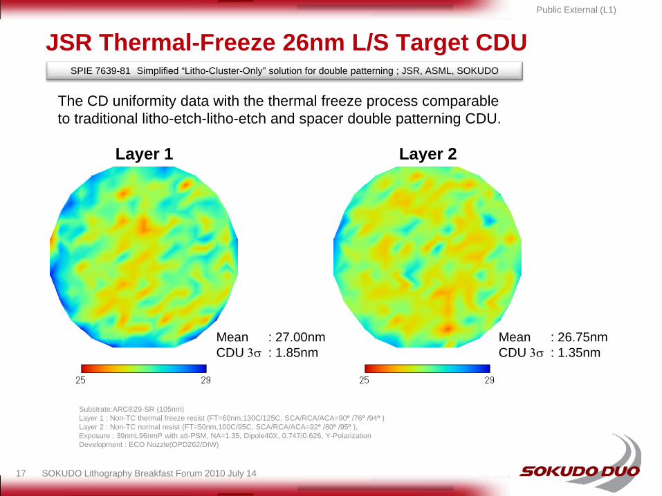
JSR Thermal-Freeze 26nm L/S Target CDU
The CD uniformity data with the thermal freeze process comparableto traditional litho-etch-litho-etch and spacer double patterning CDU.
Substrate:ARC®29-SR (105nm)Layer 1 : Non-TC thermal freeze resist (FT=60nm,130C/125C, SCA/RCA/ACA=90º /76º /94º )Layer 2 : Non-TC normal resist (FT=50nm,100C/95C, SCA/RCA/ACA=92º /80º /95º ), Exposure : 39nmL96nmP with att-PSM, NA=1.35, Dipole40X, 0.747/0.626, Y-PolarizationDevelopment : ECO Nozzle(OPD262/DIW)
Layer 1 Layer 2
Mean : 27.00nmCDU 3σ : 1.85nm
Mean : 26.75nmCDU 3σ : 1.35nm
SPIE 7639-81 Simplified “Litho-Cluster-Only” solution for double patterning ; JSR, ASML, SOKUDO

18 SOKUDO Lithography Breakfast Forum 2010 July 14
Public External (L1)
integration for ASML NXE:3100 (EUV)
SOKUDO EUVL Coat/Develop Track Configurations ~120wphCoat: Underlayer, ResistDevelop: TMAH / TBAH developers; various rinse approachesBake: Biased Hot Plate (QBH) for CDU control / tuning;
“Q” Quick set-temperature change bake between lots
20 SOKUDO Lithography Breakfast Forum 2010 July 14
Public External (L1)
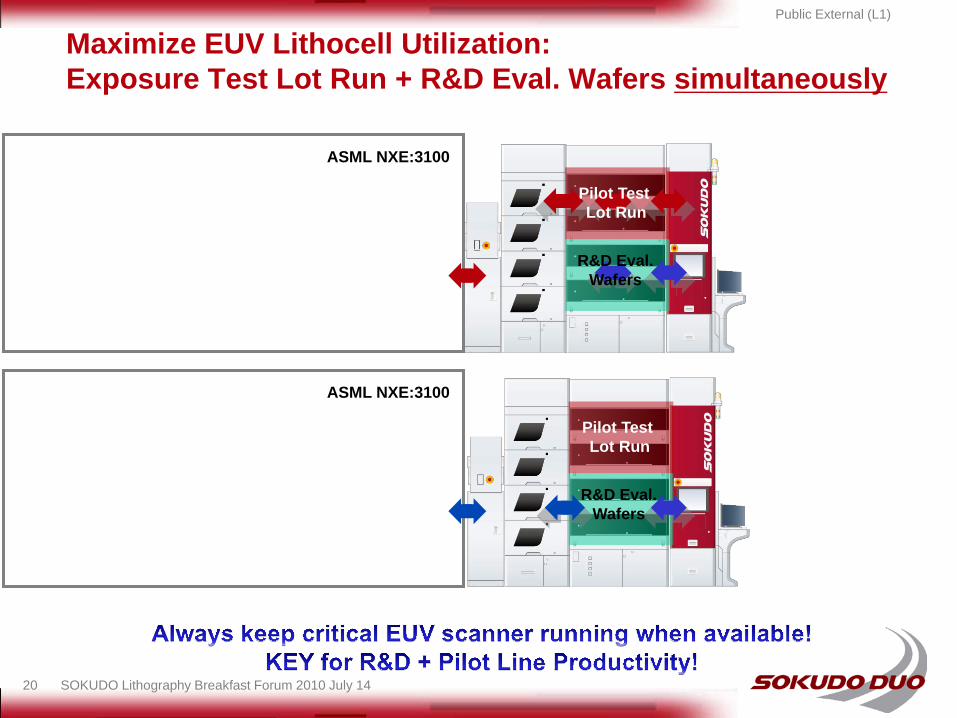
Maximize EUV Lithocell Utilization:Exposure Test Lot Run + R&D Eval. Wafers simultaneously
ASML NXE:3100
Pilot TestLot Run
ASML NXE:3100
R&D Eval.Wafers
R&D Eval.Wafers
Pilot TestLot Run
21 SOKUDO Lithography Breakfast Forum 2010 July 14
Public External (L1)
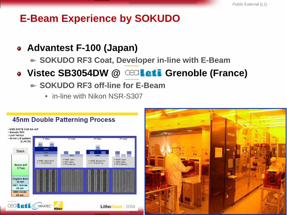
E-Beam Experience by SOKUDO
Advantest F-100 (Japan)SOKUDO RF3 Coat, Developer in-line with E-Beam
Vistec SB3054DW @ Grenoble (France)SOKUDO RF3 off-line for E-Beam
• in-line with Nikon NSR-S307

23 SOKUDO Lithography Breakfast Forum 2010 July 14
Public External (L1)
E-Beam Coat/Develop Track in-line with MAPPER
*
*
*
*
SOKUDO DUO Track
~100-120 WPH
*
MAPPER E-Beam Cluster
Target 100 WPH
2C = Underlayer2C = RESIST4D = DEVELOPwith Backside Scrub+ E-Beam interface
Sokudo Restricted DND (L4)

24 SOKUDO Lithography Breakfast Forum 2010 July 14
Public External (L1)
EUV, E-Beam Common Resist Process Development Focus Points
Reference: SPIE 7636-27, February 2010, San Jose, CA USA
Resist Manufacturers Continuously Reformulating for
Line Width Roughness (LWR)Sensitivity to DoseResolution 32 nm 22 nm
32 nm 22 nm CD LWR,Pattern Collapse & DefectivityTrack Process Studies:
Develop methods, solutionsRinse methods, solutions

25 SOKUDO Lithography Breakfast Forum 2010 July 14
Public External (L1)
SPIE Advanced Lithography 20097273-111 Development of EUV resists at Selete
SELETE (SOKUDO assignee, Koji Kaneyama)7273-115 EUV resist processing in vacuum
SELETE, SOKUDO
International Symposium on EUVL 2009Resist II EUV resist materials and processing at Selete
SELETE (SOKUDO assignee, Koji Kaneyama)Poster 94 Study of post-develop defect on typical EUV resist
SOKUDO
SPIE Advanced Lithography 20107636-111 Study of post-develop defect on typical EUV resist
SOKUDO 7636-115 Alternative resist processes for LWR reduction in EUVL
SELETE (SOKUDO assignee, Koji Kaneyama)7639-26 Development of EUV-resists based on various new materials
SELETE (SOKUDO assignee, Koji Kaneyama)7636-27 Development of resist material process for hp 2x nm devices using EUV lithography
SELETE (SOKUDO assignee, Koji Kaneyama)
SOKUDO EUVL Technical Papers History

26 SOKUDO Lithography Breakfast Forum 2010 July 14
Public External (L1)
Coat, Bake & Develop Track Process Knobs
DEVELOP Defect Control Approach
Wafer Rinse & Dry
Surfactant Rinse
Developer Chemistries:
TMAH, TBAH(?)
Negative Develop(?)
BAKE & CHILL Post-Expose (PEB) for
CD Uniformity control
High Temp. (PAB, BARC)
SPIN COAT Dispense Chemistries:
Underlayer +
Photo Resist
Thin-film coating recipe
40-60nm thickness
for EUV / E-Beam resist development

28 SOKUDO Lithography Breakfast Forum 2010 July 14
Public External (L1)
PEB in vacuum vs. atmosphere
28
Summary: Results
depend on resist,PEB in
Vacuummay be low value-added
BAKECustom built Vacuum PEB
“Baking Chamber” &“Cooling Chamber”
==<
>>>
MET-2D
SSR3
EUVResistType
EUVResistType
Reference: EUV resist processing in vacuum, Koji Kaneyama,Shinji Kobayashi, Toshiro Itani; Proc. SPIE 7273-115 (2009)

29 SOKUDO Lithography Breakfast Forum 2010 July 14
Public External (L1)
29
TBAH Developer extends CD capability,reduces pattern collapse
Reference: EUV resist materials and processing at Selete, K. Matsunaga, et.al.,International Symposium on EUV Lithography, October 2009, Prague
DEVELOP
30 SOKUDO Lithography Breakfast Forum 2010 July 14
Public External (L1)
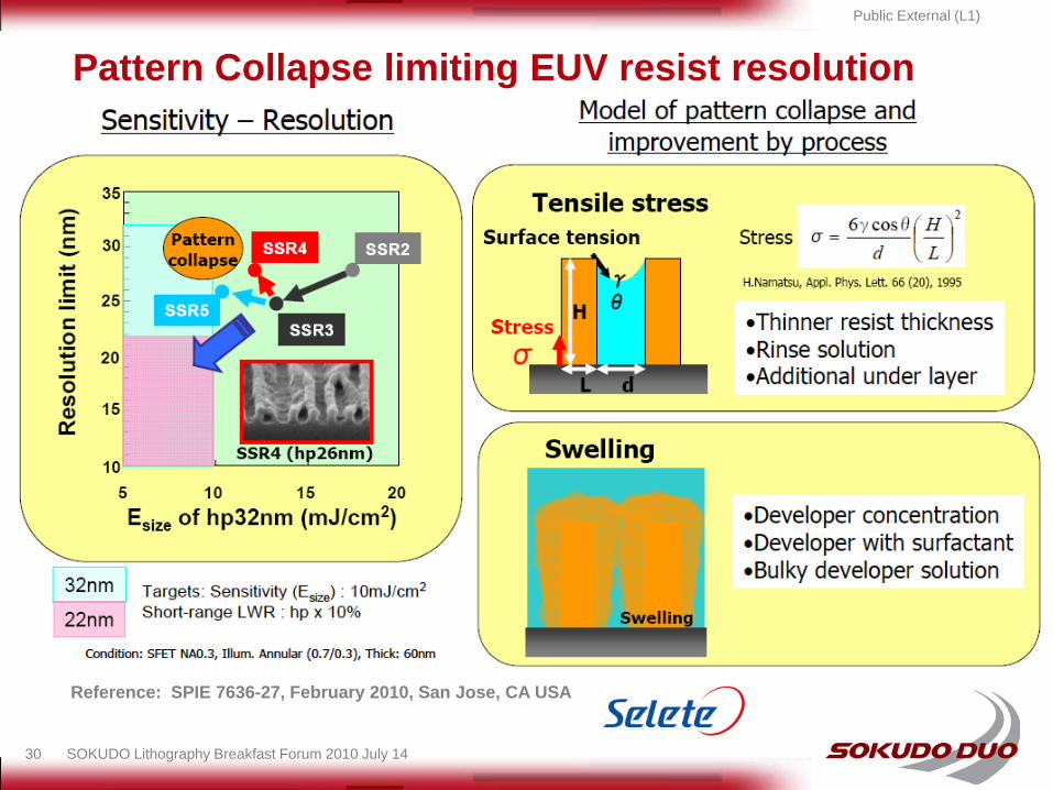
Pattern Collapse limiting EUV resist resolution
Reference: SPIE 7636-27, February 2010, San Jose, CA USA
31 SOKUDO Lithography Breakfast Forum 2010 July 14
Public External (L1)
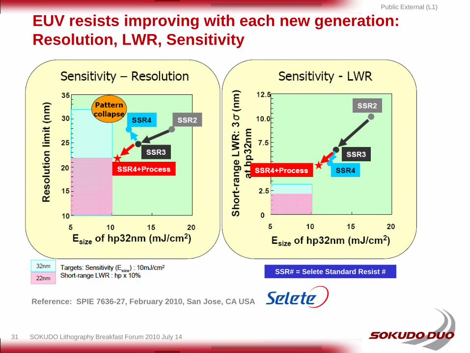
EUV resists improving with each new generation: Resolution, LWR, Sensitivity
Reference: SPIE 7636-27, February 2010, San Jose, CA USA
SSR# = Selete Standard Resist #

32 SOKUDO Lithography Breakfast Forum 2010 July 14
Public External (L1)
Common / specific defect history; EUV study started
MUV KrF ArF
λ=248nm λ=193nmλ≧365nm
ArFimmersion
Blo
bR
esid
ueEUV
λ=13.5nm
micro-Bubble Bottom-ARC µ-BridgeWater Droplet
before PEB
None
Com
mon
D
efec
tsSp
ecifi
c D
efec
t
33 SOKUDO Lithography Breakfast Forum 2010 July 14
Public External (L1)
EUV & E-Beam …
Although EUV may be leading the march towards 22 nm, E-Beam can close gap with (MAPPER) throughput plans for improvement towards 2012+
SOKUDO participating in EUV and E-Beam collaborations
EUVL consortia resist evaluations and characterization
E-Beam IMAGINE project resist process qualification
EUV and E-Beam resists following similar trends and challenges:In parallel transitioning from 32nm 22 nm process developmentBoth resist systems largely based on reformulating i/KrF generation blendsResist trending to thinner coatings: 40-60 nm target thicknessResolution – LWR – Sensitivity (RLS) all common issues

SOKUDO Lithography Breakfast Forum 2010 July 14 (L1)
“Shooting for the 22nm Lithography Goal” with the
Coat/Develop Track