service manual adjustable frequency ac...
TRANSCRIPT

Service Manual1336 FORCEAdjustableFrequency AC DriveBP300 – BP450
Allen-Bradley

Because of the variety of uses for the products described in thispublication, those responsible for the application and use of thiscontrol equipment must satisfy themselves that all necessarysteps have been taken to assure that each application and usemeets all performance and safety requirements, including anyapplicable laws, regulations, codes and standards.
The illustrations, charts, sample programs and layout examplesshown in this guide are intended solely for purposes of example.Since there are many variables and requirements associated withany particular installation, Rockwell Automation does notassume responsibility or liability (to include intellectual propertyliability) for actual use based upon the examples shown in thispublication.
Rockwell Automation publication SGI-1.1, Safety Guidelines forthe Application, Installation, and Maintenance of Solid-StateControl (available from your local Rockwell Automation office),describes some important differences between solid-stateequipment and electromechanical devices that should be takeninto consideration when applying products such as thosedescribed in this publication.
Reproduction of the contents of this copyrighted publication, inwhole or in part, without written permission of RockwellAutomation, is prohibited.
Throughout this manual we use notes to make you aware ofsafety considerations:
!ATTENTION: Identifies information aboutpractices or circumstances that can lead to personalinjury or death, property damage or economic loss.
Attention statements help you to:
• identify a hazard
• avoid the hazard
• recognize the consequences
Important: Identifies information that is critical for successfulapplication and understanding of the product.
ControlNet is a trademark; PLC is a registered trademark of Rockwell Automation.
Important User Information

Summary of Changes
Publication 1336 FORCE-6.16 – August, 1999
Summary of Changes
The information below summarizes the changes to thecompany-wide templates since the last release.
The derating tables in the Preface have been removed. Refer to the1336 FORCE User Manual.
Updated Information

Summary of Changes
Publication 1336 FORCE-6.16 – August, 1999
This Page Intentionally Left Blank

Publication 1336 FORCE-6.16 – August, 1999
Manual Objective P–1. . . . . . . . . . . . . . . . . . . . . . . . . . . . . . . . . . . . . Who Should Use This Manual P–1. . . . . . . . . . . . . . . . . . . . . . . . . . . . Safety Precautions P–1. . . . . . . . . . . . . . . . . . . . . . . . . . . . . . . . . . . . Electrostatic Discharge Precautions P–2. . . . . . . . . . . . . . . . . . . . . . . 1336 FORCE Product Identification P–3. . . . . . . . . . . . . . . . . . . . . . . .
Drive Nameplate Location P–3. . . . . . . . . . . . . . . . . . . . . . . . . . . . Software Compatibility P–3. . . . . . . . . . . . . . . . . . . . . . . . . . . . . . .
Drive and Option Identification P–4. . . . . . . . . . . . . . . . . . . . . . . . . . . 1336 FORCE Drive Catalog Numbers P–4. . . . . . . . . . . . . . . . . . . . Adapter Options – Factory Installed (Select One) P–4. . . . . . . . . . . . Drive Rating Qualifications P–5. . . . . . . . . . . . . . . . . . . . . . . . . . . . Enclosure Type P–5. . . . . . . . . . . . . . . . . . . . . . . . . . . . . . . . . . . .
Conventions P–6. . . . . . . . . . . . . . . . . . . . . . . . . . . . . . . . . . . . . . . . Auxiliary Input P–6. . . . . . . . . . . . . . . . . . . . . . . . . . . . . . . . . . . . . Auxiliary Interlock P–6. . . . . . . . . . . . . . . . . . . . . . . . . . . . . . . . . . Bit P–6. . . . . . . . . . . . . . . . . . . . . . . . . . . . . . . . . . . . . . . . . . . . . Check P–6. . . . . . . . . . . . . . . . . . . . . . . . . . . . . . . . . . . . . . . . . . . Connector P–6. . . . . . . . . . . . . . . . . . . . . . . . . . . . . . . . . . . . . . . . Control Interface L-Option Board P–7. . . . . . . . . . . . . . . . . . . . . . . . Default P–7. . . . . . . . . . . . . . . . . . . . . . . . . . . . . . . . . . . . . . . . . . Enable Input P–7. . . . . . . . . . . . . . . . . . . . . . . . . . . . . . . . . . . . . . False P–7. . . . . . . . . . . . . . . . . . . . . . . . . . . . . . . . . . . . . . . . . . . Jumper P–7. . . . . . . . . . . . . . . . . . . . . . . . . . . . . . . . . . . . . . . . . . Parameter P–7. . . . . . . . . . . . . . . . . . . . . . . . . . . . . . . . . . . . . . . . Press P–7. . . . . . . . . . . . . . . . . . . . . . . . . . . . . . . . . . . . . . . . . . . True P–8. . . . . . . . . . . . . . . . . . . . . . . . . . . . . . . . . . . . . . . . . . . .
Related Publications P–8. . . . . . . . . . . . . . . . . . . . . . . . . . . . . . . . . .
Chapter 1
Chapter Objectives 1–1. . . . . . . . . . . . . . . . . . . . . . . . . . . . . . . . . . . Chapter Overview 1–1. . . . . . . . . . . . . . . . . . . . . . . . . . . . . . . . . . . . Control Interface Option 1–3. . . . . . . . . . . . . . . . . . . . . . . . . . . . . . . .
Control Interface Board Jumpers 1–4. . . . . . . . . . . . . . . . . . . . . . . . Available Inputs 1–5. . . . . . . . . . . . . . . . . . . . . . . . . . . . . . . . . . . .
Local Programming 1–5. . . . . . . . . . . . . . . . . . . . . . . . . . . . . . . . . . . Adapters and Communication Ports 1–11. . . . . . . . . . . . . . . . . . . . . . .
Human Interface Module 1–11. . . . . . . . . . . . . . . . . . . . . . . . . . . . . Standard Adapter Ports 1–12. . . . . . . . . . . . . . . . . . . . . . . . . . . . . . PLC Comm Adapter Ports 1–12. . . . . . . . . . . . . . . . . . . . . . . . . . . . HIM Removal 1–13. . . . . . . . . . . . . . . . . . . . . . . . . . . . . . . . . . . . . HIM Operation 1–14. . . . . . . . . . . . . . . . . . . . . . . . . . . . . . . . . . . . .
Table of Contents
Preface
Control Logic Wiring andAdapters

Table of Contentsii
Publication 1336 FORCE-6.16 – August, 1999
Graphic Programming Terminal 1–15. . . . . . . . . . . . . . . . . . . . . . . . . . . GPT Description 1–15. . . . . . . . . . . . . . . . . . . . . . . . . . . . . . . . . . .
Drive Tools 1–16. . . . . . . . . . . . . . . . . . . . . . . . . . . . . . . . . . . . . . . . . Control Firmware Function 1–16. . . . . . . . . . . . . . . . . . . . . . . . . . . . . .
Chapter 2
Chapter Objectives 2–1. . . . . . . . . . . . . . . . . . . . . . . . . . . . . . . . . . . Disassembly and Access Overview 2–1. . . . . . . . . . . . . . . . . . . . . . . . Electrostatic Discharge Precautions 2–1. . . . . . . . . . . . . . . . . . . . . . .
Tools 2–2. . . . . . . . . . . . . . . . . . . . . . . . . . . . . . . . . . . . . . . . . . . Fastener Torque Specifications 2–2. . . . . . . . . . . . . . . . . . . . . . . . . . .
Torque Sequence 2–2. . . . . . . . . . . . . . . . . . . . . . . . . . . . . . . . . . Torque Specifications 2–3. . . . . . . . . . . . . . . . . . . . . . . . . . . . . . . .
Disassembly and Access Procedures 2–5. . . . . . . . . . . . . . . . . . . . . . Removing the High Voltage Guard 2–5. . . . . . . . . . . . . . . . . . . . . .
Removal 2–6. . . . . . . . . . . . . . . . . . . . . . . . . . . . . . . . . . . . . . . Installation 2–6. . . . . . . . . . . . . . . . . . . . . . . . . . . . . . . . . . . . . .
Removing Control Interface L-Option Board MOD-L4, -L5, or -L6 2–7. Removal 2–7. . . . . . . . . . . . . . . . . . . . . . . . . . . . . . . . . . . . . . . Installation 2–8. . . . . . . . . . . . . . . . . . . . . . . . . . . . . . . . . . . . . .
Removing the Circuit Board Platform 2–9. . . . . . . . . . . . . . . . . . . . . Removal 2–9. . . . . . . . . . . . . . . . . . . . . . . . . . . . . . . . . . . . . . . Installation 2–11. . . . . . . . . . . . . . . . . . . . . . . . . . . . . . . . . . . . . .
Removing the Main Control Board 2–12. . . . . . . . . . . . . . . . . . . . . . . Removal 2–13. . . . . . . . . . . . . . . . . . . . . . . . . . . . . . . . . . . . . . . Installation 2–14. . . . . . . . . . . . . . . . . . . . . . . . . . . . . . . . . . . . . .
Removing the Standard Adapter Board 2–15. . . . . . . . . . . . . . . . . . . Removal 2–15. . . . . . . . . . . . . . . . . . . . . . . . . . . . . . . . . . . . . . . Installation 2–16. . . . . . . . . . . . . . . . . . . . . . . . . . . . . . . . . . . . . .
Removing the PLC Comm Adapter Board 2–17. . . . . . . . . . . . . . . . . Removal 2–17. . . . . . . . . . . . . . . . . . . . . . . . . . . . . . . . . . . . . . . Installation 2–18. . . . . . . . . . . . . . . . . . . . . . . . . . . . . . . . . . . . . .
Removing the Control Board/Adapter Mounting Plate 2–19. . . . . . . . . Removal 2–19. . . . . . . . . . . . . . . . . . . . . . . . . . . . . . . . . . . . . . . Installation 2–20. . . . . . . . . . . . . . . . . . . . . . . . . . . . . . . . . . . . . .
Removing the Gate Driver Board from the Mounting Plate 2–21. . . . . . Removal 2–21. . . . . . . . . . . . . . . . . . . . . . . . . . . . . . . . . . . . . . . Installation 2–23. . . . . . . . . . . . . . . . . . . . . . . . . . . . . . . . . . . . . .
Removing the Precharge Board from the Mounting Plate 2–24. . . . . . . Removal 2–24. . . . . . . . . . . . . . . . . . . . . . . . . . . . . . . . . . . . . . . Installation 2–25. . . . . . . . . . . . . . . . . . . . . . . . . . . . . . . . . . . . . .
Removing a Power Module Snubber Board 2–26. . . . . . . . . . . . . . . . Removal 2–26. . . . . . . . . . . . . . . . . . . . . . . . . . . . . . . . . . . . . . . Installation 2–28. . . . . . . . . . . . . . . . . . . . . . . . . . . . . . . . . . . . . .
Disassembly and AccessProceduresDisassembly and AccessProcedures

Table of Contents iii
Publication 1336 FORCE-6.16 – August, 1999
Removing an Input Rectifier Snubber Board 2–29. . . . . . . . . . . . . . . . Removal 2–29. . . . . . . . . . . . . . . . . . . . . . . . . . . . . . . . . . . . . . . Installation 2–30. . . . . . . . . . . . . . . . . . . . . . . . . . . . . . . . . . . . . .
Accessing Power Plane Components 2–30. . . . . . . . . . . . . . . . . . . .
Chapter 3
Chapter Objectives 3–1. . . . . . . . . . . . . . . . . . . . . . . . . . . . . . . . . . . Component Test Overview 3–1. . . . . . . . . . . . . . . . . . . . . . . . . . . . . . Electrostatic Discharge Precautions 3–2. . . . . . . . . . . . . . . . . . . . . . .
Tools 3–2. . . . . . . . . . . . . . . . . . . . . . . . . . . . . . . . . . . . . . . . . . . Test 1 – Testing the Gate Driver Board 3–3. . . . . . . . . . . . . . . . . . . . . . Test 2 – Testing the Precharge Board 3–6. . . . . . . . . . . . . . . . . . . . . . Test 3 – Testing the Power Modules 3–8. . . . . . . . . . . . . . . . . . . . . . . Test 4 – Testing the Bus Capacitors 3–12. . . . . . . . . . . . . . . . . . . . . . . . Test 5 – Testing the Input Rectifiers 3–15. . . . . . . . . . . . . . . . . . . . . . . .
Chapter 4
Chapter Objective 4–1. . . . . . . . . . . . . . . . . . . . . . . . . . . . . . . . . . . . Safety Precautions 4–1. . . . . . . . . . . . . . . . . . . . . . . . . . . . . . . . . . . . Electrostatic Discharge Precautions 4–1. . . . . . . . . . . . . . . . . . . . . . .
Tools 4–2. . . . . . . . . . . . . . . . . . . . . . . . . . . . . . . . . . . . . . . . . . . Major Component Replacement 4–2. . . . . . . . . . . . . . . . . . . . . . . . . . Detailed Product Identification 4–3. . . . . . . . . . . . . . . . . . . . . . . . . . . .
Bus Capacitor Bank 4–4. . . . . . . . . . . . . . . . . . . . . . . . . . . . . . . . . Removal 4–5. . . . . . . . . . . . . . . . . . . . . . . . . . . . . . . . . . . . . . . Installation 4–7. . . . . . . . . . . . . . . . . . . . . . . . . . . . . . . . . . . . . .
Thermistor 4–8. . . . . . . . . . . . . . . . . . . . . . . . . . . . . . . . . . . . . . . Removal 4–8. . . . . . . . . . . . . . . . . . . . . . . . . . . . . . . . . . . . . . . Installation 4–9. . . . . . . . . . . . . . . . . . . . . . . . . . . . . . . . . . . . . .
Power Modules 4–10. . . . . . . . . . . . . . . . . . . . . . . . . . . . . . . . . . . . Removal 4–10. . . . . . . . . . . . . . . . . . . . . . . . . . . . . . . . . . . . . . . Installation 4–12. . . . . . . . . . . . . . . . . . . . . . . . . . . . . . . . . . . . . .
Bus Fuses F1 4–13. . . . . . . . . . . . . . . . . . . . . . . . . . . . . . . . . . . . . Removal 4–13. . . . . . . . . . . . . . . . . . . . . . . . . . . . . . . . . . . . . . . Installation 4–14. . . . . . . . . . . . . . . . . . . . . . . . . . . . . . . . . . . . . .
Input Fuses 4–15. . . . . . . . . . . . . . . . . . . . . . . . . . . . . . . . . . . . . . . Removal 4–15. . . . . . . . . . . . . . . . . . . . . . . . . . . . . . . . . . . . . . . Installation 4–16. . . . . . . . . . . . . . . . . . . . . . . . . . . . . . . . . . . . . .
Ground Fault CT 4–17. . . . . . . . . . . . . . . . . . . . . . . . . . . . . . . . . . . Removal 4–17. . . . . . . . . . . . . . . . . . . . . . . . . . . . . . . . . . . . . . . Installation 4–19. . . . . . . . . . . . . . . . . . . . . . . . . . . . . . . . . . . . . .
Input Rectifiers 4–20. . . . . . . . . . . . . . . . . . . . . . . . . . . . . . . . . . . . Removal 4–20. . . . . . . . . . . . . . . . . . . . . . . . . . . . . . . . . . . . . . . Installation 4–22. . . . . . . . . . . . . . . . . . . . . . . . . . . . . . . . . . . . . .
Component Test Procedures
Part ReplacementProcedures

Table of Contentsiv
Publication 1336 FORCE-6.16 – August, 1999
LEMs 4–23. . . . . . . . . . . . . . . . . . . . . . . . . . . . . . . . . . . . . . . . . . . Removal 4–23. . . . . . . . . . . . . . . . . . . . . . . . . . . . . . . . . . . . . . . Installation 4–25. . . . . . . . . . . . . . . . . . . . . . . . . . . . . . . . . . . . . .
MOV Surge Suppressor 4–26. . . . . . . . . . . . . . . . . . . . . . . . . . . . . . Removal 4–26. . . . . . . . . . . . . . . . . . . . . . . . . . . . . . . . . . . . . . . Installation 4–27. . . . . . . . . . . . . . . . . . . . . . . . . . . . . . . . . . . . . .
Fan and Transformer Assembly 4–28. . . . . . . . . . . . . . . . . . . . . . . . Removal 4–28. . . . . . . . . . . . . . . . . . . . . . . . . . . . . . . . . . . . . . . Installation 4–30. . . . . . . . . . . . . . . . . . . . . . . . . . . . . . . . . . . . . .
DC Bus Inductor L1 4–32. . . . . . . . . . . . . . . . . . . . . . . . . . . . . . . . . Removal 4–32. . . . . . . . . . . . . . . . . . . . . . . . . . . . . . . . . . . . . . . Installation 4–34. . . . . . . . . . . . . . . . . . . . . . . . . . . . . . . . . . . . . .
Chapter 5
Chapter Objectives 5–1. . . . . . . . . . . . . . . . . . . . . . . . . . . . . . . . . . . Ordering Replacement Parts 5–1. . . . . . . . . . . . . . . . . . . . . . . . . . . . . Replacement Parts Listing 5–2. . . . . . . . . . . . . . . . . . . . . . . . . . . . . .
Chapter 6
Replacement Parts List
Schematics — 250 – 450 HP1336 FORCE Drives
Index

Preface
Publication 1336 FORCE-6.16 – August, 1999
Preface
The information in this manual is designed to help repair a RockwellAutomation Bulletin 1336 FORCE Adjustable Frequency AC Drivewith ratings BP300 – BP450.
This manual is intended for qualified service personnel responsiblefor repairing the 1336 FORCE Adjustable Frequency AC Drive. Youshould:
• Read this entire manual before performing maintenance or repairsto drives.
• Have previous experience with, and basic understanding of,electrical terminology, procedures, required troubleshootingequipment, equipment protection procedures and methods, andsafety precautions.
This manual describes equipment and disassembly procedures. Youbegin with general illustrations and end with greater detailconcerning replacement parts and part locations on the drives. Laterchapters may refer you back to earlier chapters for information onbasic equipment and steps necessary to perform detailed diagnosticsand part replacement.
!ATTENTION: Some printed circuit boards and drivecomponents may contain hazardous voltage levels.Remove and lock out power before you disconnect orreconnect wires, and before you remove or replacefuses and circuit boards. Verify bus voltage bymeasuring the voltage between the +DC/–DC BrakeTerminals. Do not attempt to service the drive until thebus voltage has discharged to zero volts.
Manual Objective
Who Should Use ThisManual
Safety Precautions

PrefaceP–2
Publication 1336 FORCE-6.16 – August, 1999
!ATTENTION: Potentially fatal voltages may resultfrom improper usage of oscilloscope and other test equip-ment. The oscilloscope chassis may be at a potentially fa-tal voltage if not properly grounded. If an oscilloscope isused to measure high voltage waveforms, use only a dualchannel oscilloscope in the differential mode with X 100probes. It is recommended that the oscilloscope be usedin the A minus B Quasi-differential mode with the oscillo-scope chassis correctly grounded to an earth ground.
!ATTENTION: Only personnel familiar with the1336 FORCE Adjustable Frequency AC Drive andassociated machinery should plan or implement theinstallation, start-up and subsequent maintenance of thesystem. Failure to comply may result in personal injuryand/or equipment damage.
!ATTENTION: This assembly contains parts andsub-assemblies that are sensitive to electrostaticdischarge. Static control precautions are required whenservicing this assembly. Component damage may resultif you ignore electrostatic discharge control procedures.If you are not familiar with static control procedures,reference Rockwell Automation Publication8000-4.5.2, Guarding Against Electrostatic Damage, orany other applicable ESD protection handbook.
Electrostatic discharge generated by static electricity can damage thecomplimentary metallic oxide semiconductor devices on variousdrive boards. It is recommended that you perform these proceduresto guard against this type of damage when circuit boards areremoved or installed:
• Wear a wrist-type grounding strap that is grounded to the drivechassis.
• Attach the wrist strap before removing the new circuit board fromthe conductive packet.
• Remove boards from the drive and immediately insert them intotheir conductive packets.
Electrostatic DischargePrecautions
Preface P–3
Publication 1336 FORCE-6.16 – August, 1999
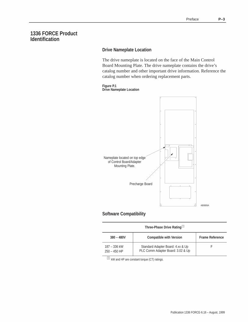
Drive Nameplate Location
The drive nameplate is located on the face of the Main ControlBoard Mounting Plate. The drive nameplate contains the drive’scatalog number and other important drive information. Reference thecatalog number when ordering replacement parts.
Figure P.1 Drive Nameplate Location
AB0806A
Nameplate located on top edgeof Control Board/Adapter
Mounting Plate.
Precharge Board
Software Compatibility
Three-Phase Drive Rating �
380 – 480V Compatible with Version Frame Reference
187 – 336 kW250 – 450 HP
Standard Adapter Board: 4.xx & UpPLC Comm Adapter Board: 3.02 & Up
F
� kW and HP are constant torque (CT) ratings.
1336 FORCE ProductIdentification

PrefaceP–4
Publication 1336 FORCE-6.16 – August, 1999
The following is an explanation of the catalog numbering system for1336 FORCE Adjustable Frequency AC Drives and options. Thecatalog number is coded to identify the drive power rating and can befound on the drive shipping carton and nameplate.
1336 FORCE Drive Catalog Numbers
Table P.A
1336T – B007 – AA – GT2EN – L6
BULLETIN NO. DRIVE RATING(MUST BE SPECIFIED)
ENCLOSURE STYLE(MUST BE SPECIFIED)
ADAPTER�
(MUST BE SPECIFIED)OPTIONS
(AS REQUIRED)
Adapter Options – Factory Installed (Select One)�
Description � Option Code
PLC Communication Adapter English – GT1EN
Standard Adapter English – GT2EN
No Adapter – GTO�
380 – 480V AC Input, Constant Drive
Enclosures
Drive Rating � OpenIP00
No Enclosure
NEMA Type 1IP20
General Purpose
NEMA Type 4IP65
Resist Water, Dust
NEMA Type 12IP54
Industrial Use
FrameConstant Torque
FrameDesignation Output
AmpsNominal HP Code Code Code Code
F 406.4 300 BP300-AN� BP300-AA� � �
459.2 350 BP350-AN� BP350-AA� � �
481.0 400 BP400-AN� BP400-AA� � �
531.7 450 BP450-AN� BP450-AA� � �
� Drive rating is based on a carrier frequency of 4kHz maximum, an altitude of 1,000 meters or less, and a maximumambient temperature of 40°C.
� Refer to the Language Module and Options tables following these Catalog Number tables.� Not available in this rating.� An adapter Board (see Adapter Options – Factory Installed table) is required to make the drive functional. If the
“–GTO option” (no adapter) is chosen, then the Adapter Kit must be added after shipment.� A “Common Mode Choke” option (–CM) or “No Common Mode Choke” option (–NCM) must be specified with each
F-Frame Drive.
Drive and OptionIdentification

Preface P–5
Publication 1336 FORCE-6.16 – August, 1999
Table P.B
OptionsCode� Description � Code Description �
Human Interface Module, NEMA Type 1 (IP 20) Communication Options
HABHAPHA1HA2
Blank – No FunctionalityProgrammer OnlyProgrammer/Controller w/Analog PotProgrammer/Controller w/Digital Pot
GM1GM2GM3
Single Point Remote I/ORS-232/422/485, DF1 & DH485DeviceNet
Human Interface Module, NEMA Type 12 (IP 54) Control Interface Options
HJPHJ2
Programmer OnlyProgrammer/Controller w/Digital Pot
L4L4EL5
TTL ContactTTL Contact & Encoder Feedback24V AC/DCL5
L5EL6
24V AC/DC24V AC/DC & Encoder Feedback115V ACL6
L6E115V AC115V AC & Encoder Feedback
� Must be used in conjunction with a standard adapter option –GT2EN� For a more functionally complete description of each option refer to Publication 1336 FORCE-1.0.
Drive Rating Qualifications
Several factors can affect drive rating. If more than one factor exists,derating percentages must be multiplied. For example, if a 14-ampdrive is installed at a 2km (6,600 ft.) altitude and has a 2%high-input line voltage, the actual amp rating is:14 x 94% altitudederating x 96% high-input line derating = 12.6 amps
Enclosure Type
The first character, A, indicates the Enclosure Code.
The second character indicates the type of enclosure shipped fromthe factory:
Table P.C Enclosure Type Code Description
Enclosure Type Code Description
N Open style (IP 00)
A NEMA Type 1 (IP 20)
F NEMA Type 4 (IP 65)
J NEMA Type 12 (IP 54)

PrefaceP–6
Publication 1336 FORCE-6.16 – August, 1999
To help differentiate parameter names and display text from othertext in this manual, the following conventions will be used:
• Parameter Names will appear in [brackets].
• Display Text will appear in “quotes”.
The following is a list of conventions used throughout this manual,and definitions of the conventions. For a list of terminology anddefinitions, refer to the Glossary in the back of this manual.
Auxiliary Input
The Auxiliary Input is a terminal connection on the Control InterfaceL-Option Board. This connection provides an external input for useas an Auxiliary Interlock. Unless this interlock is closed, the drivewill be faulted with an Auxiliary Fault.
Auxiliary Interlock
The Auxiliary Interlock is a user-supplied circuit consisting of reset,overload, or other interlocking circuitry. The Interlock is wired to thedrive Auxiliary input.
Bit
A bit is a single character or status point used in programmablelogic. Eight bits form a BYTE, 16 bits form a word. Driveparameters are actually eight bits or 16 bit words.
Check
To check means to examine either the physical condition ofsomething or the setting of some control, such as a Parameter.Checking a drive board or component may also requiremeasurements and tests.
Connector
A connector connects one drive board to another. Connectors comein two designs, male and female. Male connectors are stationary andcontain pins, which are sometimes joined by jumpers. Femaleconnectors are at the ends of wires or ribbon cables and plug intomale connectors.
Conventions

Preface P–7
Publication 1336 FORCE-6.16 – August, 1999
Control Interface L-Option Board
A Control Interface L-Option Board plugs into connectors J7 and J9,located on the lower portion of the Main Control Board. This boardis identified as L4/4E, L5/5E or L6/6E and provides optional controlwiring configurations for a drive.
Default
When a drive function defaults, it automatically changes to apre-programmed setting.
Enable Input
The Enable Input is a terminal connection on the Control InterfaceL-Option Board. This connection provides an external input toenable or disable the Drive Output section. It must be true to permitthe drive to operate.
False
False refers to a logical false state. For instance, a Control Interfacesignal on TB3 is false when the input contact is open or theappropriate voltage is not applied to the Control Interface L-OptionBoard.
Jumper
A jumper completes a circuit between two pins within a maleconnector on a drive board. In the absence of certain optionalequipment using female connectors, jumpers are applied to certainpins within a male connector to complete specific and necessarycircuits.
Parameter
Parameters are programmable drive functions that define variousoperating functions or status displays of a drive. Refer to Bulletin1336 FORCE Adjustable Frequency AC Drive User Manual forParameter details.
Press
Press a button on the Human Interface Module to change Parametersettings and drive functions.

PrefaceP–8
Publication 1336 FORCE-6.16 – August, 1999
True
True refers to a logical true state. For instance, a Control Interfacesignal on TB3 is true when: L4/L4E contact input is closed, L5/L5Einput terminal registers 24V, or L6/L6E input terminal registers115V AC.
The following lists other Rockwell Automation publications thatapply to the 1336 FORCE Adjustable Frequency AC Drives:
• Product Data Drive Tools Software (9303-2.0)
• Bulletin 1201 Graphic Programming Terminal User Manual(1201-5.0)
• Product Pricing Bulletin (1336 FORCE-3.0)
• 1336 FORCE Field Oriented Control User Manual (1336FORCE-5.12)
• 1336 FORCE PLC Communications Adapter User Manual (1336FORCE-5.13)
• Renewal Parts List (1336 FORCE-6.0)
• Options Manuals/Instructions
Related Publications

Chapter 1
Publication 1336 FORCE-6.16 – August, 1999
Control Logic Wiring and Adapters
This chapter introduces you to terminal block locations and wiringand to adapter locations and functions.
This chapter illustrates and describes the Standard Adapter Board:
• Control Logic Interface Options L4, L5, and L6, includingterminal block TB3
• TB3 input mode selections and functions
• TB3, TB5, TB6, TB7 terminal designations
This chapter illustrates and describes the following terminaldesignations for the PLC Comm Adapter Board:
• TB20
• TB21
Important: All printed circuit boards, except the Main ControlBoard assembly, are referenced to negative ground(–bus).
!ATTENTION : Some printed circuit boards and drivecomponents may contain hazardous voltage levels.Remove power before you disconnect or reconnectwires, and before you remove or replace fuses andcircuit boards. Verify bus voltage by measuring thevoltage between the +DC/–DC Brake Terminals. Donot attempt to service the drive until the bus voltagehas discharged to zero volts.
!ATTENTION: This assembly contains parts andsub-assemblies that are sensitive to electrostaticdischarge. Static control precautions are required whenservicing this assembly. Component damage may resultif you ignore electrostatic discharge control procedures.If you are not familiar with static control procedures,reference Rockwell Automation Publication8000-4.5.2, Guarding Against Electrostatic Discharge,or any other applicable ESD protection handbook.
Chapter Objectives
Chapter Overview

1–2 Control Logic Wiring and Adapters
Publication 1336 FORCE-6.16 – August, 1999
Figure 2.1 Standard Adapter Terminal Block Locations
TB1 PowerTerminal Block
AB0564A
JOG
ESC SEL
Main ControlBoard
StandardAdapter Board
TB10 Encoder
TB11
TB5, TB6, TB7Control and
Signal Wiring
TB3 ControlL-Option Board
Control InterfaceL-Option Board
TB6 TB7TB5Control and Signal Wiring
Figure 2.2 PLC Comm Adapter Terminal Block Locations
CommunicationChannels
TB1 PowerTerminal Block
AB0565C
Main ControlBoard
PLC CommBoard
TB10 Encoder
TB11
TB20, TB21Control and
Signal Wiring

1–3Control Logic Wiring and Adapters
Publication 1336 FORCE-6.16 – August, 1999
!ATTENTION: The National Electrical Code (NEC)and local codes outline provisions for safely installingelectrical equipment. Installation must comply withspecifications regarding wire types, conductor sizes,branch circuit protection and disconnect devices.Failure to do so may result in personal injury and/orequipment damage.
The Control Interface L-Option Board provides a means ofinterfacing various signals and commands to the 1336 FORCE byusing contact closures.
Six different versions of the option are available:
L4 Contact Closure Interface1
L4E Contact Closure Interface with Encoder Feedback Inputs1
L5 +24V AC/DC Interface
L5E +24V AC/DC Interface with Encoder Feedback Inputs
L6 115V AC Interface
L6E 115V AC Interface with Encoder Feedback Inputs
1 Uses internal +5V DC supply.
The user inputs are connected to the Control Interface L-OptionBoard through TB3. The L4, L5 and L6 options each have ninecontrol inputs. The function of each input must be selected throughprogramming as explained later in this section. The L4E, L5E andL6E options are similar to L4, L5 and L6 with the addition ofencoder feedback inputs.
Control Interface Option

1–4 Control Logic Wiring and Adapters
Publication 1336 FORCE-6.16 – August, 1999
Control Interface Board Jumpers
Important: If the Control Interface L-Option Board is beinginstalled, Standard Adapter Board jumpers at pins 3 & 4and 17 & 18 of J10 must be removed. If this board isremoved, these jumpers must be reinstalled and the[Input Mode] parameter must be programmed to “1”.
Figure 2.3 Jumper Locations
AB0819A
Jumper J10(Located on Standard
Adapter Board)

1–5Control Logic Wiring and Adapters
Publication 1336 FORCE-6.16 – August, 1999
Available Inputs
A variety of combinations made up of the following inputs areavailable.
Start Enable
Stop/Clear Fault Auxiliary
Reverse 2 Stop Mode Selects
Digital Potentiometer (MOP) Run Forward
2 Accel/Decel Rates Run Reverse
3 Speed Selects Local Control
The available combinations are shown in Figure 2.5. Programmingthe [Input Mode] parameter to one of the Input Mode numbers listedselects that combination of input functions.
Important: The [Input Mode] parameter can be changed at anytime; however, programming changes will not takeaffect until power has been cycled to the drive. Whenchanging an input mode, it is important to note that thecorresponding inputs to TB3 may also change.
The programming options of the Control Interface Option allow theuser to select an input combination to meet the needs of a specificinstallation. Appropriate selection of a combination may be done byusing Table 1.A. First determine the type of start/stop/directioncontrol desired. Then select the remaining control functionsavailable. After selecting a group of Input Modes use Table 1.A forspecific mode selection. Record the selected mode number below.
Selected Mode Number:
For local programming and control information, refer to the1336 FORCE User Manual.
Local Programming
1–6 Control Logic Wiring and Adapters
Publication 1336 FORCE-6.16 – August, 1999
Table 2.A Input Mode Selection
Start/Stop Type Direction Control Communication CompatibilityMode(s)to Use
Stop & EnableOnly
None Control must be provided by HIM or Communication Option. 1
MomentaryPushbutton(3 Wire)
Maintained Switch(Open-Forward,Closed-Reverse)
Start/Stop – works in parallel with HIM and Communication Options.Direction Control will not work in parallel with HIM or CommunicationOptions. User must select direction control from either HIM andCommunication Options or TB3 input.
2 – 6
MomentaryPushbutton(3 Wire)
Momentary Pushbuttons(Forward and Reverse)
Start/Stop – works in parallel with HIM and Communication Options.Direction – works in parallel with HIM or Communication Options. 7 – 11
Maintained switches for combined run and directioncontrol (2 wire, Run Forward, Run Reverse)
Start – works differently than three-wire control.�
Direction – works differently than three-wire control.�
Stop – always works.
12 – 16
� Refer to two-, three-wire notes in the user manual.
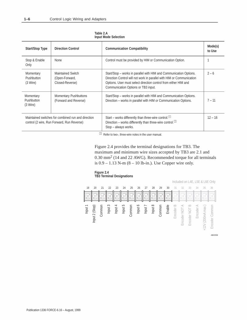
Figure 2.4 provides the terminal designations for TB3. Themaximum and minimum wire sizes accepted by TB3 are 2.1 and0.30 mm2 (14 and 22 AWG). Recommended torque for all terminalsis 0.9 – 1.13 N-m (8 – 10 lb-in.). Use Copper wire only.
Figure 2.4 TB3 Terminal Designations
19 20 21 22 23 24 25 26 27 28 29 30 31 32 33 34 35 36
Inpu
t 1
Inpu
t 2 (S
top)
Com
mon
Inpu
t 3
Inpu
t 4
Inpu
t 5
Com
mon
Inpu
t 6
Inpu
t 7
Inpu
t 8
Com
mon
Enab
le
Enco
der B
Enco
der N
OT
A
Enco
der N
OT
B
Enco
der A
+12V
(200
mA
max
.)
Enco
der C
omm
on
AB0293B
Included on L4E, L5E & L6E Only

1–7Control Logic Wiring and Adapters
Publication 1336 FORCE-6.16 – August, 1999
Figure 2.5 Input Mode Selection and Typical TB3 Connections
Jog
19
20
21
22
23
24
25
26
27
28
29
30
Status
Common
Status
Status
Status
Common
Status
Status
Status
Common
[Input Mode] 1Factory Default
19
20
21
22
23
24
25
26
27
28
29
30
Start
Common
Common
Common
StopType
1st/2ndAccel
DigitalPot Up
Speed Speed 1st/2ndDecel
DigitalPot Dn
Local
2 3 4 5 6Mode
[Input Mode] 2 – 6
1 See Table 1.B.
Control by all other adapters is disabled (except Stop). 2 Drive must be stopped to take Local Control.
These inputs must be present before drive will start. 3
User
Con
nect
ions
User
Con
nect
ions
AB0290B
Momentary
Maintained
AT
TE
NT
ION
:pr
oper
ly u
nles
s a
SC
AN
port
opt
ion
is c
onne
cted
to
the
driv
e. T
o as
sure
pro
per
JOG
fun
ctio
n, in
stal
l at
leas
t on
eof
the
fol
low
ing:
1201
-HA
P,
1201
-HA
1, 1
201-
HA
2, 1
336-
GM
1. A
pplie
sto
130
5 w
ith f
irmw
are
FR
N 2
.01
or e
arlie
r an
d 13
36
PLU
S w
ith L
angu
age
Mod
ule
1336
S-E
N f
irmw
are
FR
N1.
05 o
r ea
rlier
.The
JO
G f
unct
ion
will
not
ope
rate
Enable3
Enable3
Stop/Fault Reset3
Stop/Clear Fault3,7,8
Ext. Fault3,5,9
Speed Select 21
Speed Select 11
Select 31 Select 31 Control2
Note: If this mode is selected, the status of allinputs can be read at the [Input Status] parameter.However, only “Stop/Fault Reset” and “Enable” willhave control function.
Three-Wire Control with Single-Source Reversing
Rev/Fwd4,6 Rev/Fwd4,6 Rev/Fwd4,6
Bit 0 of [Direction Mask] must = 1. 4For Common Bus – Precharge EnableBit 12 of Para 59 Logic Options must = 0 for Reverse Direction Control.
5
Soft Fault Reset Only, Must Cycle Power to Drive to Clear Hard Fault; 6
Soft Fault Refer to Para 59 to Configure Start & Stop Type.
7
8
Rev/Fwd4,6
Jog
Hard Fault = See Troubleshooting Section.
Rev/Fwd4,6
Can be masked out. 9
ProcTrim
Ramp
Rev/Fwd4,6
Flux EnJog
Reset
Rev/Fwd4,6
17 18

1–8 Control Logic Wiring and Adapters
Publication 1336 FORCE-6.16 – August, 1999
See Table 2.B. 1 Drive must be stopped to take Local Control.Control by all other adapters is disabled (except Stop).
2
These inputs must be present before drive will start. 3 Bit 0 of [Direction Mask] must = 1 to allow operation. 4
Rev4,6
Momentary
Maintained
Common
Run Reverse
Common
Common
Local StopType
1st/2ndAccel
DigitalPot Up
Local
Speed Speed 1st/2ndDecel
DigitalPot Dn
StopType
12 13 14 15 16Mode
[Input Mode] 12 - 16Two-Wire Control, Single-Source Control
19
20
21
22
23
24
25
26
27
28
29
30
Common
Common
Common
DigitalPot Dn
2ndAccel
Jog Spd Spd DigitalPot Up
1stDecel
[Input Mode] 7 - 11Three-Wire Control with Multi-Source Reversing
DigitalPot Up
1stAccel
7 8 9 10 11
Mode
Spd Spd Spd DigitalPot Dn
2ndDecel
19
20
21
22
23
24
25
26
27
28
29
30
User
Con
nect
ions
User
Con
nect
ions
AB0291B
AT
TE
NT
ION
:pr
oper
ly u
nles
s a
SC
AN
port
opt
ion
is c
onne
cted
to
the
driv
e. T
o as
sure
pro
per
JOG
fun
ctio
n, in
stal
l at
leas
t on
eof
the
fol
low
ing:
1201
-HA
P,
1201
-HA
1, 1
201-
HA
2, 1
336-
GM
1. A
pplie
sto
130
5 w
ith f
irmw
are
FR
N 2
.01
or e
arlie
r an
d 13
36
PLU
S w
ith L
angu
age
Mod
ule
1336
S-E
N f
irmw
are
FR
N1.
05 o
r ea
rlier
.The
JO
G f
unct
ion
will
not
ope
rate Stop/Clear Fault7,8
Ext Fault3,5,9
Speed Select 11
Enable3
Stop/Clear Fault3,7,8
Speed Select 21
Speed Select 11
Enable3
Sel 21 Sel 21 Sel 21
Select 31 Select 31
Control2 Control2
Sel 31 Sel 31
Rev4,6 Rev4,6
4,6
Run Forward4,6
Start6
Fwd6 Fwd6Fwd6
Ext Fault3,5,9
For Common Bus – Precharge EnableBit 12 of Para 59 Logic Options must = 0 reverse direction control.
5
Soft Fault Reset Only, Must cycle power to drive to clear; 6
Refer to Para 59 to configure Start & Stop type.
7
8Hard Fault –– see Troubleshooting.
Can be masked out. 9
Spd/Tq3
Spd/Tq2
Spd/Tq1
ProcTrim
Spd/Tq3
Spd/Tq2
Spd/Tq1
FluxEn
21
Parameter 53 (Spd/Tq Mode Sel) becomes read only. 10
ProcTrim
FluxEn
ProcTrim
Jog
Reset Reset SpeedSel 3
RampDis
23 24 25 26
Rev
Fwd
RampDis
Reset
Spd/Tq3
Spd/Tq2
Spd/Tq1
SpdSel 2
1910 2010 2210

1–9Control Logic Wiring and Adapters
Publication 1336 FORCE-6.16 – August, 1999
The following table defines the input state of the Speed Select inputsfor a desired frequency source.
Table 2.B Speed Select Input State vs. Velocity Reference Source
Speed Select 3 Speed Select 2 Speed Select 1 Velocity Reference Source
TB3 Terminal 26 Terminal 27 Terminal 28 Interface Option (MOD L4, L5, L6)
O O O Ext Ref 1 Para 1011
O O X Preset Speed Ref 1 (P 119)
O X O Preset Speed Ref 2 (P120)
O X X Preset Speed Ref 3 (P 121)
X O O Preset Speed Ref 4 (P 122)
X O X Preset Speed Ref 5 (P 123)
X X O External Reference 2 (P 104)
X X X Last State
Equivalent truth table implemented in Parameter 52 Logic Command Word
Para 52 Bit 14 Bit 13 Bit 12 Velocity Reference Source Bits
O O X Ext Ref 1 (P 101)
O X O Preset Speed Ref 1 (P 119)
O X X Preset Speed Ref 2 (P120)
X O O Preset Speed Ref 3 (P 121)
X O X Preset Speed Ref 4 (P 122)
X X O Preset Speed Ref 5 (P 123)
X X X External Reference 2 (P 104)
O O O No Reference or Last State
O = Open — Input Removed
X = Closed — Input Present1 Unless otherwise configured, this will default to the HIM speed reference input.
Figure 2.6 PLC Comm Adapter Reference Signal Connections
AB0551A
1 2 3 4 5 6 7 8 9 10 11 12 13 14 15 16 17 18 19
AnalogOut 1
AnalogOut 2
AnalogOut 3
AnalogOut 4
AnalogIn1
AnalogIn2
AnalogIn3
AnalogIn4
+10 Comm–10
1 2 3 4 5 6 7 8 9 10
DriveEnable
Stop
MotorThermo
ExtFault
CommonFaultRelay
TB20 TB21

1–10 Control Logic Wiring and Adapters
Publication 1336 FORCE-6.16 – August, 1999
Table 2.C PLC Comm Adapter Reference Signal Connections
Terminal Block Terminal Number(s) Signal
TB20 1 Drive Enable (NO)
2 Motor Thermoguard (NC)
3 Normal Stop (NC)
4 External Fault (NC)
5
6 Input Common
7
8 Fault Output (NC)
9 Fault Output (COM)
10 Fault Output (NO)
TB21 1 OUT 1
2 COM 1
3 COM 2
4 OUT 2
5 OUT 3
6 COM 3
7 OUT 4
8 COM 4
9 IN 1+
10 IN 1–
11 IN 2+
12 IN 2–
13 IN 3+
14 IN 3–
15 IN 4+
16 IN 4–
17 +10V
18 COM
19 –10V
1–11Control Logic Wiring and Adapters
Publication 1336 FORCE-6.16 – August, 1999
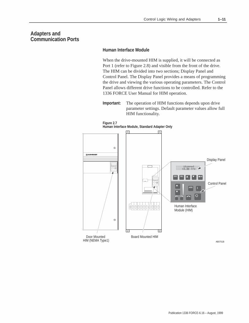
Human Interface Module
When the drive-mounted HIM is supplied, it will be connected asPort 1 (refer to Figure 2.8) and visible from the front of the drive.The HIM can be divided into two sections; Display Panel andControl Panel. The Display Panel provides a means of programmingthe drive and viewing the various operating parameters. The ControlPanel allows different drive functions to be controlled. Refer to the1336 FORCE User Manual for HIM operation.
Important: The operation of HIM functions depends upon driveparameter settings. Default parameter values allow fullHIM functionality.
Figure 2.7 Human Interface Module, Standard Adapter Only
Display Panel
Control Panel
Door Mounted HIM (NEMA Type1)
Board Mounted HIMAB0751B
Human InterfaceModule (HIM)
Adapters andCommunication Ports

1–12 Control Logic Wiring and Adapters
Publication 1336 FORCE-6.16 – August, 1999
Standard Adapter Ports
Figure 2.8 Standard Adapter Board Port Locations
TB11
Door MountedHIM (NEMA Type1) AB0767A
CommunicationsPort RemoteHIM or PMT
JOG
ESC SEL
TB10 Encoder
2 3 4 5
2 3
Drive Mounted HIM(Adapter Port 1)
TB5, TB6, TB7Control and
Signal Wiring
TB3 ControlL-Option Board
Control InterfaceL-Option Board
StandardAdapter Board
MainControlBoard
Internal Communication(Adapter Port 6)
Scanport 1
Scanport 2
PLC Comm Adapter Ports
Figure 2.9 PLC Comm Adapter Board Port Locations
AB0768A
TB20
TB21
CommunicationsChannels Ports 6, 7
Main ControlBoard
PLC CommBoard
SCAN port 1SCAN port 2
TB10Encoder

1–13Control Logic Wiring and Adapters
Publication 1336 FORCE-6.16 – August, 1999
HIM Removal
!ATTENTION: Some voltages present behind thedrive front cover are at incoming line potential. Toavoid an electric shock hazard, use extreme cautionwhen removing/replacing the HIM.
For handheld operation, the module can be removed and located upto 10 meters (33 feet) from the drive.
Important: Power must be removed from the drive or Bit 1 of theSCANport Port Enable Mask (330) parameter must beset to “0” to allow removal of the HIM module withoutcausing a Communication Fault. Setting Bit 1 of the[Logic Mask] parameter to “0” allows HIM removalwhile power is applied to the drive. Note that this alsodisables all HIM control functions except Stop.
To remove the module:
1. Ensure that power has been removed or SCANport Port EnableMask (330) has been set to “0”.
2. Take the drive front cover off and simply slide the module downand out of its cradle. Remove cable from module.
3. Connect the appropriate cable between the HIM and theCommunications Port (Adapter 2, 3, 4, or 5).
4. Reverse the above steps to replace the module. Apply power orreset Bit 1 of the SCANport Port Enable Mask (330) parameter to“1” to enable HIM control.

1–14 Control Logic Wiring and Adapters
Publication 1336 FORCE-6.16 – August, 1999
HIM Operation
When power is first applied to the drive, the HIM will cycle througha series of displays. These displays will show drive ID andcommunication status. Upon completion, the Status Display (refer toFigure 2.10) will be shown. This display shows the current status ofthe drive (i.e. Stopped, Running, etc.) or any faults that may bepresent (Not Enabled, etc.).
Refer to the 1336 FORCE Field Oriented Control User Manual forHIM operation.
Figure 2.10 Status Display
Stopped0.00 RPM

1–15Control Logic Wiring and Adapters
Publication 1336 FORCE-6.16 – August, 1999
GPT Description
The optional GPT (Figure 2.11) is a remote device with a 1.8 meter(6 foot) long cable. The GPT offers a 40- by 8-character display thatcan also be used as a graphics display to show trending graphs. ForGPT operation, refer to the 1336 FORCE Field Oriented ControlUser Manual. See also the 1201 GPT User Manual.
Important: Main Menu screens are dynamic and will change basedon functionality provided by adapter and drive status.
Figure 2.11 Graphic Programming Terminal
AB0554A
F1 F2 F3 F4
7 8 9
4 5 6
1 2 3
. 0 +/–
+D E F
ALT PRESET 4 PRESET 5 XREF 1
PRESET 1 PRESET 2 PRESET 3
ESC
–
JOG
Graphic ProgrammingTerminal

1–16 Control Logic Wiring and Adapters
Publication 1336 FORCE-6.16 – August, 1999
Drive Tools software is a Windows 3.1 compatible family ofapplication programs allowing the user to perform programming,monitoring, and diagnostic operations on Rockwell Automation ACand DC digital drive products. The software consists of fiveWindows applications. For operation, refer to the Product Data DriveTools Software manual.
All control functions in the 1336 FORCE are performed through theuse of parameters that can be changed with a programming terminalor Drive Tools. Refer to an overview Block Diagram of the ControlFirmware Function in the 1336 FORCE Field Oriented Control UserManual.
Feedback information is derived from hardware devices as part ofthe process equipment used. Analog signals are converted to digitalsignals for use by the drive. Control signals may be provided to thedrive by one of two Adapter Boards.
All setup and operation information used by the drive is stored in asystem parameter table. Every parameter, including Setup andConfiguration parameters (Sources and Sinks), has an entry in theparameter table. For example, parameter 101 is named the “VelocityReference 1 HI (whole)” parameter and contains a number valuerepresenting the velocity reference. The velocity reference canoriginate from an external control device such as a potentiometerconnected to the analog input of an Adapter board or a signal comingin via RIO from a PLC. Refer to the 1336 FORCE User Manual,Publication 1336 FORCE-5.12.
Drive Tools
Control Firmware Function

Chapter 2
Publication 1336 FORCE-6.16 – August, 1999
Disassembly and AccessProcedures
This chapter describes general disassembly procedures required toaccess internal drive components.
!ATTENTION: Some printed circuit boards and drivecomponents may contain hazardous voltage levels.Remove and lock out power before you disconnect orreconnect wires, and before you remove or replacefuses and circuit boards. Verify bus voltage bymeasuring the voltage between the +DC/–DC BrakeTerminals. Do not attempt to service the drive until thebus voltage has discharged to zero volts.
!ATTENTION: Servicing energized industrial controlequipment can be hazardous. Electrical shock, burns,or unintentional actuation of controlled industrialequipment may cause death or serious injury. Followthe safety-related practices of NFPA 70E, ElectricalSafety for Employee Workplaces, when working on ornear energized equipment. Do not work alone onenergized equipment.
!ATTENTION: This assembly contains parts andsub-assemblies that are sensitive to electrostaticdischarge. Static control precautions are required whenservicing this assembly. Component damage may resultif you ignore electrostatic discharge control procedures.If you are not familiar with static control procedures,reference Rockwell Automation Publication8000-4.5.2, Guarding Against Electrostatic Discharge,or any other applicable ESD protection handbook.
Chapter Objectives
Disassembly and AccessOverview
Electrostatic DischargePrecautions

2–2 Disassembly and Access Procedures
Publication 1336 FORCE-6.16 – August, 1999
Electrostatic discharge generated by static electricity can damage thecomplimentary metallic oxide semiconductor devices on variousdrive boards. It is recommended that you perform these proceduresto guard against this type of damage when circuit boards areremoved or installed:
• Wear a wrist-type grounding strap that is grounded to the chassis.
• Attach the wrist strap before removing the new circuit board fromthe conductive packet.
• Remove boards from the drive and immediately insert them intotheir conductive packets.
Tools
You need the following tools to disassemble and assemble the drive:
• Pliers
• Phillips screwdrivers (small, medium, and large)
• Standard screwdrivers (small, medium, and large)
• 25/64-inch or 10 mm socket
• 7/16-inch or 11 mm socket
• 33/64-inch or 13 mm deep-well socket
• 5/16-inch or 8 mm open-end wrench
• Torque wrench, metered in lb-in. or N-m
• Nylon tie wraps
Torque Sequence
When mounting components to a drive’s heat sink,component-fastener torque sequences and tolerances are crucial tocomponent-to-heat sink heat dissipation.
!ATTENTION: Component can be damaged iftemporary tightening procedure is not performed tospecification.
The following illustrates temporary and final tightening sequencesfor components fastened to a heat sink using two, four, and sixscrews. Temporary torque is 1/3 (33%) of final torque, exceptsix-point mountings, which require 0.5 N-m (4 lb-in.). The numericillustration labels are for your assistance. Drive components do notcarry these labels.
Fastener TorqueSpecifications

2–3Disassembly and Access Procedures
Publication 1336 FORCE-6.16 – August, 1999
Figure 3.1 Two-Point Mounting
21
AB0016A
12
21
Temporary Tighten
Final Tighten
Two–Point Mounting
Figure 3.2 Four-Point Mounting
AB0017A
1
2
3
4
1 32 4
4 123
Temporary Tighten
Final Tighten
Four–Point Mounting
Figure 3.3 Six-Point Mounting
AB0433B
3
4
2
5
1
6 2
2
5
5
3
3
6
6
1
1
4
4
Temporary Tighten to 0.5 N-m (4 lb-in.)
Final Tighten to 3 N-m (26 lb-in.)Six Point Mounting
Important: Do not exceed 0.5 Newton-meters (4 lb-in.) on initialtorque of all six screws.
Torque Specifications
The following table lists fastener locations by component, how thefasteners are used, and torque specifications. Refer to TorqueSequence in this chapter for fastening two-point, four-point andsix-point components to the heat sink.

2–4 Disassembly and Access Procedures
Publication 1336 FORCE-6.16 – August, 1999
Table 3.A Fastener Torque Specifications
Component Fastener ApplicationTorquelb-in.
TorqueN-m
Fan Motor Motor to Fan Cover Assembly 14 2
Fan Cover Assembly Assembly to chassis 26 3
Fan Transformer Transformer to chassis 26 3
Fan Capacitor Capacitor to chassis Hand-tighten
MOV Surge Suppressor MOV to chassis 14 2
Snubber Resistor Resistor to heat sink 26 3
Snubber Resistor Wires to Capacitor Bus Bar Assembly 50 6
Snubber Bracket Bracket to Power Module 80 9
Snubber Board Board to Brackets 50 6
Snubber Board Board to Input Rectifier 50 6
Volt Sharing Resistor Resistor to heat sink 26 3
Volt Sharing Resistor Wires to Capacitor Bus Bar Assembly 50 6
Thermistor Thermistor to heatsink 14 2
Bus Capacitor Holder Holder to Bus Capacitors 26 3
Capacitor Bus Bar Assembly Assembly to Bus Capacitors 50 6
Power Module Gate Interface Board Board to Power Modules 14 2
Power Module Bus Bar Bus Bar to Power Modules 80 9
Power Module Module to heat sink Refer to Figure 3.3
DIN Rail (TB1) Rail to chassis 50 6
PE Shortening Bar Bar to TB1 80 9
Input Rectifier Rectifier to heat sink 50 6
Input Fuse Fuse to Input Bus Bar 208 23
Transitional Bus Bar Assembly Assembly to Power Module Bus Bar Assembly 208 23
Bus Fuse F1 Fuse to Transitional Bus Bar Assembly 80 9
DC Bus Inductor L1 Inductor to chassis 50 6
Bus Bar Cable Adaptor Adaptor to Transitional Bus Bar Assembly and DC Bus Inductor 208 23
Converter Bus and Motor Bus Bars Bus Bars to all connections 208 23
Wires (PE) Wires to Ground Stud 80 9
Wires Wires to TB1 80 9
Wire (TE) Wire to TB1 50 6
Wires Wires to TB2 7 0.8
Wires Wires to TB3 8 – 10 0.9 – 1.1
LEM Mounting Plate Mounting Plate to LEM Clamping Plate 14 2
Power Cables Cables to terminals 208 23
Control Board Platform Plates to chassis 26 3
High Voltage Guard Guard to chassis 26 3

2–5Disassembly and Access Procedures
Publication 1336 FORCE-6.16 – August, 1999
Removing the High Voltage Guard
The High Voltage Guard is a clear plastic guard covering the BusCapacitor Bank and the Power Module Assembly.
Figure 3.4 High Voltage Guard
AB0824A
High VoltageGuard
Disassembly and AccessProcedures

2–6 Disassembly and Access Procedures
Publication 1336 FORCE-6.16 – August, 1999
Removal
!ATTENTION: Disconnect and lock out power fromthe drive before disassembling the drive. Failure todisconnect power may result in death or serious injury.Verify bus voltage by measuring the voltage betweenthe +DC/–DC Brake Terminals. Do not attempt toservice the drive until the bus voltage has discharged tozero volts.
!ATTENTION: Wear a wrist-type grounding strapwhen servicing 1336 FORCE Drives. Failure to protectdrive components against ESD may damage drivecomponents. Refer to Electrostatic DischargePrecautions at the beginning of this chapter.
1. Remove power from the drive.
2. Check for zero volts at:
• +DC/–DC Brake Terminals• terminals R-L1, S-L2, and T-L3 on TB1
3. Check for the absence of control voltage at:
• terminals V+ and V– on TB11 on the Main Control Board• TB20 and TB21 on drives using a PLC Comm Adapter Board• TB5, TB6, and TB7 on drives using a Standard Adapter Board• TB3 on drives using a Control Interface L-Option Board
4. Remove the four nuts fastening the High Voltage Guard to thestandoffs.
5. Pull the guard away from the drive.
Installation
Install the High Voltage Guard in reverse order of removal. Refer toTable 3.A – Fastener Torque Specifications.
!ATTENTION: Replace all guards before applyingpower to the drive. Failure to replace guards may resultin death or serious injury.

2–7Disassembly and Access Procedures
Publication 1336 FORCE-6.16 – August, 1999
Removing Control Interface L-Option Board MOD-L4, -L5, or -L6
Figure 3.5 Control Interface L-Option Board
AB0825A
Control InterfaceL-Option Board
Terminal StripTB3
Main ControlBoard
StandardAdapter Board
Removal
!ATTENTION: Disconnect and lock out power fromthe drive before disassembling the drive. Failure todisconnect power may result in death or serious injury.Verify bus voltage by measuring the voltage betweenthe +DC/–DC Brake Terminals. Do not attempt toservice the drive until the bus voltage has discharged tozero volts.
!ATTENTION: Wear a wrist-type grounding strapwhen servicing 1336 FORCE Drives. Failure to protectdrive components against ESD may damage drivecomponents. Refer to Electrostatic DischargePrecautions at the beginning of this chapter.
2–8 Disassembly and Access Procedures
Publication 1336 FORCE-6.16 – August, 1999
Important: Before you remove connections and wires from thedrive components, mark the connections and wires tocorrespond with their component connections andterminals to prevent incorrect wiring during assembly.
1. Remove power from the drive.
2. Check for zero volts at:
• +DC/–DC Brake Terminals• terminals R-L1, S-L2, and T-L3 on TB1
3. Check for the absence of control voltage at:
• terminals V+ and V– on TB11 on the Main Control Board• TB5, TB6, and TB7 on the Standard Adapter Board• TB3 on the Control Interface L-Option Board
4. Remove all wires from the terminals on TB3.
5. Loosen the two captive screws fastening the Control InterfaceL–Option Board to the Standard Adapter Board.
6. Grip the right and left sides of the Control Interface L-OptionBoard and pull the board straight outward from the StandardAdapter Board.
Installation
Install the Control Interface L–Option Board in reverse order ofremoval.
!ATTENTION: Replace all guards before applyingpower to the drive. Failure to replace guards may resultin death or serious injury.

2–9Disassembly and Access Procedures
Publication 1336 FORCE-6.16 – August, 1999
Removing the Circuit Board Platform
The Circuit Board Platform contains the Main Control Board, theGate Driver Board, and the Precharge Board.
Figure 3.6 Circuit Board Platform
AB0826A
Circuit BoardPlatform
Removal
!ATTENTION: Disconnect and lock out power fromthe drive before disassembling the drive. Failure todisconnect power may result in death or serious injury.Verify bus voltage by measuring the voltage betweenthe +DC/–DC Brake Terminals. Do not attempt toservice the drive until the bus voltage has discharged tozero volts.

2–10 Disassembly and Access Procedures
Publication 1336 FORCE-6.16 – August, 1999
!ATTENTION: Wear a wrist-type grounding strapwhen servicing 1336 FORCE Drives. Failure to protectdrive components against ESD may damage drivecomponents. Refer to Electrostatic DischargePrecautions at the beginning of this chapter.
Important: Before you remove connections and wires from thedrive components, mark the connections and wires tocorrespond with their component connections andterminals to prevent incorrect wiring during assembly.
1. Remove power from the drive.
2. Check for zero volts at:
• +DC/–DC Brake Terminals• terminals R-L1, S-L2, and T-L3 on TB1
3. Check for the absence of control voltage at:
• terminals V+ and V– on TB11 on the Main Control Board• TB20 and TB21 on drives using a PLC Comm Adapter Board• TB5, TB6, and TB7 on drives using a Standard Adapter Board• TB3 on drives using a Control Interface L-Option Board
4. Disconnect both ground wires from TB5 located in the lowerright-hand corner of the the Main Control Board Mounting Plate.
5. Disconnect the following from the Main Control Board:
• J1 connector• J2 connector• TB3, if Control Interface L-Option Board is used• any optional boards
6. Remove the two nuts from the top and the bottom of the MainControl Board Mounting Plate.
7. Pull the Main Control Board Mounting Plate straight out andremove the plate from the drive.
8. Disconnect the following from the Gate Driver Board:
• J2 connector• J7 connector• J8 connector• J10 connector
9. Disconnect the following from the Precharge Board:
• J1 connector• J2 connector• J4 connector
10.Disconnect the two LEM wire harness plugs.

2–11Disassembly and Access Procedures
Publication 1336 FORCE-6.16 – August, 1999
11.Remove the four nuts fastening the Circuit Board Platform to thedrive.
12.Pull the Circuit Board Platform straight out and remove theplatform from the drive.
Installation
Install the Circuit Board Platform in reverse order of removal.
!ATTENTION: When removing the entire wireharness connecting Gate Driver Board connector J9 toPrecharge Board connector J3, align the wires on theharness terminals with the pins on the boardconnectors. Incorrect harness connection may result infaulty drive operation and may damage the equipment.
!ATTENTION: Replace all guards before applyingpower to the drive. Failure to replace guards may resultin death or serious injury.

2–12 Disassembly and Access Procedures
Publication 1336 FORCE-6.16 – August, 1999
Removing the Main Control Board
Figure 3.7 Main Control Board
AB0827A
MountingPlate
HIM (StandardAdapter Board only)
Slide-MountStand-Off
Main ControlBoard
TB10
ConnectorJ7
MountingScrew
Standard AdapterBoard
TB5
TB6TB7

2–13Disassembly and Access Procedures
Publication 1336 FORCE-6.16 – August, 1999
Removal
!ATTENTION: Disconnect and lock out power fromthe drive before disassembling the drive. Failure todisconnect power may result in death or serious injury.Verify bus voltage by measuring the voltage betweenthe +DC/–DC Brake Terminals. Do not attempt toservice the drive until the bus voltage has discharged tozero volts.
!ATTENTION: Wear a wrist-type grounding strapwhen servicing 1336 FORCE Drives. Failure to protectdrive components against ESD may damage drivecomponents. Refer to Electrostatic DischargePrecautions at the beginning of this chapter.
Important: Before you remove connections and wires from thedrive components, mark the connections and wires tocorrespond with their component connections andterminals to prevent incorrect wiring during assembly.
1. Remove power from the drive.
2. Check for zero volts at:
• +DC/–DC Brake Terminals• terminals R-L1, S-L2, and T-L3 on TB1
3. Check for the absence of control voltage at:
• terminals V+ and V– on TB11 on the Main Control Board• TB20 and TB21 on drives using a PLC Comm Adapter Board• TB5, TB6, and TB7 on drives using a Standard Adapter Board• TB3 on drives using a Control Interface L-Option Board
4. Remove all wires from terminal strip TB3 if a Control InterfaceBoard is used.
5. Disconnect the following from the Main Control Board:
• J1 connector• J2 ribbon cable connector• J6 connector• J8 connector• 8-pin connector from HIM Mounting Plate• Ground wire at stake-on connector J10• All wires from terminals on TB2

2–14 Disassembly and Access Procedures
Publication 1336 FORCE-6.16 – August, 1999
6. Remove the five screws fastening the Main Control Board to themounting plate.
7. Slide the Main Control Board toward the top of the drive torelease it from the slide-mount stand-offs.
8. Lift the Main Control Board away from the mounting plate.
Installation
Install the Main Control Board in reverse order of removal.
!ATTENTION: Replace all guards before applyingpower to the drive. Failure to replace guards may resultin death or serious injury.

2–15Disassembly and Access Procedures
Publication 1336 FORCE-6.16 – August, 1999
Removing the Standard Adapter Board
Figure 3.8 Main Control Board and Standard Adapter Board
AB0894A
MountingScrew
(3 places)
TB5 TB6TB7
Main ControlBoard
ConnectorJ1
StandardAdapter Board
Slide-MountStand-Off
Control Board/AdapterMounting Plate
Removal
!ATTENTION: Disconnect and lock out power fromthe drive before disassembling the drive. Failure todisconnect power may result in death or serious injury.Verify bus voltage by measuring the voltage betweenthe +DC /–DC Brake Terminals. Do not attempt toservice the drive until the bus voltage has discharged tozero volts.

2–16 Disassembly and Access Procedures
Publication 1336 FORCE-6.16 – August, 1999
1. Remove power from the drive.
2. Check for zero volts at:
• +DC/–DC Brake Terminals• terminals R-L1, S-L2, and T-L3 on TB1
3. Check for the absence of control voltage at:
• terminals V+ and V– on TB11 on the Main Control Board• TB5, TB6, and TB7 on the Standard Adapter Board• TB3 the Control Interface L-Option Board
4. Disconnect the following from the Standard Adapter Board:
• Stake-on ground wire connector• All wires from TB5, TB6, and TB7 by separating the mating
connectors with wires from the Adapter Board
5. Remove the Control Interface L-Option Board. Refer toRemoving the Control Interface L-Option Board in this chapter.
6. Remove the two screws fastening the Standard Adapter Board tothe Control Board/Adapter Mounting Plate.
7. Pull the Standard Adapter Board up to release it from the slidemount stand-offs and connector J1.
Installation
Install the Standard Adapter Board in reverse order of removal.
!ATTENTION: Replace all guards before applyingpower to the drive. Failure to replace guards may resultin death or serious injury.

2–17Disassembly and Access Procedures
Publication 1336 FORCE-6.16 – August, 1999
Removing the PLC Comm Adapter Board
Figure 3.9 Main Control Board and PLC Comm Adapter Board
AB0895A
TB20TB21
PLC CommAdapter Board
Connector J5Connector J7
ConnectorJ1
MountingScrew
(4 places)
Main ControlBoard
Slide-MountStand-Off
Control Board/AdapterMounting Plate
Removal
!ATTENTION: Disconnect and lock out power fromthe drive before disassembling the drive. Failure todisconnect power may result in death or serious injury.Verify bus voltage by measuring the voltage betweenthe +DC/–DC Brake Terminal. Do not attempt toservice the drive until the bus voltage has discharged tozero volts.
2–18 Disassembly and Access Procedures
Publication 1336 FORCE-6.16 – August, 1999
1. Remove power from the drive.
2. Check for zero volts at:
• +DC/–DC Brake Terminals• terminals R-L1, S-L2, and T-L3 on TB1
3. Check for the absence of control voltage at:
• terminals V+ and V– on TB11 on the Main Control Board• TB20 and TB21 on the PLC Comm Adapter Board
4. Disconnect the following from the PLC Comm Adapter Board:
• All wires from TB20 and TB21 by separating the matedconnectors with wires from the adapter board
• Stake-on ground wire connector• J5 connector• J7 connector• Communication channel A and B connectors
5. Remove the screws fastening the PLC Comm Adapter Board tothe Control Board/Adapter Mounting Plate.
6. Pull the PLC Comm Adapter Board down to release it from theslide-mount stand-offs and connector J1.
Installation
Install the PLC Comm Adapter Board in reverse order of removal.
!ATTENTION: Replace all guards before applyingpower to the drive. Failure to replace guards may resultin death or serious injury.

2–19Disassembly and Access Procedures
Publication 1336 FORCE-6.16 – August, 1999
Removing the Control Board/Adapter Mounting Plate
Figure 3.10 Control Board/Adapter Mounting Plate
AB0828A
Main Control Board
TerminalStrip TB3
GroundStud
Terminal Strip TE
HIM (StandardAdapter Board only)
TB10
Connector J7Connector J1Standard Adapter Board TB20
TB5 TB6 TB7
ConnectorJ5
TB21
PLC CommAdapter Board
Connector J5
Connector J7
Connector J1
Control Board/AdapterMounting Plate
Removal
!ATTENTION: Disconnect and lock out power fromthe drive before disassembling the drive. Failure todisconnect power may result in death or serious injury.Verify bus voltage by measuring the voltage betweenthe +DC/–DC Brake Terminals. Do not attempt toservice the drive until the bus voltage has discharged tozero volts.

2–20 Disassembly and Access Procedures
Publication 1336 FORCE-6.16 – August, 1999
!ATTENTION: Wear a wrist-type grounding strapwhen servicing 1336 FORCE Drives. Failure to protectdrive components against ESD may damage drivecomponents. Refer to Electrostatic DischargePrecautions at the beginning of this chapter.
Important: Before you remove connections and wires from thedrive components, mark the connections and wires tocorrespond with their component connections andterminals to prevent incorrect wiring during assembly.
1. Remove power from the drive.
2. Check for zero volts at:
• +DC/–DC Brake Terminals• terminals R-L1, S-L2, and T-L3 on TB1
3. Check for the absence of control voltage at:
• terminals V+ and V– on TB11 on the Main Control Board• TB20 and TB21 on the PLC Comm Adapter Board
4. Disconnect the following from the Main Control Board:
• J1 connector• J5 ribbon cable connector• Stake–on ground wire connector• All wire from TB10
5. Remove the two screws fastening the bottom of the Main ControlBoard Mounting Plate to the Circuit Board Platform.
6. Remove the nuts fastening the top of the Main Control BoardMounting Plate to the Circuit Board Platform.
7. Lift the Main Control Board Mounting Plate out of the drive.
Installation
Install the Main Control Board Mounting Plate in reverse order ofremoval. Refer to Table 3.A – Fastener Torque Specifications.
!ATTENTION: Replace all guards before applyingpower to the drive. Failure to replace guards may resultin death or serious injury.

2–21Disassembly and Access Procedures
Publication 1336 FORCE-6.16 – August, 1999
Removing the Gate Driver Board from the Mounting Plate
Figure 3.11 Gate Driver Board and Mounting Plate
AB0783A
Gate DriverBoard
ConnectorJ2
ConnectorJ7
ConnectorJ8
ConnectorJ10
ConnectorJ9
Terminal StripTB6
ConnectorJ13
Terminal StripTB4
Terminal StripTB7
Removal
!ATTENTION: Disconnect and lock out power fromthe drive before disassembling the drive. Failure todisconnect power may result in death or serious injury.Verify bus voltage by measuring the voltage betweenthe +DC/–DC Brake Terminals. Do not attempt toservice the drive until the bus voltage has discharged tozero volts.
!ATTENTION: Wear a wrist-type grounding strapwhen servicing 1336 FORCE Drives. Failure to protectdrive components against ESD may damage drivecomponents. Refer to Electrostatic DischargePrecautions at the beginning of this chapter.

2–22 Disassembly and Access Procedures
Publication 1336 FORCE-6.16 – August, 1999
Important: Before you remove connections and wires from thedrive components, mark the connections and wires tocorrespond with their component connections andterminals to prevent incorrect wiring during assembly.
1. Remove power from the drive.
2. Check for zero volts at:
• +DC/–DC Brake Terminals• terminals R-L1, S-L2, and T-L3 on TB1
3. Check for the absence of control voltage at:
• terminals V+ and V– on TB11 on the Main Control Board• TB20 and TB21 on drives using a PLC Comm Adapter Board• TB5, TB6, and TB7 on drives using a Standard Adapter Board• TB3 on drives using a Control Interface L-Option Board
4. Remove the Control Board/Adapter Mounting Plate. Refer toRemoving the Control Board Adapter Mounting Plate in thischapter.
5. Disconnect the following from the Gate Driver Board:
• J2 connector• J6 connector• J7 connector• J8 connector• J9 connector• J10 connector• J13 connector• TB4 – 24 VDC Auxiliary Input• Ground wire from TB7 on the Gate Driver Board
6. Turn the eight standoff screws, fastening the Gate Driver Board tothe mounting plate, 1/4 turn counterclockwise.
7. Pull the Gate Driver Board away from the mounting plate.

2–23Disassembly and Access Procedures
Publication 1336 FORCE-6.16 – August, 1999
Installation
Install the Gate Driver Board in reverse order of removal.
!ATTENTION: When removing the entire wireharness connecting Gate Driver Board connector J9 toPrecharge Board connector J3, align the wires on theharness terminals with the pins on the boardconnectors. Incorrect harness connection may result infaulty drive operation and may damage the equipment.
!ATTENTION: Replace all guards before applyingpower to the drive. Failure to replace guards may resultin death or serious injury.

2–24 Disassembly and Access Procedures
Publication 1336 FORCE-6.16 – August, 1999
Removing the Precharge Board from the Mounting Plate
Figure 3.12 Precharge Board
AB0780A
PrechargeBoard
ConnectorJ1
ConnectorJ2
ConnectorJ4Connector
J3
High VoltageGuard
Removal
!ATTENTION: Disconnect and lock out power fromthe drive before disassembling the drive. Failure todisconnect power may result in death or serious injury.Verify bus voltage by measuring the voltage betweenthe +DC/–DC Brake Terminals. Do not attempt toservice the drive until the bus voltage has discharged tozero volts.
!ATTENTION: Wear a wrist-type grounding strapwhen servicing 1336 FORCE Drives. Failure to protectdrive components against ESD may damage drivecomponents. Refer to Electrostatic DischargePrecautions at the beginning of this chapter.

2–25Disassembly and Access Procedures
Publication 1336 FORCE-6.16 – August, 1999
Important: Before you remove connections and wires from thedrive components, mark the connections and wires tocorrespond with their component connections andterminals to prevent incorrect wiring during assembly.
1. Remove power from the drive.
2. Check for zero volts at:
• +DC/–DC Brake Terminals• terminals R-L1, S-L2, and T-L3 on TB1
3. Check for the absence of control voltage at:
• terminals V+ and V– on TB11 on the Main Control Board• TB20 and TB21 on drives using a PLC Comm Adapter Board• TB5, TB6, and TB7 on drives using a Standard Adapter Board• TB3 on drives using a Control Interface L-Option Board
4. Disconnect the following from the Precharge Board:
• J1 connector• J2 connector• J3 connector• J4 connector
5. Pull the Precharge High Voltage Guard away from the four nylonspacers.
6. Turn the six standoff screws, fastening the Precharge Board to themounting plate, 1/4 turn counterclockwise.
7. Pull the Precharge Board away from the mounting plate.
Installation
Install the Precharge Board in reverse order of removal.
!ATTENTION: When removing the entire wireharness connecting Gate Driver Board connector J9 toPrecharge Board connector J3, align the wires on theharness terminals with the pins on the boardconnectors. Incorrect harness connection may result infaulty drive operation and may damage the equipment.
!ATTENTION: Replace all guards before applyingpower to the drive. Failure to replace guards may resultin death or serious injury.

2–26 Disassembly and Access Procedures
Publication 1336 FORCE-6.16 – August, 1999
Removing a Power Module Snubber Board
The Power Module Snubber Boards are located on the upper rightside of the chassis.
Figure 3.13 Power Module Snubber Board
AB0830A
SnubberResistor
Stake-OnConnector J1
Screw (12)
Power ModuleSnubber Board
Screw (2)
Heat TransferPad
Stake-OnConnector J2
TP5
TP2
Removal
!ATTENTION: Disconnect and lock out power fromthe drive before disassembling the drive. Failure todisconnect power may result in death or serious injury.Verify bus voltage by measuring the voltage betweenthe +DC/–DC Brake Terminals. Do not attempt toservice the drive until the bus voltage has discharged tozero volts.

2–27Disassembly and Access Procedures
Publication 1336 FORCE-6.16 – August, 1999
!ATTENTION: Hazard of electric shock exists. Up to1,600 VDC will be on J1 if the Snubber Resistor isopen. Measure for zero (0) VDC from Snubber Boardterminal TP3 to FORCE (+) bus before removingconnector J1. Use a resistor greater than 1 ohm and lessthan 100 ohm, rated for 25 watts minimum, betweenTP3 and FORCE (+) bus to discharge any voltage.
!ATTENTION: Wear a wrist-type grounding strapwhen servicing 1336 FORCE Drives. Failure to protectdrive components against ESD may damage drivecomponents. Refer to Electrostatic DischargePrecautions at the beginning of this chapter.
Important: Before you remove connections and wires from thedrive components, mark the connections and wires tocorrespond with their component connections andterminals to prevent incorrect wiring during assembly.
1. Remove power from the drive.
2. Check for zero volts at:
• +DC/–DC Brake Terminals• terminals R-L1, S-L2, and T-L3 on TB1
3. Check for the absence of control voltage at:
• terminals V+ and V– on TB11 on the Main Control Board• TB20 and TB21 on drives using a PLC Comm Adapter Board• TB5, TB6, and TB7 on drives using a Standard Adapter Board• TB3 on drives using a Control Interface L-Option Board
4. Remove the High Voltage Guard. Refer to Removing the HighVoltage Guard in this chapter.
5. Measure the DC voltage from TP5 on the Power Module SnubberBoard to TP2 (–DC Bus). If voltage greater than 50 VDC is stillpresent, follow the directions in the Electric Shock HazardAttention shown above.
6. Remove the Snubber Resistor wire from the Power ModuleSnubber Board stake-on connectors J1 and J2.
7. Remove the twelve screws fastening the Power Module SnubberBoard to the snubber bracket to remove the snubber boards.
8. Check Snubber Resistor with VOM. The reading should be8 ohms. If open, replace resistor.

2–28 Disassembly and Access Procedures
Publication 1336 FORCE-6.16 – August, 1999
Installation
!ATTENTION: Do not substitute longer or shorterhardware when fastening the Power Modulecomponents to the Power Modules. Use the same sizefastener to fasten the components as was originallyused. Using different fastener lengths will damage thePower Modules.
Install the Snubber Board in reverse order of removal. Refer toTable 3.A – Fastener Torque Specifications.
!ATTENTION: Replace all guards before applyingpower to the drive. Failure to replace guards may resultin death or serious injury.

2–29Disassembly and Access Procedures
Publication 1336 FORCE-6.16 – August, 1999
Removing an Input Rectifier Snubber Board
The Input Rectifier Snubber Boards are located under the CircuitBoard Platform.
Figure 3.14 Input Rectifier Snubber Board
AB0785A
Input RectifierSnubber BoardJ1 (AC1)
J2 (AC2)
Removal
!ATTENTION: Disconnect and lock out power fromthe drive before disassembling the drive. Failure todisconnect power may result in death or serious injury.Verify bus voltage by measuring the voltage betweenthe +DC/–DC Brake Terminals. Do not attempt toservice the drive until the bus voltage has discharged tozero volts.

2–30 Disassembly and Access Procedures
Publication 1336 FORCE-6.16 – August, 1999
!ATTENTION: Wear a wrist-type grounding strapwhen servicing 1336 FORCE Drives. Failure to protectdrive components against ESD may damage drivecomponents. Refer to Electrostatic DischargePrecautions at the beginning of this chapter.
Important: Before you remove connections and wires from thedrive components, mark the connections and wires tocorrespond with their component connections andterminals to prevent incorrect wiring during assembly.
1. Remove power from the drive.
2. Check for zero volts at:
• +DC/–DC Brake Terminals• terminals R-L1, S-L2, and T-L3 on TB1
3. Check for the absence of control voltage at:
• terminals V+ and V– on TB11 on the Main Control Board• TB20 and TB21 on drives using a PLC Comm Adapter Board• TB5, TB6, and TB7 on drives using a Standard Adapter Board• TB3 on drives using a Control Interface L-Option Board
4. Remove the Circuit Board Platform. Refer to Removing theCircuit Board Platform in this chapter.
5. Remove the wire from Input Rectifier Snubber Board stake-onconnectors J1 (AC1) and J2 (AC2).
6. Remove the two screws fastening the Snubber Board to theConverter Bus Bar.
Installation
Install the Snubber Board in reverse order of removal. Refer toTable 3.A – Fastener Torque Specifications.
Important: Verify that the snubber resistor wiring is reconnected tothe proper phase snubber board.
!ATTENTION: Replace all guards before applyingpower to the drive. Failure to replace guards may resultin death or serious injury.
Accessing Power Plane Components
To access the power plane components located on the chassis, referto Removing a Power Module Snubber Board in this chapter.

Chapter 3
Publication 1336 FORCE-6.16 – August, 1999
Component Test Procedures
The following tests help you troubleshoot BP300 – BP450 drives.
In some cases, different tests troubleshoot components of the samename.
These similar tests vary according to the rating of the drive beingtested. Verify that the rating on the drive matches the rating for thetest you are performing.
!ATTENTION: Some printed circuit boards and drivecomponents may contain hazardous voltage levels.Remove and lock out power before you disconnect orreconnect wires, and before you remove or replacefuses and circuit boards. Verify bus voltage bymeasuring the voltage between the +DC/–DC BrakeTerminals. Do not attempt to service the drive until thebus voltage has discharged to zero volts.
!ATTENTION: Servicing energized industrial controlequipment can be hazardous. Electrical shock, burns,or unintentional actuation of controlled industrialequipment may cause death or serious injury. Followthe safety-related practices of NFPA 70E, ElectricalSafety for Employee Workplaces, when working on ornear energized equipment. Do not work alone onenergized equipment.
Chapter Objectives
Component Test Overview

3–2 Component Test Procedures
Publication 1336 FORCE-6.16 – August, 1999
!ATTENTION: This assembly contains parts andsub-assemblies that are sensitive to electrostaticdischarge. Static control precautions are required whenservicing this assembly. Component damage may resultif you ignore electrostatic discharge control procedures.If you are not familiar with static control procedures,reference Rockwell Automation Publication8000-4.5.2, Guarding Against Electrostatic Discharge,or any other applicable ESD protection handbook.
Electrostatic discharge generated by static electricity can damage thecomplimentary metallic oxide semiconductor devices on variousdrive boards. It is recommended that you perform these proceduresto guard against this type of damage when circuit boards areremoved or installed:
• Wear a wrist-type grounding strap that is grounded to the chassis.
• Attach the wrist strap before removing the new circuit board fromthe conductive packet.
• Remove boards from the drive and immediately insert them intotheir conductive packets.
Tools
You need the following tools to disassemble and assemble the drive:
• Pliers
• Phillips screwdrivers (medium and large)
• Standard screwdrivers (small, medium, and large)
• 25/64-inch or 10 mm socket
• 7/16-inch or 11 mm socket
• 33/64-inch or 13 mm deep-well socket
• 5/16-inch or 8 mm open-end wrench
• Torque wrench, metered in lb-in. or N-m
• Nylon tie wraps
Electrostatic DischargePrecautions

3–3Component Test Procedures
Publication 1336 FORCE-6.16 – August, 1999
The Gate Driver Board is located beneath the Main Control Board. Ifmodules have been replaced, you must test the Gate Driver Board.
Figure 4.1 Gate Driver Board Test
AB0804A
F3
VR2VR3VR5
VR6VR1
VR4F1
Gate DriverBoard
!ATTENTION: Disconnect and lock out power fromthe drive before disassembling the drive. Failure todisconnect power may result in death or serious injury.Verify bus voltage by measuring the voltage betweenthe +DC/–DC Brake Terminals. Do not attempt toservice the drive until the bus voltage has discharged tozero volts.
Test 1 – Testing the GateDriver Board

3–4 Component Test Procedures
Publication 1336 FORCE-6.16 – August, 1999
Important: Before you remove connections and wires from thedrive components, mark the connections and wires tocorrespond with their component connections andterminals to prevent incorrect wiring during assembly.
1. Remove power from the drive.
2. Check for zero volts at:
• +DC/–DC Brake Terminals• terminals R-L1, S-L2, and T-L3 on TB1
3. Check for the absence of control voltage at:
• terminals V+ and V– on TB11 on the Main Control Board• TB20 and TB21 on drives using a PLC Comm Adapter Board• TB5, TB6, and TB7 on drives using a Standard Adapter Board• TB3 on drives using a Control Interface L-Option Board
4. Check for zero volts at the +DC/–DC Brake Terminals and forabsence of control voltage.
5. Check for absence of control voltage at:
• TB20 and TB21 on drives using a PLC Comm Adapter Board• TB5, TB6, and TB7 on drives using a Standard Adapter Board
6. Remove the Control Board/Adapter Mounting Plate. Refer toChapter 2 – Disassembly and Access Procedures, Removing theMain Control Board Mounting Plate.
7. Unplug the connectors from the Gate Driver Board.
8. Set your meter to test resistance.
9. Test Fuses F1 and F3 for an open condition. Replace the GateDriver Board if either fuse shows an open condition.
10.Set your meter to test diodes.
11.Test VR1 – VR6. The following table shows meter connections atthe components and ideal meter readings for those connections.Refer to Figure 4.1 for component locations.

3–5Component Test Procedures
Publication 1336 FORCE-6.16 – August, 1999
Table 4.A Gate Driver Board Test
Component Meter (+) Lead Meter (–) Lead Nominal Meter Reading *
VR1 + – 1.06
– + 1.8
VR2 + – 1.06
– + 1.8
VR3 + – 1.06
– + 1.8
VR4 + – 1.06
– + 1.8
VR5 + – 1.06
– + 1.8
VR6 + – 1.06
– + 1.8
Note: Typical malfunction is shorted in both directions.
* Meter Used: Fluke Model 87, set to “Diode” range.
12.Replace the Gate Driver Board if your readings do not match thetable readings. Refer to Chapter 2 – Disassembly and AccessProcedures, Removing the Gate Driver Board.
!ATTENTION: Replace all guards before applyingpower to the drive. Failure to replace guards may resultin death or serious injury.

3–6 Component Test Procedures
Publication 1336 FORCE-6.16 – August, 1999
If Input Rectifier modules have been replaced, you must check theInput Rectifier Snubber Board and the Precharge Board. Refer toChapter 2 – Disassembly and Access Procedures, Removing an InputRectifier Snubber Board and Removing the Precharge Board.
Figure 4.2 Precharge Board Test
AB0831A
F3F2
F1
PrechargeBoard
!ATTENTION: Disconnect and lock out power fromthe drive before disassembling the drive. Failure todisconnect power may result in death or serious injury.Verify bus voltage by measuring the voltage betweenthe +DC/–DC Brake Terminals. Do not attempt toservice the drive until the bus voltage has discharged tozero volts.
Test 2 – Testing thePrecharge Board

3–7Component Test Procedures
Publication 1336 FORCE-6.16 – August, 1999
Important: Before you remove connections and wires from thedrive components, mark the connections and wires tocorrespond with their component connections andterminals to prevent incorrect wiring during assembly.
1. Remove power from the drive.
2. Check for zero volts at:
• +DC/–DC Brake Terminals• terminals R-L1, S-L2, and T-L3 on TB1
3. Check for the absence of control voltage at:
• terminals V+ and V– on TB11 on the Main Control Board• TB20 and TB21 on drives using a PLC Comm Adapter Board• TB5, TB6, and TB7 on drives using a Standard Adapter Board• TB3 on drives using a Control Interface L-Option Board
4. Set your meter to test resistance.
5. Test fuses F1, F2, and F3 through the access holes in thePrecharge Board High Voltage Guard and check for openconditions.
6. Replace the Precharge Board if any fuse shows an opencondition. Refer to Chapter 2 – Disassembly and AccessProcedures, Removing the Precharge Board.
!ATTENTION: Replace all guards before applyingpower to the drive. Failure to replace guards may resultin death or serious injury.

3–8 Component Test Procedures
Publication 1336 FORCE-6.16 – August, 1999
The Power Modules are located on the upper right side of the heatsink. If modules have been replaced, you must check the PowerModule Snubber Board. Refer to Chapter 2 – Disassembly andAccess Procedures, Removing a Power Module Snubber Board.
!ATTENTION: Hazard of electric shock exists. Up to1,600 VDC will be on J1 if the Snubber Resistor isopen. Measure for zero (0) VDC from Snubber Boardterminal TP3 to plus (+) bus before removingconnector J1. Use a resistor greater than 1 ohm and lessthan 100 ohm, rated for 25 watts minimum, betweenTP3 and plus (+) bus to discharge any voltage. Refer toChapter 2 – Disassembly and Access Procedures,Removing a Power Module Snubber Board.
Figure 4.3 Power Module Test
AB0799A
–DC BrakeTerminal
+DC BrakeTerminal
U-M1
V-M2
W-M3
W Phase
V Phase
U Phase
UpperPhase
LowerPhase
–INV
Motor
+INV
TP1ER2
Test 3 – Testing the PowerModules

3–9Component Test Procedures
Publication 1336 FORCE-6.16 – August, 1999
!ATTENTION: Disconnect and lock out power fromthe drive before disassembling the drive. Failure todisconnect power may result in death or serious injury.Verify bus voltage by measuring the voltage betweenthe +DC/–DC Brake Terminals. Do not attempt toservice the drive until the bus voltage has discharged tozero volts.
Important: Before you remove connections and wires from thedrive components, mark the connections and wires tocorrespond with their component connections andterminals to prevent incorrect wiring during assembly.
1. Remove power from the drive.
2. Check for zero volts at:
• +DC/–DC Brake Terminals• terminals R-L1, S-L2, and T-L3 on TB1
3. Check for the absence of control voltage at:
• terminals V+ and V– on TB11 on the Main Control Board• TB20 and TB21 on drives using a PLC Comm Adapter Board• TB5, TB6, and TB7 on drives using a Standard Adapter Board• TB3 on drives using a Control Interface L-Option Board
4. Remove the motor leads from TB1-U, V and W terminals of thedrive.
5. Set your meter to test diodes.

3–10 Component Test Procedures
Publication 1336 FORCE-6.16 – August, 1999
6. Test the output sections of the drive. This should indicate if anyof the drive’s output phases has a problem. Table 4.B showsmeter connections and ideal meter readings for those connections.Refer to Figure 4.3 for meter connection locations.
Table 4.B Output Sections
Meter (+) Lead Meter (–) LeadNominal Meter
ReadingPhase with
Problem
+DC Brake U-M1 Infinite U
+DC Brake V-M2 Infinite V
+DC Brake W-M3 Infinite W
U-M1 +DC Brake 0.318 U
V-M2 +DC Brake 0.318 V
W-M3 +DC Brake 0.318 W
–DC Brake U-M1 0.318 U
–DC Brake V-M2 0.318 V
–DC Brake W-M3 0.318 W
U-M1 –DC Brake Infinite U
V-M2 –DC Brake Infinite V
W-M3 –DC Brake Infinite W
Note: Typical malfunction is shorted in both directions.
* Meter Used: Fluke Model 87, set to “Diode” range.
7. If the readings are not approximately the same as in Table 4.B,the last column identifies the phase with a potential problem. Ifthe readings are not correct, continue with the test procedure tocheck the individual phase or phases in question.
8. Remove the High Voltage Guard. Refer toChapter 2 – Disassembly and Access Procedures, Removing theHigh Voltage Guard.
9. Remove the Power Module Snubber Boards. Refer toChapter 2 – Disassembly and Access Procedures, Removing aPower Module Snubber Board.
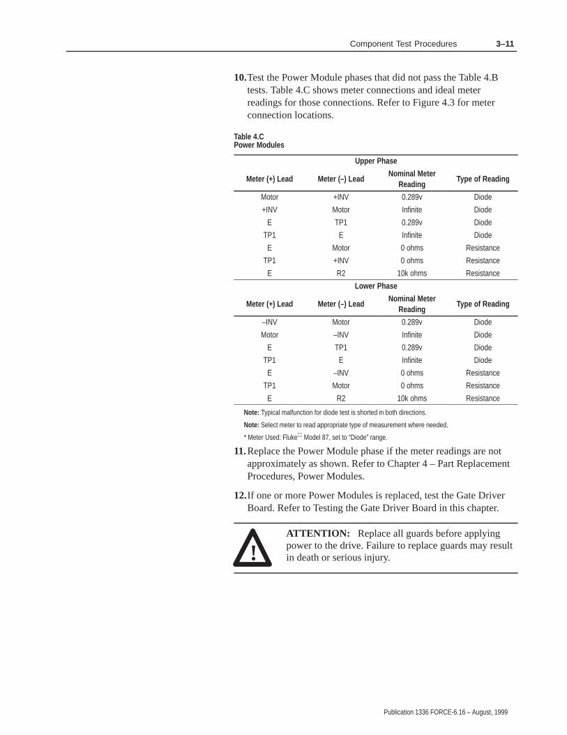
3–11Component Test Procedures
Publication 1336 FORCE-6.16 – August, 1999
10.Test the Power Module phases that did not pass the Table 4.Btests. Table 4.C shows meter connections and ideal meterreadings for those connections. Refer to Figure 4.3 for meterconnection locations.
Table 4.C Power Modules
Upper Phase
Meter (+) Lead Meter (–) LeadNominal Meter
ReadingType of Reading
Motor +INV 0.289v Diode
+INV Motor Infinite Diode
E TP1 0.289v Diode
TP1 E Infinite Diode
E Motor 0 ohms Resistance
TP1 +INV 0 ohms Resistance
E R2 10k ohms Resistance
Lower Phase
Meter (+) Lead Meter (–) LeadNominal Meter
ReadingType of Reading
–INV Motor 0.289v Diode
Motor –INV Infinite Diode
E TP1 0.289v Diode
TP1 E Infinite Diode
E –INV 0 ohms Resistance
TP1 Motor 0 ohms Resistance
E R2 10k ohms Resistance
Note: Typical malfunction for diode test is shorted in both directions.
Note: Select meter to read appropriate type of measurement where needed.
* Meter Used: Fluke Model 87, set to “Diode” range.
11.Replace the Power Module phase if the meter readings are notapproximately as shown. Refer to Chapter 4 – Part ReplacementProcedures, Power Modules.
12.If one or more Power Modules is replaced, test the Gate DriverBoard. Refer to Testing the Gate Driver Board in this chapter.
!ATTENTION: Replace all guards before applyingpower to the drive. Failure to replace guards may resultin death or serious injury.

3–12 Component Test Procedures
Publication 1336 FORCE-6.16 – August, 1999
The Bus Capacitor Bank is located on the upper left side of the MainChassis.
Figure 4.4 Bus Capacitor Bank Test
AB0832A
DC–
DC+
!ATTENTION: Disconnect and lock out power fromthe drive before disassembling the drive. Failure todisconnect power may result in death or serious injury.Verify bus voltage by measuring the voltage betweenthe +DC/–DC Brake Terminals. Do not attempt toservice the drive until the bus voltage has discharged tozero volts.
Test 4 – Testing the BusCapacitors

3–13Component Test Procedures
Publication 1336 FORCE-6.16 – August, 1999
Important: Before you remove connections and wires from thedrive components, mark the connections and wires tocorrespond with their component connections andterminals to prevent incorrect wiring during assembly.
1. Remove power from the drive.
2. Check for zero volts at:
• +DC/–DC Brake Terminals• terminals R-L1, S-L2, and T-L3 on TB1
3. Check for the absence of control voltage at:
• terminals V+ and V– on TB11 on the Main Control Board• TB20 and TB21 on drives using a PLC Comm Adapter Board• TB5, TB6, and TB7 on drives using a Standard Adapter Board• TB3 on drives using a Control Interface L-Option Board
4. Set your meter to test DC voltage.
5. Connect the negative lead of your meter to the –DC BrakeTerminal on TB1 and the positive lead to the +DC BrakeTerminal. Refer to the following tables and Figure 4.4 for meterreadings and terminal locations.
!ATTENTION: Servicing energized industrial controlequipment can be hazardous. Electrical shock, burns,or unintentional actuation of controlled industrialequipment may cause death or serious injury. Followthe safety-related practices of NFPA 70E, ElectricalSafety for Employee Workplaces, when working on ornear energized equipment. Do not work alone onenergized equipment.
6. Apply power AFTER the meter is connected, otherwise yourmeter will read zero volts. Expand readings for all input voltageratings.
Table 4.D Bus Capacitor Bank Test
Drive Rating Input Volts Meter Reading
200 283V DC +/–10%
A 230 325V DC +/–10%
240 339V DC +/–10%
380 537V DC +/–10%
B 415 587V DC +/–10%
480 679V DC +/–10%
500 707V DC +/–10%
C 575 813V DC +/–10%
600 848V DC+/–10%

3–14 Component Test Procedures
Publication 1336 FORCE-6.16 – August, 1999
7. If the voltage is out of tolerance, check the following:
• An open condition at an Input Rectifier.• A voltage drop due to Bus Inductor L1 resistance.• A voltage drop between an Input Rectifier and the bus
capacitors due to loose or resistive wires or connections.• Precharge circuit problems.
8. If the above check does not reveal a problem, replace the BusCapacitor Bank and Load-Sharing Resistors. Refer to Chapter 4 –Part Replacement Procedures, Bus Capacitor Bank.
!ATTENTION: Replace all guards before applyingpower to the drive. Failure to replace guards may resultin death or serious injury.

3–15Component Test Procedures
Publication 1336 FORCE-6.16 – August, 1999
The Input Rectifiers are located on the bottom of the heat sink.
Figure 4.5 Input Rectifier Test
AB0802A
A (–DC Brake)
K (+DC Brake)
AK (AC Input)
K2K1
G2G1
Back
!ATTENTION: Disconnect and lock out power fromthe drive before disassembling the drive. Failure todisconnect power may result in death or serious injury.Verify bus voltage by measuring the voltage betweenthe +DC/–DC Brake Terminals. Do not attempt toservice the drive until the bus voltage has discharged tozero volts.
Important: Before you remove connections and wires from thedrive components, mark the connections and wires tocorrespond with their component connections andterminals to prevent incorrect wiring during assembly.
Test 5 – Testing the InputRectifiers

3–16 Component Test Procedures
Publication 1336 FORCE-6.16 – August, 1999
1. Remove power from the drive.
2. Check for zero volts at:
• +DC/–DC Brake Terminals• terminals R-L1, S-L2, and T-L3 on TB1
3. Check for the absence of control voltage at:
• terminals V+ and V– on TB11 on the Main Control Board• TB20 and TB21 on drives using a PLC Comm Adapter Board• TB5, TB6, and TB7 on drives using a Standard Adapter Board• TB3 on drives using a Control Interface L-Option Board
4. Check for absence of control voltage at:
• TB20 and TB21 on drives using a PLC Comm Adapter Board• TB5, TB6, and TB7 on drives using a Standard Adapter Board
5. Remove the Circuit Board Platform. Refer toChapter 2 – Disassembly and Access Procedures, Removing theCircuit Board Platform.
6. Remove the Input Rectifier Snubber Board. Refer toChapter 2 – Disassembly and Access Procedures, Removing theInput Rectifier Snubber Board.
7. Set your meter to test diodes.
8. The following table shows meter connections and ideal meterreadings for those connections. Refer to Figure 4.5 for meterconnection locations.
Table 4.E Input Rectifier Test
Meter (+) Lead Meter (–) Lead Nominal Meter Reading
AK K Infinite
AK A Infinite
K A Infinite
K AK Infinite
A AK Infinite
A K Infinite
G1 K1 0.011
K1 G1 0.011
G2 K2 0.011
K2 G2 0.011
Note: Typical malfunction is shorted in both directions.
* Meter Used: Fluke Model 87, set to “Diode” range.
9. Replace the Input Rectifier if any meter readings are not asshown. Refer to Chapter 4 – Part Replacement Procedures, InputRectifiers.
10.If the Input Rectifier shorted, check the Power Modules fordamage. Refer to Testing the Power Modules in this chapter.

Chapter 4
Publication 1336 FORCE-6.16 – August, 1999
Part Replacement Procedures
This chapter describes procedures required to replace drivecomponents. This chapter references Chapter 2 – Disassembly andAccess Procedures for basic drive component access.
!ATTENTION: Some printed circuit boards and drivecomponents may contain hazardous voltage levels.Remove power before you disconnect or reconnectwires, and before you remove or replace fuses andcircuit boards. Verify bus voltage by measuring thevoltage between the +DC/–DC Brake Terminals. Donot attempt to service the drive until the bus voltagehas discharged to zero volts.
!ATTENTION: This assembly contains parts andsub-assemblies that are sensitive to electrostaticdischarge. Static control precautions are required whenservicing this assembly. Component damage may resultif you ignore electrostatic discharge control procedures.If you are not familiar with static control procedures,reference Rockwell Automation Publication8000-4.5.2, Guarding Against Electrostatic Discharge,or any other applicable ESD protection handbook.
Chapter Objective
Safety Precautions
Electrostatic DischargePrecautions

4–2 Part Replacement Procedures
Publication 1336 FORCE-6.16 – August, 1999
Electrostatic discharge generated by static electricity can damage thecomplimentary metallic oxide semiconductor devices on variousdrive boards. It is recommended that you perform these proceduresto guard against this type of damage when circuit boards areremoved or installed:
• Wear a wrist-type grounding strap that is grounded to the chassis.
• Attach the wrist strap before removing the new circuit board fromthe conductive packet.
• Remove boards from the drive and immediately insert them intotheir conductive packets.
Tools
You need the following tools to disassemble and assemble the drive:
• Pliers
• Phillips screwdrivers (small, medium, and large)
• Standard screwdrivers (small, medium, and large)
• 25/64-inch or 10 mm socket
• 7/16-inch or 11 mm socket
• 33/64-inch or 13 mm deep-well socket
• 5/16-inch or 8 mm open-end wrench
• Torque wrench, metered in lb-in. or N-m
• Nylon tie wraps
This section explains in detail how to replace the following drivecomponents:
• Bus Capacitor Bank
• Thermistor
• Power Modules
• Bus Fuses F1
• Input Fuses
• Ground Fault CT
• Input Rectifiers
• LEMs
• MOV Surge Suppressor
• Fan and Transformer Assembly
• DC Bus Inductor L1
For Main Control Board, PLC Comm Adapter Board, StandardAdapter Board, Gate Driver Board, Precharge Board, SnubberBoards, and Control Interface Board installation and removalprocedures, refer to Chapter 2.
Major ComponentReplacement

4–3Part Replacement Procedures
Publication 1336 FORCE-6.16 – August, 1999
Rockwell Automation Adjustable Frequency AC Drives are modularby design to enhance troubleshooting and spare parts replacement,thereby helping reduce production down-time.
The following illustration calls out the main components of a typicaldrive. Component designs vary slightly among the different driveratings, but component locations are identical.
Figure 5.1 Main Drive Components
AB0822A
BusCapacitor
Bank
FanTransformer
FanCapacitor
BusInductor L1
GroundSense CT
BusFuse F1
InputFuses (3)
MOV SurgeSuppressor
Power Module GateInterface Board
PowerModule
Input RectifierSnubber Board
Load-SharingResistor
PrechargeBoard Fuses
PrechargeBoard
MountingPlate Gate Driver
BoardLEM
FuseF1
FuseF2
–DC BrakeTerminal
Power Module BusBar
Power ModuleSnubber Board
Thermistor
Main ControlBoard
Control InterfaceL-Option Board
PLC CommAdapter Board
StandardAdapter Board
Control Board/AdapterMounting Plate+DC Brake
Terminal
Detailed ProductIdentification

4–4 Part Replacement Procedures
Publication 1336 FORCE-6.16 – August, 1999
Bus Capacitor Bank
The Bus Capacitor Bank is located on the upper left side of the Main Chassis.
Figure 5.2 Bus Capacitor Bank
AB0787A
(–) BusCapacitor Bar
BusFuses
ConverterFuse Support
Power Module Bus Bar
(+) BusCapacitor Bar
PM SnubberResistors
SnubberResistors Bus Capacitor
Standoffs

4–5Part Replacement Procedures
Publication 1336 FORCE-6.16 – August, 1999
Removal
!ATTENTION: Disconnect and lock out power fromthe drive before disassembling the drive. Failure todisconnect power may result in death or serious injury.Verify bus voltage by measuring the voltage betweenthe +DC/–DC Brake Terminals. Do not attempt toservice the drive until the bus voltage has discharged tozero volts.
!ATTENTION: Wear a wrist-type grounding strapwhen servicing 1336 FORCE Drives. Failure to protectdrive components against ESD may damage drivecomponents. Refer to Electrostatic DischargePrecautions at the beginning of this chapter.
Important: Before you remove connections and wires from thedrive components, mark the connections and wires tocorrespond with their component connections andterminals to prevent incorrect wiring during assembly.
Access the Main Chassis:
1. Remove power from the drive.
2. Check for zero volts at:
• +DC/–DC Brake Terminals• terminals R-L1, S-L2, and T-L3 on TB1
3. Check for absence of control voltage at:
• terminals V+ and V– on TB11 on the Main Control Board• TB20 and TB21 on drives using a PLC Comm Adapter Board• TB5, TB6, and TB7 on drives using a Standard Adapter Board• TB3 on drives using a Control Interface L-Option Board
4. Remove the High Voltage Guard from the drive. Refer toChapter 2 – Disassembly and Access Procedures, Removing theHigh Voltage Guard.
5. Remove the Circuit Board Platform. Refer toChapter 2 – Disassembly and Access Procedures, Removing theCircuit Board Platform.

4–6 Part Replacement Procedures
Publication 1336 FORCE-6.16 – August, 1999
Access the Bus Capacitor Bank:
1. Remove the (+) Bus Capacitor Bar:
A. Remove the two sets of bolts fastening the power cables tothe top and bottom of the Bus Capacitor Bank.
B. Remove the four bolts fastening the Converter Fuse Supportto the (+) Bus Capacitor Bar and Power Module Bus Bar.
C. Pull the Converter Fuse Support, with bus fuses attached,from the drive.
D. Remove the six bolts (2 per phase) fastening the (+) BusCapacitor Bar to the Power Module Bus Bar.
E. Remove the two bolts fastening the (+) Bus Capacitor Bar tothe Bus Capacitor Inverter Standoffs.
F. Remove the three screws fastening the (+) Bus Capacitor Barto the Power Module Snubber Resistors.
G. Pull the (+) Bus Capacitor Bar from the drive.
2. Remove the Power Module Bus Bar:
A. Remove the six screws fastening the Power Module Bus Barto the (–) Bus Capacitor Bar.
B. Remove the eighteen nuts fastening the Power Module BusBars to the (–) Bus Capacitor Bar.
C. Remove the five screws fastening the Power Module Bus Barto the Snubber Resistors.
D. Remove the two bolts fastening the Power Module Bus Barto the drive.
E. Pull the Power Module Bus Bar from the drive.
3. Remove the Bus Capacitors:
A. Remove the eighteen nuts fastening the (–) Bus CapacitorBar to the Bus Capacitors.
B. Pull the (–) Bus Capacitor Bar from the drive.
C. Remove the Bus Capacitors from the drive.

4–7Part Replacement Procedures
Publication 1336 FORCE-6.16 – August, 1999
Installation
1. Fasten the capacitor assembly in reverse order of removal. Referto Chapter 2 – Disassembly and Access Procedures, FastenerTorque Specifications.
Important: Orient the notch and vent hole on the Bus Capacitors tothe top of the drive.
2. Connect the Load-Sharing Resistors to the Bus Capacitorsaccording to the diagram in Figure 5.3. Refer to the schematicdiagrams in this manual for more information on componentconfigurations.
Important: Check the Load-Sharing Resistors for an open conditionand replace any open resistors.
Important: If the drive is equipped with PEM nuts on the Cap Busbar, use them instead of capacitor studs to make theelectrical connection.
Figure 5.3 Load-Sharing Resistor Connections to Bus Capacitors
AB0820A
+
+
++
+ ++
+
R1
C1
C2 C4
C3
C6
C5
C8
C7
C10+
C9+
C12+
C11+
C18+
C14 C16+ +
+C13 C15
+C17
+
!ATTENTION: Capacitors not installed correctly willerupt or vent and could cause injury and equipmentdamage. Observe correct polarities.

4–8 Part Replacement Procedures
Publication 1336 FORCE-6.16 – August, 1999
Thermistor
The Thermistor is located on the heat sink at the top-middle of thedrive.
Figure 5.4 Thermistor
AB0833A
Thermistor
Connector to MainControl Board J1
Removal
!ATTENTION: Disconnect and lock out power fromthe drive before disassembling the drive. Failure todisconnect power may result in death or serious injury.Verify bus voltage by measuring the voltage betweenthe +DC/–DC Brake Terminals. Do not attempt toservice the drive until the bus voltage has discharged tozero volts.

4–9Part Replacement Procedures
Publication 1336 FORCE-6.16 – August, 1999
!ATTENTION: Wear a wrist-type grounding strapwhen servicing 1336 FORCE Drives. Failure to protectdrive components against ESD may damage drivecomponents. Refer to Electrostatic DischargePrecautions at the beginning of this chapter.
Important: Before you remove connections and wires from thedrive components, mark the connections and wires tocorrespond with their component connections andterminals to prevent incorrect wiring during assembly.
1. Remove power from the drive.
2. Check for zero volts at:
• +DC/–DC Brake Terminals• terminals R-L1, S-L2, and T-L3 on TB1
3. Check for absence of control voltage at:
• terminals V+ and V– on TB11 on the Main Control Board• TB20 and TB21 on drives using a PLC Comm Adapter Board• TB5, TB6, and TB7 on drives using a Standard Adapter Board• TB3 on drives using a Control Interface L-Option Board
4. Remove the screws fastening the High Voltage Guard from thedrive. Refer to Chapter 2 – Disassembly and Access Procedures,Removing the High Voltage Guard.
5. Disconnect the Thermistor connector at J1 on the Main ControlBoard.
6. Unscrew the Thermistor from the heat sink.
Installation
Install the Thermistor in reverse order of removal. Refer toChapter 2 – Disassembly and Access Procedures, Fastener TorqueSpecifications.
!ATTENTION: Replace all guards before applyingpower to the drive. Failure to replace guards may resultin death or serious injury.

4–10 Part Replacement Procedures
Publication 1336 FORCE-6.16 – August, 1999
Power Modules
The Power Modules are located near the top of the heat sink. If oneor more Power Modules is replaced, you must check the PowerModule Snubber Board and the Precharge Board. Refer toChapter 2 – Disassembly and Access Procedures, Removing thePrecharge Board.
Figure 5.5 Power Modules
AB0789A
PowerModule
Preform
Screw(6)
Screw(3)
Power ModuleBus Bar
Power ModuleGate Interface
Board
SnubberStandoffs
Output BusBar
Screw(8)
Removal
!ATTENTION: Disconnect and lock out power fromthe drive before disassembling the drive. Failure todisconnect power may result in death or serious injury.Verify bus voltage by measuring the voltage betweenthe +DC/–DC Brake Terminals. Do not attempt toservice the drive until the bus voltage has discharged tozero volts.

4–11Part Replacement Procedures
Publication 1336 FORCE-6.16 – August, 1999
!ATTENTION: Hazard of electric shock exists. Up to1,600 VDC will be on J1 if the Snubber Resistor isopen. Measure for zero (0) VDC from Snubber Boardterminal TP3 to plus (+) bus before removingconnector J1. Use a resistor greater than 1 ohm and lessthan 100 ohm, rated for 25 watts minimum, betweenTP3 and plus (+) bus to discharge any voltage. Refer toChapter 2 – Disassembly and Access Procedures,Removing a Power Module Snubber Board.
!ATTENTION: Wear a wrist-type grounding strapwhen servicing 1336 FORCE Drives. Failure to protectdrive components against ESD may damage drivecomponents. Refer to Electrostatic DischargePrecautions at the beginning of this chapter.
Important: Before you remove connections and wires from thedrive components, mark the connections and wires tocorrespond with their component connections andterminals to prevent incorrect wiring during assembly.
1. Remove power from the drive.
2. Check for zero volts at:
• +DC/–DC Brake Terminals• terminals R-L1, S-L2, and T-L3 on TB1
3. Check for absence of control voltage at:
• terminals V+ and V– on TB11 on the Main Control Board• TB20 and TB21 on drives using a PLC Comm Adapter Board• TB5, TB6, and TB7 on drives using a Standard Adapter Board• TB3 on drives using a Control Interface L-Option Board
4. Remove the High Voltage Guard from the drive. Refer toChapter 2 – Disassembly and Access Procedures, Removing theHigh Voltage Guard.
5. Remove the Circuit Board Platform. Refer toChapter 2 – Disassembly and Access Procedures, Removing theCircuit Board Platform.
6. Remove the six bolts fastening the three Output Bus Bars to thePower Module Assembly and TB1.
7. Remove the Power Module Snubber Boards. Refer toChapter 2 – Disassembly and Access Procedures, Removing aPower Module Snubber Board.

4–12 Part Replacement Procedures
Publication 1336 FORCE-6.16 – August, 1999
8. Remove the bolts fastening the Power Module Bus Bar to the BusCapacitor Bank.
9. Remove the eight screws fastening the Snubber Standoffs to thePower Module Bus Bar. Remove the standoffs.
10.Slide the Power Module Bus Bar to the right and remove the busbar from the drive.
11.Remove the three screws fastening the Power Module InterfaceBoard to the Power Module.
12.Remove the six screws fastening the Power Module to the heatsink.
13.Pull the Power Module away from the heat sink.
Installation
1. Clean all surfaces between the Power Module and the heat sinkusing a soft, clean cloth.
2. Replace the Preform between the Power Module and the heatsink.
3. Install the Power Module in reverse order of removal. Refer toChapter 2 – Disassembly and Access Procedures, Fastener TorqueSpecifications.
Important: Remove the copper shorting strip from the PowerModule before replacing the Power Module InterfaceBoard.
!ATTENTION: Do not substitute longer or shorterhardware when fastening the Power Modulecomponents to the Power Modules. Use the same sizefastener to fasten the components as was originallyused. Using different fastener lengths will damage thePower Modules.
!ATTENTION: Replace all guards before applyingpower to the drive. Failure to replace guards may resultin death or serious injury.

4–13Part Replacement Procedures
Publication 1336 FORCE-6.16 – August, 1999
Bus Fuses F1
The Bus Fuses are located on the Bus Capacitor Bank Assembly.
Figure 5.6 Bus Fuses F1
AB0834A
Bus Fuses
Removal
!ATTENTION: Disconnect and lock out power fromthe drive before disassembling the drive. Failure todisconnect power may result in death or serious injury.Verify bus voltage by measuring the voltage betweenthe +DC/–DC Brake Terminals. Do not attempt toservice the drive until the bus voltage has discharged tozero volts.
4–14 Part Replacement Procedures
Publication 1336 FORCE-6.16 – August, 1999
!ATTENTION: Wear a wrist-type grounding strapwhen servicing 1336 FORCE Drives. Failure to protectdrive components against ESD may damage drivecomponents. Refer to Electrostatic DischargePrecautions at the beginning of this chapter.
Important: Before you remove connections and wires from thedrive components, mark the connections and wires tocorrespond with their component connections andterminals to prevent incorrect wiring during assembly.
1. Remove power from the drive.
2. Check for zero volts at:
• +DC/–DC Brake Terminals• terminals R-L1, S-L2, and T-L3 on TB1
3. Check for absence of control voltage at:
• terminals V+ and V– on TB11 on the Main Control Board• TB20 and TB21 on drives using a PLC Comm Adapter Board• TB5, TB6, and TB7 on drives using a Standard Adapter Board• TB3 on drives using a Control Interface L-Option Board
4. Remove the screws fastening the High Voltage Guard from thedrive. Refer to Chapter 2 – Disassembly and Access Procedures,Removing the High Voltage Guard.
5. Remove the screws fastening the two Bus Fuses to the drive.
6. Pull the fuses out from the drive.
Important: When one fuse blows, you must replace both fuses.Also replace the Bus Fuse Diode Module in parallel.
Installation
Install the Bus Fuses in reverse order of removal. Refer toChapter 2 – Disassembly and Access Procedures, Fastener TorqueSpecifications.
!ATTENTION: Replace all guards before applyingpower to the drive. Failure to replace guards may resultin death or serious injury.

4–15Part Replacement Procedures
Publication 1336 FORCE-6.16 – August, 1999
Input Fuses
The Input Fuses are located on the bottom left-hand side of thechassis above TB1.
Figure 5.7 Input Fuses
AB0795A
InputFuses
Input BusBars
Removal
!ATTENTION: Disconnect and lock out power fromthe drive before disassembling the drive. Failure todisconnect power may result in death or serious injury.Verify bus voltage by measuring the voltage betweenthe +DC/–DC Brake Terminals. Do not attempt toservice the drive until the bus voltage has discharged tozero volts.

4–16 Part Replacement Procedures
Publication 1336 FORCE-6.16 – August, 1999
!ATTENTION: Wear a wrist-type grounding strapwhen servicing 1336 FORCE Drives. Failure to protectdrive components against ESD may damage drivecomponents. Refer to Electrostatic DischargePrecautions at the beginning of this chapter.
Important: Before you remove connections and wires from thedrive components, mark the connections and wires tocorrespond with their component connections andterminals to prevent incorrect wiring during assembly.
1. Remove power from the drive.
2. Check for zero volts at:
• +DC/–DC Brake Terminals• terminals R-L1, S-L2, and T-L3 on TB1
3. Check for absence of control voltage at:
• terminals V+ and V– on TB11 on the Main Control Board• TB20 and TB21 on drives using a PLC Comm Adapter Board• TB5, TB6, and TB7 on drives using a Standard Adapter Board• TB3 on drives using a Control Interface L-Option Board
4. Remove the nuts fastening the Input Fuse to the Input Bus Barand TB1.
5. Pull the blown fuse out from the drive.
Installation
Install the Input Fuse in reverse order of removal. Refer toChapter 2 – Disassembly and Access Procedures, Fastener TorqueSpecifications.
!ATTENTION: Replace all guards before applyingpower to the drive. Failure to replace guards may resultin death or serious injury.

4–17Part Replacement Procedures
Publication 1336 FORCE-6.16 – August, 1999
Ground Fault CT
The Ground Fault CT encircles the Input Bus Bars and is locatedbetween the Input Fuse Assembly and the Input Rectifier Assembly.
Figure 5.8 Ground Fault CT
AB0793A
GroundFault CT
Connector to GateDriver Board J2
Input BusBars
Removal
!ATTENTION: Disconnect and lock out power fromthe drive before disassembling the drive. Failure todisconnect power may result in death or serious injury.Verify bus voltage by measuring the voltage betweenthe +DC/–DC Brake Terminals. Do not attempt toservice the drive until the bus voltage has discharged tozero volts.
4–18 Part Replacement Procedures
Publication 1336 FORCE-6.16 – August, 1999
!ATTENTION: Wear a wrist-type grounding strapwhen servicing 1336 FORCE Drives. Failure to protectdrive components against ESD may damage drivecomponents. Refer to Electrostatic DischargePrecautions at the beginning of this chapter.
Important: Before you remove connections and wires from thedrive components, mark the connections and wires tocorrespond with their component connections andterminals to prevent incorrect wiring during assembly.
1. Remove power from the drive.
2. Check for zero volts at:
• +DC/–DC Brake Terminals• terminals R-L1, S-L2, and T-L3 on TB1
3. Check for absence of control voltage at:
• terminals V+ and V– on TB11 on the Main Control Board• TB20 and TB21 on drives using a PLC Comm Adapter Board• TB5, TB6, and TB7 on drives using a Standard Adapter Board• TB3 on drives using a Control Interface L-Option Board
4. Remove the screws fastening the High Voltage Guard from thedrive. Refer to Chapter 2 – Disassembly and Access Procedures,Removing the High Voltage Guard.
5. Remove the Circuit Board Platform. Refer to Chapter 2 –Disassembly and Access Procedures, Removing the Circuit BoardPlatform.
6. Remove the six screws fastening the Input Rectifier wiring to theInput Bus Bars.
7. Remove the six bolts fastening the Input Bus Bars to the InputRectifier Assembly and the Input Fuse Assembly.
8. Slide the Input Bus Bars to the right to remove the bus bars and theGround Fault CT, which encircles the bus bars, from the drive.
9. Slide the Ground Fault CT off the bus bars.

4–19Part Replacement Procedures
Publication 1336 FORCE-6.16 – August, 1999
Installation
Install the Ground Fault CT in reverse order of removal, inserting theInput Bus Bars through the center of the Ground Fault CT. Refer toChapter 2 – Disassembly and Access Procedures, Fastener TorqueSpecifications.
!ATTENTION: A possible short-circuit hazard exists.Position the fuse-to-inductor wire with theshrink-wrapped end of the wire connected to the BusInductor. Failure to position the wire as illustrated mayresult in serious injury or equipment damage.
!ATTENTION: Replace all guards before applyingpower to the drive. Failure to replace guards may resultin death or serious injury.

4–20 Part Replacement Procedures
Publication 1336 FORCE-6.16 – August, 1999
Input Rectifiers
The Input Rectifiers are located toward the bottom of the heat sink.
Figure 5.9 Input Rectifiers
AB0790A
(–) ConverterBar
(+) ConverterBar
Snubber BoardStandoffs
Preform InputRectifier
Removal
!ATTENTION: Disconnect and lock out power fromthe drive before disassembling the drive. Failure todisconnect power may result in death or serious injury.Verify bus voltage by measuring the voltage betweenthe +DC/–DC Brake Terminals. Do not attempt toservice the drive until the bus voltage has discharged tozero volts.

4–21Part Replacement Procedures
Publication 1336 FORCE-6.16 – August, 1999
!ATTENTION: Wear a wrist-type grounding strapwhen servicing 1336 FORCE Drives. Failure to protectdrive components against ESD may damage drivecomponents. Refer to Electrostatic DischargePrecautions at the beginning of this chapter.
Important: Before you remove connections and wires from thedrive components, mark the connections and wires tocorrespond with their component connections andterminals to prevent incorrect wiring during assembly.
1. Remove power from the drive.
2. Check for zero volts at:
• +DC/–DC Brake Terminals• terminals R-L1, S-L2, and T-L3 on TB1
3. Check for absence of control voltage at:
• terminals V+ and V– on TB11 on the Main Control Board• TB20 and TB21 on drives using a PLC Comm Adapter Board• TB5, TB6, and TB7 on drives using a Standard Adapter Board• TB3 on drives using a Control Interface L-Option Board
4. Remove the High Voltage Guard from the drive. Refer toChapter 2 – Disassembly and Access Procedures, Removing theHigh Voltage Guard.
5. Remove the Circuit Board Platform. Refer toChapter 2 – Disassembly and Access Procedures, Removing theCircuit Board Platform.
6. Remove the Input Rectifier Snubber Boards. Refer toChapter 2 – Disassembly and Access Procedures, Removing anInput Rectifier Snubber Board.
7. Remove the three bolts fastening the Input Bus Bars to the InputRectifiers.
8. Remove the six Allen-head screws fastening the positive andnegative Converter Bus Bars to the Input Rectifiers.
9. Remove the Precharge Wiring Harness from the top of therectifiers.
10.Remove the four screws fastening the Input Rectifier to the heatsink.
11.Pull the Input Rectifier away from the heat sink.

4–22 Part Replacement Procedures
Publication 1336 FORCE-6.16 – August, 1999
Installation
1. Clean all surfaces between the Input Rectifier and the heat sinkusing a soft, clean cloth.
2. Replace the Preform between the Input Rectifier and the heatsink.
3. Install the Input Rectifier in reverse order of removal. Refer toChapter 2 – Disassembly and Access Procedures, Fastener TorqueSpecifications.
!ATTENTION: Replace all guards before applyingpower to the drive. Failure to replace guards may resultin death or serious injury.

4–23Part Replacement Procedures
Publication 1336 FORCE-6.16 – August, 1999
LEMs
The two LEMs are located above TB1 on the right side ofthe chassis.
Figure 5.10 LEMs
AB0796A
LEMScrews (9)
Screws (2)TB1 ShieldOutput
Bus Bars
Removal
!ATTENTION: Disconnect and lock out power fromthe drive before disassembling the drive. Failure todisconnect power may result in death or serious injury.Verify bus voltage by measuring the voltage betweenthe +DC/–DC Brake Terminals. Do not attempt toservice the drive until the bus voltage has discharged tozero volts.

4–24 Part Replacement Procedures
Publication 1336 FORCE-6.16 – August, 1999
!ATTENTION: Hazard of electric shock exists. Up to1,600 VDC will be on J1 if the Snubber Resistor isopen. Measure for zero (0) VDC from Snubber Boardterminal TP3 to plus (+) bus before removingconnector J1. Use a resistor greater than 1 ohm and lessthan 100 ohm, rated for 25 watts minimum, betweenTP3 and plus (+) bus to discharge any voltage. Refer toChapter 2 – Disassembly and Access Procedures,Removing a Power Module Snubber Board.
!ATTENTION: Wear a wrist-type grounding strapwhen servicing 1336 FORCE Drives. Failure to protectdrive components against ESD may damage drivecomponents. Refer to Electrostatic DischargePrecautions at the beginning of this chapter.
Important: Before you remove connections and wires from thedrive components, mark the connections and wires tocorrespond with their component connections andterminals to prevent incorrect wiring during assembly.
1. Remove power from the drive.
2. Check for zero volts at:
• +DC/–DC Brake Terminals• terminals R-L1, S-L2, and T-L3 on TB1
3. Check for absence of control voltage at:
• terminals V+ and V– on TB11 on the Main Control Board• TB20 and TB21 on drives using a PLC Comm Adapter Board• TB5, TB6, and TB7 on drives using a Standard Adapter Board• TB3 on drives using a Control Interface L-Option Board
4. Remove the High Voltage Guard from the drive. Refer toChapter 2 – Disassembly and Access Procedures, Removing theHigh Voltage Guard.
5. Remove the Circuit Board Platform. Refer toChapter 2 – Disassembly and Access Procedures, Removing theCircuit Board Platform.
6. Remove the nine bolts fastening the Output Bus Bars to thePower Module Assembly and TB1.
7. Pull the Output Bus Bars out from the drive.
8. Remove the two screws fastening the TB1 shield to the TB1Assembly.

4–25Part Replacement Procedures
Publication 1336 FORCE-6.16 – August, 1999
9. Pull the TB1 shield away from the drive.
10.Remove the four screws fastening the LEM Interface Board to thestandoffs.
11.Lift the LEM up and away from the drive.
Installation
Install the LEMs in reverse order of removal. Refer toChapter 2 – Disassembly and Access Procedures, Fastener TorqueSpecifications.
!ATTENTION: Replace all guards before applyingpower to the drive. Failure to replace guards may resultin death or serious injury.

4–26 Part Replacement Procedures
Publication 1336 FORCE-6.16 – August, 1999
MOV Surge Suppressor
The MOV Surge Suppressor is located on top of the Fan Cover Plate.The MOV protects the drive from high voltage surges aboveapproximately 1,000 volts. Replace it if it is burned, expanded, orruptured after such events as a lightning strike, or inadvertentconnection of the drive input to a voltage source substantially abovenameplate voltage.
Figure 5.11 MOV Surge Suppressor
AB0797A
MOV SurgeSuppressor
Removal
!ATTENTION: Disconnect and lock out power fromthe drive before disassembling the drive. Failure todisconnect power may result in death or serious injury.Verify bus voltage by measuring the voltage betweenthe +DC/–DC Brake Terminals. Do not attempt toservice the drive until the bus voltage has discharged tozero volts.

4–27Part Replacement Procedures
Publication 1336 FORCE-6.16 – August, 1999
!ATTENTION: Wear a wrist-type grounding strapwhen servicing 1336 FORCE Drives. Failure to protectdrive components against ESD may damage drivecomponents. Refer to Electrostatic DischargePrecautions at the beginning of this chapter.
Important: Before you remove connections and wires from thedrive components, mark the connections and wires tocorrespond with their component connections andterminals to prevent incorrect wiring during assembly.
1. Remove power from the drive.
2. Check for zero volts at:
• +DC/–DC Brake Terminals• terminals R-L1, S-L2, and T-L3 on TB1
3. Check for absence of control voltage at:
• terminals V+ and V– on TB11 on the Main Control Board• TB20 and TB21 on drives using a PLC Comm Adapter Board• TB5, TB6, and TB7 on drives using a Standard Adapter Board• TB3 on drives using a Control Interface L-Option Board
4. Remove the High Voltage Guard from the drive. Refer toChapter 2 – Disassembly and Access Procedures, Removing theHigh Voltage Guard.
5. Remove the Circuit Board Platform. Refer toChapter 2 – Disassembly and Access Procedures, Removing theCircuit Board Platform.
6. Remove the three screws fastening the MOV Surge Suppressorwires to the Input Bus Bars.
7. Remove the screw fastening the MOV Surge Suppressor wire toTB1 terminal PE.
8. Remove the screw fastening the MOV Surge Suppressor to thechassis.
9. Pull the MOV Surge Suppressor from the drive.
Installation
Install the MOV Surge Suppressor in reverse order of removal. Referto Chapter 2 – Disassembly and Access Procedures, Fastener TorqueSpecifications.
!ATTENTION: Replace all guards before applyingpower to the drive. Failure to replace guards may resultin death or serious injury.

4–28 Part Replacement Procedures
Publication 1336 FORCE-6.16 – August, 1999
Fan and Transformer Assembly
The Fan is located in the chassis and under TB1 at the bottom of theheat sink. The Fan Transformer and Fan Capacitor are located in thebottom left corner of the chassis.
Figure 5.12 Fan and Transformer
AB0791A
FanFan
Cover
FanTransformer
TB1
FanCapacitor
TB1 LabelPlate
MOV SurgeSuppressor
Removal
!ATTENTION: Disconnect and lock out power fromthe drive before disassembling the drive. Failure todisconnect power may result in death or serious injury.Verify bus voltage by measuring the voltage betweenthe +DC/–DC Brake Terminals. Do not attempt toservice the drive until the bus voltage has discharged tozero volts.

4–29Part Replacement Procedures
Publication 1336 FORCE-6.16 – August, 1999
!ATTENTION: Hazard of electric shock exists. Up to1,600 VDC will be on J1 if the Snubber Resistor isopen. Measure for zero (0) VDC from Snubber Boardterminal TP3 to plus (+) bus before removingconnector J1. Use a resistor greater than 1 ohm and lessthan 100 ohm, rated for 25 watts minimum, betweenTP3 and plus (+) bus to discharge any voltage. Refer toChapter 2 – Disassembly and Access Procedures,Removing a Power Module Snubber Board.
!ATTENTION: Wear a wrist-type grounding strapwhen servicing 1336 FORCE Drives. Failure to protectdrive components against ESD may damage drivecomponents. Refer to Electrostatic DischargePrecautions at the beginning of this chapter.
Important: Before you remove connections and wires from thedrive components, mark the connections and wires tocorrespond with their component connections andterminals to prevent incorrect wiring during assembly.
Access the Main Chassis:
1. Remove power from the drive.
2. Check for zero volts at:
• +DC/–DC Brake Terminals• terminals R-L1, S-L2, and T-L3 on TB1
3. Check for absence of control voltage at:
• terminals V+ and V– on TB11 on the Main Control Board• TB20 and TB21 on drives using a PLC Comm Adapter Board• TB5, TB6, and TB7 on drives using a Standard Adapter Board• TB3 on drives using a Control Interface L-Option Board
4. Remove the High Voltage Guard from the drive. Refer toChapter 2 – Disassembly and Access Procedures, Removing theHigh Voltage Guard.
5. Remove the Circuit Board Platform. Refer toChapter 2 – Disassembly and Access Procedures, Removing theCircuit Board Platform.
6. Remove the nine bolts fastening the Output Bus Bars to thePower Module Assembly and TB1.
7. Pull the Output Bus Bars away from the drive.
8. Remove the Input Fuses. Refer to the removal instructions forInput Fuses in this chapter.

4–30 Part Replacement Procedures
Publication 1336 FORCE-6.16 – August, 1999
9. Remove the three bolts fastening the Input Bus Bars to the InputRectifier and remove the six screws on the Input Bus Bars.
10.Remove the Input Bus Bars, with the Ground Fault CT encirclingthe bars, from the drive.
11.Remove the MOV Surge Suppressor. Refer to the removalinstructions for the MOV Surge Suppressor in this chapter.
Remove TB1:
1. Remove the nut located on the lowest stud on Terminal PE.
2. Remove the four screws fastening the TB1 Assembly to the drive.
3. Pull the complete TB1 Assembly, with the shield and LEMSattached, away from the drive.
Access the Fan:
1. Disconnect the Fan Wiring Harness.
2. Remove the screws fastening the Fan Cover to the chassis.
3. Pull the Fan Cover assembly away from the drive.
4. Remove the screws fastening the fan to the Fan Cover to removethe fan.
5. Disconnect the Fan Capacitor from the Fan Wiring Harness.
6. Unscrew the Fan Capacitor from the chassis by hand.
7. Disconnect the Fan Transformer from the Fan Wiring Harness.
8. Remove the screws fastening the Fan Transformer to the chassis.
Installation
Install the Fan Assembly in reverse order of removal, with thefollowing exceptions:
• Thread the fan wiring connector through the hole in the FanCover.
• Refer to Chapter 2 – Disassembly and Access Procedures,Fastener Torque Specifications.
• Install the Fan Capacitor to the chassis with M8 split washer andhand tighten.
• Connect the Fan Transformer red wire to TB1 terminal S-L2 andthe black wire to TB1 terminal R-L1.

4–31Part Replacement Procedures
Publication 1336 FORCE-6.16 – August, 1999
Important: Install washers on TB1 terminals with the serratedside up.
!ATTENTION: Replace all guards before applyingpower to the drive. Failure to replace guards may resultin death or serious injury.

4–32 Part Replacement Procedures
Publication 1336 FORCE-6.16 – August, 1999
DC Bus Inductor L1
DC Bus Inductor L1 is located at the bottom of the drive.
Figure 5.13 DC Bus Inductor L1
AB0792A
DC BusInductor L1
–DC BrakeTerminal
+DC BrakeTerminal
L1
L4
L2
L3
Removal
!ATTENTION: Disconnect and lock out power fromthe drive before disassembling the drive. Failure todisconnect power may result in death or serious injury.Verify bus voltage by measuring the voltage betweenthe +DC/–DC Brake Terminals. Do not attempt toservice the drive until the bus voltage has discharged tozero volts.

4–33Part Replacement Procedures
Publication 1336 FORCE-6.16 – August, 1999
!ATTENTION: Wear a wrist-type grounding strapwhen servicing 1336 FORCE Drives. Failure to protectdrive components against ESD may damage drivecomponents. Refer to Electrostatic DischargePrecautions at the beginning of this chapter.
Important: Before you remove connections and wires from thedrive components, mark the connections and wires tocorrespond with their component connections andterminals to prevent incorrect wiring during assembly.
1. Remove power from the drive.
2. Check for zero volts at:
• +DC/–DC Brake Terminals• terminals R-L1, S-L2, and T-L3 on TB1
3. Check for absence of control voltage at:
• terminals V+ and V– on TB11 on the Main Control Board• TB20 and TB21 on drives using a PLC Comm Adapter Board• TB5, TB6, and TB7 on drives using a Standard Adapter Board• TB3 on drives using a Control Interface L-Option Board
4. Disconnect AC input and motor output wiring from TB1 toprovide easy access to the DC Bus Inductor enclosure.
!ATTENTION: The DC Bus Inductor weighs 100 lbs.Failure to use extreme caution in handling this partmay result in serious injury.
5. Remove the eight bolts fastening the Bus Bar Cables to the DCBus Inductor terminals.
6. Remove the four bolts fastening the DC Bus Inductor to the backpanel of the chassis.
7. Remove the Bus Inductor from the drive.

4–34 Part Replacement Procedures
Publication 1336 FORCE-6.16 – August, 1999
Installation
Install DC Bus Inductor L1 in reverse order of removal. Refer toChapter 2 – Disassembly and Access Procedures, Fastener TorqueSpecifications.
!ATTENTION: If you mount the inductor remotely,verify the connections between the Bus Inductor, theInput Rectifier Bus Bars and the DC Brake Terminals.L1 of inductor should connect to the (+) Input RectifierBus Bar, L2 to the +DC Brake Terminal, L3 to the –DCBrake Terminal, and L4 to the (–) Input Rectifier BusBar. Refer to Chapter 3 – Component Test Procedures,Test 5 – Testing the Input Rectifiers.
!ATTENTION: Replace all guards before applyingpower to the drive. Failure to replace guards may resultin death or serious injury.
Chapter 5
Publication 1336 FORCE-6.16 – August, 1999
Replacement Parts List
This chapter illustrates and lists replacement parts for the 1336FORCE Drives rated BP300 – BP450, and describes replacementparts ordering procedures.
The following illustration and table show you parts, part names, partnumbers, locations, and chapters for replacement procedures.
For your convenience, the Rockwell Automation Drives Divisionand the Rockwell Automation Support Division provide efficient andconvenient repair and exchange for eligible equipment.
A product service report number is required to return any equipmentfor repair. Your local Rockwell Automation distributor or area salesand support office can provide you with a product service reportnumber.
You should return equipment to be repaired to the area sales andsupport center nearest you. Reference the product service reportnumber on the carton and packing slip. Include:
• Your company name
• Your company address
• The repair purchase order number
• A brief description of the problem
Contact your local Rockwell Automation distributor or sales officefor a complete listing of area sales and support centers near you.
For parts catalog numbers, refer to the 1336 FORCE Spare PartsPricing publication included with your drive documentation set.
Chapter Objectives
Ordering ReplacementParts

5–2 Replacement Parts List
Publication 1336 FORCE-6.16 – August, 1999
Figure 6.1 Parts for BP300 – BP450 Drives
11
2312
13
AB0823A
21
16
17
18
20
2215
2
1
9
7
24
108
64
3
5
14
19
Replacement Parts Listing
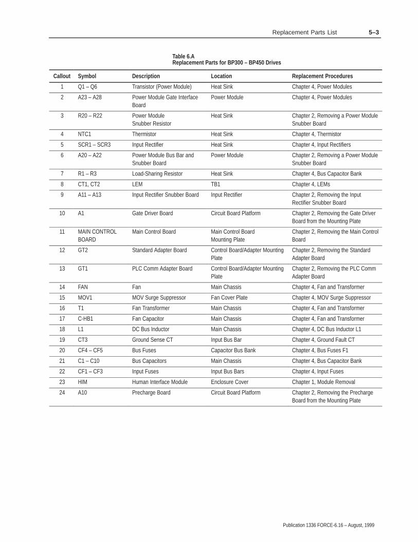
5–3Replacement Parts List
Publication 1336 FORCE-6.16 – August, 1999
Table 6.A Replacement Parts for BP300 – BP450 Drives
Callout Symbol Description Location Replacement Procedures
1 Q1 – Q6 Transistor (Power Module) Heat Sink Chapter 4, Power Modules
2 A23 – A28 Power Module Gate InterfaceBoard
Power Module Chapter 4, Power Modules
3 R20 – R22 Power ModuleSnubber Resistor
Heat Sink Chapter 2, Removing a Power ModuleSnubber Board
4 NTC1 Thermistor Heat Sink Chapter 4, Thermistor
5 SCR1 – SCR3 Input Rectifier Heat Sink Chapter 4, Input Rectifiers
6 A20 – A22 Power Module Bus Bar andSnubber Board
Power Module Chapter 2, Removing a Power ModuleSnubber Board
7 R1 – R3 Load-Sharing Resistor Heat Sink Chapter 4, Bus Capacitor Bank
8 CT1, CT2 LEM TB1 Chapter 4, LEMs
9 A11 – A13 Input Rectifier Snubber Board Input Rectifier Chapter 2, Removing the InputRectifier Snubber Board
10 A1 Gate Driver Board Circuit Board Platform Chapter 2, Removing the Gate DriverBoard from the Mounting Plate
11 MAIN CONTROLBOARD
Main Control Board Main Control BoardMounting Plate
Chapter 2, Removing the Main ControlBoard
12 GT2 Standard Adapter Board Control Board/Adapter MountingPlate
Chapter 2, Removing the StandardAdapter Board
13 GT1 PLC Comm Adapter Board Control Board/Adapter MountingPlate
Chapter 2, Removing the PLC CommAdapter Board
14 FAN Fan Main Chassis Chapter 4, Fan and Transformer
15 MOV1 MOV Surge Suppressor Fan Cover Plate Chapter 4, MOV Surge Suppressor
16 T1 Fan Transformer Main Chassis Chapter 4, Fan and Transformer
17 C-HB1 Fan Capacitor Main Chassis Chapter 4, Fan and Transformer
18 L1 DC Bus Inductor Main Chassis Chapter 4, DC Bus Inductor L1
19 CT3 Ground Sense CT Input Bus Bar Chapter 4, Ground Fault CT
20 CF4 – CF5 Bus Fuses Capacitor Bus Bank Chapter 4, Bus Fuses F1
21 C1 – C10 Bus Capacitors Main Chassis Chapter 4, Bus Capacitor Bank
22 CF1 – CF3 Input Fuses Input Bus Bars Chapter 4, Input Fuses
23 HIM Human Interface Module Enclosure Cover Chapter 1, Module Removal
24 A10 Precharge Board Circuit Board Platform Chapter 2, Removing the PrechargeBoard from the Mounting Plate

5–4 Replacement Parts List
Publication 1336 FORCE-6.16 – August, 1999
This Page Intentionally Left Blank.

Chapter 6
Publication 1336 FORCE-6.16 – August, 1999
Schematics — 250 – 450 HP 1336FORCE Drives

6–2 Schematics — 250 – 450 HP 1336 FORCE Drives
Publication 1336 FORCE-6.16 – August, 1999
AB0813A
12
CT3
CAP BANKS–L2
T–L3
R–L1CF1
CF2
CF3
ACINPUT
POWER50/60HZ
A11 A12 A13
CONVSNUBBER
A10 PRECHARGEBOARD
STANDARD
1110987J3
1
4
CONVSNUBBER
CONVSNUBBER
CNV–
MOV1
PE
TO BLOWERCIRCUIT
PM1
SCR1
SCR4
PM2
SCR6
SCR3
PM3
SCR2
SCR5
DC
+
DC
–
J41 4
S2K
S2G
R2K
R2G
J210 69
T2K
T2G
15 2
R1G
R1K
5
S1G
4
S1K
3
T1G
2
T1K
16
J1
F1 F2 F3
G1
K1 K1
G1
K1
G1
K2
G2
K2
G2
K2
G2
TE
PE
+DC
–DC
(L2)(L1)
(L3)(L4)
+DC
–DC
CF5
R11 R12 R13
SEE NOTE 2
CF4
+DC +INV
(2) (3)
D1
USER BRAKEPOWER
TB9
JUMPER
PE
TE
480VOUT 1
480VOUT 2
480VOUT 3
AUX. ACPOWEROUTPUT
CH1
CNV+
–15V+15V
–SMPS
+SMPS
+5V/CHARGEAC LINE
COMMON
SEE NOTE 5
SEE NOTE 5SEE NOTE 3

6–3Schematics — 250 – 450 HP 1336 FORCE Drives
Publication 1336 FORCE-6.16 – August, 1999
AB0812A
TOMAINCONTROLBOARD
A26
A23
A27
A24
A28
Ek
A25
Ck
Q1 Q3 Q5
Q2Q6Q4
CT14000:1 CT2
4000:1
U–M1
V–M2
W–M3
ACOUTPUTPOWER
G1
23
121
3
GATEINTERFACE
GATEINTERFACE
GATEINTERFACE
INVE
RTER
A20
SNU
BBER
–SMPS
/CHARGEAC LINE
+5VCOMMON
–15V+15V
+SMPS
CVE
RIF
Y36
W_P
OS–
DG
ND
DG
ND
DG
ND
DG
ND
W_P
OS+
V_N
EG+
V_PO
S+U
_NEG
+U
_PO
S+
V_N
EG–
V_PO
S–U
_NEG
–U
_PO
S–W
_NEG
+
TO MAIN CONTROL BOARD
W_A
MPS
–W
_AM
PS+
U_A
MPS
–U
_AM
PS+
W_N
EG–
NEG
_BU
SV_
CO
M N
CW
_VO
LTS
V_VO
LTS
U_V
OLT
S
POS_
BUS
NEG
_CAP
PILO
TEE
_CS
EE_S
KEE
_IO
15
2
12
TB41
21 3 4
J943
56
1075 6 8 9 11 12 13 14
J10
–BU
S
ACT2
ACT1
12
9
J2
+BU
S
+15
–15
+15
INTE
RLO
CK
181716 2019 232221 2524 31
J1
27 2826 3029 32 33 34 35
5
U_A
MPS
–15V
WN
_GAT
EW
N_E
MIT
UN
_GAT
EVN
_EM
ITVN
_GAT
E
1 2 3
UN
_EM
IT
WP_
GAT
EW
P_EM
ITW
N_C
OL
6
DG
ND
+15V
+15V+5V
+5V
+5V
ISO
12R
TNIS
O12
V+2
4V–1
5V–1
5V +5V
+5V
DG
ND
47393837 4140 4442 43 45 46 48 49 50
TB7
VN_C
OL
VP_G
ATE
VP_E
MIT
UP_
EMIT
UP_
GAT
E
UN
_CO
L
J8
WP_
CO
LVP
_CO
LU
P_C
OL
2TB5
65
4
34
1 3
1J13
1
A22
5 E
J1
4 G
1 C
Ek
Ck
G1
5 E
J1
4 G
1 C
Ek
Ck
5 E
J1
4
1 C
GATEINTERFACE
Ek
Ck
G1
5 E
J1
4 G
1 C
GATEINTERFACE
GATEINTERFACE
Ek
Ck
G1
5 E
J1
4 G
1 C
Ek
Ck
G1
5 E
J1
4 G
1 C
TE
R20 R21
INVE
RTER
A21
SNU
BBER
R22
J6 J7421 1 4
NTC1
8 7 6 5 4 3 2 1
PE
16 17 1811 13126 871 32
+15U_AMPS
–15
F3
SEE NOTE 3
A1GATEDRIVERBOARD
1 2
TB6
F1
+15W_AMPS
–15
+INV
–DC
74103–281
R23 R24 R25
G G1
INVE
RTER
SNU
BBER
GN
D_S
HO
RT
DES
ATAC
LIN
E/C
HAR
GE
W_A
MPS
SEE NOTE 4

6–4 Schematics — 250 – 450 HP 1336 FORCE Drives
Publication 1336 FORCE-6.16 – August, 1999
AB0814A
74103–281
+
+
++
+ +
DETAIL 1 – 380/460 VAC
+
+
R1
C1
C2 C4
C3
C6
C5
C8
C7
C10+
C9+
R–L1
(415) (380)
AC–INPUT POWERSEE TABLE 2
S–L2
HEATSINKBLOWER
C–HB1
(0V)
(115V)250 VA
(460)
380/460VAC
T1
NOTES: – DETAIL 1:
1. C1 THRU C18 ARE 400 VDC CAPACITORS.
C12+
C11+
C18+
C14 C16+ +
+C13 C15
+C17
+
Q1 Q3 Q5
CT14000:1
CT24000:1
U–M1
V–M2
W–M3
AC
23
121
3
Ek
A25
Ck
G1
GATEINTERFACE
5 E
J1
4 G
1 C
Ek
A24
Ck
G1
GATEINTERFACE
5 E
J1
4 G
1 C
Ek
A23
Ck
G1
GATEINTERFACE
5 E
J1
4 G
1 C
PE+15U_AMPS
–15
+15W_AMPS
–15
+INV
OUTPUTPOWER
NOTE 4. COMMON MODE CHOKE OPTIONAL EQUIPMENT. PER APPLICATION
R20 R21 R22

6–5Schematics — 250 – 450 HP 1336 FORCE Drives
Publication 1336 FORCE-6.16 – August, 1999
The maximum and minimum wire size accepted by TB9 is 4.0 and 0.8 mm (12 and 18 AWG).Use copper wire only with a minimum temperature rating of 75�C. Maximum Torque is 0.90 – 1.81 N-m (8 – 16 lb-in.).
The auxiliary circuit can be utilized to a maximum current capacity of 8 amperes RMS.
Attention: The installation of auxiliary circuits must comply with the national codes andstandards (NEC, VDE, BSA, etc.) and local codes regarding wire type, conductor size,branch circuit protection and disconnect devices. Failure to do so may result in personalinjury and/or equipment damage.
Note 5: The Output Terminal Block (TB9) is only available on F Frame drives. This terminal block provides a three-phase, high voltage connection from the load side of the AC Input Line Fuses. Normally this connection is used to power an external control transformer (user supplied) or other auxiliary circuit. Refer to Figure 1.1 for location.
Note 3: The following is a listing of all printed circuit assemblies versus fuse and documentation information.
AB0815A
ITEM B/M DIAGRAMSCHEMATIC
A1
A10A11–13A20–22A23–28
380/460VAC FUSE CURRENT/TYPEHORSEPOWER
300
350
DESIGNATOR RATING TYPE P/N
FUSE INFORMATION
74101–399–XX 74101–167
74101–181–5174103–867–5174103–784–5174103–845–51
74101–17974103–86674103–78374103–844
F1–F3 1.5A/600V KTK–R–1.5F3F1
1.5A/600V KTK–R–1.51.0A/600V KTK–R–1
NONENONENONE
25172–260–0825172–260–0925172–260–09
FUSE INFORMATIONRATING TYPE P/N
400
500A
600A
600A
450 700A
25178–315–18450A A70QS250
25178–315–19
25178–315–20
25178–315–20
25178–315–21
FUSE INFORMATION
380/460VAC FUSE CURRENT/TYPE
RATING
ALL 2 x 450A
HORSEPOWER
P/NCATALOG
25178–254–01
A70QS
A70QS
A70QS
A70QS
A65C450–4AB
Note 2: The Inverter Bus Fuse for this product is as follows:
Note 1: The Input Line Fuses for this product are supplied in the unit as follows:
Important: Depending on the circuitry connected, additional fusing may be required.

6–6 Schematics — 250 – 450 HP 1336 FORCE Drives
Publication 1336 FORCE-6.16 – August, 1999
This Page Intentionally Left Blank.

Publication 1336 FORCE-6.16 – August, 1999
A
Adapter Locations, 1–12
Audience for this Manual, P–1
Auxiliary Input, Definition, P–6
Auxiliary Interlock, Definition, P–6
B
Bit, Definition, P–6
Bus Capacitor BankIllustration, 4–4Installation, 4–7Removal, 4–5Test, 3–12
Bus FuseIllustration, 4–13Installation, 4–14Removal, 4–13
Bus Inductor. See DC Bus Inductor L1
C
Check, Definition, P–6
Circuit Board PlatformIllustration, 2–9Installation, 2–11Removal, 2–9
Component Test Procedures, 3–1
Connector, Definition, P–6
Control Board/Adapter Mounting PlateIllustration, 2–19Installation, 2–20Removal, 2–19
Control Interface L-Option BoardAvailable Inputs, 1–5Definition, P–7Illustration, 2–7Installation, 2–8Jumper Locations, 1–4Options, 1–3Removal, 2–7
Control Interface Option, 1–3
Control Logic Wiring and Adapters, 1–1
Conventions in this Manual, P–6
D
DC (+/–) Brake Terminals, 3–8, 3–12, 4–3
DC Bus Inductor L1Illustration, 4–32Installation, 4–34Removal, 4–32
Default, Definition, P–7
Disassembly and Access Procedures, 2–1
DriveEnclosure Type, P–5Identification, P–4Illustration, 4–3Nameplate Location, P–3Rating, P–5
Drive Tools, 1–16
E
Electrostatic Discharge, P–2
Enable Input, Definition, P–7
Enclosure Type, P–5
ESD, P–2
F
False, Definition, P–7
Fan and TransformerIllustration, 4–28Installation, 4–30Removal, 4–28
Fastener Torque Specifications, 2–2
Firmware, Function, 1–16
Four-Point Mounting, 2–3
G
Gate Driver BoardIllustration, 2–21Installation, 2–23Removal, 2–21Test, 3–3
Graphic Programming Terminal (GPT),Description, 1–15
Index

IndexI–2
Publication 1336 FORCE-6.16 – August, 1999
Ground Fault CTIllustration, 4–17Installation, 4–19
H
High Voltage GuardIllustration, 2–5Installation, 2–6Removal, 2–6
HIM. See Human Interface Module
Human Interface Module (HIM)Adapter Locations, 1–12Description, 1–11Illustration, 1–11Operation, 1–14Removal, 1–13
I
Identification, Product, P–3
Input FusesIllustration, 4–15Installation, 4–16
Input ModeProgramming, 1–5Selection, 1–6Three-Wire, Multi-Source, 1–7Two-Wire, Single-Source, 1–7
Input RectifierIllustration, 4–20Installation, 4–22Removal, 4–20Test, 3–15
Input Rectifier Snubber BoardIllustration, 2–29Installation, 2–30Removal, 2–29
Inputs, Available, 1–5
Installation Procedures. See Procedures
J
Jumper, Locations, 1–4
Jumper, Definition, P–7
L
LEMsIllustration, 4–23Installation, 4–25Removal, 4–23
Load Sharing Resistor Connections, 4–7
Local Programming, 1–5
L-Option Board. See Control InterfaceL-Option Board
M
Main Control BoardIllustration, 2–12Installation, 2–14Removal, 2–13
Major Component Replacement. SeeProcedures
ManualAudience, P–1Conventions, P–6Objective, P–1Related Publications, P–8
MountingFour-Point, 2–3Six-Point, 2–3Two-Point, 2–3
MOV Surge SuppressorIllustration, 4–26Installation, 4–27Removal, 4–26
N
Nameplate Location, P–3
O
Objective of this Manual, P–1
Operation, Human Interface Module, 1–14
OptionControl Interface, 1–3Identification, P–4
P
Parameter, Definition, P–7
PLC Comm Adapter BoardIllustration, 2–17Installation, 2–18Reference Signal Connections, 1–9Removal, 2–17Terminal Block Locations, 1–2
Power ModuleIllustration, 4–10Installation, 4–12

Index I–3
Publication 1336 FORCE-6.16 – August, 1999
Removal, 4–10Test, 3–8
Power Module Snubber BoardIllustration, 2–26Installation, 2–28Removal, 2–26
PrecautionsElectrostatic Discharge, P–2Safety, P–1
Precharge BoardIllustration, 2–24Installation, 2–25Removal, 2–24Test, 3–6
Press, Definition, P–7
ProceduresAccessing Internal Drive Components,
2–1Bus Capacitor Bank Installation, 4–7Bus Capacitor Bank Removal, 4–5Bus Capacitor Bank Test, 3–12Bus Fuse Installation, 4–14Bus Fuse Removal, 4–13Circuit Board Platform Installation, 2–11Circuit Board Platform Removal, 2–9Component Test, 3–1Control Board/Adapter Mounting Plate
Installation, 2–20Control Board/Adapter Mounting Plate
Removal, 2–19Control Interface L-Option Board
Installation, 2–8Control Interface L-Option Board
Removal, 2–7DC Bus Inductor L1 Installation, 4–34DC Bus Inductor L1 Removal, 4–32Fan Installation, 4–30Fan Removal, 4–28Gate Driver Board Installation, 2–23Gate Driver Board Removal, 2–21Gate Driver Board Test, 3–3Ground Fault CT Installation, 4–19Ground Fault CT Removal, 4–17High Voltage Guard Installation, 2–6High Voltage Guard Removal, 2–6Input Fuse Installation, 4–16Input Fuse Removal, 4–15Input Rectifier Installation, 4–22Input Rectifier Removal, 4–20Input Rectifier Snubber Board Installation,
2–30Input Rectifier Snubber Board Removal,
2–29Input Rectifier Test, 3–15LEM Installation, 4–25LEM Removal, 4–23
Main Control Board Installation, 2–14Main Control Board Removal, 2–13Major Component Replacement, 4–2MOV Surge Suppressor Installation, 4–27MOV Surge Suppressor Removal, 4–26PLC Comm Adapter Board Installation,
2–18PLC Comm Adapter Board Removal,
2–17Power Module Installation, 4–12Power Module Removal, 4–10Power Module Snubber Board Installation,
2–28Power Module Snubber Board Removal,
2–26Power Module Test, 3–8Precharge Board Installation, 2–25Precharge Board Removal, 2–24Precharge Board Test, 3–6Replacement Part, 4–1Standard Adapter Board Installation,
2–16Standard Adapter Board Removal, 2–15Thermistor Installation, 4–9Thermistor Removal, 4–8
Product Identification, P–3, 4–3
ProgrammingInput Mode, 1–5Local, 1–5
R
Rating, Drive, P–5
Related Publications, P–8
Removal Procedures. See Procedures
Removal, HIM, 1–13
Replacement Part Procedures, 4–1
Replacement Parts List, 5–1
S
Safety Precautions, P–1
Schematics, 6–1
Six-Point Mounting, 2–3
Snubber Board, Input RectifierIllustration, 2–29Installation, 2–30Removal, 2–29
Snubber Board, Power ModuleIllustration, 2–26Installation, 2–28Removal, 2–26

IndexI–4
Publication 1336 FORCE-6.16 – August, 1999
Speed Select, Input State, 1–9
Standard Adapter BoardIllustration, 2–15Installation, 2–16Removal, 2–15Terminal Block Locations, 1–2
T
TB3 Terminal Designations, 1–6
Terminal Block Locations, 1–2
Terminal Designations, TB3, 1–6
ThermistorIllustration, 4–8Installation, 4–9Removal, 4–8
Tools, Required for Service, 2–2, 3–2, 4–2
TorqueFour-Point Mounting Sequence, 2–3Maximum for TB Terminals, 1–6Six-Point Mounting Sequence, 2–3Specifications, 2–3Two-Point Mounting Sequence, 2–3
Troubleshooting, Component TestProcedures, 3–1
True, Definition, P–8
Two-Point Mounting, 2–3
W
Wire Sizes, 1–6

Notes
Publication 1336 FORCE-6.16 – August, 1999

N–2
Publication 1336 FORCE-6.16 – August, 1999

CU
T AL
ON
G D
OTT
ED L
INE
✁We Want Our Manuals to be the Best!
You can help! Our manuals must meet the needs of you, the user. This is your opportunity to make sure they do just that.By filling out this form you can help us provide the most useful, thorough, and accurate manuals available. Please take afew minutes to tell us what you think. Then mail or FAX this form.
FAX: to your local Rockwell Automation/Allen-Bradley Sales Office or 414/512-8579
PUBLICATION NAME
PUBLICATION NUMBER, DATE AND PART NUMBER (IF PRESENT)
✓ CHECK THE FUNCTION THAT MOST CLEARLY DESCRIBES YOUR JOB.
� SUGGEST / RESPONSIBLE FOR THE PURCHASE OF EQUIPMENT � MAINTAIN / OPERATE PROGRAMMABLE MACHINERY
� DESIGN / IMPLEMENT ELECTRICAL SYSTEMS � TRAIN/EDUCATE MACHINE USERS
� SUPERVISE FLOOR OPERATIONS
✓ WHAT LEVEL OF EXPERIENCE DO YOU HAVE WITH EACH OF THE FOLLOWING PRODUCTS?
NONE LITTLE MODERATE EXTENSIVE
PROGRAMMABLE CONTROL � � � �
AC / DC DRIVES � � � �
PERSONAL COMPUTERS � � � �
NC / CNC CONTROLS � � � �
DATA COMMUNICATIONS / LAN � � � �
✓ RATE THE OVERALL QUALITY OF THIS MANUAL BY CIRCLING YOUR RESPONSE BELOW. (1) = POOR (5) = EXCELLENT
HELPFULNESS OF INDEX / TABLE OF CONTENTS 1 2 3 4 5
CLARITY 1 2 3 4 5
EASE OF USE 1 2 3 4 5
ACCURACY AND COMPLETENESS 1 2 3 4 5
QUALITY COMPARED TO OTHER COMPANIES’ MANUALS 1 2 3 4 5
QUALITY COMPARED TO OTHER ALLEN-BRADLEY MANUALS 1 2 3 4 5
✓ WHAT DID YOU LIKE MOST ABOUT THIS MANUAL?
✓ WHAT DID YOU LIKE LEAST ABOUT THIS MANUAL?
✓ PLEASE LIST ANY ERRORS YOU FOUND IN THIS MANUAL (REFERENCE PAGE, TABLE, OR FIGURE NUMBERS).
✓ DO YOU HAVE ANY ADDITIONAL COMMENTS?
✓ COMPLETE THE FOLLOWING.
NAME COMPANY
TITLE DEPARTMENT
STREET CITY STATE ZIP
TELEPHONE DATE

FOLD HERE
FOLD HERE
NO POSTAGENECESSARY
IF MAILEDIN THE
UNITED STATES
BUSINESS REPLY MAILPERMIT NO. 413 MEQUON, WI
POSTAGE WILL BE PAID BY ADDRESSEE
ALLEN-BRADLEYAttn: Marketing CommunicationsP.O. Box 760Mequon, WI 53092-9907
FIRST CLASS

SCANport is a trademark of Rockwell Automation Company, Inc.
PLC is a registered trademark of Rockwell Automation Company, Inc.
Allen-Bradley, a Rockwell Automation Business, has been helping its customers improve pro-ductivity and quality for more than 90 years. We design, manufacture and support a broad rangeof automation products worldwide. They include logic processors, power and motion controldevices, operator interfaces, sensors and a variety of software. Rockwell is one of the world’sleading technology companies.
Worldwide representation.Argentina • Australia • Austria • Bahrain • Belgium • Brazil • Bulgaria • Canada • Chile • China, PRC • Colombia • Costa Rica • Croatia • Cyprus • Czech Republic •Denmark • Ecuador • Egypt • El Salvador • Finland • France • Germany • Greece • Guatemala • Honduras • Hong Kong • Hungary • Iceland • India • Indonesia • Ireland • Israel • Italy • Jamaica • Japan • Jordan • Korea • Kuwait • Lebanon • Malaysia • Mexico • Netherlands • New Zealand • Norway • Pakistan • Peru •Philippines • Poland • Portugal • Puerto Rico • Qatar • Romania • Russia–CIS • Saudi Arabia • Singapore • Slovakia • Slovenia • South Africa, Republic • Spain •Sweden • Switzerland • Taiwan • Thailand • Turkey • United Arab Emirates • United Kingdom • United States • Uruguay • Venezuela • Yugoslavia
Allen-Bradley Headquarters, 1201 South Second Street, Milwaukee, WI 53204 USA, Tel: (1) 414 382-2000 Fax: (1) 414 382-4444
Publication 1336 FORCE-6.16 – August, 1999Supersedes March, 1998
PN 184163(A)Copyright 1998 Allen-Bradley Company, Inc., a Rockwell International Company Printed in USA