sara-n2 series - u-blox · sara-n2 series power-optimized nb-iot (lte cat nb1) modules system...
TRANSCRIPT
SARA-N2 series Power-optimized NB-IoT (LTE Cat NB1) modules System Integration Manual
Abstract This document describes the features and the system integration of the SARA-N2 series NB-IoT
modules. These modules are a complete and cost efficient solution offering single-band and
dual-band data transmission for the Internet of Things technology in the compact SARA form factor.
www.u-blox.com
UBX-17005143 - R04

SARA-N2 series - System Integration Manual
UBX-17005143 - R04 Page 2 of 79
Document Information
Title SARA-N2 series
Subtitle Power-optimized NB-IoT (LTE Cat NB1) modules
Document type System Integration Manual
Document number UBX-17005143
Revision and date R04 22-Jun-2018
Disclosure Restriction
Product status Corresponding content status
Functional Sample Draft For functional testing. Revised and supplementary data will be published later.
In Development /
Prototype
Objective Specification Target values. Revised and supplementary data will be published later.
Engineering Sample Advance Information Data based on early testing. Revised and supplementary data will be published later.
Initial Production Early Production Information Data from product verification. Revised and supplementary data may be published later.
Mass Production /
End of Life
Production Information Document contains the final product specification.
This document applies to the following products:
Product name Type number Modem version Application version PCN reference Product status
SARA-N200 SARA-N200-02B-00 06.57 A07.03 UBX-18005015 Initial Production
SARA-N201 SARA-N201-02B-00 06.57 A07.03 UBX-18005015 End of Life
SARA-N201-02B-01 06.57 A08.05 UBX-18023224 Initial Production
SARA-N210 SARA-N210-02B-00 06.57 A07.03 UBX-18005015 Initial Production
SARA-N211 SARA-N211-02X-00 06.57 A07.03 UBX-18005015 Initial Production
SARA-N280 SARA-N280-02B-00 06.57 A07.03 UBX-18005015 Initial Production
u-blox or third parties may hold intellectual property rights in the products, names, logos and designs included in this
document. Copying, reproduction, modification or disclosure to third parties of this document or any part thereof is only
permitted with the express written permission of u-blox.
The information contained herein is provided “as is” and u-blox assumes no liability for its use. No warranty, either express or
implied, is given, including but not limited to, with respect to the accuracy, correctness, reliability and fitness for a particular
purpose of the information. This document may be revised by u-blox at any time without notice. For the most recent
documents, visit www.u-blox.com.
Copyright © u-blox AG.
SARA-N2 series - System Integration Manual
UBX-17005143 - R04 Page 3 of 79
Contents Document Information ................................................................................................................................ 2
Contents .......................................................................................................................................................... 3
1 System description ............................................................................................................................... 6
1.1 Overview ........................................................................................................................................................ 6
1.2 Architecture ................................................................................................................................................. 7
1.3 Pin-out ........................................................................................................................................................... 8
1.4 Operating modes ....................................................................................................................................... 10
1.5 Supply interfaces ....................................................................................................................................... 11
1.5.1 Module supply input (VCC) .............................................................................................................. 11
1.5.2 Generic digital interfaces supply output (V_INT) ....................................................................... 13
1.6 System function interfaces .................................................................................................................... 14
1.6.1 Module power-on .............................................................................................................................. 14
1.6.2 Module power-off .............................................................................................................................. 15
1.6.3 Module reset ...................................................................................................................................... 15
1.7 Antenna interface ..................................................................................................................................... 16
1.7.1 Antenna RF interface (ANT) ........................................................................................................... 16
1.7.2 Antenna detection interface (ANT_DET) ...................................................................................... 17
1.8 SIM interface ............................................................................................................................................... 17
1.9 Serial interfaces ......................................................................................................................................... 17
1.9.1 Asynchronous serial interface (UART) .......................................................................................... 17
1.9.2 Secondary asynchronous serial interface (Secondary UART) ................................................ 19
1.9.3 DDC (I2C) interface ............................................................................................................................ 19
1.10 General Purpose Input/Output (GPIO) .................................................................................................. 20
1.11 Reserved pins (RSVD) .............................................................................................................................. 20
2 Design-in ................................................................................................................................................. 21
2.1 Overview ....................................................................................................................................................... 21
2.2 Supply interfaces ...................................................................................................................................... 22
2.2.1 Module supply (VCC) ........................................................................................................................ 22
2.2.2 Interface supply (V_INT) .................................................................................................................. 31
2.3 System functions interfaces .................................................................................................................. 32
2.3.1 Module reset (RESET_N) ................................................................................................................. 32
2.4 Antenna interface ..................................................................................................................................... 33
2.4.1 Antenna RF interface (ANT) ........................................................................................................... 33
2.4.2 Antenna detection interface (ANT_DET) ..................................................................................... 40
2.5 SIM interface .............................................................................................................................................. 43
2.6 Serial interfaces ........................................................................................................................................ 46
2.6.1 Asynchronous serial interface (UART) ......................................................................................... 46
2.6.2 Secondary asynchronous serial interface (Secondary UART) ................................................ 48
2.6.3 DDC (I2C) interface ............................................................................................................................ 49
2.7 General Purpose Input/Output (GPIO) .................................................................................................. 49

SARA-N2 series - System Integration Manual
UBX-17005143 - R04 Page 4 of 79
2.8 Reserved pins (RSVD) .............................................................................................................................. 49
2.9 Module placement ....................................................................................................................................50
2.10 Module footprint and paste mask .........................................................................................................50
2.11 SARA-N211 integration in devices intended for use in potentially explosive atmospheres ....... 51
2.11.1 General guidelines ............................................................................................................................ 51
2.11.2 Guidelines for VCC supply circuit design ..................................................................................... 53
2.11.3 Guidelines for antenna RF interface design ................................................................................ 54
2.12 Schematic for SARA-N2 series module integration .......................................................................... 55
2.13 Design-in checklist .................................................................................................................................... 55
2.13.1 Schematic checklist ......................................................................................................................... 55
2.13.2 Layout checklist ................................................................................................................................ 56
2.13.3 Antenna checklist ............................................................................................................................. 56
3 Handling and soldering ...................................................................................................................... 57
3.1 Packaging, shipping, storage and moisture preconditioning .......................................................... 57
3.2 Handling ...................................................................................................................................................... 57
3.3 Soldering ..................................................................................................................................................... 58
3.3.1 Soldering paste ................................................................................................................................. 58
3.3.2 Reflow soldering ................................................................................................................................ 58
3.3.3 Optical inspection ............................................................................................................................. 59
3.3.4 Cleaning .............................................................................................................................................. 59
3.3.5 Repeated reflow soldering .............................................................................................................. 59
3.3.6 Wave soldering .................................................................................................................................. 60
3.3.7 Hand soldering .................................................................................................................................. 60
3.3.8 Rework ................................................................................................................................................ 60
3.3.9 Conformal coating ............................................................................................................................ 60
3.3.10 Casting ................................................................................................................................................ 60
3.3.11 Grounding metal covers .................................................................................................................. 60
3.3.12 Use of ultrasonic processes ........................................................................................................... 60
4 Approvals ................................................................................................................................................ 61
4.1 Approvals overview ................................................................................................................................... 61
4.2 European Conformance CE mark .......................................................................................................... 62
4.3 ATEX conformance ................................................................................................................................... 63
4.4 Chinese conformance .............................................................................................................................. 64
4.5 Taiwanese conformance ......................................................................................................................... 64
5 Product testing ................................................................................................................................... 65
5.1 u-blox in-series production test ............................................................................................................. 65
5.2 Test parameters for OEM manufacturer ............................................................................................. 65
5.2.1 “Go/No go” tests for integrated devices ...................................................................................... 66
5.2.2 RF functional tests ........................................................................................................................... 66
Appendix ....................................................................................................................................................... 68
A Migration between SARA modules ............................................................................................... 68
A.1 Overview ...................................................................................................................................................... 68

SARA-N2 series - System Integration Manual
UBX-17005143 - R04 Page 5 of 79
A.2 Pin-out comparison between SARA-G3, SARA-U2, SARA-R4 and SARA-N2 modules .............. 70
A.3 Schematic for SARA-G3 /-U2 /-R4 /-N2 modules integration .......................................................... 75
B Glossary .................................................................................................................................................. 76
Related documents .................................................................................................................................... 78
Revision history ........................................................................................................................................... 78
Contact ........................................................................................................................................................... 79

SARA-N2 series - System Integration Manual
UBX-17005143 - R04 System description Page 6 of 79
1 System description
1.1 Overview
SARA-N2 series modules provide a Narrow Band Internet of Things (NB-IoT) solution in the
miniature SARA LGA form factor (26.0 x 16.0 mm, 96-pin). The modules offer IoT data
communication over an extended operating temperature range of –40 to +85 °C, with extremely low
power consumption.
The SARA-N2 series includes four variants that support single-band communication over the LTE
bands 5, 8, 20 and 28, plus a dual-band variant designed to operate in the frequency range of the
LTE bands 8 and 20.
SARA-N2 series modules are ideally suited to battery-powered IoT applications characterized by
occasional communications of small amounts of data.
SARA-N2 series modules are the optimal choice for IoT devices designed to operate in locations with
very limited coverage and requiring low energy consumption to permit a very long operating life with
the primary batteries. Examples of applications include and are not limited to: smart grids, smart
metering, telematics, street lighting, environmental monitoring and control, security and asset
tracking.
Table 1 describes a summary of interfaces and features provided by SARA-N2 series modules.
Model Region Bands Positioning Interfaces Features Grade
3G
PP
Re
lea
se
Ba
se
lin
e
3G
PP
Ca
teg
ory
NB
-Io
T b
an
ds
GN
SS
via
mo
de
m
As
sis
tNo
w S
oft
wa
re
Ce
llL
oc
ate
®
UA
RT
US
B 2
.0
SP
I
DD
C (
I2C
)
GP
IO
An
ten
na
su
pe
rvis
or
Po
we
r S
av
e M
od
e
eD
RX
De
ep
sle
ep
mo
de
Em
be
dd
ed
UD
P s
tac
k
Co
AP
FW
up
da
te o
ve
r A
T (
FO
AT
)
FW
up
da
te o
ve
r th
e a
ir (
FO
TA
)
Sta
nd
ard
Pro
fes
sio
na
l
Au
tom
oti
ve
SARA-N200 Europe
APAC 13 NB1 8 2
SARA-N201 APAC 13 NB1 5 2
SARA-N210 Europe 13 NB1 20 2
SARA-N211 Europe 13 NB1 8,20 2
SARA-N280 South America
APAC 13 NB1 28 2
Table 1: SARA-N2 series characteristics summary

SARA-N2 series - System Integration Manual
UBX-17005143 - R04 System description Page 7 of 79
Table 2 reports a summary of cellular radio access technologies characteristics of SARA-N2 series
modules.
Item SARA-N200 SARA-N201 SARA-N210 SARA-N211 SARA-N280
NB-IoT protocol stack 3GPP Release 13 3GPP Release 13 3GPP Release 13 3GPP Release 13 3GPP Release 13
Operating band Band 8 (900 MHz) Band 5 (850 MHz) Band 20 (800 MHz) Band 8 (900 MHz),
Band 20 (800 MHz)
Band 28 (700 MHz)
Deployment mode In-Band
Guard-Band
Standalone
In-Band
Guard-Band
Standalone
In-Band
Guard-Band
Standalone
In-Band
Guard-Band
Standalone
In-Band
Guard-Band
Standalone
Power Class Class 3 (23 dBm) Class 3 (23 dBm) Class 3 (23 dBm) Class 3 (23 dBm) Class 3 (23 dBm)
Data rate LTE category NB1:
Up to 31.25 kb/s UL
Up to 27.2 kb/s DL
LTE category NB1:
Up to 31.25 kb/s UL
Up to 27.2 kb/s DL
LTE category NB1:
Up to 31.25 kb/s UL
Up to 27.2 kb/s DL
LTE category NB1:
Up to 31.25 kb/s UL
Up to 27.2 kb/s DL
LTE category NB1:
Up to 31.25 kb/s UL
Up to 27.2 kb/s DL
Table 2: SARA-N2 series NB-IoT characteristics summary
1.2 Architecture
Figure 1 summarizes the architecture of SARA-N2 series modules, describing the internal blocks of
the modules, consisting of the RF, Baseband and Power Management main sections, and the
available interfaces.
Memory
V_INT
38.4 MHz 32.768 kHz
RF Transceiver
PowerManagement
Baseband
ANT SAWFilter
Switch
PA
VCC (Supply)
DDC (I2C)
UART
SIM
Secondary UART
RESET_N
GPIO
Antenna detection
Figure 1: SARA-N2 series modules block diagram
The RF section is composed of the following main elements:
LTE Power Amplifier, which amplifies the signals modulated by the RF transceiver
RF switches, which connect the antenna input/output pin (ANT) of the module to the suitable
RX/TX path
RX low-loss SAW filters
38.4 MHz crystal oscillator for the clock reference in active-mode and connected-mode
The Baseband and Power Management section is composed of the following main elements:
Baseband processor
Flash memory
Voltage regulators to derive all the system supply voltages from the module supply VCC
Circuit for the RTC clock reference in low power deep-sleep

SARA-N2 series - System Integration Manual
UBX-17005143 - R04 System description Page 8 of 79
1.3 Pin-out
Table 3 lists the pin-out of the SARA-N2 series modules, with pins grouped by function.
Function Pin Name Pin No I/O Description Remarks
Power VCC 51, 52, 53 I Module supply
input
All VCC pins must be connected to external supply.
VCC supply circuit affects the RF performance and
compliance of the device integrating the module with
applicable required certification schemes.
See section 1.5.1 for description and requirements.
See section 2.2.1 for external circuit design-in.
GND 1, 3, 5, 14, 20-22,
30, 32, 43, 50, 54,
55, 57-61, 63-96
N/A Ground GND pins are internally connected to each other.
External ground connection affects the RF and thermal
performance of the device.
V_INT 4 O Generic Digital
Interfaces supply
output
V_INT = 1.8 V (typical) supply output, generated by
internal linear LDO regulator when the radio is on.
Provide a test point on this pin for diagnostic purpose.
See section 1.5.2 for functional description.
See section 2.2.2 for external circuit design-in.
System RESET_N 18 I External reset
input
Internal 78 k pull-up to VCC.
Provide a test point on this pin for diagnostic purpose.
See section 1.6.3 for functional description.
See section 2.3.1 for external circuit design-in.
Antenna ANT 56 I/O RF input/output
for antenna
50 nominal characteristic impedance.
Antenna circuit affects the RF performance and
compliance of the device integrating the module with
applicable required certification schemes.
See section 1.7 for description and requirements.
See section 2.4 for external circuit design-in.
ANT_DET 62 I Input for antenna
detection
ANT_DET not supported by "02" product versions.
ADC input for antenna detection function.
See section 1.7.2 for functional description.
See section 2.4.2 for external circuit design-in.
SIM VSIM 41 O SIM supply output VSIM = 1.80 V (typical).
See section 1.8 for functional description.
See section 2.5 for external circuit design-in.
SIM_IO 39 I/O SIM data Internal 4.7 k pull-up to VSIM.
See section 1.8 for functional description.
See section 2.5 for external circuit design-in.
SIM_CLK 38 O SIM clock Clock for external SIM, operating at VSIM voltage level.
See section 1.8 for functional description.
See section 2.5 for external circuit design-in.
SIM_RST 40 O SIM reset Reset for external SIM, operating at VSIM voltage level.
See section 1.8 for functional description.
See section 2.5 for external circuit design-in.

SARA-N2 series - System Integration Manual
UBX-17005143 - R04 System description Page 9 of 79
Function Pin Name Pin No I/O Description Remarks
UART RXD 13 O UART data output Circuit 104 (RXD) in ITU-T V.24, for AT command and
data, FOAT and FW upgrade via dedicated tool.
It operates at VCC voltage level.
Provide a test point on this pin for diagnostic purpose.
See section 1.9.1 for functional description.
See section 2.6.1 for external circuit design-in.
TXD 12 I UART data input Circuit 103 (TXD) in ITU-T V.24, for AT command and
data, FOAT and FW upgrade via dedicated tool.
No internal pull-up / pull-down.
Provide a test point on this pin for diagnostic purpose.
See section 1.9.1 for functional description.
See section 2.6.1 for external circuit design-in.
CTS 11 O UART clear to
send output
HW flow control output signal (Circuit 106 in ITU-T V.24)
is not supported by "02" product versions.
The pin can be configured as described in section 1.10.
The pin operates at VCC voltage level.
See section 1.9.1 for functional description.
See section 2.6.1 for external circuit design-in.
RTS 10 I UART ready to
send input
HW flow control input signal (Circuit 105 in ITU-T V.24) is
not supported by "02" product versions.
Internal active pull-up to VCC.
See section 1.9.1 for functional description.
See section 2.6.1 for external circuit design-in.
DDC SCL 27 O I2C bus clock line I2C interface is not supported by "02" product versions.
1.8 V open drain, without internal pull-up.
The pin operates at V_INT voltage level.
See section 1.9.3 for functional description.
See section 2.6.3 for external circuit design-in.
SDA 26 I/O I2C bus data line I2C interface is not supported by "02" product versions.
1.8 V open drain, without internal pull-up.
The pin operates at V_INT voltage level.
See section 1.9.3 for functional description.
See section 2.6.3 for external circuit design-in.
GPIO GPIO1 16 I/O GPIO 1.8 V secondary UART data output, for diagnostic
purpose.
The pin operates at V_INT voltage level.
Provide a test point on this pin for diagnostic purpose.
See sections 1.9.2 and 1.10 for functional description.
See sections 2.6.2 and 2.7 for external circuit design-in.
GPIO2 24 I/O GPIO GPIO2 function is not supported by "02" product versions.
The pin operates at V_INT voltage level.
See section 1.10 for functional description.
See section 2.7 for external circuit design-in.
Reserved RSVD 33 N/A RESERVED pin This pin can be connected to GND.
See sections 1.11 and 2.8.
RSVD 2, 6-9, 15, 17,19, 23,
25, 28, 29, 31, 34-
37, 42, 44-49
N/A RESERVED pin Leave unconnected.
See sections 1.11 and 2.8.
Table 3: SARA-N2 series modules pin definition, grouped by function
SARA-N2 series - System Integration Manual
UBX-17005143 - R04 System description Page 10 of 79
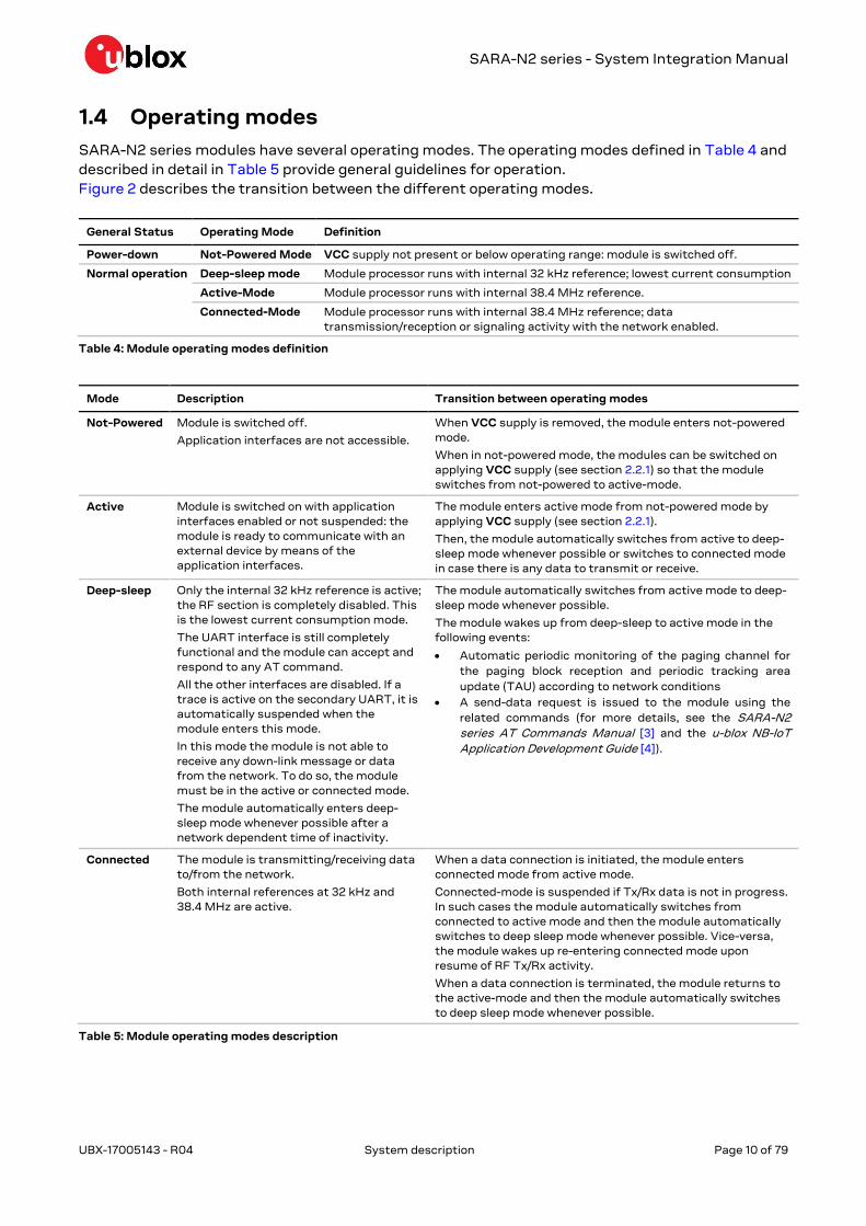
1.4 Operating modes
SARA-N2 series modules have several operating modes. The operating modes defined in Table 4 and
described in detail in Table 5 provide general guidelines for operation.
Figure 2 describes the transition between the different operating modes.
General Status Operating Mode Definition
Power-down Not-Powered Mode VCC supply not present or below operating range: module is switched off.
Normal operation Deep-sleep mode Module processor runs with internal 32 kHz reference; lowest current consumption
Active-Mode Module processor runs with internal 38.4 MHz reference.
Connected-Mode Module processor runs with internal 38.4 MHz reference; data
transmission/reception or signaling activity with the network enabled.
Table 4: Module operating modes definition
Mode Description Transition between operating modes
Not-Powered Module is switched off.
Application interfaces are not accessible.
When VCC supply is removed, the module enters not-powered
mode.
When in not-powered mode, the modules can be switched on
applying VCC supply (see section 2.2.1) so that the module
switches from not-powered to active-mode.
Active Module is switched on with application
interfaces enabled or not suspended: the
module is ready to communicate with an
external device by means of the
application interfaces.
The module enters active mode from not-powered mode by
applying VCC supply (see section 2.2.1).
Then, the module automatically switches from active to deep-
sleep mode whenever possible or switches to connected mode
in case there is any data to transmit or receive.
Deep-sleep Only the internal 32 kHz reference is active;
the RF section is completely disabled. This
is the lowest current consumption mode.
The UART interface is still completely
functional and the module can accept and
respond to any AT command.
All the other interfaces are disabled. If a
trace is active on the secondary UART, it is
automatically suspended when the
module enters this mode.
In this mode the module is not able to
receive any down-link message or data
from the network. To do so, the module
must be in the active or connected mode.
The module automatically enters deep-
sleep mode whenever possible after a
network dependent time of inactivity.
The module automatically switches from active mode to deep-
sleep mode whenever possible.
The module wakes up from deep-sleep to active mode in the
following events:
Automatic periodic monitoring of the paging channel for
the paging block reception and periodic tracking area
update (TAU) according to network conditions
A send-data request is issued to the module using the
related commands (for more details, see the SARA-N2
series AT Commands Manual [3] and the u-blox NB-IoT
Application Development Guide [4]).
Connected The module is transmitting/receiving data
to/from the network.
Both internal references at 32 kHz and
38.4 MHz are active.
When a data connection is initiated, the module enters
connected mode from active mode.
Connected-mode is suspended if Tx/Rx data is not in progress.
In such cases the module automatically switches from
connected to active mode and then the module automatically
switches to deep sleep mode whenever possible. Vice-versa,
the module wakes up re-entering connected mode upon
resume of RF Tx/Rx activity.
When a data connection is terminated, the module returns to
the active-mode and then the module automatically switches
to deep sleep mode whenever possible.
Table 5: Module operating modes description

SARA-N2 series - System Integration Manual
UBX-17005143 - R04 System description Page 11 of 79
Switch ON:• Apply VCC
If there is no activity for a defined time interval
• Network paging• New up-link message request
from the Application Processor
Up-linlk transmission, reception of network signalling indications or downlink data reception
No RF Tx/Rx in progress
Not powered
ActiveConnected Deep-sleep
Switch OFF:• Remove VCC
Figure 2: Operating modes transitions
1.5 Supply interfaces
1.5.1 Module supply input (VCC)
The modules must be supplied via all the three VCC pins that represent the module power supply
input.
The VCC pins are internally connected to the RF power amplifier and to the integrated Power
Management Unit: all supply voltages needed by the module are generated from the VCC supply by
integrated voltage regulators, including V_INT (digital interfaces supply) and VSIM (SIM card
supply).
During operation, the current drawn by the SARA-N2 series modules through the VCC pins can vary
by several orders of magnitude. This ranges from the high peak of current consumption during data
transmission at maximum power level in connected mode, to the low current consumption during
deep-sleep mode (as described in section 1.5.1.2).
1.5.1.1 VCC supply requirements
Table 6 summarizes the requirements for the VCC module supply. See section 2.2.1 for all the
suggestions to properly design a VCC supply circuit compliant to the requirements listed in Table 6.
VCC supply circuit design may affect the RF compliance of the device integrating SARA-N2 series
modules with applicable required certification schemes. Compliance is not guaranteed if the VCC
requirements summarized in the Table 6 are not fulfilled.

SARA-N2 series - System Integration Manual
UBX-17005143 - R04 System description Page 12 of 79
Item Requirement Remark
VCC nominal
voltage
Within VCC normal operating range:
3.1 V min. / 4.0 V max
The module cannot be switched on if VCC voltage
value is below the normal operating range minimum
limit.
Ensure that the input voltage at VCC pins is above
the minimum limit of the normal operating range
for at least more than 3 s after the module
switch-on.
VCC voltage during
normal operation
Within VCC extended operating range:
2.75 V min. / 4.2 V max
The module may switch off when VCC voltage drops
below the extended operating range minimum limit.
Operation above extended operating range limit is
not recommended and may affect device
reliability.
When operating below the normal operating range
minimum limit, the internal PA may not be able to
transmit at the network-required power level.
VCC average
current
Support with margin the highest averaged
VCC current consumption value in connected
mode specified in SARA-N2 series Data Sheet [1].
The maximum average current consumption can be
greater than the specified value according to the
actual antenna mismatching, temperature and
supply voltage.
VCC voltage ripple Noise in the supply has to be minimized High supply voltage ripple values during RF
transmissions in connected-mode directly affect
the RF compliance with applicable certification
schemes.
Table 6: Summary of VCC supply requirements
For the additional specific requirements applicable to the integration of SARA-N211 modules in
devices intended for use in potentially explosive atmospheres, see section 2.11.
1.5.1.2 VCC current consumption profile
Figure 3 shows an example of the module VCC current consumption profile starting from the
switch-on event, followed by different phases and operating modes:
Network registration and context activation procedure
Transmission of an up-link datagram
RRC connection release and related signaling operations
Cyclic paging reception
Deep sleep mode
Timings in the figure are purely indicative since these may significantly change depending on the
network signaling activity. The current consumption peaks occur when the module is in the
connected (transmitting) mode and the value of these peaks is strictly dependent on the
transmitted power, which is regulated by the network. See the electrical specification section in the
SARA-N2 series Data Sheet [1] for more details about the current consumption values in the
different modes and the influence of the transmitting power level.

SARA-N2 series - System Integration Manual
UBX-17005143 - R04 System description Page 13 of 79
A proper power supply circuit for SARA-N2 series modules must be able to withstand the current
values present during the data transmission at maximum power, even though NB-IoT systems
should be designed to keep the module in deep-sleep mode for most of the time, with an extremely
low current consumption in the range of few microamps.
Cu
rre
nt
[mA
]
200
150
100
50
05 10 15 20 25 30 4035 Time [s]
Registration and context activation
RRC connection release (signaling operations)
Up-link data
45 50 6055
Cyclic paging reception Deep Sleep250
65 70 8075 85 90 100950 Figure 3: Example of module current consumption from the switch-on event up to deep-sleep mode
1.5.2 Generic digital interfaces supply output (V_INT)
The same 1.8 V voltage domain used internally to supply the generic digital interfaces (GDI) of
SARA-N2 series modules is also available on the V_INT supply output pin, as described in Figure 4.
The internal regulator that generates the V_INT supply is a low drop out (LDO) converter that is
directly supplied from the VCC main supply input of the module.
The V_INT supply output provides internal short circuit protection to limit start-up current and
protect the load to short circuits.
The V_INT voltage regulator output is disabled (i.e. 0 V) when the module is switched off, while it can
be used to monitor the operating mode when the module is switched on:
When the radio is off, the voltage level is kept low (i.e. 0 V)
When the radio is on, the voltage level is maintained high (i.e. 1.8 V)
Provide a test point connected to the V_INT pin for diagnostic purpose.
Baseband Processor
51VCC
52VCC
53VCC
4V_INT
LDODigital I/O Interfaces
Power Management
SARA-N2 series
Figure 4: SARA-N2 series interfaces supply output (V_INT) simplified block diagram

SARA-N2 series - System Integration Manual
UBX-17005143 - R04 System description Page 14 of 79
1.6 System function interfaces
1.6.1 Module power-on
1.6.1.1 Switch-on events
When the SARA-N2 series modules are in the not-powered mode (i.e. switched off with the VCC
module supply not applied), they can be switched on by:
Rising edge on the VCC supply input to a valid voltage value for module supply, starting from a
voltage value lower than 1.8 V, so that the module switches on applying a proper VCC supply within
the normal operating range. (See SARA-N2 series Data Sheet [1].)
Alternately, the RESET_N pin can be held low during the VCC rising edge, so that the module
switches on by releasing the RESET_N pin when the VCC voltage stabilizes at its nominal value
within the normal range.
1.6.1.2 Switch-on sequence from not-powered mode
Figure 5 shows the modules power-on sequence from the not-powered mode, describing the
following phases:
The external supply is applied to the VCC module supply inputs, representing the start-up event.
The RESET_N line rises suddenly to high logic level due to internal pull-up to VCC.
The V_INT generic digital interfaces supply output is enabled by the integrated power
management unit.
The RXD UART data output pin also rises to the high logic level, at VCC voltage value
A greeting message is sent on the RXD pin (for more details see SARA-N2 series AT Commands
Manual [3]). From now on the module is fully operational and the UART interface is functional
VCC
RESET_N
V_INTHIGH when radio is ON
LOW when radio is OFF
RXD
System State OFF ON
0 s ~3.5 s
Module is
operational
Start-up
event
Greeting text
Figure 5: SARA-N2 series power-on sequence from not-powered mode
No voltage driven by an external application should be applied to the UART interface of the module
before applying the VCC supply, to avoid latch-up of circuits and allow a proper boot of the module.
No voltage driven by an external application should be applied to any generic digital interface of
the module (GPIOs, I2C interface) before the switch-on of the generic digital interface supply
source of the module (V_INT), to avoid latch-up of circuits and allow a proper boot of the module.

SARA-N2 series - System Integration Manual
UBX-17005143 - R04 System description Page 15 of 79
1.6.2 Module power-off
The SARA-N2 series modules can be switched off by:
Removal of the VCC supply supply; the voltage drops below the operating range minimum limit
It is highly recommended to avoid an abrupt removal of the VCC supply during module normal
operation: the VCC supply should be removed only when the V_INT supply output is switched off
by the module.
1.6.3 Module reset
SARA-N2 series modules can be properly reset (rebooted) by:
AT command (see the SARA-N2 series AT Commands Manual [3] for more details).
This command causes an “internal” or “software” reset of the module, which is an asynchronous
reset of the module baseband processor. The current parameter settings are saved in the module’s
non-volatile memory and a proper network detach is performed: this is the proper way to reset the
modules.
An abrupt hardware reset occurs on SARA-N2 series modules when a low level is applied on the
RESET_N input pin for a specific time period. In this case, the current parameter settings are not
saved in the module’s non-volatile memory and a proper network detach is not performed.
As described in Figure 6, the RESET_N input pin is equipped with an internal active pull-up to the
VCC supply.
Baseband Processor
18RESET_N
SARA-N2 series
VCC
Reset
~78 k
Figure 6: SARA-N2 series RESET_N input equivalent circuit description
For more electrical characteristics details see the SARA-N2 series Data Sheet [1].
It is highly recommended to avoid an abrupt hardware reset of the module by forcing a low level on
the RESET_N input pin during module normal operation: the RESET_N line should be set low only
if reset via AT command fails if the module does not provide a reply to a specific AT command after
a time period longer than the one defined in the SARA-N2 series AT Commands Manual [3].
Provide a test point connected to the RESET_N pin for diagnostic purpose.
SARA-N2 series - System Integration Manual
UBX-17005143 - R04 System description Page 16 of 79
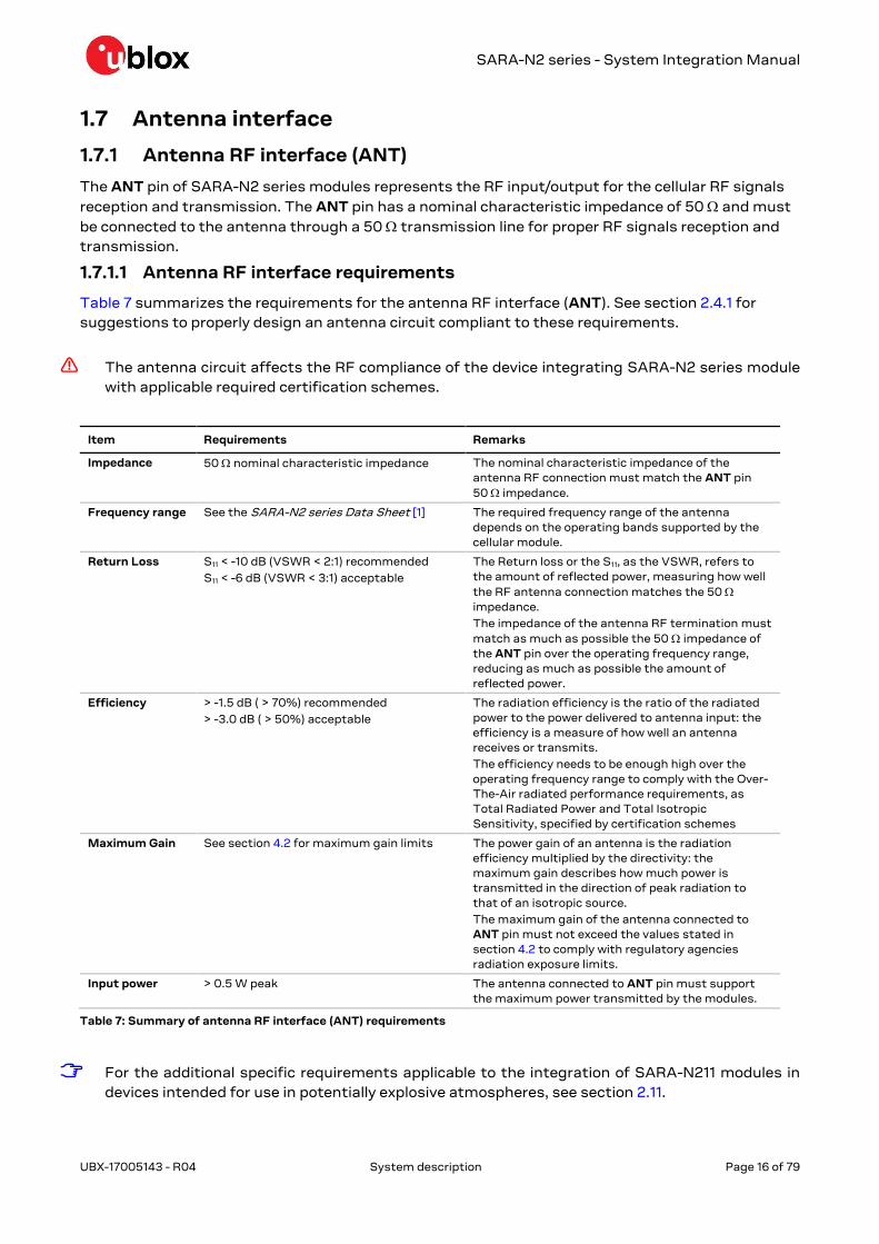
1.7 Antenna interface
1.7.1 Antenna RF interface (ANT)
The ANT pin of SARA-N2 series modules represents the RF input/output for the cellular RF signals
reception and transmission. The ANT pin has a nominal characteristic impedance of 50 and must
be connected to the antenna through a 50 transmission line for proper RF signals reception and
transmission.
1.7.1.1 Antenna RF interface requirements
Table 7 summarizes the requirements for the antenna RF interface (ANT). See section 2.4.1 for
suggestions to properly design an antenna circuit compliant to these requirements.
The antenna circuit affects the RF compliance of the device integrating SARA-N2 series module
with applicable required certification schemes.
Item Requirements Remarks
Impedance 50 nominal characteristic impedance The nominal characteristic impedance of the
antenna RF connection must match the ANT pin
50 impedance.
Frequency range See the SARA-N2 series Data Sheet [1] The required frequency range of the antenna
depends on the operating bands supported by the
cellular module.
Return Loss S11 < -10 dB (VSWR < 2:1) recommended
S11 < -6 dB (VSWR < 3:1) acceptable
The Return loss or the S11, as the VSWR, refers to
the amount of reflected power, measuring how well
the RF antenna connection matches the 50
impedance.
The impedance of the antenna RF termination must
match as much as possible the 50 impedance of
the ANT pin over the operating frequency range,
reducing as much as possible the amount of
reflected power.
Efficiency > -1.5 dB ( > 70%) recommended
> -3.0 dB ( > 50%) acceptable
The radiation efficiency is the ratio of the radiated
power to the power delivered to antenna input: the
efficiency is a measure of how well an antenna
receives or transmits.
The efficiency needs to be enough high over the
operating frequency range to comply with the Over-
The-Air radiated performance requirements, as
Total Radiated Power and Total Isotropic
Sensitivity, specified by certification schemes
Maximum Gain See section 4.2 for maximum gain limits The power gain of an antenna is the radiation
efficiency multiplied by the directivity: the
maximum gain describes how much power is
transmitted in the direction of peak radiation to
that of an isotropic source.
The maximum gain of the antenna connected to
ANT pin must not exceed the values stated in
section 4.2 to comply with regulatory agencies
radiation exposure limits.
Input power > 0.5 W peak The antenna connected to ANT pin must support
the maximum power transmitted by the modules.
Table 7: Summary of antenna RF interface (ANT) requirements
For the additional specific requirements applicable to the integration of SARA-N211 modules in
devices intended for use in potentially explosive atmospheres, see section 2.11.

SARA-N2 series - System Integration Manual
UBX-17005143 - R04 System description Page 17 of 79
1.7.2 Antenna detection interface (ANT_DET)
Antenna detection interface is not supported in the "02" version of the product.
The ANT_DET pin is an Analog to Digital Converter (ADC) input used to sense the antenna presence
evaluating the resistance from the ANT pin to GND by means of an external antenna detection
circuit implemented on the application board. This optional functionality can be managed by
dedicated AT command (for more details see the SARA-N2 series AT Commands Manual [3]).
1.8 SIM interface
SARA-N2 series modules provide a high-speed SIM/ME interface working at 1.8 V, which is available
to connect an external SIM / UICC.
The VSIM supply output provides internal short circuit protection to limit start-up current and
protect the external SIM / UICC to short circuits.
1.9 Serial interfaces
SARA-N2 series modules provide the following serial communication interfaces:
UART interface: 5-wire unbalanced asynchronous serial interface, operating at VCC voltage level
(~3.6 V), supporting (see 1.9.1):
o AT command
o FW upgrades by means of the FOAT feature
o FW upgrades by means of the dedicated tool
Auxiliary UART interface: 2-wire unbalanced asynchronous serial interface, operating at V_INT
level (1.8 V), supporting (see 1.9.2):
o Trace log capture (diagnostic purpose)
DDC interface1: I2C-bus compatible interface, operating at V_INT level (1.8 V), supporting (see
1.9.3):
o Communication with external chips and sensors
o Communication with external u-blox GNSS chips / modules
1.9.1 Asynchronous serial interface (UART)
1.9.1.1 UART features
The UART interface is a 5-wire unbalanced asynchronous serial interface, supporting:
AT command
FW upgrades by means of the FOAT feature
FW upgrades by means of the dedicated tool
The main characteristics of the interface are the following:
Serial port with RS-232 functionality working at the VCC voltage domain (0 V for low data bit or
ON state and ~3.6 V, i.e. VCC, for high data bit or OFF state)
Data lines (RXD as module data output, TXD as module data input)
Hardware flow control lines (CTS as module output, RTS as module input)
Default baud rate: 9600 b/s (4800, 57600 and 115200 b/s baud rates are also supported)
Fixed frame format: 8N1 (8 data bits, No parity, 1 stop bit)
1 Not supported on “02” product version

SARA-N2 series - System Integration Manual
UBX-17005143 - R04 System description Page 18 of 79
The CTS output line can be configured as RING indicator, to signal an incoming message received by
the module or an URC event, or as Network status indicator (for more details see section 1.10 and the
SARA-N2 series AT Commands Manual [3], +URING, +UGPIOC AT commands).
Hardware flow control lines CTS and RTS are not supported by "02" product versions.
The UART interface provides RS-232 functionality conforming to the ITU-T V.24 Recommendation
(more details available in ITU Recommendation [5]): SARA-N2 series modules are designed to
operate as a cellular modem, which represents the Data Circuit-terminating Equipment (DCE)
according to ITU-T V.24 Recommendation [5]. The application processor connected to the module
through the UART interface represents the Data Terminal Equipment (DTE).
The signal names of the SARA-N2 series modules’ UART interface conform to the ITU-T V.24
Recommendation [5]: e.g. the TXD line represents the data transmitted by the DTE (application
processor data line output) and received by the DCE (module data line input).
Figure 7 describes the 8N1 frame format, which is the default configuration with fixed baud rate.
D0 D1 D2 D3 D4 D5 D6 D7
Start of 1-Bytetransfer
Start Bit(Always 0)
Possible Start ofnext transfer
Stop Bit(Always 1)
tbit = 1/(Baudrate)
Normal Transfer, 8N1
Figure 7: Description of UART default frame format (8N1) with fixed baud rate
1.9.1.2 UART signal behavior
At the module switch-on, before the UART interface initialization (as described in the power-on
sequence reported in Figure 5), each pin is first tri-stated and then is set to its related internal reset
state. At the end of the boot sequence, the UART interface is initialized and the UART interface is
enabled as AT commands interface.
The configuration and the behavior of the UART signals after the boot sequence are described
below. See section 1.4 for definition and description of module operating modes referred to in this
section.
RXD signal behavior
The module data output line (RXD) is set by default to the OFF state (high level) at UART
initialization. The greeting message is sent on the RXD line after the completion of the boot
sequence to indicate the completion of the UART interface initialization.
The module holds RXD in the OFF state until the module does not transmit some data.
TXD signal behavior
The module data input line (TXD) is assumed to be controlled by the external host once UART is
initialized.
There is no internal pull-up / pull-down inside the module on the TXD input.

SARA-N2 series - System Integration Manual
UBX-17005143 - R04 System description Page 19 of 79
1.9.1.3 UART and deep sleep mode
To limit the current consumption, SARA-N2 modules automatically enter deep-sleep mode
whenever possible, that is if there is no data to transmit or receive. When in deep-sleep mode the
UART interface is still completely functional and the module can accept and respond to any AT
command. All the other interfaces are disabled.
The application processor should go in standby (or lowest power consumption mode) as soon as the
SARA-N2 module enters the deep-sleep mode and there is no more data to be transmitted.
At any time the DTE can request the module to send data using the related commands (for more
details, see the SARA-N2 series AT Commands Manual [3] and the u-blox NB-IoT Application
Development Guide [4]); these commands automatically force the module to exit the deep-sleep
mode.
1.9.2 Secondary asynchronous serial interface (Secondary UART)
The secondary auxiliary UART interface is a 2-wire unbalanced asynchronous serial interface,
providing:
Trace diagnostic log delivered by the module
The main characteristics of the secondary auxiliary UART interface are:
Serial port with RS-232 functionality working at the V_INT voltage domain (0 V for low data bit or
ON state and 1.8 V, i.e. V_INT, for high data bit or OFF state)
Data line (GPIO1 as module data output)
No flow control
Fixed baud rate: 921600 b/s
Fixed frame format: 8N1 (8 data bits, no parity, 1 stop bit)
Provide a test point connected to the GPIO1 pin for diagnostic purpose.
The trace diagnostic log is temporarily stopped when the module is in deep-sleep mode.
1.9.3 DDC (I2C) interface
DDC (I2C) interface is not supported in the "02" version of the product.
The SDA and SCL pins represent an I2C bus compatible Display Data Channel (DDC) interface,
operating at the V_INT voltage level (1.8 V).

SARA-N2 series - System Integration Manual
UBX-17005143 - R04 System description Page 20 of 79
1.10 General Purpose Input/Output (GPIO)
SARA-N2 series modules provide the following pins:
GPIO1 pin, working at the V_INT (1.8 V) voltage domain, supporting the Secondary UART data
output functionality (see section 1.9.2 and Table 8)
GPIO2 pin, working at the V_INT (1.8 V) voltage domain, not supported by "02" product versions
CTS pin, working at the VCC (3.6 V typical) voltage domain, supporting the Network status
indication and the RING indicator functionality (see section 1.9.1 and Table 8)
For more details about how the pins can be configured, see SARA-N2 series AT Commands
Manual [3], +UGPIOC, +URING AT commands.
Provide a test point connected to the GPIO1 pin for diagnostic purpose.
Function Description Default GPIO Configurable GPIOs
Network status indication Network status: registered home network,
registered roaming, data transmission, no
service
-- CTS
RING indicator Indicates an incoming message received by
the module or an URC event
-- CTS
Secondary UART Secondary UART data output for diagnostic
purpose, to capture diagnostic logs delivered
by the module
GPIO1 GPIO1
Pin disabled Tri-state with an internal active pull-down
enabled
CTS CTS
Table 8: GPIO custom functions configuration
1.11 Reserved pins (RSVD)
SARA-N2 series modules have pins reserved for future use, marked as RSVD.
All the RSVD pins are to be left unconnected on the application board, except for the RSVD pin
number 33 that can be externally connected to ground.

SARA-N2 series - System Integration Manual
UBX-17005143 - R04 Design-in Page 21 of 79
2 Design-in
2.1 Overview
For an optimal integration of SARA-N2 series modules in the final application board, follow the
design guidelines stated in this section.
Every application circuit must be properly designed to guarantee the correct functionality of the
related interface, however a number of points require higher attention during the design of the
application device.
The following list provides a ranking of importance in the application design, starting from the
highest relevance:
1. Module antenna connection: ANT pin. Antenna circuit directly affects the RF compliance of the
device integrating a SARA-N2 series module with the applicable certification schemes. Very
carefully follow the suggestions provided in section 2.4 for schematic and layout design.
2. Module supply: VCC and GND pins. The supply circuit affects the RF compliance of the device
integrating a SARA-N2 series module with applicable certification schemes as well as antenna
circuit design. Very carefully follow the suggestions provided in section 2.2 for schematic and
layout design.
3. SIM interface: VSIM, SIM_CLK, SIM_IO, SIM_RST pins. Accurate design is required to guarantee
SIM card functionality and compliance with applicable conformance standards, reducing also the
risk of RF coupling. Carefully follow the suggestions provided in section 2.5 for schematic and
layout design.
4. System function: RESET_N pin. Accurate design is required to guarantee that the voltage level is
well defined during operation. Carefully follow the suggestions provided in section 2.3 for
schematic and layout design.
5. Other digital interfaces: UART and secondary UART interfaces, DDC I2C-compatible interface and
GPIOs. Accurate design is required to guarantee proper functionality and reduce the risk of digital
data frequency harmonics coupling. Follow the suggestions provided in sections 2.6 and 2.7 for
schematic and layout design.

SARA-N2 series - System Integration Manual
UBX-17005143 - R04 Design-in Page 22 of 79
2.2 Supply interfaces
2.2.1 Module supply (VCC)
2.2.1.1 General guidelines for VCC supply circuit selection and design
All the available VCC pins must be connected to the external supply minimizing the power loss due
to series resistance.
GND pins are internally connected but connect all the available pins to a solid ground on the
application board, since a good (low impedance) connection to external ground can minimize power
loss and improve RF and thermal performance.
SARA-N2 series modules must be supplied through the VCC pins by a proper DC power supply that
should comply with the module VCC requirements summarized in Table 6.
The proper DC power supply can be selected according to the application requirements (see Figure
8) between the different possible supply sources types, which most common ones are the following:
Primary (disposable) battery
Rechargeable Lithium-ion (Li-Ion) or Lithium-ion polymer (Li-Pol) battery
Switching regulator
Low Drop-Out (LDO) linear regulator
Main Supply Available?
BatteryLiSOCl2 3.6 V
Linear LDO Regulator
Main Supply Voltage > 5V?
Switching Step-Down Regulator
No, portable device
No, less than 5 V
Yes, greater than 5 V
Yes, always available
Figure 8: VCC supply concept selection
The NB-IoT technology is primarly intended for battery powered applications. A Lithium Thionyl
Chloride (LiSOCl2) battery directly connected to VCC pins is the usual choice for battery-powered
devices. See sections 2.2.1.2, 2.2.1.3 and 2.2.1.6, 2.2.1.7, 2.2.1.8 for specific design-in.
The DC/DC switching step-down regulator is the typical choice when the available primary supply
source has a nominal voltage much higher (e.g. greater than 5 V) than the modules VCC operating
supply voltage. The use of switching step-down provides the best power efficiency for the overall
application and minimizes current drawn from the main supply source. See sections 2.2.1.2, 2.2.1.4
and 2.2.1.6, 2.2.1.7, 2.2.1.8 for specific design-in.
The use of an LDO linear regulator becomes convenient for a primary supply with a relatively low
voltage (e.g. less than 5 V). In this case the typical 90% efficiency of the switching regulator
diminishes the benefit of voltage step-down and no true advantage is gained in input current
savings. On the opposite side, linear regulators are not recommended for high voltage step-down as
they dissipate a considerable amount of energy in thermal power. See sections 2.2.1.2, 2.2.1.5 and
2.2.1.6, 2.2.1.7, 2.2.1.8 for specific design-in.
The use of rechargeable batteries is not the typical solution for NB-IoT applications, but it is feasible
to implement a suitable external charger circuit. The charger circuit has to be designed to prevent
over-voltage on VCC pins of the module, and it should be selected according to the application
requirements: a DC/DC switching charger is the typical choice when the charging source has an high
nominal voltage (e.g. ~12 V), whereas a linear charger is the typical choice when the charging source
has a relatively low nominal voltage (~5 V). If both a permanent primary supply / charging source (e.g.
~12 V) and a rechargeable back-up battery (e.g. 3.7 V Li-Pol) are simultaneously available in the

SARA-N2 series - System Integration Manual
UBX-17005143 - R04 Design-in Page 23 of 79
application as possible supply sources, then a proper charger / regulator with integrated power path
management function can be selected to supply the module while simultaneously and independently
charging the battery.
The usage of more than one DC supply at the same time should be carefully evaluated: depending on
the supply source characteristics, different DC supply systems can be mutually exclusive.
The usage of supercapacitors on the VCC supply line is generally not recommended since these
components are highly temperature sensitive and may increase current leakages draining the
battery faster.
The following sections highlight some design aspects for power-supply scenarios, providing
application circuit design-in compliant with the module VCC requirements summarized in Table 6.
For the additional specific requirements applicable to the integration of SARA-N211 modules in
devices intended for use in potentially explosive atmospheres, see section 2.11.
2.2.1.2 Guidelines to optimize power consumption
The NB-IoT technology is primarly intended for applications that require small amount of data
exchange per day (i.e. few bytes in uplink and downlink per day) and these are typically battery
powered. Depending on the application type, an operating life of 5 to 15 years is usually required. For
these reasons, the whole application board should be optimized in terms of current consumption
and should carefully take into account the following aspects:
Minimize current leakages on the power supply line
Optimize the antenna matching since an un-matched antenna leads to higher current
consumptions
Use an application processor with UART interface working at the same level of the VCC supply
input of the SARA-N2 module (for example, 3.3 V or 3.6 V). In this way it is possible to avoid voltage
translators on the UART interface, which operates at the VCC voltage level
The application processor should go in standby (or lowest power consumption mode) as soon as
the SARA-N2 module enters the deep-sleep mode and there’s no more data to be transmitted: the
module will automatically enter the deep-sleep mode whenever possible to limit current
consumption and avoid further network registration procedures each time there is an up-link
message to be transmitted.
The application processor can monitor the V_INT level to sense when radio is on or off.
The application processor can detect the presence of down-link messages monitoring the CTS
pin, which provides the Ring Indicator functionality, notifying incoming data received by the
module or an URC event.
Possibility to request new network timers and select the optimum set of values depending on the
intended application use case
2.2.1.3 Guidelines for VCC supply circuit design using a primary battery
The characteristics of a battery connected to VCC pins should meet the following prerequisites to
comply with the module VCC requirements summarized in Table 6:
Maximum pulse and DC discharge current: the non-rechargeable battery with its output circuit
must be capable of delivering to VCC pins the specified average current during a transmission at
maximum power (see the SARA-N2 series Data Sheet [1] for more details). The antenna matching
influences the current consumption; for this reason, the current consumption at maximum Tx
power with the intended antenna (i.e. on the final application board) should be used to characterize
the battery maximum pulse requirements.
The maximum DC discharge current is not always reported in battery data sheets, but it is
typically almost equal to the battery capacity in Amp-hours divided by 1 hour.

SARA-N2 series - System Integration Manual
UBX-17005143 - R04 Design-in Page 24 of 79
DC series resistance: the non-rechargeable battery with its output circuit must be capable to limit
as much as possible the DC resistance provided on the VCC supply line.
The LiSOCl2 (Lithium Thionyl Chloride Batteries) is currently the best technology available for NB-
IoT applications since it provides:
Very low self-discharge behavior and resulting ability to last longer
Highest specific energy per unit weight and energy density per unit volume
Wide operating temperature range
For the selection of the proper battery type, the following parameters should be taken into account:
Capacity: > 3 Ah
Continuous current capability: ~400 mA (the consumption of whole application with the actual
antenna should be considered)
Temperature range: -20 °C to +85 °C
Capacity vs temperature behavior: battery capacity is highly influenced by the temperature. This
must be considered to properly estimate the battery life time
Capacity vs discharge current performance
Voltage vs temperature behavior: the battery voltage typically decreases at low temperatures
values (for example, in the -10 °C / -20 °C range). In all the temperature conditions the battery
voltage must always be above the SARA-N2 minimum extended operating voltage level
Voltage vs pulse duration behavior: this information is typically not provided by battery
manufacturers, and many batteries reach too low voltage values during a long pulse. It is
recommended to execute stress tests on battery samples to verify the voltage behavior as a
function of the pulse duration and to guarantee that the battery voltage is always above the
minimum extended operating voltage level of SARA-N2 series.
Construction technology: spiral wound batteries are generically preferred over the bobbin
construction
o This technology typically supports high current pulses without the need for supercaps
o A bobbin type battery usually does not support the current pulse
Figure 9 shows an example of connection of SARA-N2 module with a primary battery. Table 9 lists
different batty pack part numbers that can be used.
SARA-N2
52 VCC
53 VCC
51 VCC
3V6
C3
Battery pack
C2C1 C4
Figure 9: Suggested schematic design for the VCC voltage supply application circuit using a LiSOCl2 primary battery
SARA-N2 series - System Integration Manual
UBX-17005143 - R04 Design-in Page 25 of 79
Reference Description Part Number - Manufacturer
C1 100 µF Capacitor Tantalum B_SIZE 20% 6.3V 15m T520B107M006ATE015 - Kemet
C2 100 nF Capacitor Ceramic X7R 0402 10% 16 V GRM155R71C104KA01 - Murata
C3 10 nF Capacitor Ceramic X7R 0402 10% 16 V GRM155R71C103KA01 - Murata
C4 56 pF Capacitor Ceramic C0G 0402 5% 25 V GRM1555C1E560JA01 - Murata
Battery pack Size FAT A LiSOCl battery, spiral wound, 3.2Ah ER18505M - Titus Battery
Size C LiSOCl battery, spiral wound, 6.5Ah ER26500M - Titus Battery
Size D LiSOCl battery, spiral wound, 13Ah ER34615M - Titus Battery
Size C LiSOCl battery, spiral wound, 5.8Ah LSH14 – Saft
Size D LiSOCl battery, spiral wound, 13Ah LSH20 - Saft
Table 9: Suggested components for the VCC voltage supply application circuit using a LiSOCl2 primary battery
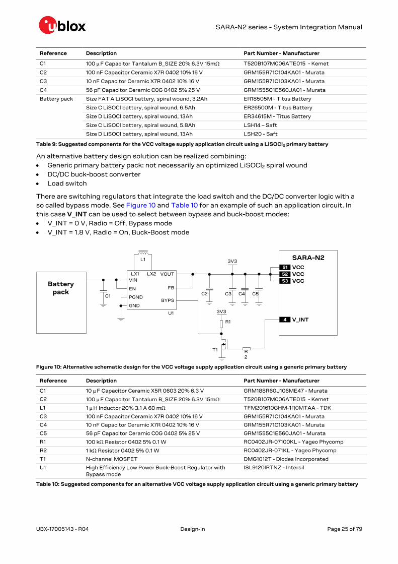
An alternative battery design solution can be realized combining:
Generic primary battery pack: not necessarily an optimized LiSOCl2 spiral wound
DC/DC buck-boost converter
Load switch
There are switching regulators that integrate the load switch and the DC/DC converter logic with a
so called bypass mode. See Figure 10 and Table 10 for an example of such an application circuit. In
this case V_INT can be used to select between bypass and buck-boost modes:
V_INT = 0 V, Radio = Off, Bypass mode
V_INT = 1.8 V, Radio = On, Buck-Boost mode
SARA-N2
52 VCC53 VCC
51 VCC3V3
C3 C5C4C1
LX2
VIN
FB
PGND
VOUT
C2
L1
U1
Battery pack
4 V_INT
BYPS
LX1
EN
GND
T1
3V3
R1
R2
Figure 10: Alternative schematic design for the VCC voltage supply application circuit using a generic primary battery
Reference Description Part Number - Manufacturer
C1 10 µF Capacitor Ceramic X5R 0603 20% 6.3 V GRM188R60J106ME47 - Murata
C2 100 µF Capacitor Tantalum B_SIZE 20% 6.3V 15m T520B107M006ATE015 - Kemet
L1 1 µH Inductor 20% 3.1 A 60 m TFM201610GHM-1R0MTAA - TDK
C3 100 nF Capacitor Ceramic X7R 0402 10% 16 V GRM155R71C104KA01 - Murata
C4 10 nF Capacitor Ceramic X7R 0402 10% 16 V GRM155R71C103KA01 - Murata
C5 56 pF Capacitor Ceramic C0G 0402 5% 25 V GRM1555C1E560JA01 - Murata
R1 100 k Resistor 0402 5% 0.1 W RC0402JR-07100KL - Yageo Phycomp
R2 1 k Resistor 0402 5% 0.1 W RC0402JR-071KL - Yageo Phycomp
T1 N-channel MOSFET DMG1012T - Diodes Incorporated
U1 High Efficiency Low Power Buck-Boost Regulator with
Bypass mode
ISL9120IRTNZ - Intersil
Table 10: Suggested components for an alternative VCC voltage supply application circuit using a generic primary battery

SARA-N2 series - System Integration Manual
UBX-17005143 - R04 Design-in Page 26 of 79
2.2.1.4 Guidelines for VCC supply circuit design using a switching regulator
The use of a switching regulator is suggested when the difference from the available supply rail to
the VCC value is high: switching regulators provide good efficiency transforming a 12 V or greater
voltage supply to the typical 3.6 V value of the VCC supply.
The characteristics of the switching regulator connected to VCC pins should meet the following
prerequisites to comply with the module VCC requirements summarized in Table 6:
Power capability: the switching regulator with its output circuit must be capable of providing a
voltage value to the VCC pins within the specified operating range and must be capable of
delivering to VCC pins the specified average current during a transmission at maximum power
(see SARA-N2 series Data Sheet [1]).
Low output ripple: the switching regulator together with its output circuit must be capable of
providing a clean (low noise) VCC voltage profile.
PWM mode operation: it is preferable to select regulators with Pulse Width Modulation (PWM)
mode. While in connected-mode Pulse Frequency Modulation (PFM) mode and PFM/PWM mode,
transitions must be avoided to reduce the noise on the VCC voltage profile. Switching regulators
that are able to switch between low ripple PWM mode and high efficiency burst or PFM mode can
be used, provided the mode transition occurs when the module changes status from active-mode
to connected-mode: it is suggest to use a regulator that switches from the PWM mode to the
burst or PFM mode at an appropriate current threshold (e.g. 10 mA).
Figure 11 and the components listed in Table 11 show an example of a power supply circuit, where the
module VCC is supplied by a step-down switching regulator capable of delivering the specified
maximum current to the VCC pins, with low output ripple and with fixed switching frequency in
PWM.
12V
R5
C6C1
VCC
INH
FSW
SYNC
OUT
GND
2
6
3 1
7
8
C3
C2
D1R1
R2
L1
U1 FB
COMP
5
4
R3
C4R4
C5
SARA-N2
52 VCC53 VCC
51 VCC
GND
3V6
C7 C8 C9
Figure 11: Suggested schematic design for the VCC voltage supply application circuit using a step-down regulator

SARA-N2 series - System Integration Manual
UBX-17005143 - R04 Design-in Page 27 of 79
Reference Description Part Number - Manufacturer
C1 22 µF Capacitor Ceramic X5R 1210 10% 25 V GRM32ER61E226KE15 - Murata
C2 100 µF Capacitor Tantalum B_SIZE 20% 6.3V 15m T520B107M006ATE015 - Kemet
C3 5.6 nF Capacitor Ceramic X7R 0402 10% 50 V GRM155R71H562KA88 - Murata
C4 6.8 nF Capacitor Ceramic X7R 0402 10% 50 V GRM155R71H682KA88 - Murata
C5 56 pF Capacitor Ceramic C0G 0402 5% 50 V GRM1555C1H560JA01 - Murata
C6 220 nF Capacitor Ceramic X7R 0603 10% 25 V GRM188R71E224KA88 - Murata
C7 100 nF Capacitor Ceramic X7R 0402 10% 16 V GRM155R71C104KA01 - Murata
C8 10 nF Capacitor Ceramic X7R 0402 10% 16 V GRM155R71C103KA01 - Murata
C9 56 pF Capacitor Ceramic C0G 0402 5% 25 V GRM1555C1E560JA01 - Murata
D1 Schottky Diode 25V 2 A STPS2L25 - STMicroelectronics
L1 5.2 µH Inductor 30% 5.28A 22 m MSS1038-522NL - Coilcraft
R1 4.7 k Resistor 0402 1% 0.063 W RC0402FR-074K7L - Yageo
R2 1 k Resistor 0402 1% 0.063 W RC0402FR-071KL - Yageo
R3 82 Resistor 0402 5% 0.063 W RC0402JR-0782RL - Yageo
R4 8.2 k Resistor 0402 5% 0.063 W RC0402JR-078K2L - Yageo
R5 39 k Resistor 0402 5% 0.063 W RC0402JR-0739KL - Yageo
U1 Step-Down Regulator 8-VFQFPN 0.7 A 1 MHz L5980TR - ST Microelectronics
Table 11: Suggested components for the VCC voltage supply application circuit using a step-down regulator

SARA-N2 series - System Integration Manual
UBX-17005143 - R04 Design-in Page 28 of 79
2.2.1.5 Guidelines for VCC supply circuit design using an LDO linear regulator
The use of a linear regulator is suggested when the difference from the available supply rail and the
VCC value is low: linear regulators provide high efficiency when transforming a 5 V supply to a
voltage value within the module VCC normal operating range.
The characteristics of the LDO linear regulator connected to the VCC pins should meet the following
prerequisites to comply with the module VCC requirements summarized in Table 6:
Power capabilities: the LDO linear regulator with its output circuit must be capable of providing a
proper voltage value to the VCC pins and of delivering to VCC pins the specified maximum average
current during a transmission at maximum power (see the SARA-N2 series Data Sheet [1])
Power dissipation: the power handling capability of the LDO linear regulator must be checked to
limit its junction temperature to the maximum rated operating range (i.e. check the voltage drop
from the max input voltage to the min output voltage to evaluate the power dissipation of the
regulator)
Figure 12 and the components listed in Table 12 show a power supply circuit example, where the VCC
module supply is provided by an LDO linear regulator capable of delivering the specified current.
It is recommended to configure the LDO linear regulator to generate a voltage supply value slightly
below the maximum limit of the module VCC normal operating range. This reduces the power on the
linear regulator and improves the whole thermal design of the supply circuit.
5V
C1
IN OUT
ADJ
GND
1
2 4
5
3
C2R1
R2
U1
EN
SARA-N2
52 VCC
53 VCC
51 VCC
GND
3V6
C3 C4 C5
Figure 12: Suggested schematic design for the VCC voltage supply application circuit using an LDO linear regulator
Reference Description Part Number - Manufacturer
C1 10 µF Capacitor Ceramic X5R 0603 20% 6.3 V GRM188R60J106ME47 - Murata
C2 100 µF Capacitor Tantalum B_SIZE 20% 6.3V 15m T520B107M006ATE015 - Kemet
R1 29.4 k Resistor 0402 5% 0.1 W RC0402FR-0729K4L - Yageo Phycomp
R2 4.7 k Resistor 0402 5% 0.1 W RC0402JR-074K7L - Yageo Phycomp
U1 LDO Linear Regulator ADJ 800 mA LP38511TJ-ADJ/NOPB - Texas Instrument
C3 100 nF Capacitor Ceramic X7R 0402 10% 16 V GRM155R71C104KA01 - Murata
C4 10 nF Capacitor Ceramic X7R 0402 10% 16 V GRM155R71C103KA01 - Murata
C5 56 pF Capacitor Ceramic C0G 0402 5% 25 V GRM1555C1E560JA01 - Murata
Table 12: Suggested components for VCC voltage supply application circuit using an LDO linear regulator
SARA-N2 series - System Integration Manual
UBX-17005143 - R04 Design-in Page 29 of 79
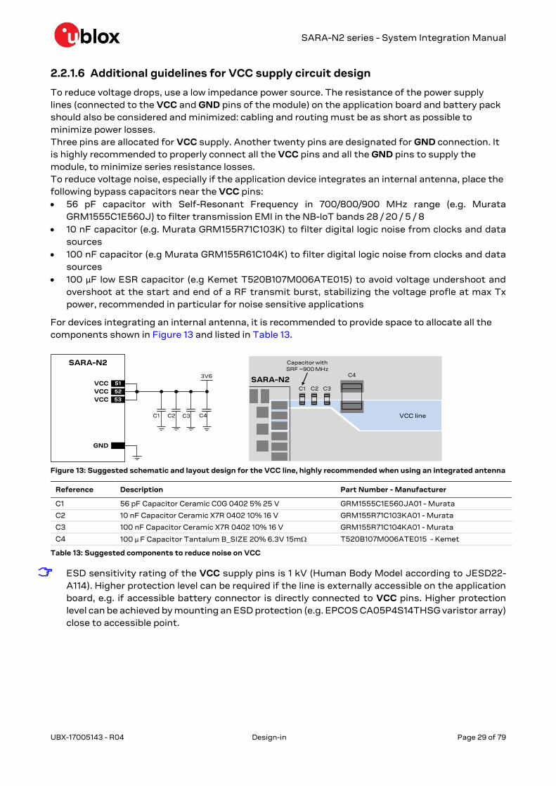
2.2.1.6 Additional guidelines for VCC supply circuit design
To reduce voltage drops, use a low impedance power source. The resistance of the power supply
lines (connected to the VCC and GND pins of the module) on the application board and battery pack
should also be considered and minimized: cabling and routing must be as short as possible to
minimize power losses.
Three pins are allocated for VCC supply. Another twenty pins are designated for GND connection. It
is highly recommended to properly connect all the VCC pins and all the GND pins to supply the
module, to minimize series resistance losses.
To reduce voltage noise, especially if the application device integrates an internal antenna, place the
following bypass capacitors near the VCC pins:
56 pF capacitor with Self-Resonant Frequency in 700/800/900 MHz range (e.g. Murata
GRM1555C1E560J) to filter transmission EMI in the NB-IoT bands 28 / 20 / 5 / 8
10 nF capacitor (e.g. Murata GRM155R71C103K) to filter digital logic noise from clocks and data
sources
100 nF capacitor (e.g Murata GRM155R61C104K) to filter digital logic noise from clocks and data
sources
100 µF low ESR capacitor (e.g Kemet T520B107M006ATE015) to avoid voltage undershoot and
overshoot at the start and end of a RF transmit burst, stabilizing the voltage profle at max Tx
power, recommended in particular for noise sensitive applications
For devices integrating an internal antenna, it is recommended to provide space to allocate all the
components shown in Figure 13 and listed in Table 13.
C1
GND
C2
SARA-N2
52VCC
53VCC
51VCC3V6
C4 VCC line
Capacitor with SRF ~900 MHz
C1 C3C2
C3
C4SARA-N2
Figure 13: Suggested schematic and layout design for the VCC line, highly recommended when using an integrated antenna
Reference Description Part Number - Manufacturer
C1 56 pF Capacitor Ceramic C0G 0402 5% 25 V GRM1555C1E560JA01 - Murata
C2 10 nF Capacitor Ceramic X7R 0402 10% 16 V GRM155R71C103KA01 - Murata
C3 100 nF Capacitor Ceramic X7R 0402 10% 16 V GRM155R71C104KA01 - Murata
C4 100 µF Capacitor Tantalum B_SIZE 20% 6.3V 15m T520B107M006ATE015 - Kemet
Table 13: Suggested components to reduce noise on VCC
ESD sensitivity rating of the VCC supply pins is 1 kV (Human Body Model according to JESD22-
A114). Higher protection level can be required if the line is externally accessible on the application
board, e.g. if accessible battery connector is directly connected to VCC pins. Higher protection
level can be achieved by mounting an ESD protection (e.g. EPCOS CA05P4S14THSG varistor array)
close to accessible point.

SARA-N2 series - System Integration Manual
UBX-17005143 - R04 Design-in Page 30 of 79
2.2.1.7 Guidelines for VCC supply layout design
Good connection of the module VCC pins with DC supply source is required for correct RF
performance. Guidelines are summarized in the following list:
All the available VCC pins must be connected to the DC source.
VCC connection must be as wide as possible and as short as possible.
Any series component with Equivalent Series Resistance (ESR) greater than few milliohms must
be avoided.
VCC connection must be routed through a PCB area separated from sensitive analog signals and
sensitive functional units: it is good practice to interpose at least one layer of PCB ground between
VCC track and other signal routing.
The bypass capacitors in the pF range described in Figure 13 and Table 13 should be placed as close
as possible to the VCC pins. This is highly recommended if the application device integrates an
internal antenna.
High frequency voltage ripples on the VCC line may result in unwanted spurious modulation of
transmitter RF signal. This is more likely to happen with switching DC-DC converters, in which
case it is better to select the highest operating frequency for the switcher and add a large L-C filter
before connecting to the SARA-N2 series modules in the worst case.
If VCC is protected by transient voltage suppressor to ensure that the voltage maximum ratings
are not exceeded, place the protecting device along the path from the DC source toward the
cellular module, preferably closer to the DC source (otherwise protection functionality may be
compromised).
2.2.1.8 Guidelines for grounding layout design
Good connection of the module GND pins with application board solid ground layer is required for
correct RF performance. It significantly reduces EMC issues and provides a thermal heat sink for the
module.
Connect each GND pin with application board solid GND layer. It is strongly recommended that
each GND pin surrounding VCC pins have one or more dedicated via down to the application board
solid ground layer.
The VCC supply current flows back to main DC source through GND as ground current: provide
adequate return path with suitable uninterrupted ground plane to main DC source.
It is recommended to implement one layer of the application board as ground plane as wide as
possible.
If the application board is a multilayer PCB, then all the board layers should be filled with GND plane
as much as possible and each GND area should be connected together with complete via stack
down to the main ground layer of the board.
If the whole application device is composed by more than one PCB, then it is required to provide a
good and solid ground connection between the GND areas of all the different PCBs.
Good grounding of GND pins also ensures thermal heat sink. This is critical during call connection,
when the real network commands the module to transmit at maximum power: proper grounding
helps prevent module overheating.

SARA-N2 series - System Integration Manual
UBX-17005143 - R04 Design-in Page 31 of 79
2.2.2 Interface supply (V_INT)
2.2.2.1 Guidelines for V_INT circuit design
The V_INT digital interfaces 1.8 V supply output can be mainly used to:
Indicate when the module is switched on, and radio is on (see section 1.6.1 for more details)
Do not apply loads that might exceed the limit for maximum available current from V_INT supply,
as this can cause malfunctions in internal circuitry supplies to the same domain. The SARA-N2
series Data Sheet [1] describes the detailed electrical characteristics.
V_INT can only be used as an output; do not connect any external regulator on V_INT.
V_INT supply output pin provides internal short circuit protection to limit start-up current and
protect the device in short circuit situations. No additional external short circuit protection is
required.
ESD sensitivity rating of the V_INT supply pin is 1 kV (Human Body Model according to JESD22-
A114). Higher protection level could be required if the line is externally accessible on the application
board. Higher protection level can be achieved by mounting an ESD protection (e.g. EPCOS
CA05P4S14THSG varistor array) close to accessible point.
It is recommended providing direct access to the V_INT supply output pin on the application board
by means of testpoint directly accessible for diagnostic purpose
2.2.2.2 Guidelines for V_INT layout design
There are no specific layout design recommendations for V_INT output.

SARA-N2 series - System Integration Manual
UBX-17005143 - R04 Design-in Page 32 of 79
2.3 System functions interfaces
2.3.1 Module reset (RESET_N)
2.3.1.1 Guidelines for RESET_N circuit design
As described in SARA-N2 series Data Sheet [1], the module has an internal pull-up resistor on the
reset input line, so an external pull-up is not required on the application board.
When the RESET_N input is connected to a push button that shorts the RESET_N pin to ground, the
pin will be externally accessible on the application device. According to EMC/ESD requirements of
the application, provide an additional ESD protection (e.g. EPCOS CA05P4S14THSG varistor array)
on the line connected to this pin, close to accessible point, as described in Figure 14 and Table 14.
ESD sensitivity rating of the RESET_N pin is 1 kV (Human Body Model according to JESD22-A114).
Higher protection level can be required if the line is externally accessible on the application board,
e.g. if an accessible push button is directly connected to RESET_N pin. Higher protection level can
be achieved by mounting an ESD protection (e.g. EPCOS CA05P4S14THSG varistor array) close to
accessible point.
When the RESET_N input is connected to an external device (e.g. application processor), an open
drain output can be directly connected without any external pull-up, as described in Figure 14 and
Table 14. The internal pull-up resistor provided by the module pulls the line to the high logic level
when the application processor does not force the RESET_N pin low. A compatible push-pull output
of an application processor can be used too.
1:1 scaling
SARA-N2 series
18 RESET_N
Reset push button
ESD
Open Drain Output
Application Processor SARA-N2 series
18 RESET_NTP TP
~78k
VCC
~78k
VCC
Figure 14: RESET_N application circuits using a push button and an open drain output of an application processor
Reference Description Remarks
ESD Varistor for ESD protection CT0402S14AHSG - EPCOS
Table 14: Example of ESD protection component for the RESET_N application circuit
If the external reset function is not required by the customer application, the RESET_N input pin
can be left unconnected to external components, but it is recommended providing direct access
on the application board by means of accessible testpoint for diagnostic purpose.
2.3.1.2 Guidelines for RESET_N layout design
The reset circuit (RESET_N) requires careful layout due to the pin function: ensure that the voltage
level is well defined during operation and no transient noise is coupled on this line, otherwise the
module might detect a spurious reset request. It is recommended to keep the connection line to
RESET_N as short as possible.

SARA-N2 series - System Integration Manual
UBX-17005143 - R04 Design-in Page 33 of 79
2.4 Antenna interface
The ANT pin, provided by all the SARA-N2 series modules, represents the RF input/output used to
transmit and receive the RF cellular signals: the antenna must be connected to this pin. The ANT pin
has a nominal characteristic impedance of 50 and must be connected to the antenna through a 50
transmission line to allow transmission and reception of radio frequency (RF) signals in the
operating bands.
2.4.1 Antenna RF interface (ANT)
2.4.1.1 General guidelines for antenna selection and design
The cellular antenna is the most critical component to be evaluated: care must be taken about it at
the start of the design development, when the physical dimensions of the application board are
under analysis/decision, since the RF compliance of the device integrating a SARA-N2 series module
with all the applicable required certification schemes depends from antenna radiating performance.
Cellular antennas are typically available as:
External antenna (e.g. linear monopole):
o External antenna usage basically does not imply physical restrictions on the design of the PCB
where the SARA-N2 series module is mounted.
o The radiation performance mainly depends on the antenna: select the antenna with optimal
radiating performance in the operating bands.
o If antenna detection functionality is required, select an antenna assembly provided with a
proper built-in diagnostic circuit with a resistor connected to ground: see section 2.4.2.
o Select an RF cable with minimum insertion loss: additional insertion loss due to low quality or
long cable reduces radiation performance.
o Select a suitable 50 connector providing proper PCB-to-RF-cable transition: it is
recommended to strictly follow the layout and cable termination guidelines provided by the
connector manufacturer.
Integrated antenna (PCB antennas such as patches or ceramic SMT elements):
o Internal integrated antenna implies physical restriction to the design of the PCB: the ground
plane can be reduced down to a minimum size that must be similar to the quarter of the
wavelength of the minimum frequency that has to be radiated. As numerical example:
Frequency = 750 MHz Wavelength = 40 cm Minimum GND plane size = 10 cm
o The radiation performance depends on the whole PCB and antenna system design, including
product mechanical design and usage: select the antenna with optimal radiating performance
in the operating bands according to the mechanical specifications of the PCB and the whole
product.
o Select a complete custom antenna designed by an antenna manufacturer if the required
ground plane dimensions are very small (e.g. less than 6.5 cm long and 4 cm wide): the antenna
design process should begin at the start of the whole product design process.
o Select an integrated antenna solution provided by an antenna manufacturer if the required
ground plane dimensions are large enough according to the related integrated antenna
solution specifications: the antenna selection and the definition of its placement in the product
layout should begin at the start of the product design process.
o It is highly recommended to strictly follow the detailed and specific guidelines provided by the
antenna manufacturer regarding correct installation and deployment of the antenna system,
including PCB layout and matching circuitry.
o Further to the custom PCB and product restrictions, the antenna may require tuning to obtain
the required performance to comply with applicable certification schemes. It is recommended
to ask the antenna manufacturer for design-in guidelines related to the custom application.

SARA-N2 series - System Integration Manual
UBX-17005143 - R04 Design-in Page 34 of 79
In both cases, selecting an external or an internal antenna, observe these recommendations:
Select an antenna providing optimal return loss (or V.S.W.R.) figure over all the operating
frequencies.
Select an antenna providing optimal efficiency figure over all the operating frequencies.
Select an antenna providing appropriate gain figure (i.e. combined antenna directivity and
efficiency figure) so that the electromagnetic field radiation intensity do not exceed the regulatory
limits specified in some countries (e.g. by FCC in the United States).
For the additional specific guidelines for SARA-N211 modules integration in applications intended
for use in potentially explosive atmospheres, see section 2.11.
2.4.1.2 Guidelines for antenna RF interface design
Guidelines for ANT pin RF connection design
Proper transition between the ANT pin and the application board PCB must be provided,
implementing the following design-in guidelines for the layout of the application PCB close to the
pad designed for the ANT pin:
On a multi layer board, the whole layer stack below the RF connection should be free of digital lines
Increase GND keep-out (i.e. clearance, a void area) around the ANT pad, on the top layer of the
application PCB, to at least 250 µm up to adjacent pads metal definition and up to 400 µm on the
area below the module, to reduce parasitic capacitance to ground, as described in the left picture
in Figure 15
Add GND keep-out (i.e. clearance, a void area) on the buried metal layer below the ANT pad if the
top-layer to buried layer dielectric thickness is below 200 µm, to reduce parasitic capacitance to
ground, as described in the right picture in Figure 15
Min. 250 µm
Min. 400 µmGNDANT
GND clearance on very close buried layer
below ANT pad
GND clearance on top layer
around ANT pad
Figure 15: GND keep-out area on the top layer around ANT pad and on the very close buried layer below ANT pad
Guidelines for RF transmission line design
The transmission line from the ANT pad up to antenna connector or up to the internal antenna pad
must be designed so that the characteristic impedance is as close as possible to 50 .
The transmission line can be designed as a micro strip (consists of a conducting strip separated
from a ground plane by a dielectric material) or a strip line (consists of a flat strip of metal which is
sandwiched between two parallel ground planes within a dielectric material). The micro strip,
implemented as a coplanar waveguide, is the most common configuration for printed circuit board.

SARA-N2 series - System Integration Manual
UBX-17005143 - R04 Design-in Page 35 of 79
Figure 16 and Figure 17 provide two examples of proper 50 coplanar waveguide designs. The first
transmission line can be implemented in case of 4-layer PCB stack-up herein described, the second
transmission line can be implemented in case of 2-layer PCB stack-up herein described.
35 µm
35 µm
35 µm
35 µm
270 µm
270 µm
760 µm
L1 Copper
L3 Copper
L2 Copper
L4 Copper
FR-4 dielectric
FR-4 dielectric
FR-4 dielectric
380 µm 500 µm500 µm
Figure 16: Example of 50 coplanar waveguide transmission line design for the described 4-layer board layup
35 µm
35 µm
1510 µm
L2 Copper
L1 Copper
FR-4 dielectric
1200 µm 400 µm400 µm
Figure 17: Example of 50 coplanar waveguide transmission line design for the described 2-layer board layup
If the two examples do not match the application PCB layup, the 50 characteristic impedance
calculation can be made using the HFSS commercial finite element method solver for
electromagnetic structures from Ansys Corporation, or using freeware tools like AppCAD from
Agilent (www.agilent.com) or TXLine from Applied Wave Research (www.mwoffice.com), taking care
of the approximation formulas used by the tools for the impedance computation.
To achieve a 50 characteristic impedance, the width of the transmission line must be chosen
depending on:
the thickness of the transmission line itself (e.g. 35 µm in the example of Figure 16 and Figure 17)
the thickness of the dielectric material between the top layer (where the transmission line is
routed) and the inner closer layer implementing the ground plane (e.g. 270 µm in Figure 16, 1510 µm
in Figure 17)
the dielectric constant of the dielectric material (e.g. dielectric constant of the FR-4 dielectric
material in Figure 16 and Figure 17)
the gap from the transmission line to the adjacent ground plane on the same layer of the
transmission line (e.g. 500 µm in Figure 16, 400 µm in Figure 17)
If the distance between the transmission line and the adjacent GND area (on the same layer) does
not exceed 5 times the track width of the micro strip, use the “Coplanar Waveguide” model for the
50 calculation.
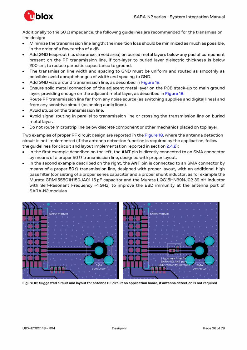
SARA-N2 series - System Integration Manual
UBX-17005143 - R04 Design-in Page 36 of 79
Additionally to the 50 impedance, the following guidelines are recommended for the transmission
line design:
Minimize the transmission line length: the insertion loss should be minimized as much as possible,
in the order of a few tenths of a dB.
Add GND keep-out (i.e. clearance, a void area) on buried metal layers below any pad of component
present on the RF transmission line, if top-layer to buried layer dielectric thickness is below
200 µm, to reduce parasitic capacitance to ground.
The transmission line width and spacing to GND must be uniform and routed as smoothly as
possible: avoid abrupt changes of width and spacing to GND.
Add GND vias around transmission line, as described in Figure 18.
Ensure solid metal connection of the adjacent metal layer on the PCB stack-up to main ground
layer, providing enough on the adjacent metal layer, as described in Figure 18.
Route RF transmission line far from any noise source (as switching supplies and digital lines) and
from any sensitive circuit (as analog audio lines).
Avoid stubs on the transmission line.
Avoid signal routing in parallel to transmission line or crossing the transmission line on buried
metal layer.
Do not route microstrip line below discrete component or other mechanics placed on top layer.
Two examples of proper RF circuit design are reported in the Figure 18, where the antenna detection
circuit is not implemented (if the antenna detection function is required by the application, follow
the guidelines for circuit and layout implementation reported in section 2.4.2):
In the first example described on the left, the ANT pin is directly connected to an SMA connector
by means of a proper 50 transmission line, designed with proper layout.
In the second example described on the right, the ANT pin is connected to an SMA connector by
means of a proper 50 transmission line, designed with proper layout, with an additional high
pass filter (consisting of a proper series capacitor and a proper shunt inductor, as for example the
Murata GRM1555C1H150JA01 15 pF capacitor and the Murata LQG15HN39NJ02 39 nH inductor
with Self-Resonant Frequency ~1 GHz) to improve the ESD immunity at the antenna port of
SARA-N2 modules
SARA module
SMAconnector
SARA module
SMAconnector
High-pass filter for SARA-N2 ANT port
ESD immunity increase
Figure 18: Suggested circuit and layout for antenna RF circuit on application board, if antenna detection is not required

SARA-N2 series - System Integration Manual
UBX-17005143 - R04 Design-in Page 37 of 79
Guidelines for RF termination design
The RF termination must provide a characteristic impedance of 50 as well as the RF transmission
line up to the RF termination itself, to match the characteristic impedance of the ANT pin of the
module.
However, real antennas do not have perfect 50 load on all the supported frequency bands.
Therefore, to reduce as much as possible performance degradation due to antenna mismatch, the
RF termination must provide optimal return loss (or V.S.W.R.) figure over all the operating
frequencies, as summarized in Table 7.
If an external antenna is used, the antenna connector represents the RF termination on the PCB:
Use a suitable 50 connector providing proper PCB-to-RF-cable transition.
Strictly follow the connector manufacturer’s recommended layout, for example:
o SMA Pin-Through-Hole connectors require GND keep-out (i.e. clearance, a void area) on all the
layers around the central pin up to annular pads of the four GND posts, as shown in Figure 18.
o U.FL surface mounted connectors require no conductive traces (i.e. clearance, a void area) in
the area below the connector between the GND land pads.
Cut out the GND layer under RF connectors and close to buried vias, to remove stray capacitance
and thus keep the RF line 50 : e.g. the active pad of U.FL connectors needs to have a GND keep-
out (i.e. clearance, a void area) at least on first inner layer to reduce parasitic capacitance to ground
If an integrated antenna is used, the RF termination is represented by the integrated antenna itself:
Use an antenna designed by an antenna manufacturer, providing the best possible return loss (or
V.S.W.R.).
Provide a ground plane large enough according to the related integrated antenna requirements:
the ground plane of the application PCB can be reduced to a minimum size that must be similar to
one quarter of wavelength of the minimum frequency that has to be radiated. As numerical
example:
Frequency = 750 MHz Wavelength = 40 cm Minimum GND plane size = 10 cm
It is highly recommended to strictly follow the detailed and specific guidelines provided by the
antenna manufacturer regarding correct installation and deployment of the antenna system,
including PCB layout and matching circuitry.
Further to the custom PCB and product restrictions, the antenna may require a tuning to comply
with all the applicable required certification schemes. It is recommended to consult the antenna
manufacturer for the design-in guidelines for the antenna related to the custom application.
Additionally, these recommendations regarding the antenna system must be followed:
Do not include antenna within closed metal case.
Do not place the antenna in close vicinity to end users, since the emitted radiation in human tissue
is limited by regulatory requirements.
Place the antenna far from sensitive analog systems or employ countermeasures to reduce
electromagnetic compatibility issues.
Take care of interaction between co-located RF systems since the cellular transmitted RF power
may interact or disturb the performance of companion systems.
The antenna shall provide optimal efficiency figure over all the operating frequencies.
The antenna shall provide appropriate gain figure (i.e. combined antenna directivity and efficiency
figure) so that the electromagnetic field radiation intensity does not exceed the regulatory limits
specified in some countries (e.g. by FCC in the United States).
Consider including extra footprints for a “pi” network in between the cellular module and the
antenna, for further improvement in the antenna matching circuit to reach optimal antenna
performance.

SARA-N2 series - System Integration Manual
UBX-17005143 - R04 Design-in Page 38 of 79
Examples of antennas
Table 15 lists some examples of possible internal on-board surface-mount antennas
Manufacturer Part Number Product Name Description
Taoglas PA.710.A Warrior GSM / WCDMA / LTE SMD Antenna
698..960 MHz, 1710..2170 MHz, 2300..2400 MHz, 2490..2690 MHz
40.0 x 6.0 x 5.0 mm
Taoglas PCS.06.A Havok GSM / WCDMA / LTE SMD Antenna
698..960 MHz, 1710..2170 MHz, 2500..2690 MHz
42.0 x 10.0 x 3.0 mm
Taoglas MCS6.A GSM / WCDMA / LTE SMD Antenna
698..960 MHz, 1710..2690 MHz
42.0 x 10.0 x 3.0 mm
Antenova SR4L002 Lucida GSM / WCDMA / LTE SMD Antenna
698..960 MHz, 1710..2170 MHz, 2300..2400 MHz, 2490..2690 MHz
35.0 x 8.5 x 3.2 mm
Ethertronics P822601 GSM / WCDMA / LTE SMD Antenna
698..960 MHz, 1710..2170 MHz, 2490..2700 MHz
50.0 x 8.0 x 3.2 mm
Ethertronics P822602 GSM / WCDMA / LTE SMD Antenna
698..960 MHz, 1710..2170 MHz, 2490..2700 MHz
50.0 x 8.0 x 3.2 mm
Ethertronics 1002436 GSM / WCDMA / LTE Vertical Mount Antenna
698..960 MHz, 1710..2700 MHz
50.6 x 19.6 x 1.6 mm
Pulse W3796 Domino GSM / WCDMA / LTE SMD Antenna
698..960 MHz, 1427..1661 MHz, 1695..2200 MHz, 2300..2700 MHz
42.0 x 10.0 x 3.0 mm
TE Connectivity 2118310-1 GSM / WCDMA / LTE Vertical Mount Antenna
698..960 MHz, 1710..2170 MHz, 2300..2700 MHz
74.0 x 10.6 x 1.6 mm
Molex 1462000001 GSM / WCDMA / LTE SMD Antenna
698..960 MHz, 1700..2700 MHz
40.0 x 5.0 x 5.0 mm
Cirocomm DPAN0S07 GSM / WCDMA / LTE SMD Antenna
698..960 MHz, 1710..2170 MHz, 2500..2700 MHz
37.0 x 5.0 x 5.0 mm
Table 15: Examples of internal surface-mount antennas

SARA-N2 series - System Integration Manual
UBX-17005143 - R04 Design-in Page 39 of 79
Table 16 lists some examples of possible internal off-board PCB-type antennas with cable and
connector.
Manufacturer Part Number Product Name Description
Taoglas FXUB63.07.0150C GSM / WCDMA / LTE PCB Antenna with cable and U.FL connector
698..960 MHz, 1575.42 MHz, 1710..2170 MHz, 2400..2690 MHz
96.0 x 21.0 mm
Taoglas FXUB66.07.0150C Maximus GSM / WCDMA / LTE Antenna on flexible PCB with cable and U.FL
698..960 MHz, 1390..1435 MHz, 1575.42 MHz, 1710..2170 MHz,
2400..2700 MHz, 3400..3600 MHz, 4800..6000 MHz
120.2 x 50.4 mm
Antenova SRFL029 Moseni GSM / WCDMA / LTE Antenna on flexible PCB with cable and U.FL
689..960 MHz, 1710..2170 MHz, 2300..2400 MHz, 2500..2690 MHz
110.0 x 20.0 mm
Antenova SRFL026 Mitis GSM / WCDMA / LTE Antenna on flexible PCB with cable and U.FL
689..960 MHz, 1710..2170 MHz, 2300..2400 MHz, 2500..2690 MHz
110.0 x 20.0 mm
Ethertronics 1002289 GSM / WCDMA / LTE Antenna on flexible PCB with cable and U.FL
698..960 MHz, 1710..2700 MHz
140.0 x 75.0 mm
EAD FSQS35241-UF-10 SQ7 GSM / WCDMA / LTE PCB Antenna with cable and U.FL connector
690..960 MHz, 1710..2170 MHz, 2500..2700 MHz
110.0 x 21.0 mm
Table 16: Examples of internal antennas with cable and connector
Table 17 lists some examples of possible external antennas.
Manufacturer Part Number Product Name Description
Taoglas GSA.8827.A.101111 Phoenix GSM / WCDMA / LTE low-profile adhesive-mount Antenna with cable
and SMA(M) connector
698..960 MHz, 1575.42 MHz, 1710..2170 MHz, 2490..2690 MHz
105 x 30 x 7.7 mm
Taoglas TG.30.8112 GSM / WCDMA / LTE swivel dipole Antenna with SMA(M) connector
698..960 MHz, 1575.42 MHz, 1710..2170 MHz, 2400..2700 MHz
148.6 x 49 x 10 mm
Taoglas MA241.BI.001 Genesis GSM / WCDMA / LTE MIMO 2in1 adhesive-mount combination
antenna waterproof IP67 rated with cable and SMA(M)
698..960 MHz, 1710..2170 MHz, 2400..2700 MHz
205.8 x 58 x 12.4 mm
Laird Tech. TRA6927M3PW-001 GSM / WCDMA / LTE screw-mount antenna with N-type(F)
698..960 MHz, 1710..2170 MHz, 2300..2700 MHz
83.8 x Ø 36.5 mm
Laird Tech. CMS69273 GSM / WCDMA / LTE ceiling-mount Antenna with N-type(F)
connector
698..960 MHz, 1575.42 MHz, 1710..2700 MHz
86 x Ø 199 mm
Laird Tech. OC69271-FNM GSM / WCDMA / LTE pole-mount Antenna with N-type(M) connector
698..960 MHz, 1710..2690 MHz
248 x Ø 24.5 mm
Pulse
Electronics
WA700/2700SMA GSM / WCDMA / LTE clip-mount MIMO antenna with cables and
SMA(M)
698..960 MHz,1710..2700 MHz
149 x 127 x 5.1 mm
Table 17: Examples of external antennas

SARA-N2 series - System Integration Manual
UBX-17005143 - R04 Design-in Page 40 of 79
2.4.2 Antenna detection interface (ANT_DET)
Antenna detection interface is not supported in the "02" version of the product.
2.4.2.1 Guidelines for ANT_DET circuit design
Figure 19 and Table 18 describe the recommended schematic and components for the antenna
detection circuit to be provided on the application board for the diagnostic circuit that must be
provided on the antenna assembly to achieve antenna detection functionality.
Application Board
Antenna Cable
SARA-N2 series
56ANT
62ANT_DETR1
C1 D1
L1
C2
J1
Z0 = 50 Ω Z0 = 50 Ω Z0 = 50 ohm
Antenna Assembly
R2
C4
L3
Radiating Element
Diagnostic Circuit
GND
L2
C3
Figure 19: Suggested schematic for antenna detection circuit on application board and diagnostic circuit on antenna
assembly
Reference Description Part Number - Manufacturer
C1 27 pF Capacitor Ceramic C0G 0402 5% 50 V GRM1555C1H270J - Murata
C2 33 pF Capacitor Ceramic C0G 0402 5% 50 V GRM1555C1H330J - Murata
D1 Very Low Capacitance ESD Protection PESD0402-140 - Tyco Electronics
L1 68 nH Multilayer Inductor 0402 (SRF ~1 GHz) LQG15HS68NJ02 - Murata
R1 10 k Resistor 0402 1% 0.063 W RK73H1ETTP1002F - KOA Speer
J1 SMA Connector 50 Through Hole Jack SMA6251A1-3GT50G-50 - Amphenol
C3 15 pF Capacitor Ceramic C0G 0402 5% 50 V GRM1555C1H150J - Murata
L2 39 nH Multilayer Inductor 0402 (SRF ~1 GHz) LQG15HN39NJ02 - Murata
C4 22 pF Capacitor Ceramic C0G 0402 5% 25 V GRM1555C1H220J - Murata
L3 68 nH Multilayer Inductor 0402 (SRF ~1 GHz) LQG15HS68NJ02 - Murata
R2 15 k Resistor for Diagnostic Various Manufacturers
Table 18: Suggested components for antenna detection circuit on application board and diagnostic circuit on antenna
assembly
The antenna detection circuit and diagnostic circuit suggested in Figure 19 and Table 18 are here
explained:
When antenna detection is forced by the dedicated AT command (see SARA-N2 series AT
Commands Manual [3]), the ANT_DET pin generates a DC current measuring the resistance (R2)
from the antenna connector (J1) provided on the application board to GND.
DC blocking capacitors are needed at the ANT pin (C2) and at the antenna radiating element (C4)
to decouple the DC current generated by the ANT_DET pin.
Choke inductors with a Self Resonance Frequency (SRF) in the range of 1 GHz are needed in series
at the ANT_DET pin (L1) and in series at the diagnostic resistor (L3), to avoid a reduction of the RF
performance of the system, improving the RF isolation of the load resistor.
Additional components (R1, C1 and D1 in Figure 19) are needed at the ANT_DET pin as ESD
protection.
Additional high pass filter (C3 and L2 in Figure 19) is provided at the ANT pin as ESD immunity
improvement
SARA-N2 series - System Integration Manual
UBX-17005143 - R04 Design-in Page 41 of 79
The ANT pin must be connected to the antenna connector by means of a transmission line with
nominal characteristics impedance as close as possible to 50 .
The DC impedance at RF port for some antennas may be a DC open (e.g. linear monopole) or a DC
short to reference GND (e.g. PIFA antenna). For those antennas, without the diagnostic circuit of
Figure 19, the measured DC resistance is always at the limits of the measurement range
(respectively open or short), and there is no mean to distinguish between a defect on antenna path
with similar characteristics (respectively: removal of linear antenna or RF cable shorted to GND for
PIFA antenna).
Furthermore, any other DC signal injected to the RF connection from ANT connector to radiating
element will alter the measurement and produce invalid results for antenna detection.
It is recommended to use an antenna with a built-in diagnostic resistor in the range from 5 k to
30 k to assure good antenna detection functionality and avoid a reduction of module RF
performance. The choke inductor should exhibit a parallel Self Resonance Frequency (SRF) in the
range of 1 GHz to improve the RF isolation of load resistor.
For example:
Consider an antenna with built-in DC load resistor of 15 k. Using the dedicated AT command (see
SARA-N2 series AT Commands Manual [3]), the module reports the resistance value evaluated from
the antenna connector provided on the application board to GND:
Reported values close to the used diagnostic resistor nominal value (i.e. values from 13 k to 17 k
if a 15 k diagnostic resistor is used) indicate that the antenna is properly connected.
Values close to the measurement range maximum limit, or an open-circuit “over range” report,
means that that the antenna is not connected or the RF cable is broken.
Reported values below the measurement range minimum limit (1 k) highlights a short to GND at
antenna or along the RF cable.
Measurement inside the valid measurement range and outside the expected range may indicate
an improper connection, damaged antenna or wrong value of antenna load resistor for diagnostic.
Reported value could differ from the real resistance value of the diagnostic resistor mounted
inside the antenna assembly due to antenna cable length, antenna cable capacity and the used
measurement method.
If the antenna detection function is not required by the customer application, the ANT_DET pin
can be left not connected and the ANT pin can be directly connected to the antenna connector by
means of a 50 transmission line as described in Figure 18.

SARA-N2 series - System Integration Manual
UBX-17005143 - R04 Design-in Page 42 of 79
2.4.2.2 Guidelines for ANT_DET layout design
Figure 20 describes the recommended layout for the antenna detection circuit to be provided on the
application board to achieve antenna detection functionality, implementing the recommended
schematic described in the previous Figure 19 and Table 18.
SARA module
C2
R1
D1
C1
L1
J1
C3 L2
Figure 20: Suggested layout for antenna detection circuit on application board
The antenna detection circuit layout suggested in Figure 20 is here explained:
The ANT pin is connected to the antenna connector by means of a 50 transmission line,
implementing the design guidelines described in section 2.4.1 and the recommendations of the
SMA connector manufacturer.
DC blocking capacitor at the ANT pin (C2) is placed in series to the 50 transmission line.
The ANT_DET pin is connected to the 50 transmission line by means of a sense line.
Choke inductor in series at the ANT_DET pin (L1) is placed so that one pad is on the 50
transmission line and the other pad represents the start of the sense line to the ANT_DET pin.
The additional components (R1, C1 and D1) on the ANT_DET line are placed as ESD protection.
The additional high pass filter (C3 and L2) on the ANT line are placed as ESD immunity
improvement.

SARA-N2 series - System Integration Manual
UBX-17005143 - R04 Design-in Page 43 of 79
2.5 SIM interface
2.5.1.1 Guidelines for SIM circuit design
Guidelines for SIM cards, SIM connectors and SIM chips selection
The ISO/IEC 7816, the ETSI TS 102 221 and the ETSI TS 102 671 specifications define the physical,
electrical and functional characteristics of Universal Integrated Circuit Cards (UICC) which contains
the Subscriber Identification Module (SIM) integrated circuit that securely stores all the information
needed to identify and authenticate subscribers over the cellular network.
Removable UICC / SIM card contacts mapping is defined by ISO/IEC 7816 and ETSI TS 102 221as
follows:
Contact C1 = VCC (Supply) It must be connected to VSIM
Contact C2 = RST (Reset) It must be connected to SIM_RST
Contact C3 = CLK (Clock) It must be connected to SIM_CLK
Contact C4 = AUX1 (Auxiliary contact) It must be left not connected
Contact C5 = GND (Ground) It must be connected to GND
Contact C6 = VPP (Programming supply) It can be left not connected
Contact C7 = I/O (Data input/output) It must be connected to SIM_IO
Contact C8 = AUX2 (Auxiliary contact) It must be left not connected
A removable SIM card can have 6 contacts (C1 = VCC, C2 = RST, C3 = CLK, C5 = GND, C6 = VPP, C7 =
I/O) or 8 contacts, providing also the auxiliary contacts C4 = AUX1 and C8 = AUX2 for USB interfaces
and other uses. Only 5 contacts are required and must be connected to the module SIM card
interface as described above, since the modules do not support the additional auxiliary features
(contacts C4 = AUX1 and C8 = AUX2).
Removable SIM card are suitable for applications where the SIM changing is required during the
product lifetime.
A SIM card holder can have 6 or 8 positions if a mechanical card presence detector is not provided, or
it can have 6+2 or 8+2 positions if two additional pins related to the normally-open mechanical
switch integrated in the SIM connector for the mechanical card presence detection are provided.
Solderable UICC / SIM chip contacts mapping (M2M UICC Form Factor) is defined by ETSI TS 102 671
as follows:
Package Pin 8 = UICC Contact C1 = VCC (Supply) It must be connected to VSIM
Package Pin 7 = UICC Contact C2 = RST (Reset) It must be connected to SIM_RST
Package Pin 6 = UICC Contact C3 = CLK (Clock) It must be connected to SIM_CLK
Package Pin 5 = UICC Contact C4 = AUX1 (Auxiliary contact) It must be left not connected
Package Pin 1 = UICC Contact C5 = GND (Ground) It must be connected to GND
Package Pin 2 = UICC Contact C6 = VPP (Programming supply) It can be left not connected
Package Pin 3 = UICC Contact C7 = I/O (Data input/output) It must be connected to SIM_IO
Package Pin 4 = UICC Contact C8 = AUX2 (Auxiliary contact) It must be left not connected
A solderable SIM chip has 8 contacts and can provide also the auxiliary contacts C4 = AUX1 and C8 =
AUX2 for USB interfaces and other uses, but only 5 contacts are required and must be connected to
the module SIM card interface as described above, since the SARA-N2 series modules do not
support the additional auxiliary features (contacts C4 = AUX1 and C8 = AUX2).
Solderable SIM chips are suitable for M2M applications where it is not required to change the SIM
once installed.

SARA-N2 series - System Integration Manual
UBX-17005143 - R04 Design-in Page 44 of 79
Guidelines for SIM card connection
An application circuit for the connection to a removable SIM card placed in a SIM card holder is
described in Figure 21.
Follow these guidelines connecting the module to a SIM connector:
Connect the UICC / SIM contacts C1 (VCC) to the VSIM pin of the module.
Connect the UICC / SIM contact C7 (I/O) to the SIM_IO pin of the module.
Connect the UICC / SIM contact C3 (CLK) to the SIM_CLK pin of the module.
Connect the UICC / SIM contact C2 (RST) to the SIM_RST pin of the module.
Connect the UICC / SIM contact C5 (GND) to ground.
Provide a 100 nF bypass capacitor (e.g. Murata GRM155R71C104K) at the SIM supply line (VSIM),
close to the related pad of the SIM connector, to prevent digital noise.
Provide a bypass capacitor of about 22 pF to 47 pF (e.g. Murata GRM1555C1H470J) on each SIM
line (VSIM, SIM_CLK, SIM_IO, SIM_RST), very close to each related pad of the SIM connector, to
prevent RF coupling especially in case the RF antenna is placed closer than 10 - 30 cm from the
SIM card holder.
Provide a low capacitance (i.e. less than 10 pF) ESD protection (e.g. Tyco Electronics PESD0402-
140) on each externally accessible SIM line, close to each related pad of the SIM connector ESD
sensitivity rating of the SIM interface pins is 1 kV (Human Body Model according to JESD22-A114),
so that, according to the EMC/ESD requirements of the custom application, higher protection level
can be required if the lines are externally accessible on the application device.
Limit capacitance and series resistance on each SIM signal (SIM_CLK, SIM_IO, SIM_RST) to
match the requirements for the SIM interface regarding maximum allowed rise time on the lines.
SARA-N2
41VSIM
39SIM_IO
38SIM_CLK
40SIM_RST
SIM CARD HOLDER
C5
C6
C7
C1
C2
C3
SIM Card bottom view
(contacts side)C1
VPP (C6)
VCC (C1)
IO (C7)
CLK (C3)
RST (C2)
GND (C5)C2 C3 C5
J1
C4 D1 D2 D3 D4
C8
C4
Figure 21: Application circuit for the connection to a single removable SIM card
Reference Description Part Number - Manufacturer
C1, C2, C3, C4 47 pF Capacitor Ceramic C0G 0402 5% 50 V GRM1555C1H470JA01 - Murata
C5 100 nF Capacitor Ceramic X7R 0402 10% 16 V GRM155R71C104KA01 - Murata
D1, D2, D3, D4 Very Low Capacitance ESD Protection PESD0402-140 - Tyco Electronics
J1 SIM Card Holder
6 positions, without card presence switch
Various Manufacturers,
C707 10M006 136 2 - Amphenol
Table 19: Example of components for the connection to a removable SIM card
SARA-N2 series - System Integration Manual
UBX-17005143 - R04 Design-in Page 45 of 79
Guidelines for single SIM chip connection
Figure 22 describes an application circuit for the connection to a solderable SIM chip (M2M UICC
Form Factor).
Follow these guidelines connecting the module to a solderable SIM chip:
Connect the UICC / SIM contacts C1 (VCC) to the VSIM pin of the module.
Connect the UICC / SIM contact C7 (I/O) to the SIM_IO pin of the module.
Connect the UICC / SIM contact C3 (CLK) to the SIM_CLK pin of the module.
Connect the UICC / SIM contact C2 (RST) to the SIM_RST pin of the module.
Connect the UICC / SIM contact C5 (GND) to ground.
Provide a 100 nF bypass capacitor (e.g. Murata GRM155R71C104K) at the SIM supply line (VSIM)
close to the related pad of the SIM chip, to prevent digital noise.
Provide a bypass capacitor of about 22 pF to 47 pF (e.g. Murata GRM1555C1H470J) on each SIM
line (VSIM, SIM_CLK, SIM_IO, SIM_RST), to prevent RF coupling especially in case the RF antenna
is placed closer than 10 - 30 cm from the SIM card holder.
Limit capacitance and series resistance on each SIM signal (SIM_CLK, SIM_IO, SIM_RST) to
match the requirements for the SIM interface regarding maximum allowed rise time on the lines.
41VSIM
39SIM_IO
38SIM_CLK
40SIM_RST
SIM CHIP
SIM Chipbottom view
(contacts side)C1
VPP (C6)
VCC (C1)
IO (C7)
CLK (C3)
RST (C2)
GND (C5)C2 C3 C5
U1
C4
2
8
3
6
7
1
C1 C5
C2 C6
C3 C7
C4 C8
8
7
6
5
1
2
3
4
SARA-N2
Figure 22: Application circuit for the connection to a single solderable SIM chip
Reference Description Part Number - Manufacturer
C1, C2, C3, C4 47 pF Capacitor Ceramic C0G 0402 5% 50 V GRM1555C1H470JA01 - Murata
C5 100 nF Capacitor Ceramic X7R 0402 10% 16 V GRM155R71C104KA01 - Murata
U1 SIM chip (M2M UICC Form Factor) Various Manufacturers
Table 20: Example of components for the connection to a solderable SIM chip
2.5.1.2 Guidelines for SIM layout design
The layout of the SIM card interface lines (VSIM, SIM_CLK, SIM_IO, SIM_RST) may be critical if the
SIM card is placed far away from the SARA-N2 series modules or in close proximity to the RF
antenna: these two cases should be avoided or at least mitigated as described below.
In the first case, the long connection can cause the radiation of some harmonics of the digital data
frequency as any other digital interface: keep the traces short and avoid coupling with RF line or
sensitive analog inputs.
In the second case, the same harmonics can be picked up and create self-interference that can
reduce the sensitivity of the receiver channels whose carrier frequency is coincidental with harmonic
frequencies: placing the RF bypass capacitors suggested in 2.5.1.1 near the SIM connector will
mitigate the problem.
In addition, since the SIM card is typically accessed by the end user, it can be subjected to ESD
discharges: add adequate ESD protection as suggested in 2.5.1.1 to protect module SIM pins near
the SIM connector.
Limit capacitance and series resistance on each SIM signal to match the SIM specifications: the
connections should always be kept as short as possible.
Avoid coupling with any sensitive analog circuit, since the SIM signals can cause the radiation of
some harmonics of the digital data frequency.
SARA-N2 series - System Integration Manual
UBX-17005143 - R04 Design-in Page 46 of 79
2.6 Serial interfaces
2.6.1 Asynchronous serial interface (UART)
Guidelines for UART circuit design without RING indication
If a 3.3 V Application Processor (DTE) is used, the UART interface of SARA-N2 module can be
directly connected with the UART interface of the DTE as shown in Figure 23:
Connect DTE TxD output line with the TXD input pin of SARA-N2
Connect DTE RxD input line with the RXD output pin of SARA-N2
RTS and CTS lines of the module can be left unconnected and floating, because HW flow control
is not supported by "02" product versions
Use the same external supply rail (for example, at 3.3 V or 3.6 V) for both the SARA-N2 module and
the Application Processor (DTE), so that the interface of both devices operates at the same level,
considering that the UART interface of SARA-N2 module operates at the VCC voltage level
TxD
Application Processor(3.3V DTE)
RxD
GND
SARA-N2(DCE)
12 TXD
13 RXD
GND
0Ω TP
0Ω TP
52 VCC
3V33V3
VCC
51 VCC
53 VCC
Figure 23: UART interface application circuit with partial V.24 link (3-wire) in the DTE/DCE serial communication (3.3 V DTE)
If a 1.8 V Application Processor (DTE) is used, then it is recommended to connect the UART interface
of the module (DCE) by means of appropriate unidirectional voltage translators using the module
VCC line as the supply for the voltage translators on the module side, as described in Figure 24.
52 VCC
TxD
Application Processor(1.8V DTE)
SARA-N2(DCE)
12 TXD
3V6
B A
GND
U1
VCCBVCCA
UnidirectionalVoltage Translator
C1 C2
1V8
DIR
VCC
0Ω TP
51 VCC
53 VCC
RxD
GND
13 RXD
GNDGNDDIR
0Ω TP
3V6
B A
U2
VCCBVCCA
UnidirectionalVoltage Translator
C3 C4
1V8
Figure 24: UART interface application circuit with partial V.24 link (3-wire) in DTE/DCE serial communication (1.8 V DTE)
Reference Description Part Number - Manufacturer
C1, C2, C3, C4 100 nF Capacitor Ceramic X7R 0402 10% 16 V GRM155R61A104KA01 - Murata
U1, U2 Unidirectional Voltage Translator SN74LVC1T45 - Texas Instruments
Table 21: Component for UART application circuit with partial V.24 link (3-wire) in DTE/DCE serial communication (1.8 V DTE)
It is not recommended to use V_INT pin as control and/or supply line for the external voltage
translator.
It is recommended to provide a direct access to the TXD and RXD lines by means of accessible
testpoints for diagnostic purpose.
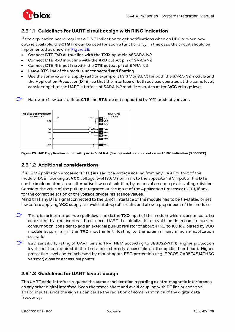
SARA-N2 series - System Integration Manual
UBX-17005143 - R04 Design-in Page 47 of 79
2.6.1.1 Guidelines for UART circuit design with RING indication
If the application board requires a RING indication to get notifications when an URC or when new
data is available, the CTS line can be used for such a functionality. In this case the circuit should be
implemented as shown in Figure 25:
Connect DTE TxD output line with the TXD input pin of SARA-N2
Connect DTE RxD input line with the RXD output pin of SARA-N2
Connect DTE RI input line with the CTS output pin of SARA-N2
Leave RTS line of the module unconnected and floating.
Use the same external supply rail (for example, at 3.3 V or 3.6 V) for both the SARA-N2 module and
the Application Processor (DTE), so that the interface of both devices operates at the same level,
considering that the UART interface of SARA-N2 module operates at the VCC voltage level
Hardware flow control lines CTS and RTS are not supported by "02" product versions.
TxD
Application Processor(3.3V DTE)
RxD
RI
GND
SARA-N2(DCE)
12 TXD
13 RXD
10 RTS
11 CTS
GND
0Ω TP
0Ω TP
52 VCC
3V33V3
VCC
51 VCC
53 VCC
Figure 25: UART application circuit with partial V.24 link (3-wire) serial communication and RING indication (3.3 V DTE)
2.6.1.2 Additional considerations
If a 1.8 V Application Processor (DTE) is used, the voltage scaling from any UART output of the
module (DCE), working at VCC voltage level (3.6 V nominal), to the apposite 1.8 V input of the DTE
can be implemented, as an alternative low-cost solution, by means of an appropriate voltage divider.
Consider the value of the pull-up integrated at the input of the Application Processor (DTE), if any,
for the correct selection of the voltage divider resistance values.
Mind that any DTE signal connected to the UART interface of the module has to be tri-stated or set
low before applying VCC supply, to avoid latch-up of circuits and allow a proper boot of the module.
There is no internal pull-up / pull-down inside the TXD input of the module, which is assumed to be
controlled by the external host once UART is initialized: to avoid an increase in current
consumption, consider to add an external pull-up resistor of about 47 k to 100 k, biased by VCC
module supply rail, if the TXD input is left floating by the external host in some application
scenario.
ESD sensitivity rating of UART pins is 1 kV (HBM according to JESD22-A114). Higher protection
level could be required if the lines are externally accessible on the application board. Higher
protection level can be achieved by mounting an ESD protection (e.g. EPCOS CA05P4S14THSG
varistor) close to accessible points.
2.6.1.3 Guidelines for UART layout design
The UART serial interface requires the same consideration regarding electro-magnetic interference
as any other digital interface. Keep the traces short and avoid coupling with RF line or sensitive
analog inputs, since the signals can cause the radiation of some harmonics of the digital data
frequency.
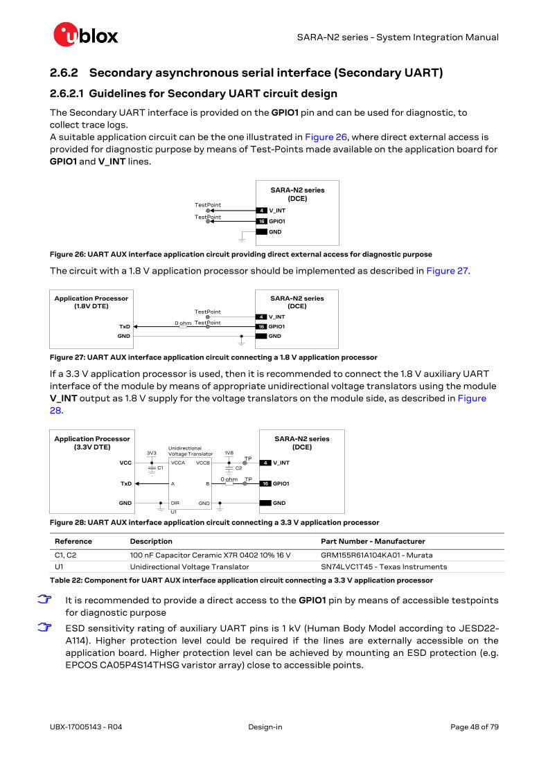
SARA-N2 series - System Integration Manual
UBX-17005143 - R04 Design-in Page 48 of 79
2.6.2 Secondary asynchronous serial interface (Secondary UART)
2.6.2.1 Guidelines for Secondary UART circuit design
The Secondary UART interface is provided on the GPIO1 pin and can be used for diagnostic, to
collect trace logs.
A suitable application circuit can be the one illustrated in Figure 26, where direct external access is
provided for diagnostic purpose by means of Test-Points made available on the application board for
GPIO1 and V_INT lines.
scaling
SARA-N2 series (DCE)
16 GPIO1
GND
TestPoint4 V_INT
TestPoint
Figure 26: UART AUX interface application circuit providing direct external access for diagnostic purpose
The circuit with a 1.8 V application processor should be implemented as described in Figure 27.
scaling
TxD
Application Processor(1.8V DTE)
SARA-N2 series (DCE)
16 GPIO1
GND GND
0 ohm TestPoint4 V_INT
TestPoint
Figure 27: UART AUX interface application circuit connecting a 1.8 V application processor
If a 3.3 V application processor is used, then it is recommended to connect the 1.8 V auxiliary UART
interface of the module by means of appropriate unidirectional voltage translators using the module
V_INT output as 1.8 V supply for the voltage translators on the module side, as described in Figure
28.
4 V_INT
TxD
Application Processor(3.3V DTE)
GND
SARA-N2 series (DCE)
16 GPIO1
GND
1V8
B A
GND
U1
VCCBVCCA
UnidirectionalVoltage Translator
C1 C2
3V3
DIR
VCC
0 ohm TP
TP
Figure 28: UART AUX interface application circuit connecting a 3.3 V application processor
Reference Description Part Number - Manufacturer
C1, C2 100 nF Capacitor Ceramic X7R 0402 10% 16 V GRM155R61A104KA01 - Murata
U1 Unidirectional Voltage Translator SN74LVC1T45 - Texas Instruments
Table 22: Component for UART AUX interface application circuit connecting a 3.3 V application processor
It is recommended to provide a direct access to the GPIO1 pin by means of accessible testpoints
for diagnostic purpose
ESD sensitivity rating of auxiliary UART pins is 1 kV (Human Body Model according to JESD22-
A114). Higher protection level could be required if the lines are externally accessible on the
application board. Higher protection level can be achieved by mounting an ESD protection (e.g.
EPCOS CA05P4S14THSG varistor array) close to accessible points.
SARA-N2 series - System Integration Manual
UBX-17005143 - R04 Design-in Page 49 of 79
2.6.3 DDC (I2C) interface
DDC (I2C) interface is not supported by the "02" version of the product.
2.7 General Purpose Input/Output (GPIO)
A typical usage of SARA-N2 series modules’ GPIOs follows:
GPIO1 pin providing secondary UART data output, available to collect trace diagnostic logs
delivered by the module: it is recommended to provide a direct access to the GPIO1 pin by means
of an accessible testpoint for diagnostic purposes (see sections 1.9.2 and 2.6.2)
CTS pin set as Network Indicator (see Figure 29 / Table 23 below) or Ring Indicator (see section
2.6.1.1)
SARA-N2 series
CTSR1
R3
3V6
Network Indicator
R2
11
DL1
T1
TestPoint
GPIO1 16Secondary UART for Diagnostic
Figure 29: Application circuit for network indication provided over CTS
Reference Description Part Number - Manufacturer
R1 10 k resistor 0402 5% 0.1 W Various manufacturers
R2 47 k resistor 0402 5% 0.1 W Various manufacturers
R3 820 resistor 0402 5% 0.1 W Various manufacturers
DL1 LED red SMT 0603 LTST-C190KRKT - Lite-on Technology Corporation
T1 NPN BJT Transistor BC847 - Infineon
Table 23: Components for network indication application circuit
Use transistors with at least an integrated resistor in the base pin or otherwise put a 10 kΩ resistor
on the board in series to the GPIO of SARA-N2 series modules.
Do not apply voltage to any GPIO of the module before the switch-on of the GPIO’s supply (V_INT),
to avoid latch-up of circuits and allow a proper boot of the module.
ESD sensitivity rating of the GPIO pins is 1 kV (Human Body Model according to JESD22-A114).
A higher protection level could be required if the lines are externally accessible and it can be
achieved by mounting an ESD protection (e.g. EPCOS CA05P4S14THSG varistor array) close to
accessible points.
If GPIO pins are not used, they can be left unconnected on the application board, but it is
recommended to provide direct access to the GPIO1 pin by means of accessible testpoints for
diagnostic purposes.
2.8 Reserved pins (RSVD)
SARA-N2 series modules have pins reserved for future use, marked as RSVD.
All the RSVD pins are to be left unconnected on the application board, except for the RSVD pin
number 33 that can be externally connected to ground.

SARA-N2 series - System Integration Manual
UBX-17005143 - R04 Design-in Page 50 of 79
2.9 Module placement
Optimize placement for minimum length of RF line and closer path from DC source for VCC.
Make sure that the module, RF and analog parts / circuits are clearly separated from any possible
source of radiated energy, including digital circuits that can radiate some digital frequency
harmonics, which can produce Electro-Magnetic Interference affecting module, RF and analog parts
/ circuits’ performance or implement proper countermeasures to avoid any possible Electro-
Magnetic Compatibility issue.
Make sure that the module, RF and analog parts / circuits, high speed digital circuits are clearly
separated from any sensitive part / circuit which may be affected by Electro-Magnetic Interference
or employ countermeasures to avoid any possible Electro-Magnetic Compatibility issue.
Provide enough clearance between the module and any external part: clearance of at least 0.4 mm
per side is recommended to permit suitable mounting of the parts.
2.10 Module footprint and paste mask
Figure 30 and Table 24 describe the suggested footprint (i.e. copper mask) and paste mask layout
for SARA modules: the proposed land pattern layout reflects the modules’ pins layout, while the
proposed stencil apertures layout is slightly different (see the F’’, H’’, I’’, J’’, O’’ parameters compared
to the F’, H’, I’, J’, O’ ones).
The Non Solder Mask Defined (NSMD) pad type is recommended over the Solder Mask Defined
(SMD) pad type, implementing the solder mask opening 50 µm larger per side than the
corresponding copper pad.
The recommended solder paste thickness is 150 µm, according to application production process
requirements.
K
M1
M1
M2
E G H’ J’ EANT pin
B
Pin 1
K
G
H’
J’
A
D
D
O’
O’
L N L
I’
F’
F’
K
M1
M1
M2
E G H’’ J’’ EANT pin
B
Pin 1
K
G
H’’
J’’
A
D
D
O’’
O’’
L N L
I’’
F’’
F’’
Stencil: 150 µm
Figure 30: SARA-N2 series modules suggested footprint and paste mask (application board top view)

SARA-N2 series - System Integration Manual
UBX-17005143 - R04 Design-in Page 51 of 79
Parameter Value Parameter Value Parameter Value
A 26.0 mm G 1.10 mm K 2.75 mm
B 16.0 mm H’ 0.80 mm L 2.75 mm
C 3.00 mm H’’ 0.75 mm M1 1.80 mm
D 2.00 mm I’ 1.50 mm M2 3.60 mm
E 2.50 mm I’’ 1.55 mm N 2.10 mm
F’ 1.05 mm J’ 0.30 mm O’ 1.10 mm
F’’ 1.00 mm J’’ 0.35 mm O’’ 1.05 mm
Table 24: SARA-N2 series modules suggested footprint and paste mask dimensions
These are recommendations only and not specifications. The exact copper, solder and paste mask
geometries, distances, stencil thicknesses and solder paste volumes must be adapted to the
specific production processes (e.g. soldering etc.) of the customer.
2.11 SARA-N211 integration in devices intended for use in
potentially explosive atmospheres
2.11.1 General guidelines
SARA-N211 modules are certified as components intended for use in potentially explosive
atmospheres (see section 4.3 and see the “Approvals” section of the SARA-N2 series Data Sheet [1]
for further details), with the following marking:
Ex II 1G, Ex ia IIC
According to the marking stated above, SARA-N211 modules are certified as electrical equipment of:
group “II”: intended for use in areas with explosive gas atmosphere other than mines susceptible
to firedamp.
category “1G”: intended for use in zone 0 hazardous areas, in which an explosive atmospheres is
caused by mixtures of air and gases, or when vapours or mists are continuously or frequently
present for long periods. The modules are also suitable for applications intended for use in zone 1
and zone 2 hazardous areas.
level of protection “ia”: intrinsically safe apparatus with very high level of protection, not capable
of causing ignition in normal operation and with the application of one countable fault or a
combination of any two countable fault plus those non-countable faults which give the most
onerous condition.
subdivision “IIC”: intended for use in areas where the nature of the explosive gas atmosphere is
considered very dangerous based on the Maximum Experimental Safe Gap or the Minimum
Ignition Current ratio of the explosive gas atmosphere in which the equipment may be installed
(typical gases are hydrogen, acetylene, carbon disulphide), so that the modules are also suitable
for applications intended for use in subdivision IIB (typical gases are ethylene, coke oven gas and
other industrial gases) and subdivision IIA (typical gases are industrial methane, propane, petrol
and the majority of industrial gases).
The temperature range of use of SARA-N211 modules is defined in the “Operating temperature
range” section of the SARA-N2 series Data Sheet [1]. The modules are suitable for temperature class
T4 applications, as long as the maximum input power does not exceed 2.0 W.
Even if SARA-N211 modules are certified as components intended for use in potentially explosive
atmospheres as described above, the application device that integrates the module must be

SARA-N2 series - System Integration Manual
UBX-17005143 - R04 Design-in Page 52 of 79
approved under all the certification schemes required by the specific application device that will be
deployed in the market as apparatus intended for use in potentially explosive atmospheres.
The certification scheme approvals required for the application device integrating SARA-N211
module, intended for use in potentially explosive atmospheres, may differ depending on the
following topics:
the country or the region where the application device must be deployed
the classification of the application device in relation to the use in potentially explosive
atmospheres
the classification of the hazardous areas in which the application device is intended for use
Any specific applicable requirement for the implementation of the apparatus integrating SARA-
N211 module, intended for use in potentially explosive atmospheres, must be fulfilled according to
the exact applicable standards: check the detailed requisites on the pertinent norms for the
application, as for example the IEC 60079-0 [15], IEC 60079-11[16], IEC 60079-26 [17] standards.
The certification of the application device that integrates a SARA-N211 module and the
compliance of the application device with all the applicable certification schemes, directives and
standards required for use in potentially explosive atmospheres are the sole responsibility of the
application device manufacturer.
The application device integrating a SARA-N211 module for use in potentially explosive atmospheres
must be designed so that any circuit/part of the apparatus shall not invalidate the specific
characteristics of the type of protection of the module.
The intrinsic safety “i” type of protection of SARA-N211 modules is based on the restriction of the
electrical energy within equipment and of the interconnecting wiring exposed to the explosive
atmosphere to a level below that which can cause ignition by either sparking or heating effects.
The following input and equivalent parameters must be considered integrating a SARA-N211 module
in an application device intended for use in potentially explosive atmospheres:
Total internal capacitance, Ci (see Table 25)
Total internal inductance, Li (see Table 25)
The module does not contain blocks which increase the voltage (e.g. like step-up, duplicators,
boosters, etc.)
The nameplate of SARA-N211 modules is described in the “Product labeling” section of the SARA-N2
series Data Sheet [1]. For additional info and modules’ certificate of compliancy for use in potentially
explosive atmospheres, see our website (www.u-blox.com) or contact the u-blox office or sales
representative nearest you.
The final enclosure of the application device integrating SARA-N211 modules, intended for use in
potentially explosive atmospheres, must guarantee a minimum degree of ingress protection of
IP20.

SARA-N2 series - System Integration Manual
UBX-17005143 - R04 Design-in Page 53 of 79
2.11.2 Guidelines for VCC supply circuit design
The power supply ratings, average and pulse, must be considered in the design of the VCC supply
circuit on the application device integrating SARA-N211 module, implementing proper circuits
providing adequate maximum voltage and current to the VCC supply input of the modules,
according to the specific potentially explosive gas atmosphere category subdivision where the
apparatus is intended for use.
Table 25 lists the maximum input and equivalent parameters that must be considered in the sub-
division IIC, the sub-division IIB and the sub-division IIA for SARA-N211 modules.
Parameter SARA-N211
Ui 4.2 V
Ii 0.5 A
Ci 68.1 µF
Li 8.5 µH
Table 25: Maximum input and equivalent parameters for sub-division IIC
Primary and secondary cells and batteries
Cells and batteries incorporated into equipment with intrinsic safety “i” protection to potentially
explosive gas atmosphere shall conform to the requirements of the IEC 60079-0 [15],
IEC 60079-11 [16] ATEX standards.
Shunt voltage limiters
For Level of Protection “ia”, the application of controllable semiconductor components as shunt
voltage limiting devices, for example transistors, thyristors, voltage/current regulators, etc., may be
permitted if both the input and output circuits are intrinsically safe circuits or where it can be shown
that they cannot be subjected to transients from the power supply network. In circuits complying
with the above, two devices are considered to be an infallible assembly.
For Level of Protection “ia”, three independent active voltage limitation semiconductor circuits may
be used in associated apparatus provided the transient conditions of the clause 7.5.1 of IEC 60079-11
standard are met. These circuits shall also be tested in accordance with the clause 10.1.5.3 of the IEC
60079-11 standard [16].
Series current limiters
The use of three series blocking diodes in circuits of Level of Protection “ia” is permitted, however,
other semiconductors and controllable semiconductor devices shall be used as series current-
limiting devices only in Level of Protection “ib” or “ic” apparatus. However, for power limitation
purposes, Level of Protection “ia” apparatus may use series current limiters consisting of
controllable and non-controllable semiconductor devices.
The use of semiconductors and controllable semiconductor devices as current-limiting devices for
spark ignition limitation is not permitted for Level of Protection “ia” apparatus because of their
possible use in areas in which a continuous or frequent presence of an explosive atmosphere may
coincide with the possibility of a brief transient which could cause ignition. The maximum current
that may be delivered may have a brief transient but will not be taken as Io, because the compliance
with the spark ignition test of the clause 10.1 of IEC 60079-11 standard [16] would have established
the successful limitation of the energy in this transient.
Protection against polarity reversal
Protection against polarity reversal shall be provided within intrinsically safe apparatus to prevent
invalidation of the type of protection as a result of reversal of the polarity of supplies to that
intrinsically safe apparatus or at connections between cells of a battery where this could occur. For
this purpose, single diode shall be acceptable.

SARA-N2 series - System Integration Manual
UBX-17005143 - R04 Design-in Page 54 of 79
Other considerations
All the recommendations reported in section 2.11.1 must be considered for the implementation of the
VCC supply circuit on application integrating SARA-N211 modules intended for use in potentially
explosive atmospheres. Any specific applicable requirement for the VCC supply circuit design must
be fulfilled according to all the exact applicable standards for the apparatus.
Check the detailed requisites on the pertinent norms for the application apparatus, as for example
the IEC 60079-0 [15], IEC 60079-11 [16], IEC 60079-26 [17] standards.
2.11.3 Guidelines for antenna RF interface design
The RF radiating power of SARA-N211 modules is compliant to all the applicable 3GPP / ETSI
standards, with a maximum of 250 mW RF average power according to the LTE Cat NB1 Power Class
stated in Table 2.
The RF threshold power of the application device integrating a SARA-N211 module is defined,
according to the IEC 60079-0 ATEX standard [15], as the product of the effective output power of
the module multiplied by the antenna gain (implemented/used on the application device).
The RF threshold power of the application device integrating a SARA-N211 module must not exceed
the limits shown in Table 26, according to the IEC 60079-0 ATEX standard [15].
Gas group II subdivision RF threshold power limits according to the IEC 60079-0 ATEX standard
IIA (a typical gas is propane) 6.0 W
IIB (a typical gas is ethylene) 3.5 W
IIC (a typical gas is hydrogen) 2.0 W
Table 26: RF threshold power limits for the different gas group II subdivisions according to the IEC 60079-0 ATEX standard [15]
The system antenna(s) implemented/used on the application device integrating SARA-N211
module must be designed/selected so that the antenna gain (i.e. the combined transmission line,
connector, cable losses and radiating element gain) multiplied by the output power of the module
does not exceed the limits shown in Table 26.

SARA-N2 series - System Integration Manual
UBX-17005143 - R04 Design-in Page 55 of 79
2.12 Schematic for SARA-N2 series module integration
Figure 31 is an example of a schematic diagram where a SARA-N2 series module “02” product
version is integrated into an application board, using all the available interfaces and functions of the
module.
3V6
GND100uF 10nF
SARA-N2 series
52 VCC
53 VCC
51 VCC
68pF
SDA
SCL
26
27RSVD
GND
18 RESET_N
Application Processor
Open drain
output
TP
12 TXD
13 RXD
10 RTS
11 CTS
TP
TPTXD
RXD
RI
3.6V DTE
GND
0Ω
0Ω47pF
SIM Card Holder
CCVCC (C1)
CCVPP (C6)
CCIO (C7)
CCCLK (C3)
CCRST (C2)
GND (C5)47pF 47pF 100nF
41VSIM
39SIM_IO
38SIM_CLK
40SIM_RST
47pF
4V_INT
ESD ESD ESD ESD
Test-Point
62ANT_DET10k
27pF ESD
68nH
56
ConnectorExternal antenna33pF
ANT
39nH
15pF
24
16
GPIO2
GPIO1
15pF100nF
VCC
3V6
Test-Point
Network Indicator
3V6
GND
Figure 31: Example of schematic diagram to integrate a SARA-N2 module “02” product version using all available interfaces
2.13 Design-in checklist
2.13.1 Schematic checklist
The following are the most important points for a simple schematic check:
DC supply must provide a nominal voltage at VCC pin above the minimum operating range
limit.
DC supply must be capable of providing, at VCC pins, the specified average current during a
transmission at maximum power with a voltage level above the minimum operating range
limit.
VCC supply should be clean, with very low ripple/noise.
Do not apply loads which might exceed the limit for maximum available current from V_INT
supply.
Check that voltage level of any connected pin does not exceed the relative operating range.
Capacitance and series resistance must be limited on each SIM signal to match the SIM
specifications.
SARA-N2 series - System Integration Manual
UBX-17005143 - R04 Design-in Page 56 of 79
Insert the suggested capacitors on each SIM signal and low capacitance ESD protections if
accessible.
Check UART signals direction, since the signal names follow the ITU-T V.24 Recommendation [5].
Provide accessible testpoints directly connected to the following pins: TXD, RXD, GPIO1,
V_INT and RESET_N for diagnostic purpose.
Provide proper precautions for ESD immunity as required on the application board.
Any external signal connected to the UART interface pin must be tri-stated or set low before
applying VCC supply, to avoid latch-up of circuits and let a proper boot of the module.
Any external signal connected to any generic digital interface pin (GPIO, I2C) must be tri-
stated or set low when the module is in not-powered mode and during the module power-on
sequence (at least until the activation of the V_INT output), to avoid latch-up of circuits and
let a proper boot of the module.
All unused pins can be left unconnected.
2.13.2 Layout checklist
The following are the most important points for a simple layout check:
Check 50 nominal characteristic impedance of the RF transmission line connected to the
ANT pad (antenna RF input/output interface).
Follow the recommendations of the antenna producer for correct antenna installation and
deployment (PCB layout and matching circuitry).
Ensure no coupling occurs between the RF interface and noisy or sensitive signals (like SIM
signals and high-speed digital lines).
VCC line should be wide and short.
Route VCC supply line away from sensitive analog signals.
Ensure proper grounding.
Optimize placement for minimum length of RF line and closer path from DC source for VCC.
Keep routing short and minimize parasitic capacitance on the SIM lines to preserve signal
integrity.
2.13.3 Antenna checklist
Antenna termination should provide 50 characteristic impedance with V.S.W.R at least
less than 3:1 (recommended 2:1) on operating bands in deployment geographical area.
Follow the recommendations of the antenna producer for correct antenna installation and
deployment (PCB layout and matching circuitry).
Ensure compliance with any regulatory agency RF radiation requirement.

SARA-N2 series - System Integration Manual
UBX-17005143 - R04 Handling and soldering Page 57 of 79
3 Handling and soldering
No natural rubbers, no hygroscopic materials or materials containing asbestos are employed.
3.1 Packaging, shipping, storage and moisture preconditioning
For information pertaining to reels and tapes, Moisture Sensitivity levels (MSD), shipment and
storage information, as well as drying for preconditioning see the SARA-N2 series Data Sheet [1] and
the u-blox Package Information Guide [2].
3.2 Handling
The SARA-N2 series modules are Electro-Static Discharge (ESD) sensitive devices.
Ensure ESD precautions are implemented during handling of the module.
Electrostatic discharge (ESD) is the sudden and momentary electric current that flows between two
objects at different electrical potentials caused by direct contact or induced by an electrostatic field.
The term is usually used in the electronics and other industries to describe momentary unwanted
currents that may cause damage to electronic equipment.
The ESD sensitivity for each pin of SARA-N2 series modules (as Human Body Model according to
JESD22-A114F) is specified in the SARA-N2 series Data Sheet [1].
ESD prevention is based on establishing an Electrostatic Protective Area (EPA). The EPA can be a
small working station or a large manufacturing area. The main principle of an EPA is that there are
no highly charging materials near ESD sensitive electronics, all conductive materials are grounded,
workers are grounded, and charge build-up on ESD sensitive electronics is prevented. International
standards are used to define typical EPA and can be obtained for example from International
Electrotechnical Commission (IEC) or American National Standards Institute (ANSI).
In addition to standard ESD safety practices, the following measures should be taken into account
whenever handling the SARA-N2 series modules:
Unless there is a galvanic coupling between the local GND (i.e. the work table) and the PCB GND,
then the first point of contact when handling the PCB must always be between the local GND and
PCB GND.
Before mounting an antenna patch, connect ground of the device.
When handling the module, do not come into contact with any charged capacitors and be careful
when contacting materials that can develop charges (e.g. patch antenna, coax cable, soldering
iron,…).
To prevent electrostatic discharge through the RF pin, do not touch any exposed antenna area. If
there is any risk that such exposed antenna area is touched in non ESD protected work area,
implement proper ESD protection measures in the design.
When soldering the module and patch antennas to the RF pin, make sure to use an ESD safe
soldering iron.
SARA-N2 series - System Integration Manual
UBX-17005143 - R04 Handling and soldering Page 58 of 79
3.3 Soldering
3.3.1 Soldering paste
Use of "No Clean" soldering paste is strongly recommended, as it does not require cleaning after the
soldering process has taken place. The paste listed in the example below meets these criteria.
Soldering Paste: OM338 SAC405 / Nr.143714 (Cookson Electronics)
Alloy specification: 95.5% Sn / 3.9% Ag / 0.6% Cu (95.5% Tin / 3.9% Silver / 0.6% Copper)
95.5% Sn / 4.0% Ag / 0.5% Cu (95.5% Tin / 4.0% Silver / 0.5% Copper)
Melting Temperature: 217 °C
Stencil Thickness: 150 µm for base boards
The final choice of the soldering paste depends on the approved manufacturing procedures.
The paste-mask geometry for applying soldering paste should meet the recommendations in
section 2.10.
The quality of the solder joints should meet the appropriate IPC specification.
3.3.2 Reflow soldering
A convection type-soldering oven is strongly recommended over the infrared type radiation oven.
Convection heated ovens allow precise control of the temperature and all parts will be heated up
evenly, regardless of material properties, thickness of components and surface color.
Consider the "IPC-7530 Guidelines for temperature profiling for mass soldering (reflow and wave)
processes, published 2001".
Reflow profiles are to be selected according to the following recommendations.
Failure to observe these recommendations can result in severe damage to the device!
Preheat phase
Initial heating of component leads and balls. Residual humidity will be dried out. Note that this
preheat phase will not replace prior baking procedures.
Temperature rise rate: max 3 °C/s If the temperature rise is too rapid in the preheat phase it
may cause excessive slumping.
Time: 60 to 120 s If the preheat is insufficient, rather large solder balls tend
to be generated. Conversely, if performed excessively, fine
balls and large balls will be generated in clusters.
End Temperature: 150 to 200 °C If the temperature is too low, non-melting tends to be
caused in areas containing large heat capacity.
Heating/ reflow phase
The temperature rises above the liquidus temperature of 217 °C. Avoid a sudden rise in temperature
as the slump of the paste could become worse.
Limit time above 217 °C liquidus temperature: 40 to 60 s
Peak reflow temperature: 245 °C
Cooling phase
A controlled cooling avoids negative metallurgical effects (solder becomes more brittle) of the solder
and possible mechanical tensions in the products. Controlled cooling helps to achieve bright solder
fillets with a good shape and low contact angle.
Temperature fall rate: max 4 °C/s
To avoid falling off, modules should be placed on the topside of the motherboard during soldering.
The soldering temperature profile chosen at the factory depends on additional external factors like
choice of soldering paste, size, thickness and properties of the base board, etc.
SARA-N2 series - System Integration Manual
UBX-17005143 - R04 Handling and soldering Page 59 of 79
Exceeding the maximum soldering temperature and the maximum liquidus time limit in the
recommended soldering profile may permanently damage the module.
Preheat Heating Cooling
[°C] Peak Temp. 245°C [°C]
## ##
Liquidus Temperature
217 217
## ##
40 - 60 s
End Temp. max 4°C/s
150 - 200°C
150 150
max 3°C/s 60 - 120 s
100 Typical Leadfree 100
Soldering Profile
50 50
Elapsed time [s] Figure 32: Recommended soldering profile
SARA-N2 series modules must not be soldered with a damp heat process.
3.3.3 Optical inspection
After soldering the module, inspect it optically to verify that the module is properly aligned and
centered.
3.3.4 Cleaning
Cleaning the soldered modules is not recommended. Residues underneath the modules cannot be
easily removed with a washing process.
Cleaning with water will lead to capillary effects where water is absorbed in the gap between the
baseboard and the module. The combination of residues of soldering flux and encapsulated water
leads to short circuits or resistor-like interconnections between neighboring pads. Water will also
damage the sticker and the ink-jet printed text.
Cleaning with alcohol or other organic solvents can result in soldering flux residues flooding into
the two housings, areas that are not accessible for post-wash inspections. The solvent will also
damage the sticker and the ink-jet printed text.
Ultrasonic cleaning will permanently damage the module, in particular the quartz oscillators.
For best results use a "no clean" soldering paste and eliminate the cleaning step after the soldering.
3.3.5 Repeated reflow soldering
Repeated reflow soldering processes and soldering the module upside down are not recommended.
Boards with components on both sides may require two reflow cycles. In this case, the module
should always be placed on the side of the board that is submitted into the last reflow cycle. The
reason for this (besides others) is the risk of the module falling off due to the significantly higher
weight in relation to other components.
u-blox gives no warranty against damages to the SARA-N2 series modules caused by performing
more than a total of two reflow soldering processes (one reflow soldering process to mount the
SARA-N2 series module, plus one reflow soldering process to mount other parts).
SARA-N2 series - System Integration Manual
UBX-17005143 - R04 Handling and soldering Page 60 of 79
3.3.6 Wave soldering
SARA-N2 series LGA modules must not be soldered with a wave soldering process.
Boards with combined through-hole technology (THT) components and surface-mount technology
(SMT) devices require wave soldering to solder the THT components. No more than one wave
soldering process is allowed for board with a SARA-N2 series module already populated on it.
Performing a wave soldering process on the module can result in severe damage to the device!
u-blox gives no warranty against damages to the SARA-N2 series modules caused by performing
more than a total of two soldering processes (one reflow soldering process to mount the SARA-N2
series module, plus one wave soldering process to mount other THT parts on the application
board).
3.3.7 Hand soldering
Hand soldering is not recommended.
3.3.8 Rework
Rework is not recommended.
Never attempt a rework on the module itself, e.g. replacing individual components. Such actions
immediately terminate the warranty.
3.3.9 Conformal coating
Certain applications employ a conformal coating of the PCB using HumiSeal® or other related
coating products.
These materials affect the RF properties of the SARA-N2 series modules and it is important to
prevent them from flowing into the module.
The RF shields do not provide 100% protection for the module from coating liquids with low viscosity,
therefore care is required in applying the coating.
Conformal Coating of the module will void the warranty.
3.3.10 Casting
If casting is required, use viscose or another type of silicon pottant. The OEM is strongly advised to
qualify such processes in combination with the SARA-N2 series modules before implementing this
in the production.
Casting will void the warranty.
3.3.11 Grounding metal covers
Attempts to improve grounding by soldering ground cables, wick or other forms of metal strips
directly onto the EMI covers is done at the customer's own risk. The numerous ground pins should
be sufficient to provide optimum immunity to interferences and noise.
u-blox gives no warranty for damages to the SARA-N2 series modules caused by soldering metal
cables or any other forms of metal strips directly onto the EMI covers.
3.3.12 Use of ultrasonic processes
SARA-N2 series modules contain components which are sensitive to Ultrasonic Waves. Use of any
Ultrasonic Processes (cleaning, welding etc.) may cause damage to the module.
u-blox gives no warranty against damages to the SARA-N2 series modules caused by any
Ultrasonic Processes.

SARA-N2 series - System Integration Manual
UBX-17005143 - R04 Approvals Page 61 of 79
4 Approvals
4.1 Approvals overview
Product certification approval is the process of certifying that a product has passed all tests and
criteria required by specifications, typically called “certification schemes”, which can be divided into
three distinct categories:
Regulatory certification
o Country-specific approval required by local government in most regions and countries, such
as:
CE (Conformité Européenne) marking for European Union
FCC (Federal Communications Commission) approval for United States
NCC (National Communications Commission) approval for Taiwan
Industry certification
o Telecom industry-specific approval verifying the interoperability between devices and
networks:
GCF (Global Certification Forum), partnership between mainly European device
manufacturers and network operators to ensure and verify global interoperability between
devices and networks
PTCRB (PCS Type Certification Review Board), created by United States network operators
to ensure and verify interoperability between devices and North America networks
Operator certification
Operator-specific approvals required by some mobile network operator, such as:
China Telecom network operator in China
AT&T network operator in United States
Table 27 lists the main approvals of SARA-N2 series modules.
Certification Scheme SARA-N200 SARA-N201 SARA-N210 SARA-N211 SARA-N280
CE (European Conformity) • • •
GCF (Global Certification Forum) •
CCC (China Compulsory Certification) • •
SRRC (State Radio Regulation of China) • •
NCC (National Communications Commission
Taiwan) • • •
Anatel (Agência Nacional de Telecomunicações
Brazil) •
RCM (Regulatory Compliance Mark Australia) •
NBTC (Thailand Regulatory Certification) •
IMDA (Singapore Regulatory Certification) •
ATEX (Atmosphere Explosive) •
China Telecom (Chinese Network Operator) •
China Unicom (Chinese Network Operator) •
Deutsche Telekom (German Network Operator) • • •
Table 27: SARA-N2 series main certification approvals
For all the certificates of compliancy and for the complete list of approvals (including countries’
and network operators’ approvals) of SARA-N2 series modules, see our website
(http://www.u-blox.com/) or contact the u-blox office or sales representative nearest you.

SARA-N2 series - System Integration Manual
UBX-17005143 - R04 Approvals Page 62 of 79
Even if SARA-N2 series modules are approved under all major certification schemes, the application
device that integrates SARA-N2 series modules must also be approved under all the certification
schemes required by the specific application device to be deployed in the market.
The required certification scheme approvals and relative testing specifications differ depending on
the country or the region where the device that integrates SARA-N2 series modules is intended to
be deployed, on the relative vertical market of the device, on type, features and functionalities of the
whole application device, and on the network operators where the device is intended to operate.
The u-blox cellular module’s approval can be re-used for the approval of the integrating application
device, but the possible re-use depends on the physical characteristics of the integrating application
device, also considering the configuration used for the approvals of SARA-N2 series modules, and it
also depends on related certification scheme approvals required for the integrating application
device as explained above.
Check the appropriate applicability of the SARA-N2 series module’s approvals while starting the
certification process of the device integrating the module: the re-use of the u-blox cellular
module’s approval can significantly reduce the cost and time to market of the application device
certification.
The certification of the application device that integrates a SARA-N2 series module and the
compliance of the application device with all the applicable certification schemes, directives and
standards are the sole responsibility of the application device manufacturer.
4.2 European Conformance CE mark
SARA-N200, SARA-N210 and SARA-N211 modules have been evaluated against the essential
requirements of the Radio Equipment Directive 2014/53/EU.
In order to satisfy the essential requirements of the 2014/53/EU RED, the modules are compliant
with the following standards:
Radio Spectrum Efficiency (Article 3.2):
o EN 301 908-1
o EN 301 908-13
Electromagnetic Compatibility (Article 3.1b):
o EN 301 489-1
o EN 301 489-52
Health and Safety (Article 3.1a)
o EN 62368-1
o EN 62311
Radiofrequency radiation exposure Information: this equipment complies with radiation exposure
limits prescribed for an uncontrolled environment for fixed and mobile use conditions. This
equipment should be installed and operated with a minimum distance of 20 cm between the
radiator and the body of the user or nearby persons. This transmitter must not be co-located or
operating in conjunction with any other antenna or transmitter except as authorized in the
certification of the product.
The gain of the system antenna(s) used for the SARA-N200, SARA-N210 and SARA-N211 modules
(i.e. the combined transmission line, connector, cable losses and radiating element gain) must not
exceed the values stated in the Declaration of Conformity of the modules, for mobile and fixed or
mobile operating configurations:
9.2 dBi in 800 MHz, i.e. LTE FDD-20 band
9.4 dBi in 900 MHz, i.e. LTE FDD-8 band
SARA-N2 series - System Integration Manual
UBX-17005143 - R04 Approvals Page 63 of 79
The conformity assessment procedure for SARA-N200 and SARA-N210 modules, referred to in
Article 17 and detailed in Annex II of Directive 2014/53/EU, has been followed.
Thus, the following marking is included in the product:
The conformity assessment procedure for SARA-N211 modules, referred to in Article 17 and detailed
in Annex II of Directive 2014/53/EU, has been followed. According to the ATEX Directive 2014/34/EU,
Article 13, Paragraph 1-3, the CE mark is not affixed to the product label.
The following marking is included in the product:
1304
4.3 ATEX conformance
SARA-N211 modules are certified as components intended for use in potentially explosive
atmospheres compliant to the following standards:
IEC 60079-0
IEC 60079-11
IEC 60079-26
The certification numbers of the modules, according to the ATEX directive 2014/34/EU, are:
SIQ 18 ATEX 104 U
The certification numbers of the modules, according to the IECEx conformity assessment system,
are:
IECEx SIQ 18.0004U
According to the standards listed above, SARA-N211 modules are certified with the following
marking:
Ex II 1G, Ex ia IIC
The temperature range for using SARA-N211 modules is defined in the “Operating temperature
range” section of the SARA-N2 series Data Sheet [1]. The modules are suitable for temperature class
T4 applications, as long as the maximum input power does not exceed 2.0 W on SARA-N211 modules.
The RF radiating profile of SARA-N211 modules is compliant to all the applicable 3GPP / ETSI
standards, with a maximum of 250 mW RF average power according to the LTE Cat NB1 Power Class
stated in Table 2.
The nameplate of SARA-N211 modules is described in the “Product labeling” section of the SARA-N2
series Data Sheet [1].
Table 28 lists the maximum input and equivalent parameters that must be considered in the sub-
division IIC, the sub-division IIB and the sub-division IIA for SARA-N211 modules.
Parameter SARA-N211
Ui 4.2 V
Ii 0.5 A
Ci 68.1 µF
Li 8.5 µH
Table 28: Maximum input and equivalent parameters for sub-division IIC, IIB and IIA

SARA-N2 series - System Integration Manual
UBX-17005143 - R04 Approvals Page 64 of 79
4.4 Chinese conformance
SARA-N200 and SARA-N201 modules have the applicable regulatory approval for China:
CMIIT ID: 2018CJ1113
4.5 Taiwanese conformance
SARA-N200, SARA-N211 and SARA-N280 modules have the applicable regulatory approval for
Taiwan (NCC)
SARA-N200 modules NCC ID: CCAI17Z10210T5
CCAI17Z10210T5
SARA-N211 modules NCC ID: CCAI17Z10270T0
CCAI17Z10270T0
SARA-N280 modules NCC ID: CCAI17Z10200T2
CCAI17Z10200T2

SARA-N2 series - System Integration Manual
UBX-17005143 - R04 Product testing Page 65 of 79
5 Product testing
5.1 u-blox in-series production test
u-blox focuses on high quality for its products. All units produced are fully tested. Defective units are
analyzed in detail to improve the production quality.
This is achieved with automatic test equipment, which delivers a detailed test report for each unit.
The following measurements are done:
Digital self-test (firmware download, Flash firmware verification, IMEI programming)
Measurement of voltages and currents
Functional tests (serial interface communication, real time clock)
Digital tests (GPIOs, digital interfaces)
Measurement and calibration of RF characteristics in all supported bands (Receiver S/N
verification, frequency tuning of reference clock, calibration of transmitter and receiver power
levels)
Verification of RF characteristics after calibration (modulation accuracy, power levels and
spectrum performance are checked to be within tolerances when calibration parameters are
applied)
Figure 33: Automatic test equipment for module tests
5.2 Test parameters for OEM manufacturer
Because of the testing done by u-blox (with 100% coverage), an OEM manufacturer does not need to
repeat firmware tests or measurements of the module RF performance or tests over analog and
digital interfaces in their production test.
An OEM manufacturer should focus on:
Module assembly on the device; it should be verified that:
Soldering and handling process did not damaged the module components
All module pins are well soldered on device board
There are no short circuits between pins
Component assembly on the device; it should be verified that:
Communication with host controller can be established
The interfaces between module and device are working
Overall RF performance test of the device including antenna

SARA-N2 series - System Integration Manual
UBX-17005143 - R04 Product testing Page 66 of 79
Dedicated tests can be implemented to check the device. For example, AT commands can be used
to perform functional tests on the digital interfaces (communication with the host controller, check
the SIM interface, GPIOs, etc.) or to perform RF performance tests (see the following section 5.2.2
for details).
5.2.1 “Go/No go” tests for integrated devices
A “Go/No go” test is typically used to compare the signal quality with a “Golden Device” in a location
with excellent network coverage and known signal quality. This test should be performed after the
data connection has been established. AT+CSQ is the typical AT command used to check signal
quality in term of Received Signal Strength Indication (RSSI). See the SARA-N2 series AT
Commands Manual [3] for the AT+CSQ command syntax description and usage.
These kinds of test may be useful as a “go/no go” test but not for RF performance measurements.
This test is suitable to check the functionality of communications with the host controller, the SIM
card and the power supply. It is also a means to verify if components at the antenna interface are
well-soldered.
5.2.2 RF functional tests
The overall RF functional test of the device including the antenna can be performed with basic
instruments such as a spectrum analyzer (or an RF power meter) and a signal generator with the
assistance of the AT+UTEST command over the AT command user interface.
The AT+UTEST command provides a simple interface to set the module to Rx or Tx test modes
ignoring the cellular signaling protocol. The command can set the module into:
transmitting mode in a specified channel and power level in all supported bands
receiving mode in a specified channel to return the measured power level in all supported bands
See the SARA-N2 series AT Commands Manual [3] for the AT+UTEST command description and
usage.
This feature allows the measurement of the transmitter and receiver power levels to check the
component assembly related to the module antenna interface and to check other device interfaces
on which the RF performance depends.
To avoid module damage during a transmitter test, a suitable antenna according to module
specifications or a 50 termination must be connected to the ANT port.
To avoid module damage during a receiver test, the maximum power level received at the ANT port
must meet module specifications.
The AT+UTEST command sets the module to emit RF power ignoring cellular signaling protocol.
This emission can generate interference that can be prohibited by law in some countries. The use
of this feature is intended for testing purposes in controlled environments by qualified users and
must not be used during the normal module operation. Follow the instructions suggested in the
u-blox documentation. u-blox assumes no responsibilities for the inappropriate use of this feature.
Figure 34 illustrates a typical test setup for such an RF functional test.
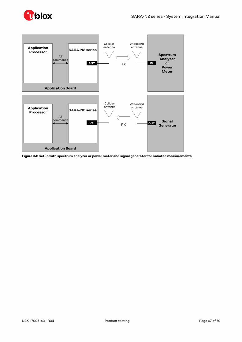
SARA-N2 series - System Integration Manual
UBX-17005143 - R04 Product testing Page 67 of 79
Application Board
SARA-N2 series
ANT
Application Processor
AT commands
Cellular antenna
SpectrumAnalyzer
orPowerMeter
IN
Wideband antenna
TX
Application Board
SARA-N2 seriesApplication Processor
AT commands Signal
GeneratorOUT
Wideband antenna
RXANT
Cellular antenna
Figure 34: Setup with spectrum analyzer or power meter and signal generator for radiated measurements

SARA-N2 series - System Integration Manual
UBX-17005143 - R04 Appendix Page 68 of 79
Appendix
A Migration between SARA modules
A.1 Overview
The SARA-G3 2G modules, the SARA-U2 3G / 2G modules, the SARA-R4 LTE Cat M1/NB1 / 2G
modules and the SARA-N2 LTE Cat NB1 modules have exactly the same u-blox SARA form factor
(26.0 x 16.0 mm, 96-pin LGA), with compatible pin assignment as described in Figure 35, so that the
modules can be alternatively mounted on a single application board using exactly the same copper
mask, solder mask and paste mask.
64 63 61 60 58 57 55 54
22 23 25 26 28 29 31 32
11
10
8
7
5
4
2
1
21
19
18
16
15
13
12
43
44
46
47
49
50
52
53
33
35
36
38
39
41
42
65 66 67 68 69 70
71 72 73 74 75 76
77 78
79 80
81 82
83 84
85 86 87 88 89 90
91 92 93 94 95 96
CTS
RTS
DCD
RI
V_INT
RSVD
GND
GPIO6
RESET_N
GPIO1
PWR_ON
RXD
TXD
3
20
17
14
9
6
24 27 30
51
48
45
40
37
34
5962 56
GND
GND
DSR
DTR
GND
VUSB_DET
GND
GND
US
B_D
-
US
B_D
+
RS
VD
GN
D
GP
IO2
GP
IO3
SD
A
SC
L
GP
IO4
GN
D
GN
D
GND
SDIO_D2
SDIO_CMD
SDIO_D0
SDIO_D1
GND
VCC
VCC
RSVD
I2S_TXD/SPI_CS
I2S_CLK/SPI_CLK
SIM_CLK
SIM_IO
VSIM
GPIO5
VCC
SDIO_D3
SDIO_CLK
SIM_RST
I2S_RXD/SPI_MISO
I2S_WA/SPI_MOSI
GN
D
GN
D
GN
D
GN
D
GN
D
GN
D
GN
D
GN
D
GN
D
AN
T_D
ET
AN
T
SARA-R4Top View
Pin 65-96: GND
64 63 61 60 58 57 55 54
22 23 25 26 28 29 31 32
11
10
8
7
5
4
2
1
21
19
18
16
15
13
12
43
44
46
47
49
50
52
53
33
35
36
38
39
41
42
65 66 67 68 69 70
71 72 73 74 75 76
77 78
79 80
81 82
83 84
85 86 87 88 89 90
91 92 93 94 95 96
CTS
RTS
DCD
RI
V_INT
V_BCKP
GND
RSVD
RESET_N
GPIO1
PWR_ON
RXD
TXD
3
20
17
14
9
6
24 27 30
51
48
45
40
37
34
5962 56
GND
GND
DSR
DTR
GND
RSVD
GND
GND
RX
D_A
UX
TX
D_A
UX
RS
VD
GN
D
GP
IO2
GP
IO3
SD
A
SC
L
GP
IO4
GN
D
GN
D
GND
SPK_P
MIC_BIAS
MIC_GND
MIC_P
GND
VCC
VCC
RSVD
I2S_TXD
I2S_CLK
SIM_CLK
SIM_IO
VSIM
SIM_DET
VCC
MIC_N
SPK_N
SIM_RST
I2S_RXD
I2S_WA
GN
D
GN
D
GN
D
GN
D
GN
D
GN
D
GN
D
GN
D
GN
D
AN
T_D
ET
AN
T
SARA-G3Top View
Pin 65-96: GND
64 63 61 60 58 57 55 54
22 23 25 26 28 29 31 32
11
10
8
7
5
4
2
1
21
19
18
16
15
13
12
43
44
46
47
49
50
52
53
33
35
36
38
39
41
42
65 66 67 68 69 70
71 72 73 74 75 76
77 78
79 80
81 82
83 84
85 86 87 88 89 90
91 92 93 94 95 96
CTS
RTS
DCD
RI
V_INT
V_BCKP
GND
CODEC_CLK
RESET_N
GPIO1
PWR_ON
RXD
TXD
3
20
17
14
9
6
24 27 30
51
48
45
40
37
34
5962 56
GND
GND
DSR
DTR
GND
VUSB_DET
GND
GND
US
B_D
-
US
B_D
+
RS
VD
GN
D
GP
IO2
GP
IO3
SD
A
SC
L
GP
IO4
GN
D
GN
D
GND
RSVD
RSVD
RSVD
RSVD
GND
VCC
VCC
RSVD
I2S_TXD
I2S_CLK
SIM_CLK
SIM_IO
VSIM
SIM_DET
VCC
RSVD
RSVD
SIM_RST
I2S_RXD
I2S_WA
GN
D
GN
D
GN
D
GN
D
GN
D
GN
D
GN
D
GN
D
GN
D
AN
T_D
ET
AN
T
SARA-U2Top View
Pin 65-96: GND
64 63 61 60 58 57 55 54
22 23 25 26 28 29 31 32
11
10
8
7
5
4
2
1
21
19
18
16
15
13
12
43
44
46
47
49
50
52
53
33
35
36
38
39
41
42
65 66 67 68 69 70
71 72 73 74 75 76
77 78
79 80
81 82
83 84
85 86 87 88 89 90
91 92 93 94 95 96
CTS
RTS
RSVD
RSVD
V_INT
RSVD
GND
RSVD
RESET_N
GPIO1
RSVD
RXD
TXD
3
20
17
14
9
6
24 27 30
51
48
45
40
37
34
5962 56
GND
GND
RSVD
RSVD
GND
RSVD
GND
GND
RS
VD
RS
VD
RS
VD
GN
D
RS
VD
GP
IO2
SD
A
SC
L
RS
VD
GN
D
GN
D
GND
RSVD
RSVD
RSVD
RSVD
GND
VCC
VCC
RSVD
RSVD
RSVD
SIM_CLK
SIM_IO
VSIM
RSVD
VCC
RSVD
RSVD
SIM_RST
RSVD
RSVD
GN
D
GN
D
GN
D
GN
D
GN
D
GN
D
GN
D
GN
D
GN
D
AN
T_D
ET
AN
T
SARA-N2Top View
Pin 65-96: GND
Figure 35: SARA-G3, SARA-U2, SARA-R4 and SARA-N2 series modules’ layout and pin assignment
SARA modules are also form-factor compatible with the u-blox LISA, LARA and TOBY cellular
module families: although each has a different form factor, the footprints for the TOBY, LISA, SARA
and LARA modules have been developed to ensure layout compatibility.
With the u-blox “nested design” solution, any TOBY, LISA, SARA or LARA module can be
alternatively mounted on the same space of a single “nested” application board as described in
Figure 36. Guidelines in order to implement a nested application board, description of the u-blox
reference nested design and comparison between TOBY, LISA, SARA and LARA modules are
provided in the Nested Design Application Note [7].
LISA cellular module
LARA cellular module
SARA cellular module
Nested application board
TOBY cellular module
Figure 36: TOBY, LISA, SARA, LARA modules’ layout compatibility: all modules are accommodated on the same nested
footprint

SARA-N2 series - System Integration Manual
UBX-17005143 - R04 Appendix Page 69 of 79
Table 29 summarizes the interfaces provided by SARA-G3, SARA-U2, SARA-R4 and SARA-N2 series
modules, while Figure 37 summarizes the frequency ranges of the modules’ operating bands.
Modules RAT Power System SIM Serial Audio Other
Mo
du
le s
up
ply
inp
ut
RT
C s
up
ply
I/O
1.8
V s
up
ply
Ou
tpu
t
Sw
itc
h-o
n in
pu
t
Sw
itc
h-o
ff in
pu
t
Re
se
t in
pu
t
SIM
inte
rfa
ce
SIM
de
tec
tio
n
UA
RT
UA
RT
AU
X
SP
I
US
B
SD
IO
DD
C (
I2C
)
An
alo
g a
ud
io
Dig
ita
l au
dio
13/2
6 M
Hz
ou
tpu
t
GP
IOs
Ne
two
rk in
dic
ati
on
An
ten
na
de
tec
tio
n
GN
SS
via
mo
de
m
SARA-G3 2G • • • • • • • • • • • • • • • •
SARA-U2 3G, 2G • • • • • • • • • • • • • • • • • •
SARA-R4 LTE M1 / NB1, 2G • • • • • • • • • • • • • •
SARA-N2 LTE NB1 • • • • • • • •
= supported by available product version = supported by future product versions
Table 29: Summary of SARA-G3, SARA-U2, SARA-R4 and SARA-N2 series modules interfaces
880
SARA-G300 SARA-G340
SARA-G310 SARA-G350
SARA-U260
SARA-U270
SARA-U280
SARA-U201
900
800 850 900 950
900 1800 1800
1700 1750 1800 1850 1900 1950 2000 2050 2100 2150 2200
880 960 1710 1880750
850900
850
800 850 900 950
900 18001900 1900
1800
1700 1750 1800 1850 1900 1950 2000 2050 2100 2150 2200
824 960 1710 1990750700
700
800 850 900 950
VV II II850850 1900 1900
1700 1750 1800 1850 1900 1950 2000 2050 2100 2150 2200
824 894 1850 1990750700
900
800 850 900 950
900 1800 1800
1700 1750 1800 1850 1900 1950 2000 2050 2100 2150 2200
IIVIIIVIII
960 1710 2170750700
800 850 900 950
VV II II
1700 1750 1800 1850 1900 1950 2000 2050 2100 2150 2200
824 894 1850 1990750700
II II850
900
800 850 900 950
900 18001900 1900
1800
1700 1750 1800 1850 1900 1950 2000 2050 2100 2150 2200
IIVIIIVIII
824 960 1710 2170750700
V
XIXXIX
V
850
SARA-R404M800 850 900 950 1700 1750 1800 1850 1900 1950 2000 2050 2100 2150 2200
1313
746 787750700
824 894
960880
= 3G bands
= 2G bands
= LTE Cat M1 bands
LEGENDA
= LTE Cat NB1 bands
20 20
SARA-N200800 850 900 950 1700 1750 1800 1850 1900 1950 2000 2050 2100 2150 2200750700
SARA-N201800 850 900 950 1700 1750 1800 1850 1900 1950 2000 2050 2100 2150 2200750700
SARA-N210800 850 900 950 1700 1750 1800 1850 1900 1950 2000 2050 2100 2150 2200
791 862750700
SARA-N211800 850 900 950 1700 1750 1800 1850 1900 1950 2000 2050 2100 2150 2200
791 960750700
SARA-N280800 850 900 950 1700 1750 1800 1850 1900 1950 2000 2050 2100 2150 2200
803750700
8 8
55
20 20 8 8
28 28
703
SARA-R410M
800 850 900 950 1700 1750 1800 1850 1900 1950 2000 2050 2100 2150 2200
699 1710750700
960 2170
12 4 42 212 55
1313
283 3 11
8828
19 191717
20 2026 26 25 25
12 4 42 212 55
1313
283 3 11
8828
19 191717
20 20 3926 26 25 25
18 18
18 18
SARA-R412M
800 850 900 950 1700 1750 1800 1850 1900 1950 2000 2050 2100 2150 2200
699 1710750700
960 2170
12 4 42 212 55
1313
283 3 11
8828
19 191717
20 2026 26 25 25
12 4 42 212 55
1313
283 3 11
8828
19 191717
20 20 3926 26 25 25
18 18
18 18
850900900 1800
1900 19001800
850
Figure 37: Summary of operating frequency bands supported by SARA-G3, SARA-U2, SARA-R4 and SARA-N2 series modules

SARA-N2 series - System Integration Manual
UBX-17005143 - R04 Appendix Page 70 of 79
A.2 Pin-out comparison between SARA-G3, SARA-U2, SARA-R4 and SARA-N2 modules
SARA-G3 SARA-U2 SARA-R4 SARA-N2
No Pin Name Description Pin Name Description Pin Name Description Pin Name Description Remarks for migration
1 GND Ground GND Ground GND Ground GND Ground
2 V_BCKP RTC Supply I/O V_BCKP RTC Supply I/O RSVD Reserved RSVD Reserved RTC supply vs Reserved
3 GND Ground GND Ground GND Ground GND Ground
4 V_INT Interfaces Supply Output:
1.8 V typ, 70 mA max
V_INT Interfaces Supply Output:
1.8 V typ, 70 mA max
V_INT Interfaces Supply Output:
1.8 V typ, 70 mA max
Switched-off in deep-sleep
V_INT Interfaces Supply Output:
1.8 V typ, 70 mA max
Switched-off when radio is
off
V_INT is switched off in deep
sleep (R4), or if radio is off
(N2)
TestPoint always
recommended
5 GND Ground GND Ground GND Ground GND Ground
6 DSR UART DSR Output
V_INT level (1.8 V)
Driver strength: 6 mA
DSR UART DSR Output
V_INT level (1.8 V)
Driver strength: 1 mA
DSR UART DSR Output
V_INT level (1.8 V)
Driver strength: 2 mA
RSVD Reserved Not supported by SARA-N2
Diverse driver strength
7 RI UART RI Output
V_INT level (1.8 V)
Driver strength: 6 mA
RI UART RI Output
V_INT level (1.8 V)
Driver strength: 2 mA
RI UART RI Output
V_INT level (1.8 V)
Driver strength: 2 mA
RSVD Reserved Not supported by SARA-N2
Diverse driver strength
8 DCD UART DCD Output
V_INT level (1.8 V)
Driver strength: 6 mA
DCD UART DCD Output
V_INT level (1.8 V)
Driver strength: 2 mA
DCD UART DCD Output
V_INT level (1.8 V)
Driver strength: 2 mA
RSVD Reserved Not supported by SARA-N2
Diverse driver strength
9 DTR UART DTR Input
V_INT level (1.8 V)
Internal pull-up: ~33 k
It must be set low to have
greeting text sent over
UART
DTR UART DTR Input
V_INT level (1.8 V)
Internal pull-up: ~14 k
It must be set low to have
greeting text sent over
UART
DTR UART DTR Input
V_INT level (1.8 V)
Internal pull-up: ~100 k
It must be set low to have
URCs sent over UART
RSVD Reserved Not supported by SARA-N2
Diverse internal pull-up value
10 RTS UART RTS Input
V_INT level (1.8 V)
Internal pull-up:~58 k
RTS UART RTS Input
V_INT level (1.8 V)
Internal pull-up: ~8 k
RTS UART RTS Input2
V_INT level (1.8 V)
Internal pull-up: ~100 k
It must be set low to use
UART on ‘00’, ‘01’ product
versions
RTS UART RTS Input2
VCC level (3.6 V typ.)
Internal pull-up: ~78 k
Diverse level (V_INT vs VCC)
Diverse internal pull-up value
Diverse functions supported.
11 CTS UART CTS Output
V_INT level (1.8 V)
Driver strength: 6 mA
CTS UART CTS Output
V_INT level (1.8 V)
Driver strength: 6 mA
CTS UART CTS Output2
V_INT level (1.8 V)
Driver strength: 2 mA
CTS UART CTS Output2
VCC level (3.6 V typ.)
Driver strength: 1 mA
Configurable as Ring
Indicator or Network
Indicator
Diverse level (V_INT vs VCC)
Diverse driver strength.
Diverse functions
supported.
2 Not supported by “00”, “01” and “02” product versions

SARA-N2 series - System Integration Manual
UBX-17005143 - R04 Appendix Page 71 of 79
SARA-G3 SARA-U2 SARA-R4 SARA-N2
No Pin Name Description Pin Name Description Pin Name Description Pin Name Description Remarks for migration
12 TXD UART Data Input
V_INT level (1.8 V)
Internal pull-up:~18 k
TXD UART Data Input
V_INT level (1.8 V)
Internal pull-up: ~8 k
TXD UART Data Input
V_INT level (1.8 V)
Internal pull-up/-down:
~100k
TXD UART Data Input
VCC level (3.6 V typ.)
No internal pull-up/-down
Diverse level (V_INT vs VCC)
Diverse internal pull-up value
TestPoint always
recommended
13 RXD UART Data Output
V_INT level (1.8 V)
Driver strength: 6 mA
RXD UART Data Output
V_INT level (1.8 V)
Driver strength: 6 mA
RXD UART Data Output
V_INT level (1.8 V)
Driver strength: 2 mA
RXD UART Data Output
VCC level (3.6 V typ.)
Driver strength: 1 mA
Diverse level (V_INT vs VCC)
Diverse driver strength
TestPoint always
recommended
14 GND Ground GND Ground GND Ground GND Ground
15 PWR_ON Power-on Input
No internal pull-up
L-level: -0.10 V ÷ 0.65 V
H-level: 2.00 V ÷ 4.50 V
ON L-level time:
5 ms min
OFF L-level pulse time:
Not Available
PWR_ON Power-on Input
No internal pull-up
L-level: -0.30 V ÷ 0.65 V
H-level: 1.50 V ÷ 4.40 V
ON L-level pulse time:
50 µ s min / 80 µ s max
OFF L-level pulse time:
1 s min
PWR_ON Power-on Input
200 k internal pull-up
L-level: -0.30 V ÷ 0.35 V
H-level: 1.17 V ÷ 2.10 V
ON L-level pulse time:
0.15 s min – 3.2 s max
OFF L-level pulse time:
1.5 s min
RSVD Reserved Not supported by SARA-N2
Internal vs No internal pull-up
Diverse voltage levels.
Diverse timings.
Diverse functions supported.
TestPoint recommended for
R4
16 GPIO1 /
RSVD
GPIO (G340/G350)
Reserved (G300/G310)
V_INT level (1.8 V)
Default: Pin disabled
Driver strength: 6 mA
GPIO1 GPIO
V_INT level (1.8 V)
Default: Pin disabled
Driver strength: 6 mA
GPIO1 GPIO
V_INT level (1.8 V)
Default: Pin disabled
Driver strength: 2 mA
GPIO1 GPIO
V_INT level (1.8 V)
Configurable as secondary
UART data output:
TestPoint recommended
for diagnostic
Diverse driver strength
TestPoint recommended for
N2
17 RSVD Reserved VUSB_DE
T
5 V, USB Supply Detect
Input
VUSB_DE
T
5 V, USB Supply Detect
Input
RSVD Reserved USB detection vs Reserved
TestPoint recommended for
U2/R4
18 RESET_N Reset input
Internal diode & pull-up
L-level: -0.30 V ÷ 0.30 V
H-level: 2.00 V ÷ 4.70 V
Reset L-level pulse time:
50 ms min (G340/G350)
3 s min (G300/G310)
RESET_N Abrupt shutdown / reset
input
10 k internal pull-up
L-level: -0.30 V ÷ 0.51 V
H-level: 1.32 V ÷ 2.01 V
Reset L-level pulse time:
50 ms min
RESET_N Abrupt shutdown input
37 k internal pull-up
L-level: -0.30 V ÷ 0.35 V
H-level: 1.17 V ÷ 2.10 V
OFF L-level pulse time:
10 s min
RESET_N Reset input
78 k internal pull-up
L-level: -0.30 V ÷
0.36*VCC
H-level: 0.52*VCC ÷ VCC
Reset L-level pulse time:
500 ns min
Diverse internal pull-up
Diverse voltage levels.
Diverse timings.
Diverse functions supported.
TestPoint always
recommended
19 RSVD Reserved CODEC_CL
K
13 or 26 MHz Output
V_INT level (1.8 V)
Default: Pin disabled
Driver strength: 4 mA
GPIO6 GPIO
V_INT level (1.8 V)
Default: Pin disabled
Driver strength: 2 mA
RSVD Reserved Clock / GPIO vs Reserved
20-22 GND Ground GND Ground GND Ground GND Ground
SARA-N2 series - System Integration Manual
UBX-17005143 - R04 Appendix Page 72 of 79
SARA-G3 SARA-U2 SARA-R4 SARA-N2
No Pin Name Description Pin Name Description Pin Name Description Pin Name Description Remarks for migration
23 GPIO2 /
RSVD
GPIO (G340/G350)
Reserved (G300/G310)
V_INT level (1.8 V)
Default: GNSS supply
enable
Driver strength: 6 mA
GPIO2 GPIO
V_INT level (1.8 V)
Default: GNSS supply
enable
Driver strength: 1 mA
GPIO2 GPIO
V_INT level (1.8 V)
Default: Pin disabled
Driver strength: 2 mA
RSVD Reserved GPIO vs Reserved
24 GPIO3 /
32K_OUT
GPIO (G340/G350)
32 kHz Output
(G300/G310)
V_INT level (1.8 V)
Default: GNSS data ready
Driver strength: 5 mA
GPIO3 GPIO
V_INT level (1.8 V)
Default: GNSS data ready
Driver strength: 6 mA
GPIO3 GPIO
V_INT level (1.8 V)
Default: Pin disabled
Driver strength: 2 mA
GPIO2 GPIO4
V_INT level (1.8 V)
Default: Pin disabled
Driver strength: 1 mA
Diverse driver strength
25 GPIO4 /
RSVD
GPIO (G340/G350)
Reserved (G300/G310)
V_INT level (1.8 V)
Default: GNSS RTC
sharing
Driver strength: 6 mA
GPIO4 GPIO
V_INT level (1.8 V)
Default: GNSS RTC
sharing
Driver strength: 6 mA
GPIO4 GPIO
V_INT level (1.8 V)
Default: Output/Low
Driver strength: 2 mA
RSVD Reserved GPIO vs Reserved
26 SDA /
RSVD
I2C Data I/O (G340/G350)
Reserved (G300/G310)
V_INT level (1.8 V)
Open drain
No internal pull-up
SDA I2C Data I/O
V_INT level (1.8 V)
Open drain
No internal pull-up
SDA I2C Data I/O3
V_INT level (1.8 V)
Open drain
Internal 2.2 k pull-up
SDA I2C Data I/O4
V_INT level (1.8 V)
Open drain
No internal pull-up
Internal vs No internal pull-up
27 SCL /
RSVD
I2C Clock Output
(G340/G350) Reserved
(G300/G310)
V_INT level (1.8 V)
Open drain
No internal pull-up
SCL I2C Clock Output
V_INT level (1.8 V)
Open drain
No internal pull-up
SCL I2C Clock Output3
V_INT level (1.8 V)
Open drain
Internal 2.2 k pull-up
SCL I2C Clock Output4
V_INT level (1.8 V)
Open drain
No internal pull-up
Internal vs No internal pull-up
28 RXD_AUX Aux UART Data Out
V_INT level (1.8 V)
USB_D- USB Data I/O (D-)
High-Speed USB 2.0
USB_D- USB Data I/O (D-)
High-Speed USB 2.0
RSVD Reserved USB / AUX UART vs
Reserved
TestPoint recommended for
SARA-G3/U2/R4 modules
29 TXD_AUX Aux UART Data In
V_INT level (1.8 V)
USB_D+ USB Data I/O (D+)
High-Speed USB 2.0
USB_D+ USB Data I/O (D+)
High-Speed USB 2.0
RSVD Reserved USB / AUX UART vs
Reserved
TestPoint recommended for
SARA-G3/U2/R4 modules
30 GND Ground GND Ground GND Ground GND Ground
31 RSVD /
EXT32K
Reserved (G340/G350)
32 kHz Input (G300/G310)
RSVD Reserved RSVD Reserved RSVD Reserved 32 kHz Input vs Reserved
32 GND Ground GND Ground GND Ground GND Ground
33 RSVD It must be connected to
GND
RSVD It must be connected to
GND
RSVD It can be connected to
GND
RSVD It can be connected to
GND
3 Not supported by “00” and “01” product versions
4 Not supported by “02” product versions

SARA-N2 series - System Integration Manual
UBX-17005143 - R04 Appendix Page 73 of 79
SARA-G3 SARA-U2 SARA-R4 SARA-N2
No Pin Name Description Pin Name Description Pin Name Description Pin Name Description Remarks for migration
34 I2S_WA /
RSVD
I2S Word
Align.(G340/G350)
Reserved (G300/G310)
V_INT level (1.8 V)
Driver strength: 6 mA
I2S_WA I2S Word Alignment
V_INT level (1.8 V)
Driver strength: 2 mA
I2S_WA /
SPI_MOSI
I2S Word Alignm5 / SPI
MOSI5
V_INT level (1.8 V)
Driver strength: 2 mA
RSVD Reserved I2S vs SPI vs Reserved
35 I2S_TXD /
RSVD
I2S Data Output
(G340/G350) Reserved
(G300/G310)
V_INT level (1.8 V)
Driver strength: 5 mA
I2S_TXD I2S Data Output
V_INT level (1.8 V)
Driver strength: 2 mA
I2S_TXD /
SPI_CS
I2S Data Out5 / SPI chip
select5
V_INT level (1.8 V)
Driver strength: 2 mA
RSVD Reserved I2S vs SPI vs Reserved
36 I2S_CLK /
RSVD
I2S Clock (G340/G350)
Reserved (G300/G310)
V_INT level (1.8 V)
Driver strength: 5 mA
I2S_CLK I2S Clock
V_INT level (1.8 V)
Driver strength: 2 mA
I2S_CLK /
SPI_CLK
I2S Clock5 / SPI clock5
V_INT level (1.8 V)
Driver strength: 2 mA
RSVD Reserved I2S vs SPI vs Reserved
37 I2S_RXD /
RSVD
I2S Data Input
(G340/G350) Reserved
(G300/G310)
V_INT level (1.8 V)
I2S_RXD I2S Data Input
V_INT level (1.8 V)
I2S_RXD /
SPI_MISO
I2S Data Input5 / SPI MISO5
V_INT level (1.8 V)
RSVD Reserved I2S vs SPI vs Reserved
38 SIM_CLK 1.8V/3V SIM Clock Output SIM_CLK 1.8V/3V SIM Clock Output SIM_CLK 1.8V/3V SIM Clock Output SIM_CLK 1.8V SIM Clock Output
39 SIM_IO 1.8V/3V SIM Data I/O
Internal 4.7 k pull-up
SIM_IO 1.8V/3V SIM Data I/O
Internal 4.7 k pull-up
SIM_IO 1.8V/3V SIM Data I/O
Internal 4.7 k pull-up
SIM_IO 1.8V SIM Data I/O
Internal 4.7 k pull-up
40 SIM_RST 1.8V/3V SIM Reset Output SIM_RST 1.8V/3V SIM Reset Output SIM_RST 1.8V/3V SIM Reset Output SIM_RST 1.8V SIM Reset Output
41 VSIM 1.8V/3V SIM Supply Output VSIM 1.8V/3V SIM Supply Output VSIM 1.8V/3V SIM Supply Output VSIM 1.8V SIM Supply Output
42 SIM_DET SIM Detection Input
V_INT level (1.8 V)
SIM_DET SIM Detection Input
V_INT level (1.8 V)
GPIO5 SIM Detection Input
V_INT level (1.8 V)
RSVD Reserved SIM Detection vs Reserved
43 GND Ground GND Ground GND Ground GND Ground
44 SPK_P /
RSVD
Analog Audio Out (+) /
Reserved
RSVD Reserved SDIO_D2 SDIO serial data [2]5 RSVD Reserved Analog Audio vs SDIO vs
RSVD
45 SPK_N /
RSVD
Analog Audio Out (-) /
Reserved
RSVD Reserved SDIO_CLK SDIO serial clock5 RSVD Reserved Analog Audio vs SDIO vs
RSVD
46 MIC_BIAS /
RSVD
Microphone Supply Out /
Reserved
RSVD Reserved SDIO_CMD SDIO command5 RSVD Reserved Analog Audio vs SDIO vs
RSVD
47 MIC_GND /
RSVD
Microphone Ground /
Reserved
RSVD Reserved SDIO_D0 SDIO serial data [0]5 RSVD Reserved Analog Audio vs SDIO vs
RSVD
48 MIC_N /
RSVD
Analog Audio In (-) /
Reserved
RSVD Reserved SDIO_D3 SDIO serial data [3]5 RSVD Reserved Analog Audio vs SDIO vs
RSVD
49 MIC_P /
RSVD
Analog Audio In (+) /
Reserved
RSVD Reserved SDIO_D1 SDIO serial data [1]5 RSVD Reserved Analog Audio vs SDIO vs
RSVD
50 GND Ground GND Ground GND Ground GND Ground
5 Not supported by “00”, “01” and “02” product version

SARA-N2 series - System Integration Manual
UBX-17005143 - R04 Appendix Page 74 of 79
SARA-G3 SARA-U2 SARA-R4 SARA-N2
No Pin Name Description Pin Name Description Pin Name Description Pin Name Description Remarks for migration
51-53 VCC Module Supply Input
Normal op. range:
3.35 V – 4.5 V
Extended op. range:
3.00 V – 4.5 V
Current consumption:
~2.0A pulse current in 2G
(recommended ≥100uF
cap.)
Switch-on by applying VCC
VCC Module Supply Input
Normal op. range:
3.3 V – 4.4 V
Extended op. range:
3.1 V – 4.5 V
Current consumption:
~2.0A pulse current in 2G
(recommended ≥100uF
cap.)
Ferrite bead for GHz noise
recommended for U201
Switch-on by applying
VCC
VCC Module Supply Input
Normal op. range:
3.2 V – 4.2 V
Extended op. range:
3.0 V – 4.3 V
Current consumption:
~2.0A pulse current in 2G
(recommended ≥100 µF
cap.) ~0.5A pulse current in
LTE
(recommended 10uF cap.)
No switch-on by applying
VCC
VCC Module Supply Input
Normal op. range:
3.1 V – 4.0 V
Extended op. range:
2.75 V – 4.2 V
Current consumption:
~0.3A pulse current in
NB-IoT
(recommended 100uF cap.)
Switch-on by applying
VCC
Diverse voltage levels.
Diverse current consumption.
Diverse recommended
external capacitors and other
parts.
Regular pF / nF recommended
Diverse functions supported.
54-55 GND Ground GND Ground GND Ground GND Ground
56 ANT RF Antenna I/O ANT RF Antenna I/O ANT RF Antenna I/O ANT RF Antenna I/O Diverse bands supported
(summarized in Figure 37)
57-61 GND Ground GND Ground GND Ground GND Ground
62 ANT_DET /
RSVD
Antenna Detection Input /
Reserved
ANT_DET Antenna Detection Input ANT_DET Antenna Detection Input ANT_DET Antenna Detection Input6 Antenna Detection vs
Reserved
63-96 GND Ground GND Ground GND Ground GND Ground
Table 30: SARA-G3, SARA-U2, SARA-R4 and SARA-N2 series modules pin assignment with remarks for migration
For further details regarding the characteristics, capabilities, usage or settings applicable for each interface of the SARA-G3, SARA-U2, SARA-
R4 and SARA-N2 series cellular modules, see the related Data Sheet [8], [9], [12], [1], the related System Integration Manual [10], [13], the
related AT Commands Manual [11], [14], [3] and the Nested Design Application Note [7].
6 Not supported by “02” product version

SARA-N2 series - System Integration Manual
UBX-17005143 - R04 Appendix Page 75 of 79
A.3 Schematic for SARA-G3 /-U2 /-R4 /-N2 modules integration
Figure 38 shows an example of schematic diagram where a SARA-G3, SARA-U2, SARA-R4 or
SARA-N2 series module can be integrated into the same application board, using all the available
interfaces and functions of the modules. The different mounting options for the external parts are
highlighted in different colors as described in the legend, according to the interfaces supported by
the relative modules.
TXD
RXD
RTS
CTS
RI
DCD
DTR
DSR
GND
GND
3.6V UART DTE
3.6V UART DTE
Application Processor
Open Drain
Output
Open Drain
Output
TXD
RXD
VBUS
D+
D-
GND
USB 2.0 Host
12 TXD
7 RI / RSVD
13 RXD
10 RTS
11 CTS
8 DCD / RSVD
9 DTR / RSVD
6 DSR / RSVD
GND
3V6
GND330µF 10nF100nF 56pF
SARA-G3 / SARA-U2 / SARA-R4 / SARA-N2
52 VCC
53 VCC
51 VCC
+
100µF
2 V_BCKP / RSVD
GND
GND
RTC back-up
18 RESET_N
15 PWR_ON / RSVD
100k
29 TXD_AUX / USB_D+ / RSVD
28 RXD_AUX / USB_D- / RSVD
TP
TP
15pF
33 RSVD
V_BCKP
TP
TP
17 RSVD / VUSB_DET
GND
0Ω
0Ω
0Ω or Ferrite Bead
0Ω
0Ω
TP
TP
TP
+
0Ω
TP
TP
47pF
SIM Card Connector
CCVCC (C1)CCVPP (C6)
CCIO (C7)
CCCLK (C3)CCRST (C2)
GND (C5)47pF 47pF
100nF
41VSIM
39SIM_IO
38SIM_CLK
40SIM_RST
47pF
SW1
SW2
4V_INT
42RSVD / SIM_DET / GPIO5
470k ESD ESD ESD ESD ESD ESD
56ANT
62ANT_DET10k 68nH
33pF Connector
27pF ESD
External Antenna
1kTP
u-blox 1.8V GNSS Receiver
4.7k
OUTIN
GND
LDO Regulator
SHDN
RSVD / SDA
RSVD / SCL
4.7k
3V6 1V8_GPS
SDA2
SCL2
32K_OUT / GPIO3 / GPIO2
RSVD / GPIO4
TxD1
EXTINT0
26
27
24
25
47k
VCC
RSVD / GPIO2 23
V_INT
0Ω for SARA-G300 /-G31015pF
39nH
0ΩTP
V_INT
B1 A1
VCCBVCCA
Voltage TranslatorSN74AVC2T2453V6
B2 A2
V_INT
B1 A1
VCCBVCCA
Voltage TranslatorSN74AVC2T2453V6
B2 A2
V_INT
BCLK
LRCLK
10µF1µF
Audio Codec MAX9860
SDIN
SDOUT
SDA
SCL
36RSVD / I2S_CLK
34RSVD / I2S_WA
35RSVD / I2S_TXD
37RSVD / I2S_RXD
19RSVD / CODEC_CLK / GPIO6 MCLK
IRQn
10k100nF
VDD
Speaker
OUTP
OUTN
Microphone
MICBIAS1µF 2.2k
1µF
1µFMICLN
MICLP
MICGND
2.2k
ESD ESD
V_INT
10nF10nF
EMI
EMI
27pF27pF
10nF
EMI
EMI
ESD ESD27pF27pF10nF
31EXT32K / RSVD
0Ω
49RSVD / MIC_P
2.2k
2.2k 2.2k
48RSVD / MIC_N
2.2k
10uF
46RSVD / MIC_BIAS
47RSVD / MIC_GND
100nF
100nF
44RSVD / SPK_P
45RSVD / SPK_N
Mount for SARA-G300 /-G310Mount for SARA-G340 /-G350
Mount for SARA-U2
Mount for SARA-G3
Mount for SARA-G340 /-G350 /-U2
Mount for SARA-G3 /-U2 /-R4 /-N2
LEGEND
TP
TP
TP
TP
Mount for SARA-G3 /-U2
Mount for SARA-G3 /-U2 /-R4
Mount for SARA-N2
Mount for SARA-G340 /-G350 /-U2 /-R4
0Ω
V_INT
B1 A1
VCCBVCCA
Voltage TranslatorSN74AVC2T2453V6
B2 A2
V_INT
B1 A1
VCCBVCCA
Voltage TranslatorSN74AVC2T2453V6
B2 A2
V_INT
B1 A1
VCCBVCCA
Voltage TranslatorSN74AVC2T2453V6
B2 A2
0Ω
16RSVD / GPIO1
3V6
Network IndicatorTP
Mount for SARA-G340 /-G350 /-U2 /-R4 /-N2
Mount for SARA-U2 /-R4
CTS
Figure 38: Example of complete schematic diagram to integrate SARA-G3 /-U2 /-R4 /-N2 modules on the same application
board
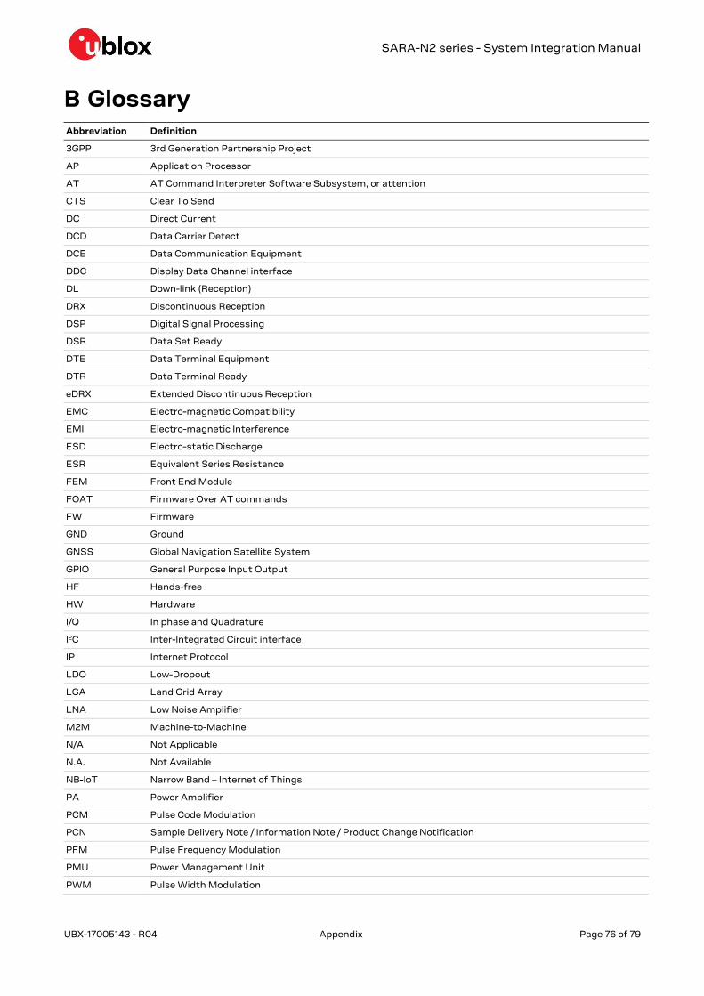
SARA-N2 series - System Integration Manual
UBX-17005143 - R04 Appendix Page 76 of 79
B Glossary Abbreviation Definition
3GPP 3rd Generation Partnership Project
AP Application Processor
AT AT Command Interpreter Software Subsystem, or attention
CTS Clear To Send
DC Direct Current
DCD Data Carrier Detect
DCE Data Communication Equipment
DDC Display Data Channel interface
DL Down-link (Reception)
DRX Discontinuous Reception
DSP Digital Signal Processing
DSR Data Set Ready
DTE Data Terminal Equipment
DTR Data Terminal Ready
eDRX Extended Discontinuous Reception
EMC Electro-magnetic Compatibility
EMI Electro-magnetic Interference
ESD Electro-static Discharge
ESR Equivalent Series Resistance
FEM Front End Module
FOAT Firmware Over AT commands
FW Firmware
GND Ground
GNSS Global Navigation Satellite System
GPIO General Purpose Input Output
HF Hands-free
HW Hardware
I/Q In phase and Quadrature
I2C Inter-Integrated Circuit interface
IP Internet Protocol
LDO Low-Dropout
LGA Land Grid Array
LNA Low Noise Amplifier
M2M Machine-to-Machine
N/A Not Applicable
N.A. Not Available
NB-IoT Narrow Band – Internet of Things
PA Power Amplifier
PCM Pulse Code Modulation
PCN Sample Delivery Note / Information Note / Product Change Notification
PFM Pulse Frequency Modulation
PMU Power Management Unit
PWM Pulse Width Modulation

SARA-N2 series - System Integration Manual
UBX-17005143 - R04 Appendix Page 77 of 79
Abbreviation Definition
RF Radio Frequency
RI Ring Indicator
RRC Radio Resource Control
RTC Real Time Clock
RTS Request To Send
SAW Surface Acoustic Wave
SIM Subscriber Identification Module
TBD To Be Defined
TP Test-Point
UART Universal Asynchronous Receiver-Transmitter
UDP User Datagram Protocol
UICC Universal Integrated Circuit Card
UL Up-link (Transmission)
VSWR Voltage Standing Wave Ratio
Table 31: Explanation of the abbreviations and terms used

SARA-N2 series - System Integration Manual
UBX-17005143 - R04 Related documents Page 78 of 79
Related documents [1] u-blox SARA-N2 series Data Sheet, Docu No UBX-15025564
[2] u-blox Package Information Guide, Docu No UBX-14001652
[3] u-blox SARA-N2 series AT Commands Manual, Docu No UBX-16014887
[4] u-blox NB-IoT Application Development Guide, Docu No UBX-16017368
[5] ITU-T Recommendation V.24 - 02-2000 - List of definitions for interchange circuits between the
Data Terminal Equipment (DTE) and the Data Circuit-terminating Equipment (DCE).
http://www.itu.int/rec/T-REC-V.24-200002-I/en
[6] I2C-bus specification and user manual - Rev. 5 - 9 October 2012 - NXP Semiconductors,
http://www.nxp.com/documents/user_manual/UM10204.pdf
[7] u-blox Nested Design Application Note, Docu No UBX-16007243
[8] u-blox SARA-G3 series Data Sheet, Docu No UBX-13000993
[9] u-blox SARA-U2 series Data Sheet, Docu No UBX-13005287
[10] u-blox SARA-G3 / SARA-U2 series System Integration Manual Docu No UBX-13000995
[11] u-blox AT Commands Manual, Docu No UBX-13002752
[12] u-blox SARA-R4 series Data Sheet, u-blox Document UBX-16024152
[13] u-blox SARA-R4 series System Integration Manual, Docu No UBX-16029218
[14] u-blox SARA-R4 series AT Commands Manual, Docu No UBX-17003787
[15] IEC 60079-0 - Explosive atmospheres, Part 0: Equipment general requirements
[16] IEC 60079-11 - Explosive atmospheres, Part 11: Equipment protection by intrinsic safety “i”
[17] IEC 60079-26 - Explosive atmospheres, Part 26: Equipment with EPL Ga
For regular updates to u-blox documentation and to receive product change notifications, register
on our homepage (www.u-blox.com).
Revision history Revision Date Name Status / Comments
R01 06-Jun-2017 sfal / sses Initial release
R02 31-Oct-2017 sses Updated VCC, V_INT, Power-on, Reset, Antenna Detection, CTS and GPIO
description.
Updated main certification approvals.
R03 22-Feb-2018 sses Extended document applicability to SARA-N211-02X and updated product
status
Updated VCC and switch-on info.
Updated Antenna Detection, CTS and GPIO features info.
Updated approvals info.
Additional design-in examples, minor corrections and improvements.
R04 22-Jun-2018 sses Extended the document applicability to SARA-N201-02B-01.
Updated SARA-N211-02X product status.
Added ATEX and approvals info.
Updated TXD info.
Minor corrections and clarifications.
SARA-N2 series - System Integration Manual
UBX-17005143 - R04 Contact Page 79 of 79
Contact For complete contact information, visit us at www.u-blox.com.
u-blox Offices
North, Central and South America
u-blox America, Inc.
Phone: +1 703 483 3180
E-mail: [email protected]
Regional Office West Coast:
Phone: +1 408 573 3640
E-mail: [email protected]
Technical Support:
Phone: +1 703 483 3185
E-mail: [email protected]
Headquarters
Europe, Middle East, Africa
u-blox AG
Phone: +41 44 722 74 44
E-mail: [email protected]
Support: [email protected]
Asia, Australia, Pacific
u-blox Singapore Pte. Ltd.
Phone: +65 6734 3811
E-mail: [email protected]
Support: [email protected]
Regional Office Australia:
Phone: +61 2 8448 2016
E-mail: [email protected]
Support: [email protected]
Regional Office China (Beijing):
Phone: +86 10 68 133 545
E-mail: [email protected]
Support: [email protected]
Regional Office China (Chongqing):
Phone: +86 23 6815 1588
E-mail: [email protected]
Support: [email protected]
Regional Office China (Shanghai):
Phone: +86 21 6090 4832
E-mail: [email protected]
Support: [email protected]
Regional Office China (Shenzhen):
Phone: +86 755 8627 1083
E-mail: [email protected]
Support: [email protected]
Regional Office India:
Phone: +91 80 405 092 00
E-mail: [email protected]
Support: [email protected]
Regional Office Japan (Osaka):
Phone: +81 6 6941 3660
E-mail: [email protected]
Support: [email protected]
Regional Office Japan (Tokyo):
Phone: +81 3 5775 3850
E-mail: [email protected]
Support: [email protected]
Regional Office Korea:
Phone: +82 2 542 0861
E-mail: [email protected]
Support: [email protected]
Regional Office Taiwan:
Phone: +886 2 2657 1090
E-mail: [email protected]
Support: [email protected]