bg96 lte cat m1/nb1 - home - 5g hub
TRANSCRIPT
1 BG96 miniPCIe Rev 1.0 Copyright © 5GHUB.US
BG96 LTE CAT M1/NB1 BG96 MiniPCIe LTE CAT M1/NB1 Technical Specifications & User Manual
2 BG96 miniPCIe Rev 1.0 Copyright © 5GHUB.US
Purpose of the Document
The purpose of this document is to explain the technical specifications and manual for using the miniPCIe BG96 LTE Cat NB1 module.
Document History
Version Author Date Description A 5G HUB 09.19.2020 Initial Document
3 BG96 miniPCIe Rev 1.0 Copyright © 5GHUB.US
Table of Contents Purpose of the Document .................................................................................................................... 2
Document History ................................................................................................................................ 2
1 Package Content ...................................................................................................................... 4
2 General Description ................................................................................................................. 5 2.1 Overview .................................................................................................................................. 5
2.2 Key Features ............................................................................................................................. 5
2.3 Data Rate .................................................................................................................................. 5
2.4 Interfaces ................................................................................................................................. 5
2.5 Software Features .................................................................................................................... 5
2.6 Protocols .................................................................................................................................. 6
2.7 General Features ...................................................................................................................... 6
2.8 Approvals ................................................................................................................................. 6
2.9 Overview Diagrams .................................................................................................................. 6
2.10 Functional Diagram ................................................................................................................. 7
2.11 MiniPCIe Pin Diagram and Assignment ................................................................................... 8
2.12 Pin Description ........................................................................................................................ 9
2.13 Operating Models ................................................................................................................. 10
2.14 Power Saving ......................................................................................................................... 11
2.14.1 Sleep Mode ................................................................................................................... 11
2.15 Airplane Mode ...................................................................................................................... 11
2.16 W_DISABLE# .......................................................................................................................... 11
2.17 PERST# ................................................................................................................................... 12
2.18 LED_WWAN# ........................................................................................................................ 12
2.19 WAKE# ................................................................................................................................... 12
4 BG96 miniPCIe Rev 1.0 Copyright © 5GHUB.US
1 Package Content
Package:
• miniPCIe for BG96.
Download software:
Software can be downloaded from the following website:
https://www.5ghub.us/download
Software to download:
• QNavigatorV1.6 (in the folder \Tools). • Quectel driver (in the folder \Driver).
Documentation:
• Quectel AT commands and GNSS commands manual (in the folder \Doc).
5 BG96 miniPCIe Rev 1.0 Copyright © 5GHUB.US
2 General Description 2.1 Overview BG96 Mini PCIe is a series of LTE category M1/NB1 module adopting standard PCI Express Mini Card form factor (Mini PCIe). It is optimized specially for M2M and IoT applications and delivers 150Mbps downlink and 50Mbps uplink data rates. It provides data connectivity on LTE-TDD/LTE-FDD/GPRS/EGPRS networks, and supports half-duplex operation in LTE networks.
BG96 provides GNSS functionality to meet customers and supports Qualcomm® location technology (GPS, GLONASS, BeiDou, Galileo and QZSS). The integrated GNSS greatly simplifies product design, and provides quicker, more accurate and more dependable positioning.
A rich set of Internet protocols, industry-standard interfaces, and abundant functionalities (USB serial drivers for Windows 7/8/8.1/10, Linux, Android) extend the applicability of the module to a wide range of M2M applications such as industrial router, industrial PDA, rugged tablet PC, video surveillance and digital signage.
2.2 Key Features • LTE category M1/NB1 module optimized for broadband IoT applications • Worldwide LTE, and GSM/GPRS/EDGE coverage • Standard PCI Express® MiniCard form factor (Mini PCIe) ideal for manufacturers to easily
integrate wireless connectivity into their devices • GNSS Gen8C Lite of Qualcomm. Multi-constellation GNSS receiver available for applications
requiring fast and accurate fixes in any environment • LTE FDD: B1/B2/B3/B4/B5/B8/B12/B13/B18/B19/B20/B25/B26*/B28 • LTE-TDD: B39 (for Cat M1 only) • GSM 850/EGSM 900/DCS 1800/PCS 1900
2.3 Data Rate • LTE
Cat M1: Max. 375Kbps (DL)/375Kbps (UL) Cat NB1: Max. 32Kbps (DL)/70Kbps (UL)
• GPRS: Max. 107Kbps (DL)/85.6Kbps (UL)
• EDGE: Max. 296Kbps (DL)/236.8Kbps (UL)
2.4 Interfaces • USB 2.0 with High Speed up to 480Mbps • 1.8V/3.0V (U)SIM Interface • NETLIGHT LED for network connectivity status indication • UART × 3 • One main antenna (ANT_MAIN) and one GNSS antenna (ANT_GNSS) interfaces
2.5 Software Features • USB Serial Driver:
Windows 7/8/8.1/10, Linux 3.x(3.4 or later)/4.1~4.15 Android 4.x/5.x/6.x/7.x/8.x/9.x
6 BG96 miniPCIe Rev 1.0 Copyright © 5GHUB.US
2.6 Protocols • Support PPP/TCP/UDP/SSL/TLS/FTP(S)/HTTP(S)/NITZ/PING/MQTT protocols. Support PAP
(Password Authentication Protocol) and CHAP (Challenge Handshake Authentication Protocol) protocols which are usually used for PPP connections
2.7 General Features • Temperature Range: -35°C ~ +75°C • Dimensions: 30.0mm x 51.0mm x 4.9mm • Weight: Approx. 9.8g • Mini PCIe Package • Supply Voltage: 3.0V~3.6V, 3.3V Typ. • 3GPP E-UTRA Release 12 • Bandwidth: 1.4/3/5/10/15/20MHz • 3GPP TS 27.007
2.8 Approvals
• Carrier: Vodafone (Global) Deutsche Telekom/Telefónica (Europe) Verizon/AT&T/T-Mobile/U.S. Cellular (North America) Rogers/Bell*/Telus* (Canada) SKT/KT*/LGU+* (South Korea) NTT DOCOMO/SoftBank/KDDI (Japan)
• Regulatory: GCF (Global) CE (Europe) FCC/PTCRB (North America) IC (Canada) Anatel (Brazil) KC (South Korea) NCC (Taiwan) JATE/TELEC (Japan) RCM (Australia/New Zealand) FAC (Russia) NBTC (Thailand) ICASA (South Africa)
• Others: RoHS Compliant WHQL
2.9 Overview Diagrams
7 BG96 miniPCIe Rev 1.0 Copyright © 5GHUB.US
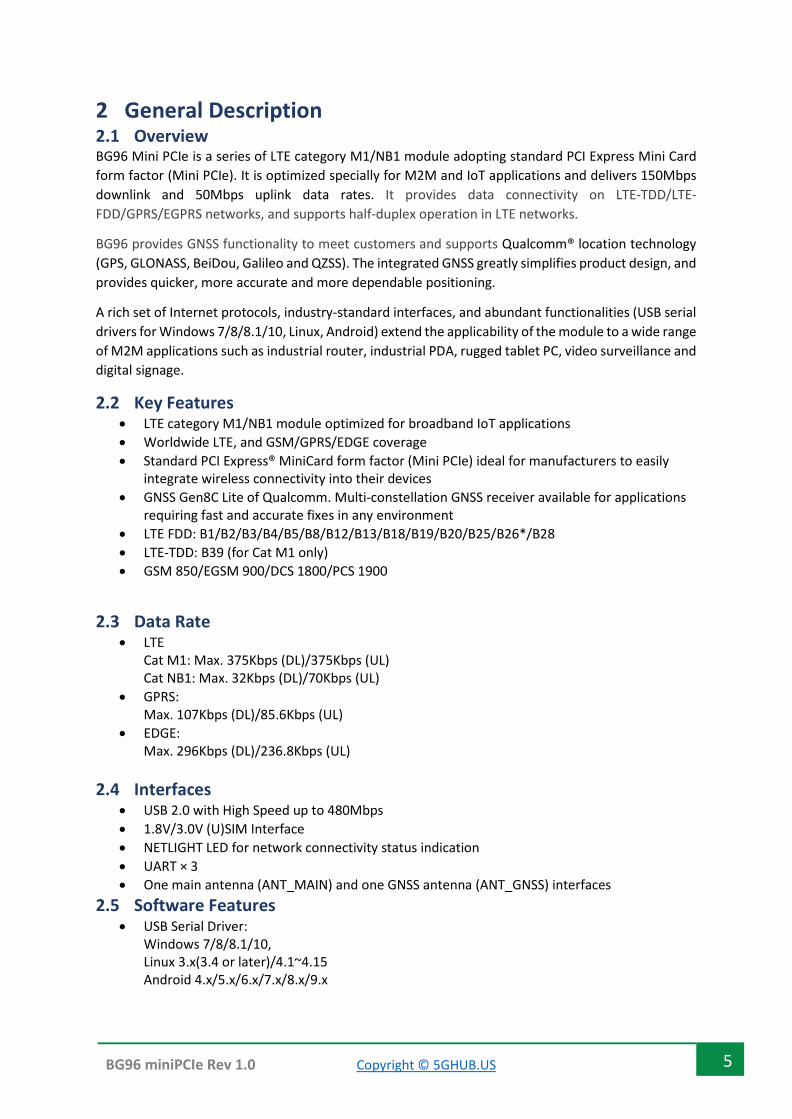
Figure 1. BG96 miniPCIe LTE Cat M1/NB1 module.
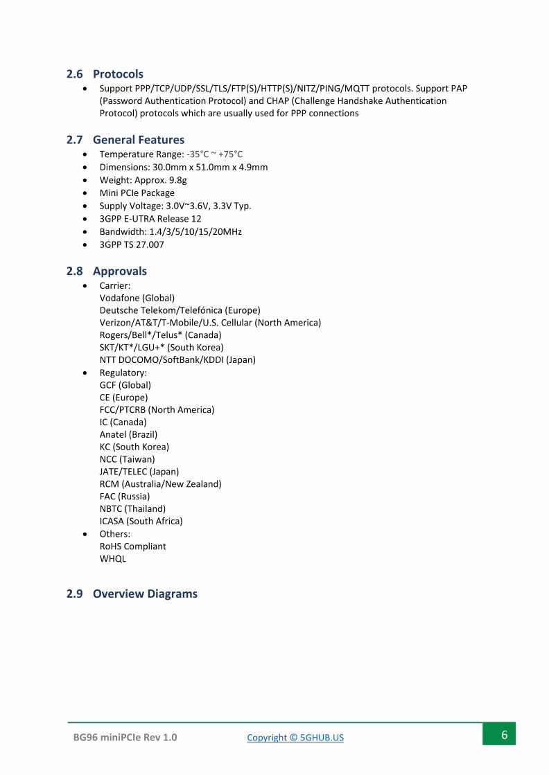
2.10 Functional Diagram The following figure shows the block diagram of BG96 miniPCIe.
8 BG96 miniPCIe Rev 1.0 Copyright © 5GHUB.US
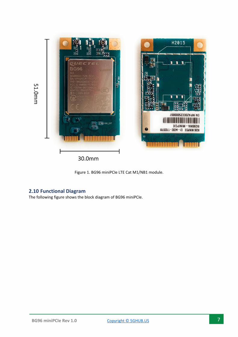
Figure 2. Physical characteristics.
2.11 MiniPCIe Pin Diagram and Assignment The physical connections and signal levels of BG96 Mini PCIe comply with PCI Express Mini Card Electromechanical Specification.
• Power supply • (U)SIM interface • USB interface • UART interfaces • PCM and I2C interfaces • Control and indication pins

9 BG96 miniPCIe Rev 1.0 Copyright © 5GHUB.US
Figure 3. BG96 miniPCIe pin assignment
2.12 Pin Description
Pin # Pin Name Pin Direction Pin Functionality 1 NC 2 VCC_3V3 I 3.0V~3.6V, typically
3.3V DC supply 3 NC 4 GND Mini card ground 5 NC 6 NC Not connected 7 RESERVED Reserved 8 USIM_VDD O Power supply for the
(U)SIM card 9 GND
10 USIM_DATA I Data signal of (U)SIM card
11 UART_RX I UART receive data 12 USIM_CLK O Clock signal of (U)SIM
card 13 UART_TX O UART transmit data 14 USIM_RST O Reset signal of (U)SIM
card 15 GND 16 RESERVED 17 RI O Ring indication 18 GND 19 RESERVED

10 BG96 miniPCIe Rev 1.0 Copyright © 5GHUB.US
20 W_DISABLE# I Airplane mode control 21 GND 22 PERST# I Fundamental reset
signal 23 UART_CTS I UART clear to send 24 RESERVED 25 UART_RTS O UART request to send 26 GND 27 GND 28 NC 29 GND 30 I2C_SCL OD I2C serial clock 31 DTR DI Sleep mode control 32 I2C_SDA OD OD I2C serial data 33 RESERVED 34 GND 35 GND 36 USB_DM IO USB differential data (-) 37 GND 38 USB_DP IO USB differential data (+) 39 VCC_3V3 I 3.0V~3.6V, typically
3.3V DC supply 40 GND 41 VCC_3V3 I 3.0V~3.6V, typically
3.3V DC supply 42
LED_WWAN# OC LED signal for indicating
the network status of the module
43 GND 44 NC (U)SIM card insertion
detection 45 PCM_CLK IO PCM clock signal 46 RESERVED 47 PCM_DOUT O PCM data output 48 NC 49 PCM_DIN I PCM data input 50 GND 51 PCM_SYNC IO PCM frame
synchronization 52 VCC_3V3 PI 3.0V~3.6V, typically
3.3V DC supply
2.13 Operating Models The following table outlines the operating modes to be mentioned in the following chapters.
Mode Detail Normal Operation Idle Software is active. The module has registered on
the network, and it is ready to send and receive data

11 BG96 miniPCIe Rev 1.0 Copyright © 5GHUB.US
Talk/Data Network connection is ongoing. In this mode, the power consumption is decided by network setting and data transfer rate.
Minimum Functionality Mode AT+CFUN command can set the module to a minimum functionality mode without removing the power supply. In this case, both RF function and (U)SIM card will be invalid.
Airplane Mode AT+CFUN command or W_DISABLE# pin can set the module to airplane mode. In this case, RF function will be invalid.
Sleep Mode In this mode, the current consumption of the module will be reduced to the minimal level. In this mode, the module can still receive paging message, SMS, voice call and TCP/UDP data from the network normally
2.14 Power Saving 2.14.1 Sleep Mode BG96 Mini PCIe can reduce its current consumption to a minimum value in sleep mode. There are three preconditions must be met to make the module enter sleep mode.
• Execute AT+QSCLK=1 to enable sleep mode • Ensure the DTR is kept at high level or be kept open • The host’s USB bus, which is connected with the module’s USB interface, enters suspend state
2.15 Airplane Mode When the module enters airplane mode, the RF function will be disabled, and all AT commands related to it will be inaccessible.
2.16 W_DISABLE# W_DISABLE# enables/disables the RF function (excluding GNSS). It is pulled up by default, and driving it low makes the module enter airplane mode. The pin function is disabled by default, and AT+QCFG="airplanecontrol",1 can be used to enable this function.
Airplane Mode Control (Hardware Method)
W_DISABLE# RF Function Status Module Operation Mode
High level (default) RF enabled Normal mode
Low level RF disabled Airplane mode
The RF function can also be enabled/disabled with AT+CFUN=<fun>, and the details are listed below.
12 BG96 miniPCIe Rev 1.0 Copyright © 5GHUB.US
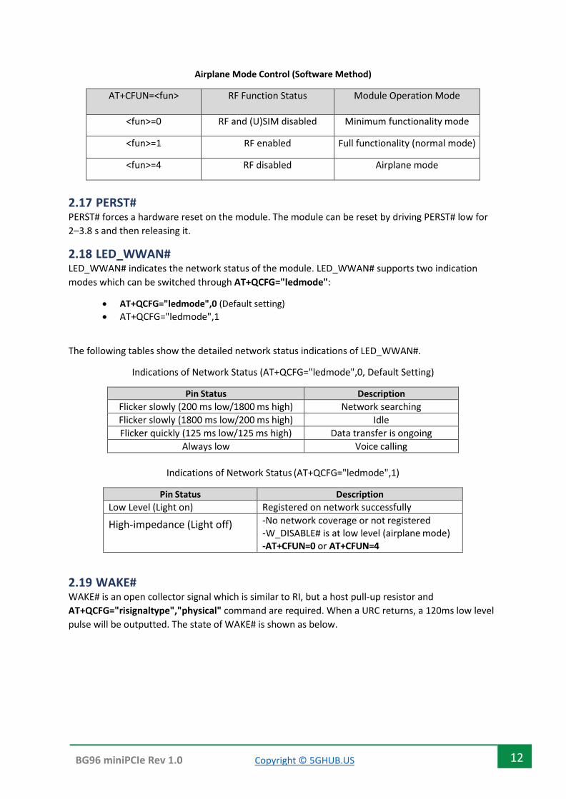
Airplane Mode Control (Software Method)
AT+CFUN=<fun> RF Function Status Module Operation Mode
<fun>=0 RF and (U)SIM disabled Minimum functionality mode
<fun>=1 RF enabled Full functionality (normal mode)
<fun>=4 RF disabled Airplane mode
2.17 PERST# PERST# forces a hardware reset on the module. The module can be reset by driving PERST# low for 2–3.8 s and then releasing it.
2.18 LED_WWAN# LED_WWAN# indicates the network status of the module. LED_WWAN# supports two indication modes which can be switched through AT+QCFG="ledmode":
• AT+QCFG="ledmode",0 (Default setting) • AT+QCFG="ledmode",1
The following tables show the detailed network status indications of LED_WWAN#.
Indications of Network Status (AT+QCFG="ledmode",0, Default Setting)
Pin Status Description Flicker slowly (200 ms low/1800 ms high) Network searching Flicker slowly (1800 ms low/200 ms high) Idle Flicker quickly (125 ms low/125 ms high) Data transfer is ongoing
Always low Voice calling
Indications of Network Status (AT+QCFG="ledmode",1)
Pin Status Description Low Level (Light on) Registered on network successfully
High-impedance (Light off)
-No network coverage or not registered -W_DISABLE# is at low level (airplane mode) -AT+CFUN=0 or AT+CFUN=4
2.19 WAKE# WAKE# is an open collector signal which is similar to RI, but a host pull-up resistor and AT+QCFG="risignaltype","physical" command are required. When a URC returns, a 120ms low level pulse will be outputted. The state of WAKE# is shown as below.