real time clock interfacing with fpga
TRANSCRIPT

International Islamic University
Islamabad
FPGA LAB PROJECT
Real Time Clock Interfacing With FPGA
Submitted by:
Mafaz Ahmed 1882-F12D
FPGA LAB PROJECT Page 1
TABLE OF CONTENTS Pages
1. Introduction .…………………………..(1)
2. Real Time Clock RTC module (DS 1307) …………….…….……....(1)
Description
Features
Circuit Diagram
Data Registers
3. I2C protocol …..…………………………………..(5)
Description
Features
Timing Diagram
4. FPGA KIT (SPARTAN 2) ...…………………………………….(6)
Description
Features
5. Schematic ……………………………………….(6)
6. Verilog Code ………..…………………………….(7)
7. Hardware Implementation .…………………………………….(12)
8. Conclusion .…………………………………….(13)
9. References …………………………………….(13)
FPGA LAB PROJECT Page 2

1. Introduction:
A real-time clock (RTC) is a computer clock (most often in the form of an integrated circuit) that keeps track of the current time. Although the term often refers to the devices in personal computers, servers and embedded systems, RTCs are present in almost any electronic device which needs to keep accurate time.
It features the DS1307 serial real-time clock (RTC). It is a low-power, full binary-coded decimal (BCD) clock/calendar with programmable square-wave output signal. Board uses I2C interface for communication, and can only use 5V power supply. Board features a 3V/230mA lithium battery as a backup power supply which ensures that timekeeping operation continues even when the main power supply goes OFF.
2. Real Time Clock RTC module (DS 1307):
Description:
RTC DS 1307 is a great battery-backed real time clock (RTC) that allows your microcontroller project to keep track of time even if it is reprogrammed, or if the power is lost. Perfect for data logging, clock-building, time stamping, timers and alarms, etc. The DS1307 is the most popular RTC,
and works best with 5V-based chips.
FPGA LAB PROJECT Page 3

Features:
Two wire I2C interface Hour : Minutes : Seconds AM/PM Day Month, Date - Year Leap year compensation Accurate calendar up to year 2100 Battery backup included 1Hz output pin 56 Bytes of Non-volatile memory available to user 0x68 I2C Address
Circuit Diagram:
FPGA LAB PROJECT Page 4

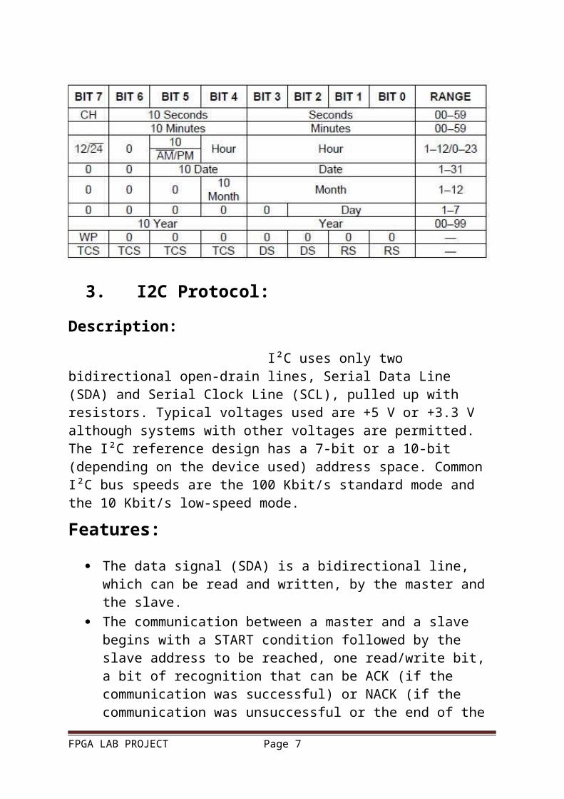
DATA Registers:
3. I2C Protocol:
Description:
I²C uses only two bidirectional open-drain lines, Serial Data Line (SDA) and Serial Clock Line (SCL), pulled up with resistors. Typical voltages used are +5 V or +3.3 V although systems with other voltages are permitted. The I²C reference design has a 7-bit or a 10-bit (depending on the device used) address space. Common I²C bus speeds are the 100 Kbit/s standard mode and the 10 Kbit/s low-speed mode.
Features:
The data signal (SDA) is a bidirectional line, which can be read and written, by the master and the slave.
The communication between a master and a slave begins with a START condition followed by the slave address to be reached, one read/write bit, a bit of recognition that can be ACK (if the communication was successful) or NACK (if the communication was unsuccessful or the end of the message is set by the master), the 8 bits of data to send or to receive, the ACK or NACK bit, and finishes with a STOP condition or a condition Repeated START.
FPGA LAB PROJECT Page 5

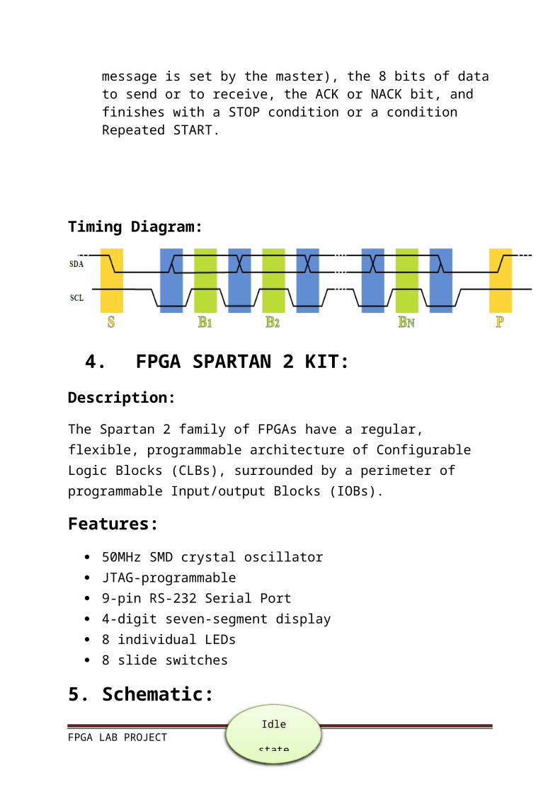
Timing Diagram:
4. FPGA SPARTAN 2 KIT:
Description:
The Spartan 2 family of FPGAs have a regular, flexible, programmable architecture of Configurable Logic Blocks (CLBs), surrounded by a perimeter of programmable Input/output Blocks (IOBs).
Features:
50MHz SMD crystal oscillator JTAG-programmable 9-pin RS-232 Serial Port 4-digit seven-segment display 8 individual LEDs 8 slide switches
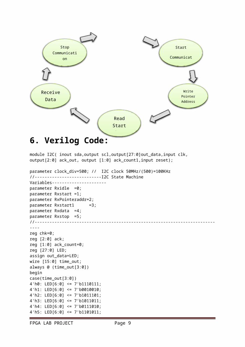
5. Schematic:
FPGA LAB PROJECT Page 6
Idle
stateStart
Communication
Write Pointer Address
Read Start from slave
Stop Communication
Receive Data
6. Verilog Code:module I2C( inout sda,output scl,output[27:0]out_data,input clk, output[2:0] ack_out, output [1:0] ack_count1,input reset);
parameter clock_div=500; // I2C clock 50MHz/(500)=100KHz//---------------------------I2C State Machine Variables----------------------parameter Rxidle =0;parameter Rxstart =1;parameter RxPointeraddr=2;parameter Rxstart1 =3;parameter Rxdata =4;parameter Rxstop =5;//-----------------------------------------------------------------------------reg chk=0;reg [2:0] ack;reg [1:0] ack_count=0;reg [27:0] LED;assign out_data=LED;wire [15:0] time_out;always @ (time_out[3:0])begincase(time_out[3:0])4'h0: LED[6:0] <= 7'b1110111;4'h1: LED[6:0] <= 7'b0010010;4'h2: LED[6:0] <= 7'b1011101;4'h3: LED[6:0] <= 7'b1011011;4'h4: LED[6:0] <= 7'b0111010;4'h5: LED[6:0] <= 7'b1101011;4'h6: LED[6:0] <= 7'b1101111;4'h7: LED[6:0] <= 7'b1010010;4'h8: LED[6:0] <= 7'b1111111;4'h9: LED[6:0] <= 7'b1111010;4'hA: LED[6:0] <= 7'b1111110;4'hB: LED[6:0] <= 7'b1111111;4'hC: LED[6:0] <= 7'b1100101;4'hD: LED[6:0] <= 7'b1110111;4'hE: LED[6:0] <= 7'b1101101;4'hF: LED[6:0] <= 7'b1101100;default:LED[6:0] <= 7'bxxxxxxx;endcaseendalways @ (time_out[7:4])begincase(time_out[7:4])4'h0: LED[13:6] <= 7'b1110111;4'h1: LED[13:6] <= 7'b0010010;4'h2: LED[13:6] <= 7'b1011101;4'h3: LED[13:6] <= 7'b1011011;4'h4: LED[13:6] <= 7'b0111010;4'h5: LED[13:6] <= 7'b1101011;4'h6: LED[13:6] <= 7'b1101111;4'h7: LED[13:6] <= 7'b1010010;4'h8: LED[13:6] <= 7'b1111111;4'h9: LED[13:6] <= 7'b1111010;4'hA: LED[13:6] <= 7'b1111110;
FPGA LAB PROJECT Page 7
4'hB: LED[13:6] <= 7'b1111111;4'hC: LED[13:6] <= 7'b1100101;4'hD: LED[13:6] <= 7'b1110111;4'hE: LED[13:6] <= 7'b1101101;4'hF: LED[13:6] <= 7'b1101100;default:LED[13:6] <= 7'bxxxxxxx;endcaseendalways @ (time_out[11:8])begincase(time_out[11:8])4'h0: LED[20:7] <= 7'b1110111;4'h1: LED[20:7] <= 7'b0010010;4'h2: LED[20:7] <= 7'b1011101;4'h3: LED[20:7] <= 7'b1011011;4'h4: LED[20:7] <= 7'b0111010;4'h5: LED[20:7] <= 7'b1101011;4'h6: LED[20:7] <= 7'b1101111;4'h7: LED[20:7] <= 7'b1010010;4'h8: LED[20:7] <= 7'b1111111;4'h9: LED[20:7] <= 7'b1111010;4'hA: LED[20:7] <= 7'b1111110;4'hB: LED[20:7] <= 7'b1111111;4'hC: LED[20:7] <= 7'b1100101;4'hD: LED[20:7] <= 7'b1110111;4'hE: LED[20:7] <= 7'b1101101;4'hF: LED[20:7] <= 7'b1101100;default:LED[20:7] <= 7'bxxxxxxx;endcaseendalways @ (time_out[15:8])begincase(time_out[15:8])4'h0: LED[27:21] <= 7'b1110111;4'h1: LED[27:21] <= 7'b0010010;4'h2: LED[27:21] <= 7'b1011101;4'h3: LED[27:21] <= 7'b1011011;4'h4: LED[27:21] <= 7'b0111010;4'h5: LED[27:21] <= 7'b1101011;4'h6: LED[27:21] <= 7'b1101111;4'h7: LED[27:21] <= 7'b1010010;4'h8: LED[27:21] <= 7'b1111111;4'h9: LED[27:21] <= 7'b1111010;4'hA: LED[27:21] <= 7'b1111110;4'hB: LED[27:21] <= 7'b1111111;4'hC: LED[27:21] <= 7'b1100101;4'hD: LED[27:21] <= 7'b1110111;4'hE: LED[27:21] <= 7'b1101101;4'hF: LED[27:21] <= 7'b1101100;default:LED[27:21] <= 7'bxxxxxxx;endcaseend//------------------------------------------------------------------------------reg I2Cclk =1; // I2C clock reg [8:0] clkclk=clock_div; // in order to divide 50MHz clock reg sda_int =1; // making SDA high in initial statereg [15:0] outreg =0;
FPGA LAB PROJECT Page 8
reg [3:0] I2C_counter=0; // for giving the pointer address reg [3:0] bitaddrs7=4'b0001; // initializing via giving slave address(1001000-0(R/W))reg [3:0] Rxcount=0;reg [3:0] slaveaddrs=0; //receiving data from ds1307/// ----------------------------------------------------------------------------
reg [2:0] state =Rxidle ; // For State machine startingassign scl =chk?1'b1:I2Cclk;// Generated Clock for I2Cassign time_out = outreg; // output from ds1307assign sda =sda_int; // Using SDA pinassign ack_out=ack;assign ack_count1=ack_count;
////------------------------------always @ (posedge clk) /// --------------------- scl generation-----------------begin
clkclk=clkclk - 1; if(clkclk==0)beginI2Cclk=~I2Cclk;clkclk =clock_div;end
end////.............................................................................always @(posedge I2Cclk )if(reset)begin chk <=1; outreg <=0; I2C_counter <=0; bitaddrs7 <=4'b0001; Rxcount <=0; slaveaddrs <=0; ack <=0; ack_count <=0; I2Cclk <=1; sda_int <=1; clkclk <=clock_div;end
always @(posedge I2Cclk )begin
////....................................state machine............................ case (state)//-------------------------------------------------------------------------------Rxidle:
begin sda_int=1'b0; //---------------------start sda = 0
chk=1'b0; //---------------------start scl
state =Rxstart;end//-------------------------------------------------------------------------------Rxstart:begin
case(bitaddrs7)// initial frame 1101000 Initializing slave address ds1307
FPGA LAB PROJECT Page 9

1: begin sda_int =1'b1;//---------------------sda 1bitaddrs7=bitaddrs7+1; end
2: begin sda_int =1'b1;//---------------------sda 1bitaddrs7=bitaddrs7+1; end
3: begin sda_int =1'b0;//---------------------sda 0bitaddrs7=bitaddrs7+1; end
4: begin sda_int =1'b1;//---------------------sda 1bitaddrs7=bitaddrs7+1; end
5: begin sda_int =1'b0;//---------------------sda 0bitaddrs7=bitaddrs7+1; end
6: begin sda_int =1'b0;//---------------------sda 0bitaddrs7=bitaddrs7+1; end
7: begin sda_int =1'b0;//---------------------sda=0 bitaddrs7=bitaddrs7+1; end
8: begin sda_int =1'b0;ack_count=2'b00; bitaddrs7=bitaddrs7+1; // R/W bit
end9: begin if(sda==1'b0)
ack[0]=1;state=RxPointeraddr; // Checking ack end
endcaseend//---------------------------------------------------------------------------------RxPointeraddr:
// Pointer Address 00000001 for minute registerbegin
case(I2C_counter)//---------------------sda = 0
0: begin sda_int =1'b0;I2C_counter=I2C_counter+1;end
//---------------------sda = 01: begin sda_int =1'b0;
I2C_counter=I2C_counter+1;end//---------------------sda = 0
2: begin sda_int =1'b0;I2C_counter=I2C_counter+1; end
//---------------------sda = 03: begin sda_int =1'b0;
I2C_counter=I2C_counter+1; end//---------------------sda = 0
4: begin sda_int =1'b0;I2C_counter=I2C_counter+1;end
//---------------------sda = 05: begin sda_int =1'b0;
I2C_counter=I2C_counter+1;end//---------------------sda = 0
FPGA LAB PROJECT Page 10

6: begin sda_int =1'b0;I2C_counter=I2C_counter+1;end
//---------------------sda = 17: begin sda_int =1'b0;
ack_count=2'b01; I2C_counter=I2C_counter+1;end
8: begin if(sda==1'b0) ack[1]=1'b0; state=Rxstart1;end // after pointer register sda line
acknoledged by a low pulseendcase
end //-----------------------------------start+ slave address byte---------------------Rxstart1:begin
case(slaveaddrs)// initial frame 1101000 Initializing slave address including start (case 0:)
0: begin sda_int=1'b0; slaveaddrs=slaveaddrs+1; end
1: begin sda_int =1'b1;//---------------------sda 1slaveaddrs=slaveaddrs+1; end
2: begin sda_int =1'b1;//---------------------sda 1slaveaddrs=slaveaddrs+1; end
3: begin sda_int =1'b0;//---------------------sda 0slaveaddrs=slaveaddrs+1; end
4: begin sda_int =1'b1;//---------------------sda 1slaveaddrs=slaveaddrs+1; end
5: begin sda_int =1'b0;//---------------------sda 0slaveaddrs=slaveaddrs+1; end
6: begin sda_int =1'b0;//---------------------sda 0slaveaddrs=slaveaddrs+1; end
7: begin sda_int =1'b0;//---------------------sda=0 slaveaddrs=slaveaddrs+1; end
8: begin sda_int =1'b1;slaveaddrs=slaveaddrs+1; // R/W bit highack_count=2'b10; end
9: begin if(sda==1'b0)ack[2]=1;state=Rxdata; // Checking ack end
endcaseend
//----------------------------------receiving time --------------------------Rxdata:begin
case(Rxcount)0: begin outreg[15]=sda;
FPGA LAB PROJECT Page 11

Rxcount=Rxcount+1;end1: begin outreg[14]=sda;
Rxcount=Rxcount+1;end2: begin outreg[13]=sda;
Rxcount=Rxcount+1;end3: begin outreg[12]=sda;
Rxcount=Rxcount+1;end4: begin outreg[11]=sda;
Rxcount=Rxcount+1;end5: begin outreg[10]=sda;
Rxcount=Rxcount+1;end6: begin outreg[9]=sda;
Rxcount=Rxcount+1;end7: begin outreg[8]=sda;
Rxcount=Rxcount+1;ack_count=2'b11; end
// low pulse acknoledgment from ds13078: begin outreg[7]=sda;
if(!sda) ack[2]=1;Rxcount=Rxcount+1;end
9: begin outreg[6]=sda ;Rxcount=Rxcount+1;end
10: begin outreg[5]=sda ;Rxcount=Rxcount+1;end
11: begin outreg[4]=sda;Rxcount=Rxcount+1;end
12: begin outreg[3]=sda;Rxcount=Rxcount+1;end
13: begin outreg[2]=sda;Rxcount=Rxcount+1;end
14: begin outreg[1]=sda;Rxcount=Rxcount+1;end
15: begin sda_int=1'b0; // checking low pulse acknoledge frm ds1307state=Rxstop; end endcase
end//-----------------------------------------------------------------------------------------Rxstop:begin chk=1; sda_int=1'b1; state= Rxidle; end
endcaseendendmodule
FPGA LAB PROJECT Page 12

Hardware Implementation:
RTC is connected to Spartan 2 kit and the result will be shown on seven segments and LED’s. Acknowledgements will be shown on LED’s and Receive data will be shown on seven segments.
Conclusion:
We have interface RTC with FPGA kit using I2C protocol. They are interface by using SCL and SDA lines. As FPGA have limited input/output pins so we cannot interface parallel RTC, so the best way to interface RTC is to use I2C protocol with only 2 wires.
References:https://www.sparkfun.com/products/12708
http://www.instructables.com/id/Real-Time-Clock-DS1302/
http://en.wikipedia.org/wiki/I%C2%B2C
http://www.digikey.com/catalog/en/partgroup/spartan-ii/14470
FPGA LAB PROJECT Page 13