hardware interfacing supplying clock & power buses and bridges dc/ac analysis timing...
TRANSCRIPT
Hardware interfacing
Supplying Clock & Power Buses and bridges DC/AC analysis Timing analysis Design considerations Design for worst case
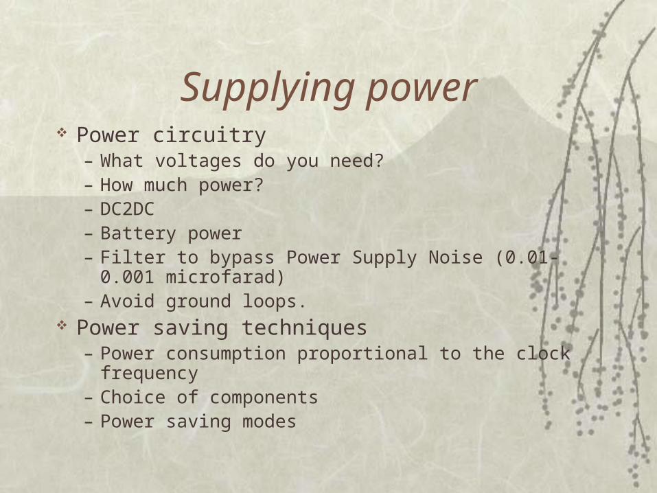
Supplying power Power circuitry
– What voltages do you need?– How much power?– DC2DC– Battery power– Filter to bypass Power Supply Noise (0.01-0.001 microfarad) – Avoid ground loops.
Power saving techniques– Power consumption proportional to the clock frequency– Choice of components– Power saving modes
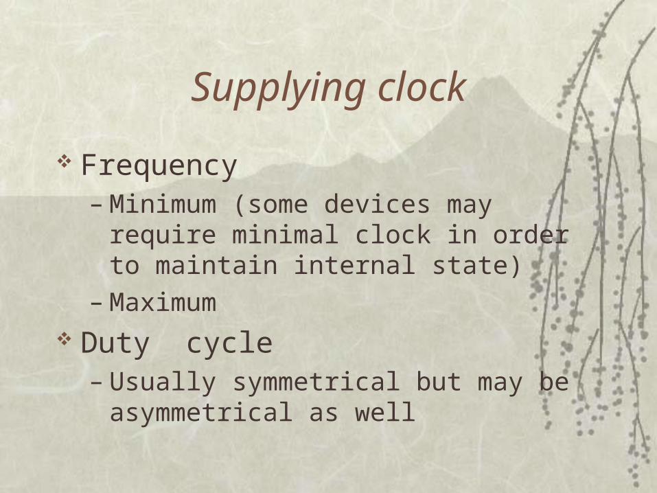
Supplying clock
Frequency– Minimum (some devices may require minimal
clock in order to maintain internal state)– Maximum
Duty cycle– Usually symmetrical but may be asymmetrical
as well
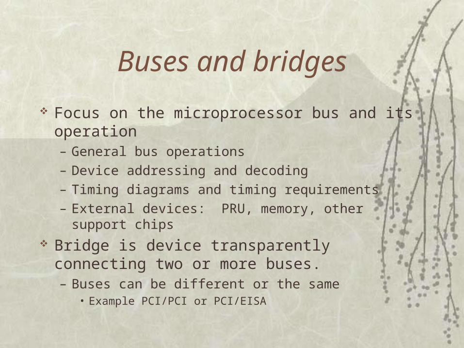
Buses and bridges
Focus on the microprocessor bus and its operation– General bus operations
– Device addressing and decoding
– Timing diagrams and timing requirements
– External devices: PRU, memory, other support chips Bridge is device transparently connecting two or
more buses.– Buses can be different or the same
• Example PCI/PCI or PCI/EISA
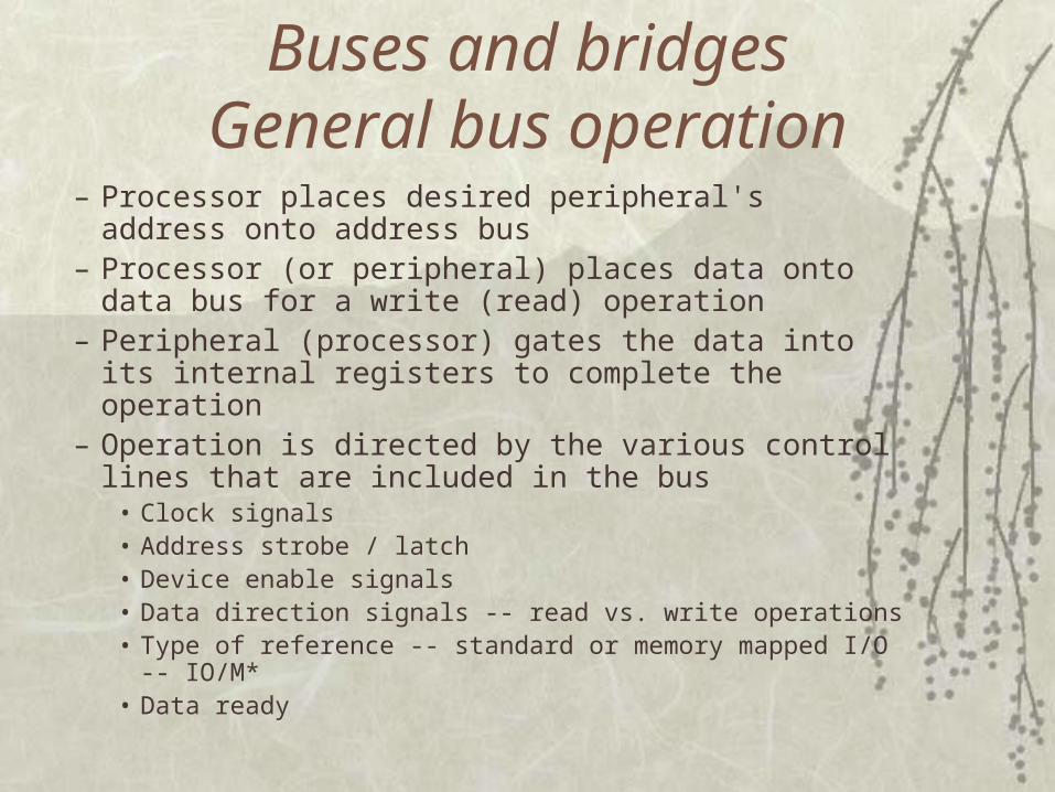
Buses and bridgesGeneral bus operation
– Processor places desired peripheral's address onto address bus
– Processor (or peripheral) places data onto data bus for a write (read) operation
– Peripheral (processor) gates the data into its internal registers to complete the operation
– Operation is directed by the various control lines that are included in the bus
• Clock signals• Address strobe / latch• Device enable signals• Data direction signals -- read vs. write operations• Type of reference -- standard or memory mapped I/O -- IO/M*• Data ready
Timing analysis
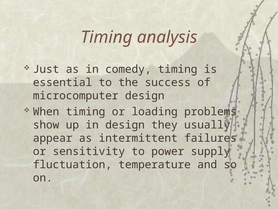
Just as in comedy, timing is essential to the success of microcomputer design
When timing or loading problems show up in design they usually appear as intermittent failures or sensitivity to power supply fluctuation, temperature and so on.
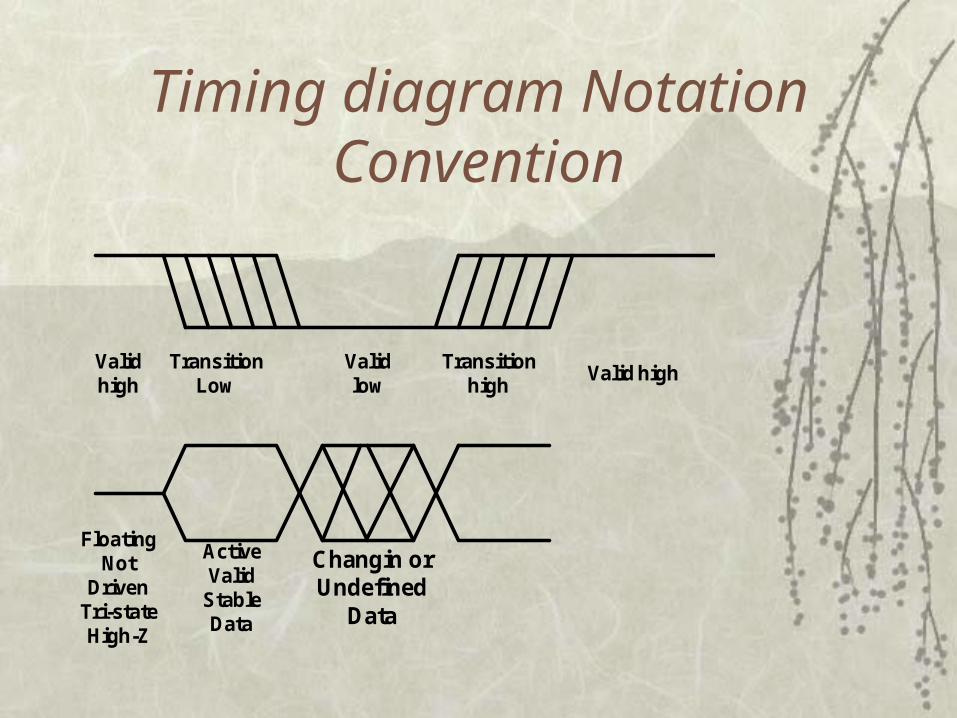
Timing diagram Notation Convention
Validhigh
TransitionLow
Validlow
Transitionhigh
Valid high
FloatingNot
DrivenTri-stateHigh-Z
ActiveValid
StableData
Changin orUndefined
Data
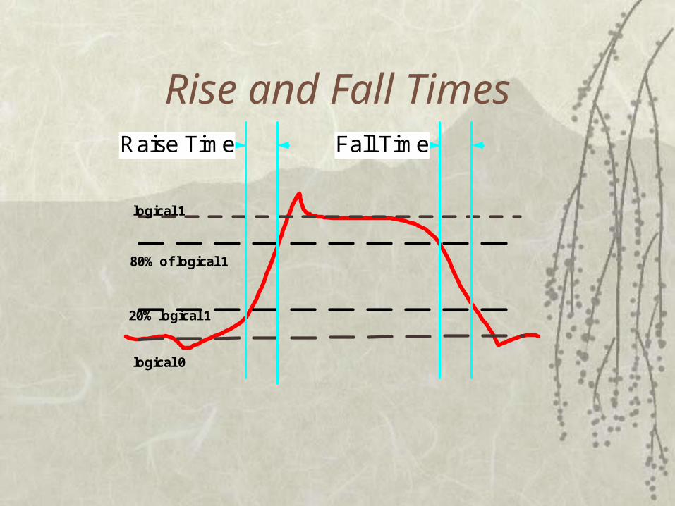
Rise and Fall Times
20% logical 1
logical 1
80% of logical 1
logical 0
Raise Time Fall Time
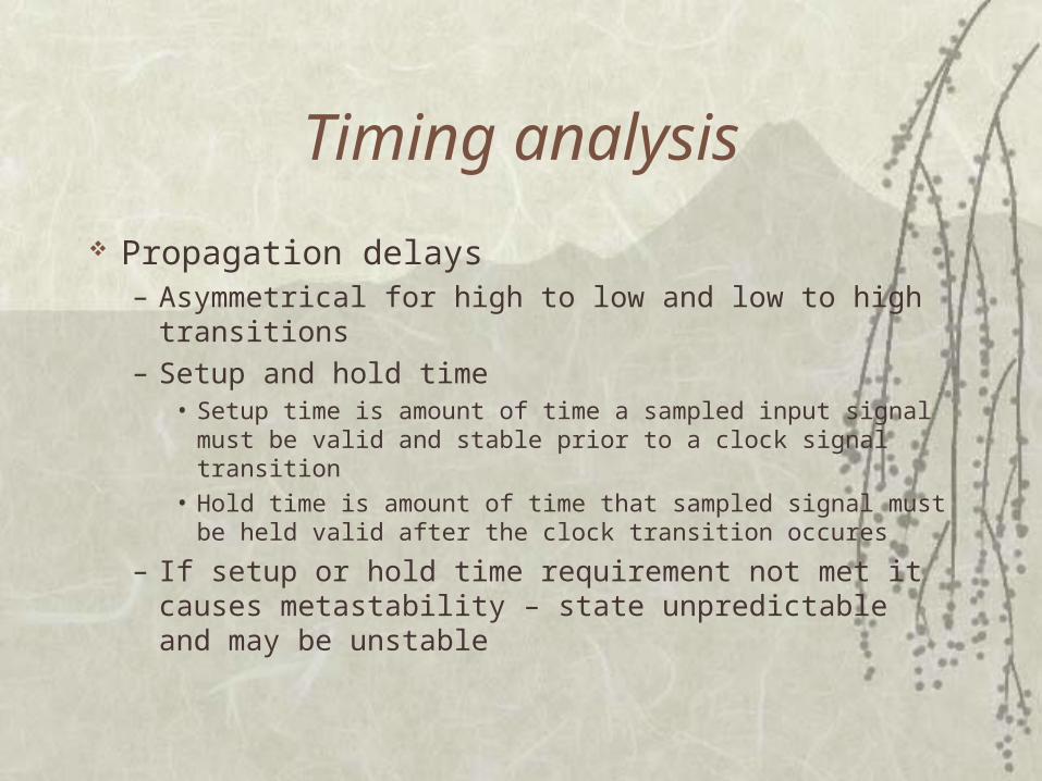
Timing analysis
Propagation delays– Asymmetrical for high to low and low to high
transitions
– Setup and hold time• Setup time is amount of time a sampled input signal must be
valid and stable prior to a clock signal transition
• Hold time is amount of time that sampled signal must be held valid after the clock transition occures
– If setup or hold time requirement not met it causes metastability – state unpredictable and may be unstable
Timing diagrams
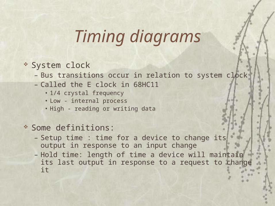
System clock– Bus transitions occur in relation to system clock– Called the E clock in 68HC11
• 1/4 crystal frequency• Low - internal process• High - reading or writing data
Some definitions:– Setup time : time for a device to change its output in
response to an input change– Hold time: length of time a device will maintain its last
output in response to a request to change it
Example
Fan-Out and Loading analysis DC and AC
The main question can this output drive all the inputs I want connect to it?
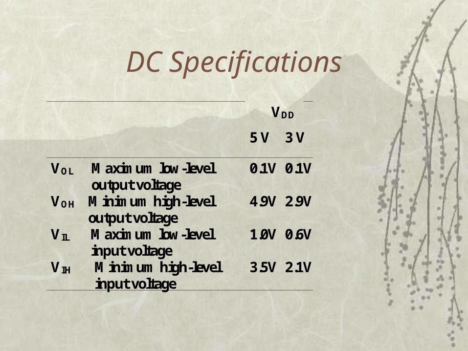
DC Specifications
VDD
5 V 3 V
VOL Maximum low-level output voltage
0.1V 0.1V
VOH Minimum high-level output voltage
4.9V 2.9V
VIL Maximum low-level input voltage
1.0V 0.6V
VIH Minimum high-level input voltage
3.5V 2.1V
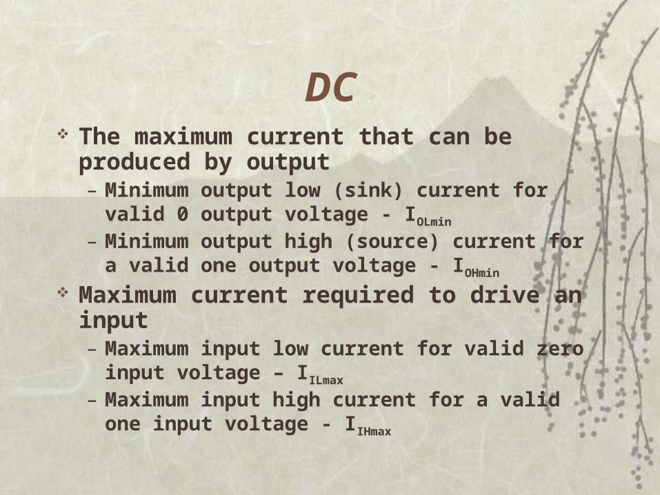
DC The maximum current that can be produced by
output– Minimum output low (sink) current for valid 0
output voltage - IOLmin
– Minimum output high (source) current for a valid one output voltage - IOHmin
Maximum current required to drive an input– Maximum input low current for valid zero input
voltage – IILmax
– Maximum input high current for a valid one input voltage - IIHmax
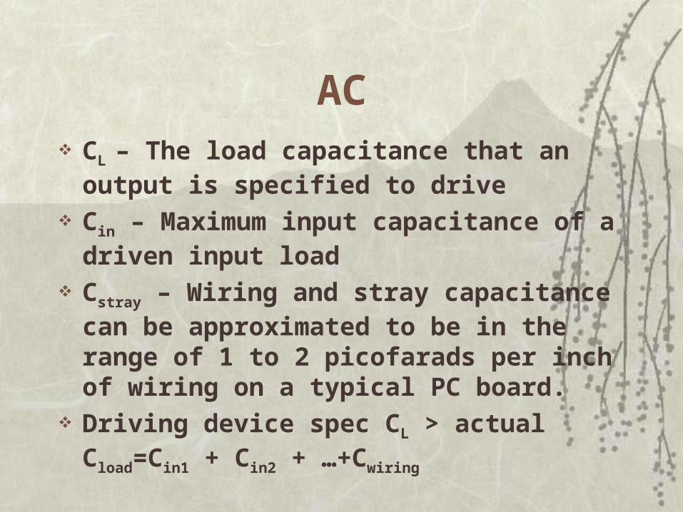
AC CL – The load capacitance that an output is
specified to drive Cin – Maximum input capacitance of a driven
input load Cstray – Wiring and stray capacitance can be
approximated to be in the range of 1 to 2 picofarads per inch of wiring on a typical PC board.
Driving device spec CL > actual Cload=Cin1 + Cin2 + …+Cwiring
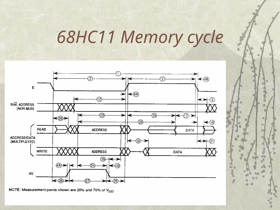
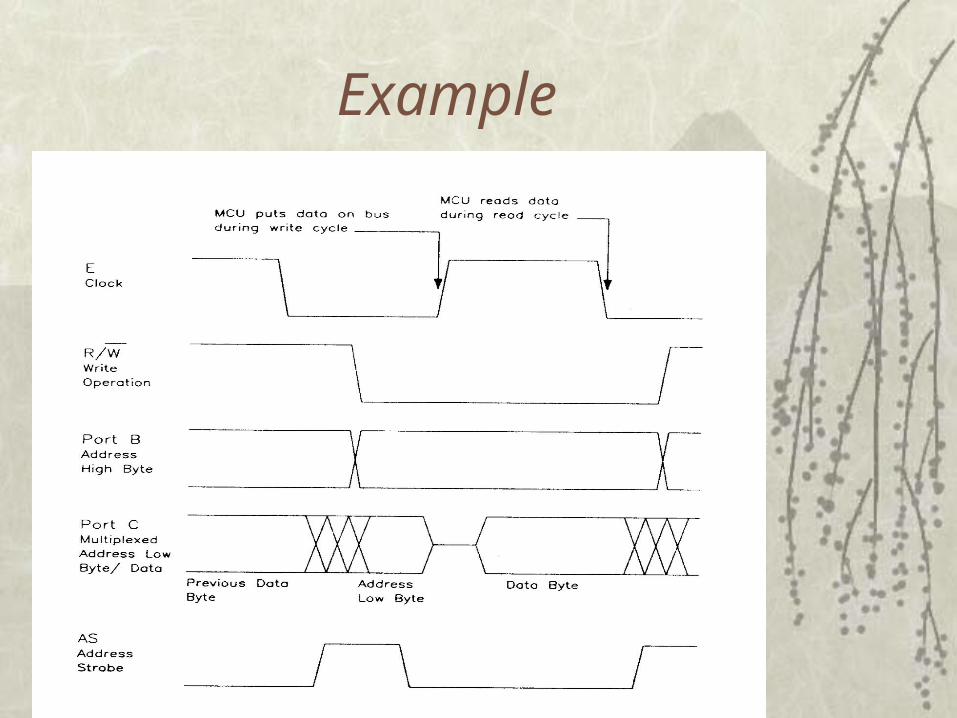
68HC11 Memory cycle
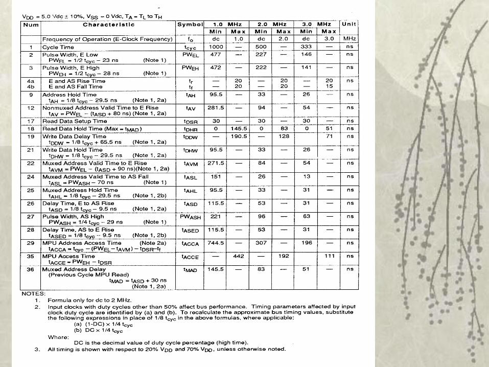
Note that in the HC11 Address information is provided to the external device (using the
multiplexed address/data bus) in the low half cycle of the E-clock Data to be read/written is placed on the data bus only in the high half
cycle of the E-clock All read and write operations MUST take place in 1 E-cycle
– External devices and circuitry must be designed to meet this requirement
– Cannot use “wait states” as you can in other microprocessor systems
• 8085: Slower devices can use READY input to request wait states
• Processor maintains address, data, and control signals
Expanded multiplexed mode
68HC11 supplies external bus signals– Port B = A15-A8– Port C = A7-A0 multiplexed with D7-D0
Address usually must be valid during entire operation– Need to latch A7-A0 (using 74HC373, for example)
Use external logic to derive control signals– Chip enable/select– Read/Write– Output enable
Error detection and correction
Errors– Soft error– Hard error
Confidence Checks– Parity– Hamming code– Checksum– CRC
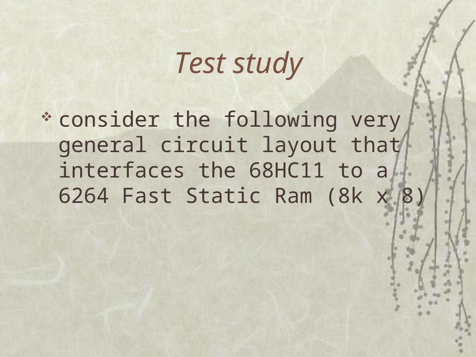
Test study
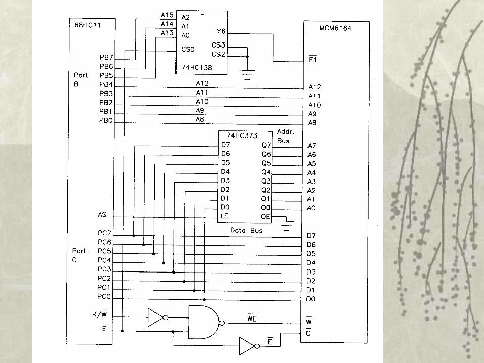
consider the following very general circuit layout that interfaces the 68HC11 to a 6264 Fast Static Ram (8k x 8)
Example
74373 is used as the address latch to “save” the lower 8 bits of the address that are on Port C only during the first half of the E-clock cycle
Discrete logic is used to derive the write and read enable signals for the memory chip (W* and G*)
– Both can only be asserted in the second half of the E-clock cycle 74138 is used for address decoding to generate a memory chip enable
(chip select) signal (E1*)
– Since the E-clock enables the 138, the decoder is only active in 2nd half cycle
– Memory chip can not be enabled in the 1st half cycle
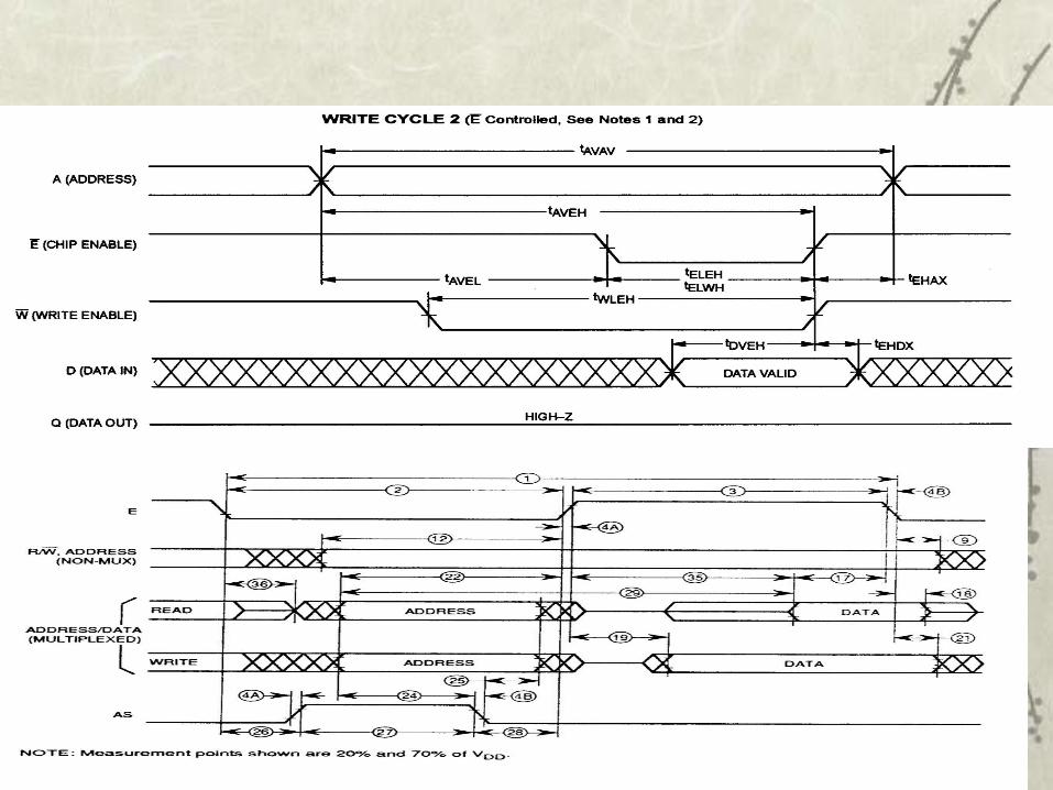
Timing relationship
Timing relationships are derived by comparing the timing diagrams of the memory chip and the HC11 and considering the external circuitry where necessary.
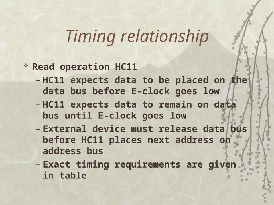
Read operation HC11
• E-clock goes low
• Address information placed on address bus, AS pulsed to trigger address latch
• E-clock goes high
• HC11 expects data to be placed on data bus
• E-clock goes low again and process repeats
Timing relationship
Read operation HC11 – HC11 expects data to be placed on the data
bus before E-clock goes low– HC11 expects data to remain on data bus
until E-clock goes low– External device must release data bus before
HC11 places next address on address bus– Exact timing requirements are given in table
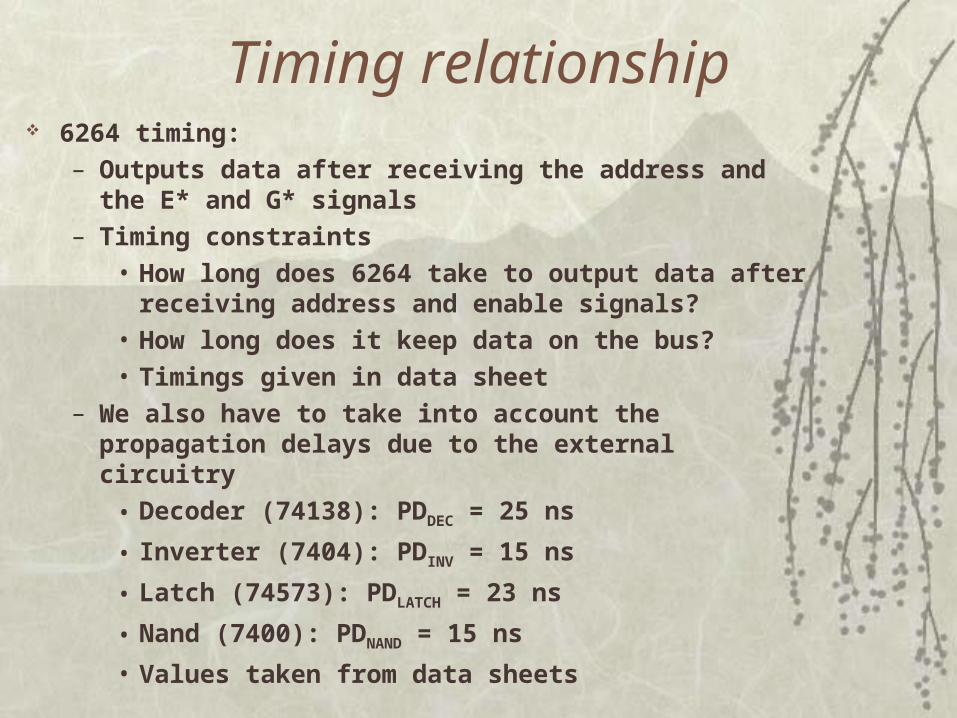
Timing relationship 6264 timing:
– Outputs data after receiving the address and the E* and G* signals
– Timing constraints
• How long does 6264 take to output data after receiving address and enable signals?
• How long does it keep data on the bus?
• Timings given in data sheet
– We also have to take into account the propagation delays due to the external circuitry
• Decoder (74138): PDDEC = 25 ns
• Inverter (7404): PDINV = 15 ns
• Latch (74573): PDLATCH = 23 ns
• Nand (7400): PDNAND = 15 ns
• Values taken from data sheets
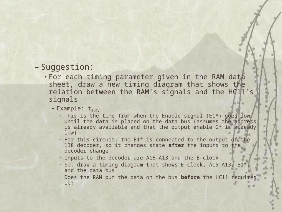
– Suggestion:• For each timing parameter given in the RAM data sheet,
draw a new timing diagram that shows the relation between the RAM’s signals and the HC11’s signals– Example: tELQV
• This is the time from when the Enable signal (E1*) goes low until the data is placed on the data bus (assumes the address is already available and that the output enable G* is already low)
• For this circuit, the E1* is connected to the output of the 138 decoder, so it changes state after the inputs to the decoder change
• Inputs to the decoder are A15-A13 and the E-clock• So, draw a timing diagram that shows E-clock, A15-A13, E1*, and
the data bus• Does the RAM put the data on the bus before the HC11 requires it?
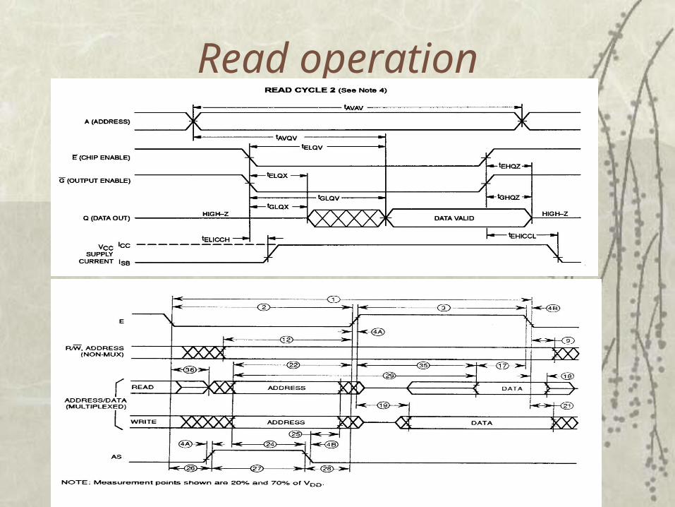
Read operation
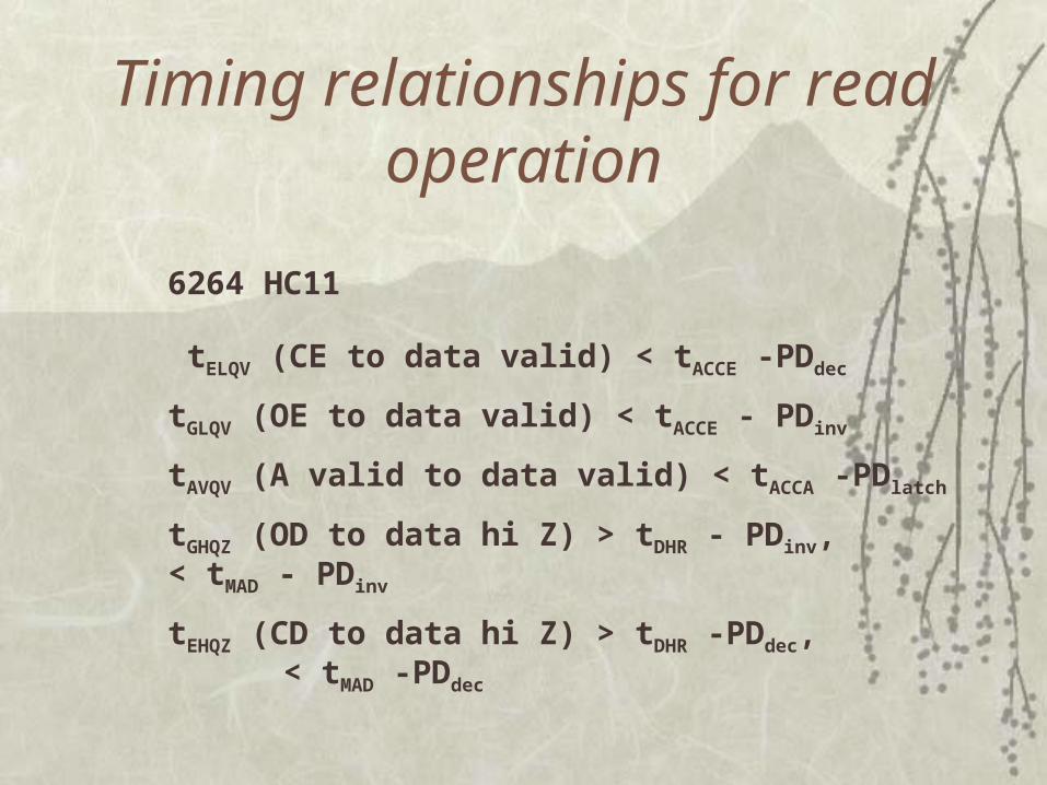
Timing relationships for read operation
6264 HC11
tELQV (CE to data valid) < tACCE -PDdec
tGLQV (OE to data valid) < tACCE - PDinv
tAVQV (A valid to data valid) < tACCA -PDlatch
tGHQZ (OD to data hi Z) > tDHR - PDinv, < tMAD - PDinv
tEHQZ (CD to data hi Z) > tDHR -PDdec, < tMAD -PDdec
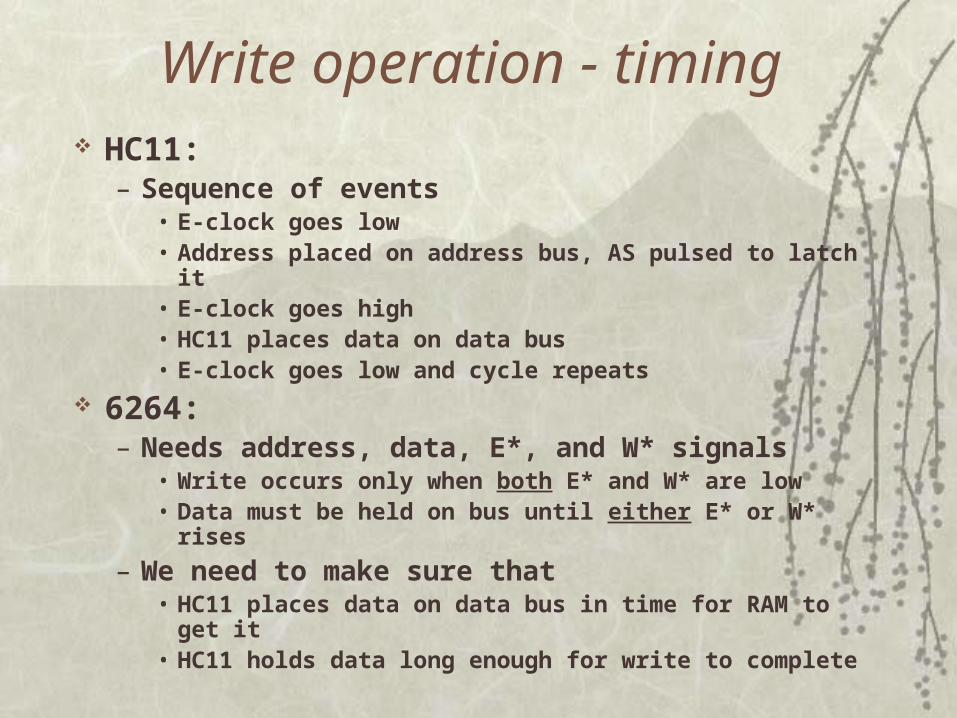
Write operation - timing HC11:
– Sequence of events• E-clock goes low• Address placed on address bus, AS pulsed to latch it• E-clock goes high• HC11 places data on data bus• E-clock goes low and cycle repeats
6264:– Needs address, data, E*, and W* signals
• Write occurs only when both E* and W* are low• Data must be held on bus until either E* or W* rises
– We need to make sure that • HC11 places data on data bus in time for RAM to get it • HC11 holds data long enough for write to complete
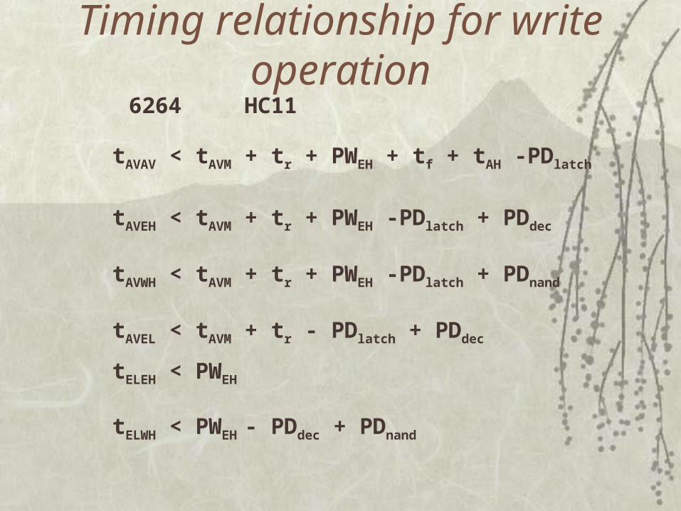
Timing relationship for write operation
6264 HC11
tAVAV < tAVM + tr + PWEH + tf + tAH -PDlatch
tAVEH < tAVM + tr + PWEH -PDlatch + PDdec
tAVWH < tAVM + tr + PWEH -PDlatch + PDnand
tAVEL < tAVM + tr - PDlatch + PDdec
tELEH < PWEH
tELWH < PWEH - PDdec + PDnand
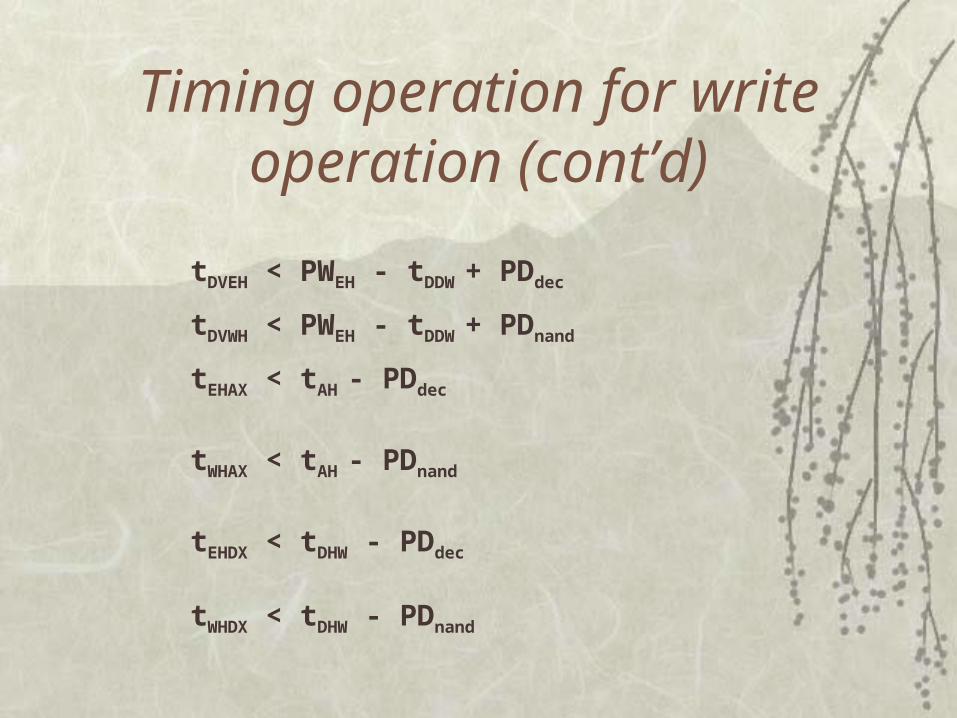
Timing operation for write operation (cont’d)
tDVEH < PWEH - tDDW + PDdec
tDVWH < PWEH - tDDW + PDnand
tEHAX < tAH - PDdec
tWHAX < tAH - PDnand
tEHDX < tDHW - PDdec
tWHDX < tDHW - PDnand
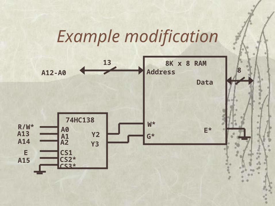
Example modification
Address
Data
E*W*
G*
8K x 8 RAM
74HC138
Y2Y3
A0A1A2
CS1CS2*CS3*
813
A12-A0
R/W*A13A14
EA15
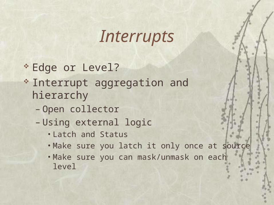
Interrupts
Edge or Level? Interrupt aggregation and hierarchy
– Open collector– Using external logic
• Latch and Status
• Make sure you latch it only once at source
• Make sure you can mask/unmask on each level
Assignment
Calculate what is the base address of 6164 in the circuit from Slide 22 and Example modification.