preliminary data sheet r2a20114afp/asp · preliminary data sheet r2a20114afp/asp continuous...
TRANSCRIPT
R03DS0051EJ0201 Rev.2.01 Page 1 of 16 Jan 08, 2016
Preliminary Data Sheet
R2A20114AFP/ASP Continuous Conduction Mode Interleaving PFC Control IC
Description
R2A20114AFP/ASP is a boost converter control IC with PFC (Power Factor Correction). Employing continuous conduction mode interleaving PFC, it performs higher efficiency and lower switching noise even for high power use. Interleaving control of the boost converters, namely, producing 180 degrees phase shift between the output signals (GD1,2) driving the boost converters, enables the system to perform high conversion efficiency and low switching noises and, at the same time, to reduces ripple currents in input and output current and then this allows use of smaller components such as boost inductors, input filters and output capacitors. R2A20114AFP/ASP integrates a various kinds of protection circuits, such as the detection circuit of breaking of wire in feedback loop, two modes of over voltage protection circuits, over current protection circuit and error output circuit (*1), which improve the reliability of the power supply system and reduce the number of component parts on the system.
Features
• Maximum Ratings ⎯ Supply voltage Vcc: 24 V ⎯ Junction temperature Tj: from –40 to +150 degrees centigrade
• Electrical characteristics ⎯ VFB feedback voltage VREF: 2.5 V ± 1.5% ⎯ UVLO (Undervoltage Lockout) operation start voltage VH: 10.4 V ± 0.7 V ⎯ UVLO operation shutdown voltage VL: 8.9 V ± 0.5 V ⎯ UVLO hysteresis voltage Hysuvl : 1.5 V ± 0.5 V
• Functions ⎯ Boost converter control with continuous conduction mode ⎯ Interleaving control ⎯ Frequency modulation (*2) ⎯ Brownout ⎯ Phase drop (*1) ⎯ External clock synchronization input ⎯ External clock synchronization output (*1) ⎯ Two modes of over voltage protections
Mode 1: Dynamic OVP preventing over voltage after sudden variation of load. Mode 2: Static OVP preventing over voltage in the period of normal operation.
⎯ Feedback loop wire breaking/open detector ⎯ Dual over voltage protection circuits (*1): FB and OVP2 terminals ⎯ Current balance control ⎯ Phase 1 and Phase 2 independent over current protection ⎯ Package line-up
Pb-free LQFP-40 (R2A20114AFP) Pb-free SOP-20 (R2A20114ASP)
Notes: *1 Supported only by R2A20114AFP *2 Frequency modulation periods (dfm) of R2A20114ASP are fixed.
R03DS0051EJ0201Rev.2.01
Jan 08, 2016
R2A20114AFP/ASP Preliminary
R03DS0051EJ0201 Rev.2.01 Page 2 of 16 Jan 08, 2016
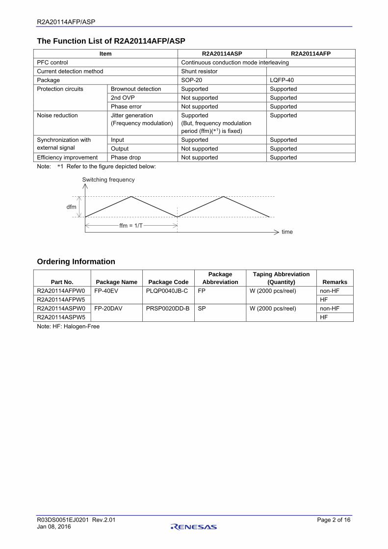
The Function List of R2A20114AFP/ASP
Item R2A20114ASP R2A20114AFP
PFC control Continuous conduction mode interleaving
Current detection method Shunt resistor
Package SOP-20 LQFP-40
Protection circuits Brownout detection Supported Supported
2nd OVP Not supported Supported
Phase error Not supported Supported
Noise reduction Jitter generation (Frequency modulation)
Supported (But, frequency modulation period (ffm)(*1) is fixed)
Supported
Synchronization with external signal
Input Supported Supported
Output Not supported Supported
Efficiency improvement Phase drop Not supported Supported
Note: *1 Refer to the figure depicted below:
Switching frequency
time
dfm
ffm = 1/T
Ordering Information
Part No. Package Name Package CodePackage
Abbreviation Taping Abbreviation
(Quantity) Remarks
R2A20114AFPW0 FP-40EV PLQP0040JB-C FP W (2000 pcs/reel) non-HF
R2A20114AFPW5 HF
R2A20114ASPW0 FP-20DAV PRSP0020DD-B SP W (2000 pcs/reel) non-HF
R2A20114ASPW5 HF
Note: HF: Halogen-Free

R2A20114AFP/ASP Preliminary
R03DS0051EJ0201 Rev.2.01 Page 3 of 16 Jan 08, 2016
Pin Arrangement of R2A20114AFP
N.C.
VCC
OV
P2
CS1
N.C.
CSO2
N.C
.
N.C
.
CSO1
E-DELAY
N.C.
VREF
AGND
FMR
BO
CS2
VAC
PD
SS
FB
N.C
.
CO
MP
RT
/SY
NC
GD
1
N.C
.
SY
NC
-O
N.C.
N.C
.
FMC
CT
PG
ND
N.C
.
N.C.
RS
GD
2
N.C
.
N.C.
IRAMP
ER
RO
R
OF
F
1
10
9
8
7
6
5
4
3
2
11
20
19
18
17
16
15
14
13
12
30
21
22
23
24
25
26
27
28
29
40
31
32
33
34
35
36
37
38
39
(Top view)
Pin Functions of R2A20114AFP
Pin No. Pin Name Function 1 FMR Frequency modulation setting resistor connecting terminal 2 FMC Frequency modulation setting capacitor connecting terminal 3 VREF Reference voltage output terminal 4 BO Brownout input terminal 5 VAC AC voltage input terminal 6 PD Phase drop input terminal 7 AGND Analog ground 8 E-DELAY Delay of the Error signal setting terminal
9, 10 N.C. Open 11 ERROR Error output terminal 12 OFF Shutdown terminal (VCC Reset) 13 RS Current correction setting resistor connecting terminal 14 SS Soft start setting capacitor connecting terminal 15 COMP Error amplifier output terminal (to be phase-compensated) 16 N.C. Open 17 FB Error amplifier input terminal (feedback voltage input terminal) 18 QVP2 OVP2 input terminal
19-21 N.C. Open 22 IRAMP Ramp waveform setting resistor connecting terminal 23 CSO2 Current sense amplifier 2 output terminal (to be phase-compensated) 24 CSO1 Current sense amplifier 1 output terminal (to be phase-compensated) 25 CS2 Current sense 2 input terminal 26 CS1 Current sense 1 input terminal 27 N.C. Open 28 VCC Supply voltage terminal
29-31 N.C. Open 32 GD2 Converter 2 Power MOSFET drive terminal 33 PGND Power ground 34 GD1 Converter 1 Power MOSFET drive terminal 35 N.C. Open 36 SYNC-O Synchronization signal output terminal 37 RT/SYNC Frequency setting resistor connecting terminal / Sync. Signal input terminal 38 CT Frequency setting capacitor connecting terminal
39, 40 N.C. Open

R2A20114AFP/ASP Preliminary
R03DS0051EJ0201 Rev.2.01 Page 4 of 16 Jan 08, 2016
Pin Arrangement of R2A20114ASP
(Top view)
1
2
3
4
5
6
7
8
9
10
20
19
18
17
16
15
14
13
12
11
CS2
CS1
GD1
SS
VCC
GD2
CSO2
CT PGND
FBCOMP
CSO1AGND
RS
VREF
RT/SYNC
IRAMP
VAC
FM
BO
Pin Functions of R2A20114ASP
Pin No. Pin Name Function
1 RT/SYNC Frequency setting timing resistor connecting terminal / Sync. signal input terminal
2 CT Frequency setting timing capacitor connecting terminal
3 FM Frequency modulation setting timing capacitor connecting terminal
4 VREF Reference voltage output terminal
5 BO Brownout input terminal
6 VAC AC voltage input terminal
7 AGND Analog ground
8 RS Current correction setting resistor connecting terminal
9 SS Soft start setting capacitor connecting terminal
10 COMP Error amplifier output terminal (to be phase-compensated)
11 FB Error amplifier input terminal (feedback voltage input terminal)
12 IRAMP Ramp waveform setting resistor connecting terminal
13 CSO2 Current sense amplifier 2 output terminal (to be phase-compensated)
14 CSO1 Current sense amplifier Output 1 output terminal (to be phase-compensated)
15 CS2 Current sense 2 input terminal
16 CS1 Current sense 1 input terminal
17 VCC Supply voltage terminal
18 GD2 Converter 2 Power MOSFET drive terminal
19 PGND Power ground
20 GD1 Converter 1 Power MOSFET drive terminal

R2A20114AFP/ASP Preliminary
R03DS0051EJ0201 Rev.2.01 Page 5 of 16 Jan 08, 2016
Block Diagram of R2A20114AFP
PROTECTION
BLOCK
INTERLEAVE
Logic 1
INTERLEAVE
Logic 2
CURRENT FORMING
BLOCK 1
CURRENT FORMING
BLOCK 2
VCC
CS2
SYNC-OFMC AGND
VCC
OCP1
OCP2
UVL VREF
OCP1
OCP2
2.5V
OSC1
OSC2
E-AMP
300nA
28μA
VREF
500nA
VREF
VREF
300nA
UVL
BO 4
RT/SYNC 37
CT 38
FMR 1
25
CS1 26
28
VREF3
GD134
IRAMP22
GD232
FB17
COMP15
SS14
0.82V/0.81V
0.31V
4V
VCC
OVP218
36
PD 6
ERROR 11
2.5V
PGND33
200nA
2
Latch(UVL Reset)
E-DELAY 8
OFF 12
VREF
CSO2 23
CSO1 24
OVP2
RS 13
VAC
7
UVL
100kΩ
OCP1
OCP2
10kΩ
UVL
GD1
GD2
0.31V
200nA
200nA
5.7V
OSC1
OSC2
OSC1
OSC2
CT
SYNC-O
SYNC-O
SOVP
FBOPEN
OVP2
DOVP
5
ERROR
BLOCK

R2A20114AFP/ASP Preliminary
R03DS0051EJ0201 Rev.2.01 Page 6 of 16 Jan 08, 2016
Block Diagram of R2A20114ASP
CURRENT FORMING
BLOCK 1
CURRENT FORMING
BLOCK 2
VCC
RT/SYNC
COMP
FM AGND
VCC
OCP1
OCP2
UVL VREF
OCP1
OCP2
2.5V
OSC1
OSC2
E-AMP
800nA
28μA
VREF
VREF
300nA
UVLCS2 15
BO
CS1 16
0.82V/0.81V
0.31V
4V
VCC
VREF
CSO1
FB
UVL
10kΩ
UVL
0.31V
200nA
200nA
5.7V
OSC1
OSC2
OSC1
OSC2
CT
SOVP
FBOPEN
DOVP
14
VAC 6
RS 8
CSO2 13
5
1
CT 2
3 7
SS9
10
FB11
PGND19
GD218
GD120
VREF4
17
IRAMP12
INTERLEAVE
Logic 2
INTERLEAVE
Logic 1
PROTECTION
BLOCK

R2A20114AFP/ASP Preliminary
R03DS0051EJ0201 Rev.2.01 Page 7 of 16 Jan 08, 2016
Absolute Maximum Ratings
Item Symbol Value Unit Note
Supply voltage VCC –0.3 to +24 V 3
GD1 and 2 Peak current Ipk-gd1, Ipk-gd2 ±1 A 3, 4
DC current Idc-gd1, Idc-gd2 ±0.1 A 3
Vref terminal current Iref –5 mA 3
Terminal current It-group ±1 mA 3, 5
RS terminal current Irs –500 μA 3
RT terminal current Irt –200 μA 3
IRAMP terminal current Iramp –200 μA 3
BO clamp current Ibo 300 μA 3
Terminal voltage Vt-group –0.3 to Vref V 3, 6
Vref terminal voltage Vt-ref –0.3 to Vref+0.3 V 3
SS terminal voltage Vt-ss –0.3 to Vref+1 V 3
Power dissipation Pt 1 W 3, 7
Operating ambient temperature Ta-opr –40 to +125 °C
Junction temperature Tj –40 to +150 °C 8
Storage temperature Tstg –55 to +150 °C
Notes: 1. Rated voltages are with reference to the AGND and PGND terminal.
2. For the direction of Rated currents, (+) denotes the current flowing into the IC, and (–) denotes the current flowing out of the IC.
3. Ambience temperature, Ta is 25 degrees centigrade.
4. Transient current when driving a capacitive load.
5. Rated currents of the terminals listed below: COMP, CSO1, CSO2
6. Rated voltages of the terminals listed below:
in the case of R2A20114AFP: CS1, CS2, VAC, RS, FB, PD, BO, ERROR, E-DLAY, OFF, OVP2, FMC, FMR, RT/SYNC, IRAMP, SYNC-O, CT, COMP, CSO1, CSO2
in the case of R2A20114ASP: CS1, CS2, VAC, RS, FB, BO, IRAMP, FM, RT/SYNC, CT, COMP, CSO1, CSO2
7. Thermal resistor
in the case of R2A20114AFP: θja = 85.3 degrees centigrade/W
in the case of R2A20114ASP: θja = 120 degrees centigrade/W
These values are obtained under the condition that the IC is mounted on the glass epoxy board, of which size is 50 × 50 × 1.6 [mm] and wiring density is 10%.
8. Stresses exceeding the absolute maximum ratings may damage the device. These are stress ratings only. Functional operation above the recommended operating ambient temperature range is not implied. Extended exposure to stresses above the absolute maximum ratings may affect device reliability.

R2A20114AFP/ASP Preliminary
R03DS0051EJ0201 Rev.2.01 Page 8 of 16 Jan 08, 2016
Electrical Characteristics
(Ta = 25°C, VCC = 12 V, CT = 1000 pF, RT = 27 kΩ, CS1, CS2 = GND, IRAMP = 10 kΩ, BO = 1 V, VAC = 0 V, RS = 220 kΩ, FMC = GND (*1), FM = GND (*2), FB = COMP)
Item Symbol Min Typ Max Unit Test Conditions
Supply UVLO turn-on threshold Vuvlh 9.7 10.4 11.1 V
UVLO turn-off threshold Vuvll 8.4 8.9 9.4 V
UVLO hysteresis Hysuvl 1.0 1.5 2.0 V
Standby current Istby — 100 160 μA VCC = 8.9 V
Operating current Icc — 5 7.5 mA
VREF Output voltage Vref 4.85 5.00 5.15 V Isource = –1 mA
Line regulation Vref-line — 5 20 mV Isource = –1 mA,
VCC = 10 V to 24 V
Load regulation Vref-load — 5 20 mV Isource = –1 mA to -5 mA
Temperature stability dVref — ±80 — ppm/°C Ta = –40 to 125°C (*3)
Error
amplifier
Feedback voltage Vfb 2.462 2.500 2.538 V FB-COMP Short
Input bias current (*1) Ifb –0.5 –0.3 –0.05 μA Measured pin: FB
Input bias current (*2) Ifb –1.3 –0.8 –0.25 μA Measured pin: FB
Open loop gain Av — 40 — dB (*3)
Upper clamp voltage Vclamp-comp 3.8 4.0 4.3 V FB = 2.0 V, COMP: Open
Low voltage Vl-comp 0.0 0.1 0.3 V FB = 3.0 V, COMP: Open
Source current Isrc-comp –190 –135 –80 μA FB = 1.5 V, COMP = 2.5 V
Sink current 1 Isnk-comp1 — 120 — μA (*3)
Sink current 2 Isnk-comp2 220 320 420 μA FB =3.5 V, COMP = 2.5 V
Transconductance gm 120 200 290 μs FB = 2.45 V ↔ 2.55 V,
COMP = 2.5 V
Brownout PFC enable voltage Von-pfc 0.74 0.82 0.9 V Input pin: BO
PFC disable voltage Voff-pfc 0.73 0.81 0.89 V Input pin: BO
Oscillator Initial accuracy fout 70 78 86 kHz Measured pin: OUT,
FMC = 0 V
fout temperature stability dfout/dTa — ±0.1 — %/°C Ta = –40 to 125°C (*3)
fout voltage stability fout-line –1.5 0.5 1.5 % VCC = 12 V to 18 V
CT top voltage Vct-H — 3.6 4.0 V (*3)
RT voltage Vrt 1.15 1.25 1.35 V
FMC sink current (*1)/
FM sink current (*2)
Isnk-fmc (*1)/
Isnk-fm (*2)
6 11 16 μA FMC = 1 V (*1)/
FM = 1 V (*2)
FMC source current (*1)/
FM source current (*2)
Iso-fmc (*1)/
Iso-fm (*2)
–16.5 –11.5 –6.5 μA FMC = 1 V (*1)/
FM = 1 V (*2)
FM magnitude change dfm 19 24 29 kHz FMC = 5 V (*1)/FM = 5 V (*2)
(*3, *4)
FM frequency 1 (*1) ffm1 0.25 0.38 0.5 kHz FMC = 6.8 nF, FMR = 4 V
(*4)
FM frequency 2 (*1) ffm2 14 25 35 kHz FMC = 220 pF, FMR = 1.2 V
(*4)
FM frequency (*2) ffm 6 10 14 kHz FM = 220 pF (*4)
Notes: *1 Applied to R2A20114AFP
*2 Applied to R2A20114ASP
*3 Design Specification (Reference data)
*4 Refer to the figure shown below:
Switching frequency
time
dfm
ffm = 1/T

R2A20114AFP/ASP Preliminary
R03DS0051EJ0201 Rev.2.01 Page 9 of 16 Jan 08, 2016
Electrical Characteristics (cont.)
(Ta = 25°C, VCC = 12 V, CT = 1000 pF, RT = 27 kΩ, CS1, CS2 = GND, IRAMP = 10 kΩ, BO = 1 V, VAC = 0 V, RS = 220 kΩ, FMC = GND (*1), FM = GND (*2), FB = COMP)
Item Symbol Min Typ Max Unit Test Conditions
Synchroni-
zation
SYNC threshold voltage
(rising)
Vsync 2.0 2.5 3.0 V
SYNC Min. pulse Psync 2 — — μs
SYNC-OUT shunt current
(*1)
Isync-s 5.0 — — mA
SYNC-OUT leakage current
(*1)
Isync-l — — 1.0 μA
Current
slope
RS output voltage 1 Vrs1 0.42 0.51 0.6 V VAC = 0 V, VOVP2 = 2.5 V
RS output voltage 2 Vrs2 –0.1 0 0.1 V VAC = 2.5 V, VOVP2 = 0 V
VAC bias current Ivac –0.8 –0.5 –0.2 μA Measured pin: VAC
Soft start Source current Iss –40 –28 –16 μA SS = 2 V
Phase drop Phase drop threshold
voltage (*1)
Vpd 2.4 2.5 2.6 V
Phase drop hysteresis (*1) Hya-pd 150 200 250 mV
PD bias current (*1) Ipd 0.05 0.2 0.5 μA Measured pin: PD
AMP1, 2 CSO offset voltage1 Voffset 0.68 0.88 1.0 V Vcs = 0 V
CSO offset voltage2 Vcaoh 2.83 3 3.17 V Vcs = 0.24 V
CS Bias current Ics-r –0.4 –0.2 –0.05 μA Measured pin: CS1, 2
Gate drive
1, 2
Gate drive rise time tr-gd — 30 100 ns CL = 500 pF
Gate drive fall time tf-gd — 30 100 ns CL = 500 pF
Gate drive low voltage Vol1-gd — 0.05 0.2 V Isink = 10 mA
Vol2-gd — 1 1.25 V Isink = 0.25 mA, VCC = 5 V
Gate drive high voltage Voh-gd 11.5 11.9 — V Isource = –10 mA
Minimum duty cycle Dmin-out — — 0 %
Maximum duty cycle Dmax-out 90 95 98 %
Over
voltage
protection
Dynamic OVP Threshold
voltage
Vdovp VFB×1.025
VFB×1.040
VFB×1.055
V
Static OVP Threshold
voltage
Vsovp VFB×1.065
VFB×1.080
VFB×1.095
V COMP = OPEN
Static OVP Hysteresis Hys-sovp 30 80 130 mV COMP = OPEN
OVP2 Threshold voltage (*1) Vovp2 VFB×1.065
VFB×1.080
VFB×1.095
μA
OVP2 Hysteresis (*1) Hys-ovp2 30 80 130 mV COMP = OPEN
OVP2 Bias current (*1) Iovp2 –0.8 –0.5 –0.2 μA Measured pin: OVP2
FB Open Detect Threshold
voltage
Vfbopen 0.45 0.5 0.55 V
FB Open Detect hysteresis Vfbopen 0.16 0.2 0.24 V
Over
current
protection
OCP Threshold voltage (*1) VCL 0.28 0.31 0.34 V
Delay to output td-CL — 100 250 ns
Notes: *1 Applied to R2A20114AFP
*2 Applied to R2A20114ASP

R2A20114AFP/ASP Preliminary
R03DS0051EJ0201 Rev.2.01 Page 10 of 16 Jan 08, 2016
Electrical Characteristics (cont.)
(Ta = 25°C, VCC = 12 V, CT = 1000 pF, RT = 27 kΩ, CS1, CS2 = GND, IRAMP = 10 kΩ, BO = 1 V, VAC = 0 V, RS = 220 kΩ, FMC = GND (*1), FM = GND (*2), FB = COMP)
Item Symbol Min Typ Max Unit Test Conditions
Error signal ERROR shunt current (*1) Ierror-s 5.0 — — mA
ERROR leakage current (*1) Ierror-l — — 1.0 μA
Phase error detect point Perror 1.1 1.35 1.6 — Vcso1 or 2 = 2.5 V,
Vcso2 or 1: sweep (*5)
OFF threshold voltage (*1) Voff 3.3 4.0 4.7 V
E-DELAY charge current (*1) Ied-c –55 –36 –20 μA
E-DELAY discharge current
(*1)
Ied-d 20 36 55 μA
E-DELAY threshold voltage
(*1)
Vdelay 2.35 2.45 2.55 V
Notes: *1 Applied to R2A20114AFP
*2 Applied to R2A20114ASP
*5 Refer to the figure shown below:
Perror =V'cso1(or 2)[V] – 0.55[V]
Vcso2(or 1)[V] – 0.55[V]
ERROR
CSO1(or 2) CSO2(or 1)
V'cso1(or 2)
Vcso2(or 1)

R2A20114AFP/ASP Preliminary
R03DS0051EJ0201 Rev.2.01 Page 11 of 16 Jan 08, 2016
Timing Chart
1. Vcc Start-up and Stop Timing
COMP
0.82V(Von-pfc)
10.4V (VH)
Soft Start
5V
4.0V
VCC
BO
FB
8.9V (VL)
VREF
VREF GOOD(Internal signal)
GD
SS
PFC-OFF(Internal signal)

R2A20114AFP/ASP Preliminary
R03DS0051EJ0201 Rev.2.01 Page 12 of 16 Jan 08, 2016
2. Stop Timing
SS
FB
GD
Normal operation
BO
0.81V(Voff-pfc)
PFC-OFF(Internal signal)
3. Overvoltage Protection (OVP)
VFB
GD OFF(Internal signal)
GD
Vsovp and Vovp2:VFB×1.08V
Isnk-comp2
Hys-sovp: 80mVVdovp: VFB×1.04V
COMP

R2A20114AFP/ASP Preliminary
R03DS0051EJ0201 Rev.2.01 Page 13 of 16 Jan 08, 2016
4. Phase Drop (Applied to R2A20114AFP)
GD1
PD 2.5V
GD2
5. ERROR (Applied to R2A20114AFP)
ERROR
Abnormal Operation(Phase Error, OVP2, E-Delay)
Normal Operation
Low Voltage (0V)
High Voltage

R2A20114AFP/ASP Preliminary
R03DS0051EJ0201 Rev.2.01 Page 14 of 16 Jan 08, 2016
System Diagram (Applied to R2A20114AFP)
L1 Vout
L2
To Dr1
To Dr2
Dr1
D1
D2
CoutCin
Rfb2
Rfb1
Ro2
Ro1
MCU
CS1
CS1
CS2
Vref
Vref
Vref
Dr2
CS2
+
PROTECTION
BLOCK
INTERLEAVE
Logic 1
INTERLEAVE
Logic 2
CURRENT FORMING
BLOCK 1
CURRENT FORMING
BLOCK 2
VCC
CS2
SYNC-OFMC AGND
VCC
OCP1
OCP2
UVL VREF
OCP1
OCP2
2.5V
OSC1
OSC2
E-AMP
300nA
28μA
VREF
VREF
300nA
UVL
BO4
RT/SYNC37
CT38
FMR1
25
CS126
28
VREF3
GD134
IRAMP22
GD232
FB17
COMP15
SS14
0.82V/0.81V
0.31V
4V
VCC
OVP218
36
PD6
ERROR11
2.5V
PGND33
200nA
2
Latch
(UVL Reset)
E-DELAY8
OFF 12
VREF
CSO223
CSO124
OVP2
RS13
VAC
7
UVL
100kΩ
OCP1
OCP2
10kΩ
UVL
GD1
GD2
0.31V
200nA
200nA
5.7V
OSC1
OSC2
OSC1
OSC2
CT
SYNC-O
SYNC-O
SOVP
FBOPEN
OVP2
DOVP
5
ERROR
BLOCK
500nA
VREF

R2A20114AFP/ASP Preliminary
R03DS0051EJ0201 Rev.2.01 Page 15 of 16 Jan 08, 2016
System Diagram (Applied to R2A20114ASP)
L1 Vout
L2
To Dr1
To Dr2
Dr1
D1
D2
CoutCin
Rfb2
Rfb1CS1
CS1
CS2
Dr2
CS2
+
FM AGND
CSO1
RS
VAC
CURRENT FORMING
BLOCK 1
CURRENT FORMING
BLOCK 2
VCC
RT/SYNC
COMP
VCC
OCP1
OCP2
UVL VREF
OCP1
OCP2
2.5V
OSC1
OSC2
E-AMP
800nA
28μA
VREF
VREF
300nA
UVL
CS215
BO
CS116
0.82V/0.81V
0.31V
4V
VCC
VREF
FB
UVL
10kΩ
UVL
0.31V
200nA
200nA
5.7V
OSC1
OSC2
OSC1
OSC2
CT
SOVP
FBOPEN
DOVP
14
6
8
CSO213
5
1
CT2
3 7
SS9
10
FB11
PGND19
GD218
GD120
VREF4
17
IRAMP12
INTERLEAVE
Logic 2
INTERLEAVE
Logic 1
PROTECTION
BLOCK

R2A20114AFP/ASP Preliminary
R03DS0051EJ0201 Rev.2.01 Page 16 of 16 Jan 08, 2016
Package Dimensions
• R2A20114AFP
NOTE)1. DIMENSIONS"*1"AND"*2"
DO NOT INCLUDE MOLD FLASH2. DIMENSION"*3"DOES NOT
INCLUDE TRIM OFFSET.
0.600.40
0.575
0.575
0.220.08
MaxNomMin
Dimension in MillimetersSymbol
Reference
7.0
0.13
0.10
0.13
8.8 9.0 9.2
0.50
7.0
9.29.08.8
0.270.220.17
0.200.150.10
0.65
8°0°
1.0
1.70
1.40
Previous CodeJEITA Package Code RENESAS Code
PLQP0040JB-C FP-40EV
MASS[Typ.]
0.2gP-LQFP40-7x7-0.65
e
HE
L
A1
D
E
A2
HD
A
bp
b1
c
xy
ZD
ZE
L1
c1
θDetail F
cA
L
Terminal cross section
(Ni/Pd/Au plating)
c
40
1
F
Mx
11
10
31
30 21
20
*3
*2
*1
Index mark
S
y S
D
E
e
HD
ZD
bp
HE
ZE
θ
bp
A1
A2
L1
• R2A20114ASP
NOTE)
1. DIMENSIONS"*1 (Nom)"AND"*2" DO NOT INCLUDE MOLD FLASH.
2. DIMENSION"*3"DOES NOT INCLUDE TRIM OFFSET.
12.60
1.15
0.12
0° 8°
7.80
0.15 0.20 0.25
0.46
0.00 0.10 0.20
5.50
0.50 0.70 0.90
2.20
ReferenceSymbol
Dimension in Millimeters
Min Nom Max
13.0
e
HE
L
A
D
E
A2
A1
bp
b1
c
xy
Z
L1
c1
θ
0.34 0.40
8.007.50
1.27
0.15
0.80
Previous CodeJEITA Package Code RENESAS Code
PRSP0020DD-B FP-20DAV
MASS[Typ.]
0.31gP-SOP20-5.5x12.6-1.27
Terminal cross section
(Ni/Pd/Au plating)
c
Detail F
L
y
S
S
Index mark
1
x M
*3
*2
*1
F
10
1120
A
Z e
E
D
θ
L1
A1
bp
bp
HE

Notice1. Descriptions of circuits, software and other related information in this document are provided only to illustrate the operation of semiconductor products and application examples. You are fully responsible for
the incorporation of these circuits, software, and information in the design of your equipment. Renesas Electronics assumes no responsibility for any losses incurred by you or third parties arising from the
use of these circuits, software, or information.
2. Renesas Electronics has used reasonable care in preparing the information included in this document, but Renesas Electronics does not warrant that such information is error free. Renesas Electronics
assumes no liability whatsoever for any damages incurred by you resulting from errors in or omissions from the information included herein.
3. Renesas Electronics does not assume any liability for infringement of patents, copyrights, or other intellectual property rights of third parties by or arising from the use of Renesas Electronics products or
technical information described in this document. No license, express, implied or otherwise, is granted hereby under any patents, copyrights or other intellectual property rights of Renesas Electronics or
others.
4. You should not alter, modify, copy, or otherwise misappropriate any Renesas Electronics product, whether in whole or in part. Renesas Electronics assumes no responsibility for any losses incurred by you or
third parties arising from such alteration, modification, copy or otherwise misappropriation of Renesas Electronics product.
5. Renesas Electronics products are classified according to the following two quality grades: "Standard" and "High Quality". The recommended applications for each Renesas Electronics product depends on
the product's quality grade, as indicated below.
"Standard": Computers; office equipment; communications equipment; test and measurement equipment; audio and visual equipment; home electronic appliances; machine tools; personal electronic
equipment; and industrial robots etc.
"High Quality": Transportation equipment (automobiles, trains, ships, etc.); traffic control systems; anti-disaster systems; anti-crime systems; and safety equipment etc.
Renesas Electronics products are neither intended nor authorized for use in products or systems that may pose a direct threat to human life or bodily injury (artificial life support devices or systems, surgical
implantations etc.), or may cause serious property damages (nuclear reactor control systems, military equipment etc.). You must check the quality grade of each Renesas Electronics product before using it
in a particular application. You may not use any Renesas Electronics product for any application for which it is not intended. Renesas Electronics shall not be in any way liable for any damages or losses
incurred by you or third parties arising from the use of any Renesas Electronics product for which the product is not intended by Renesas Electronics.
6. You should use the Renesas Electronics products described in this document within the range specified by Renesas Electronics, especially with respect to the maximum rating, operating supply voltage
range, movement power voltage range, heat radiation characteristics, installation and other product characteristics. Renesas Electronics shall have no liability for malfunctions or damages arising out of the
use of Renesas Electronics products beyond such specified ranges.
7. Although Renesas Electronics endeavors to improve the quality and reliability of its products, semiconductor products have specific characteristics such as the occurrence of failure at a certain rate and
malfunctions under certain use conditions. Further, Renesas Electronics products are not subject to radiation resistance design. Please be sure to implement safety measures to guard them against the
possibility of physical injury, and injury or damage caused by fire in the event of the failure of a Renesas Electronics product, such as safety design for hardware and software including but not limited to
redundancy, fire control and malfunction prevention, appropriate treatment for aging degradation or any other appropriate measures. Because the evaluation of microcomputer software alone is very difficult,
please evaluate the safety of the final products or systems manufactured by you.
8. Please contact a Renesas Electronics sales office for details as to environmental matters such as the environmental compatibility of each Renesas Electronics product. Please use Renesas Electronics
products in compliance with all applicable laws and regulations that regulate the inclusion or use of controlled substances, including without limitation, the EU RoHS Directive. Renesas Electronics assumes
no liability for damages or losses occurring as a result of your noncompliance with applicable laws and regulations.
9. Renesas Electronics products and technology may not be used for or incorporated into any products or systems whose manufacture, use, or sale is prohibited under any applicable domestic or foreign laws or
regulations. You should not use Renesas Electronics products or technology described in this document for any purpose relating to military applications or use by the military, including but not limited to the
development of weapons of mass destruction. When exporting the Renesas Electronics products or technology described in this document, you should comply with the applicable export control laws and
regulations and follow the procedures required by such laws and regulations.
10. It is the responsibility of the buyer or distributor of Renesas Electronics products, who distributes, disposes of, or otherwise places the product with a third party, to notify such third party in advance of the
contents and conditions set forth in this document, Renesas Electronics assumes no responsibility for any losses incurred by you or third parties as a result of unauthorized use of Renesas Electronics
products.
11. This document may not be reproduced or duplicated in any form, in whole or in part, without prior written consent of Renesas Electronics.
12. Please contact a Renesas Electronics sales office if you have any questions regarding the information contained in this document or Renesas Electronics products, or if you have any other inquiries.
(Note 1) "Renesas Electronics" as used in this document means Renesas Electronics Corporation and also includes its majority-owned subsidiaries.
(Note 2) "Renesas Electronics product(s)" means any product developed or manufactured by or for Renesas Electronics.
http://www.renesas.comRefer to "http://www.renesas.com/" for the latest and detailed information.
Renesas Electronics America Inc.2801 Scott Boulevard Santa Clara, CA 95050-2549, U.S.A.Tel: +1-408-588-6000, Fax: +1-408-588-6130Renesas Electronics Canada Limited9251 Yonge Street, Suite 8309 Richmond Hill, Ontario Canada L4C 9T3Tel: +1-905-237-2004Renesas Electronics Europe LimitedDukes Meadow, Millboard Road, Bourne End, Buckinghamshire, SL8 5FH, U.KTel: +44-1628-585-100, Fax: +44-1628-585-900Renesas Electronics Europe GmbHArcadiastrasse 10, 40472 Düsseldorf, Germany Tel: +49-211-6503-0, Fax: +49-211-6503-1327Renesas Electronics (China) Co., Ltd.Room 1709, Quantum Plaza, No.27 ZhiChunLu Haidian District, Beijing 100191, P.R.ChinaTel: +86-10-8235-1155, Fax: +86-10-8235-7679Renesas Electronics (Shanghai) Co., Ltd.Unit 301, Tower A, Central Towers, 555 Langao Road, Putuo District, Shanghai, P. R. China 200333 Tel: +86-21-2226-0888, Fax: +86-21-2226-0999Renesas Electronics Hong Kong LimitedUnit 1601-1611, 16/F., Tower 2, Grand Century Place, 193 Prince Edward Road West, Mongkok, Kowloon, Hong KongTel: +852-2265-6688, Fax: +852 2886-9022Renesas Electronics Taiwan Co., Ltd.13F, No. 363, Fu Shing North Road, Taipei 10543, TaiwanTel: +886-2-8175-9600, Fax: +886 2-8175-9670Renesas Electronics Singapore Pte. Ltd.80 Bendemeer Road, Unit #06-02 Hyflux Innovation Centre, Singapore 339949Tel: +65-6213-0200, Fax: +65-6213-0300Renesas Electronics Malaysia Sdn.Bhd.Unit 1207, Block B, Menara Amcorp, Amcorp Trade Centre, No. 18, Jln Persiaran Barat, 46050 Petaling Jaya, Selangor Darul Ehsan, MalaysiaTel: +60-3-7955-9390, Fax: +60-3-7955-9510Renesas Electronics India Pvt. Ltd.No.777C, 100 Feet Road, HAL II Stage, Indiranagar, Bangalore, IndiaTel: +91-80-67208700, Fax: +91-80-67208777Renesas Electronics Korea Co., Ltd.12F., 234 Teheran-ro, Gangnam-Gu, Seoul, 135-080, KoreaTel: +82-2-558-3737, Fax: +82-2-558-5141
SALES OFFICES
© 2016 Renesas Electronics Corporation. All rights reserved.Colophon 5.0