precise in situ tuning of the critical current of a
TRANSCRIPT

Precise in situ tuning of the critical current of a superconducting nanowire using high bias
voltage pulses
This article has been downloaded from IOPscience. Please scroll down to see the full text article.
2011 Nanotechnology 22 395302
(http://iopscience.iop.org/0957-4484/22/39/395302)
Download details:
IP Address: 130.126.13.245
The article was downloaded on 12/09/2011 at 07:00
Please note that terms and conditions apply.
View the table of contents for this issue, or go to the journal homepage for more
Home Search Collections Journals About Contact us My IOPscience

IOP PUBLISHING NANOTECHNOLOGY
Nanotechnology 22 (2011) 395302 (7pp) doi:10.1088/0957-4484/22/39/395302
Precise in situ tuning of the critical currentof a superconducting nanowire using highbias voltage pulsesThomas Aref and Alexey Bezryadin
University of Illinois at Urbana-Champaign, 1110 West Green Street Urbana, IL 61801, USA
E-mail: [email protected]
Received 13 May 2011, in final form 4 August 2011Published 5 September 2011Online at stacks.iop.org/Nano/22/395302
AbstractWe present a method for in situ tuning of the critical current (or switching current) and criticaltemperature of a superconducting MoGe nanowire using high bias voltage pulses. Our mainfinding is that as the pulse voltage is increased, the nanowire demonstrates a reduction, aminimum and then an enhancement of the switching current and critical temperature. Usingcontrolled pulsing, the switching current of a superconducting nanowire can be set exactly to adesired value. These results correlate with in situ transmission electron microscope imagingwhere an initially amorphous nanowire transforms into a single crystal nanowire by high biasvoltage pulses. We compare our transport measurements to a thermally activated model ofLittle’s phase slips in nanowires.
(Some figures in this article are in colour only in the electronic version)
Superconducting nanowires have unique superconductingproperties due to their one-dimensional nature. They havebeen proposed as candidates for device applications such asvarious solid state qubit implementations [1–3] and as photoncounters [4]. We describe a post-fabrication technique usinghigh bias voltage pulses that allows precise in situ control overthe critical current of a superconducting nanowire and explaina counterintuitive enhancement of the critical current observedwith higher pulse voltages.
We have performed experiments applying controlled highbias pulses to superconducting MoGe nanowires in situ. Weobserved a decrease of switching current, ISW, which ismeasured at a fixed temperature, typically 0.3 K. Analysisof the rate of Little’s phase slips indicates that pulsing alsocauses a decrease in the critical temperature, TC, of the wire.Initially, the wire maintains an overall behavior consistentwith being a homogeneous nanowire with a reduced switchingcurrent and critical temperature but no significant changein the normal resistance. As larger and larger pulses areapplied, the switching current reaches a minimum and thenstarts to increase, returning to values similar to or exceedingthe starting switching current. Critical temperature alsoreturns and normal resistance is observed to drop. Usingscanning electron microscope (SEM) and transmission electron
microscope (TEM) analysis, we find that this is a permanentmorphological change of the nanowire and not weak linkformation.
An interesting application of this effect is to control theswitching current of a superconducting nanowire, openingthe possibility of in situ engineered nanowires with preciseswitching currents (and to a lesser extent critical temperatures).We demonstrate that the switching current can be set to withinapproximately 10 nA of a desired value (see figure 1). Theswitching current cannot be more accurately defined as itsnatural stochastic behavior results in a distribution with astandard deviation of the order of 10 nA [5].
The nanowires were fabricated using the method ofmolecular templating [6]. Briefly, fluorinated single wallcarbon nanotubes (SWNTs) were suspended across a trenchin a Si substrate coated with SiO2 and SiN films. Mo76Ge24
is deposited by DC sputtering forming a nanowire by usingthe nanotube as a nanoscaffold. Pattern definition byphotolithography and the undercut of the trench allow onlyone conductance path, the nanowire, to be formed. Thesuperconducting properties of the nanowires were measuredin a He-4 (base temperature 1.5 K) or He-3 system (basetemperature 0.3 K). The nanowires were measured in astandard current biased setup with a low noise voltage source
0957-4484/11/395302+07$33.00 © 2011 IOP Publishing Ltd Printed in the UK & the USA1

Nanotechnology 22 (2011) 395302 T Aref and A Bezryadin
Figure 1. (a) ISW can be set exactly using a combination of large andsmall pulses. The flat regions correspond to the set value of ISW
where no pulsing is applied. The noisy regions correspond to ISW
being set to the desired value as pulsing is applied. In this example,the starting ISW was 1.07 μA and the chosen target values are shownby the green dotted lines. The pulse number represents the orderingof pulses in time and is not proportional to the pulse amplitude.Some pulses have zero amplitude, namely those corresponding to theplateaus of ISW. (b) Close-up of the effect of pulsing on ISW as VP isincreased from 0 to 0.326 V. As VP grows, ISW becomes increasinglystochastic until at large enough pulses we observe a strong downwardtrend. In this case, the drop in ISW occurs at pulse number 73 forVP = 0.326 V. (c) Setting of ISW to 0.85 μA with accompanyingvoltage pulses. At first large pulses are applied to get ISW near thedesired value. Then smaller pulses are applied to bounce the ISW tothe exact value desired.
feeding a large value standard resistor Rstd serving as a currentsource and separate voltage probes.
The four-probe measurement is of the superconductingelectrodes in series with the nanowire, not just the nanowireitself. The electrodes go superconducting at a temperatureconsiderably higher than the nanowire does and they are alsoseamlessly connected to the nanowire so the contact resistanceis zero. Thus the performed measurements give the resistanceof the wire only. We name this type of arrangement of thecurrent and voltage probes a quasi-four-probe measurement.In order to protect sensitive measurement equipment from highbias pulses (1 V or more) and to allow application of a voltagebias rather than a current bias pulse, a switching system wasemployed to switch between measurement mode and pulsingmode (see figure 2(a)). In order to study the effect of voltagepulsing, the wire was pulsed between sensitive measurementsbut not during the measurements.
Both manually operated switches and automated relays(voltage powered switches controlled by a computer) wereused. No difference in behavior of the nanowires wasobserved between the two. The relays were low bias, latchingrelays powered by a Keithley electrometer controlled by the
Figure 2. Experimental setup: (a) four relays (voltage controlledswitches) are used to switch between measurement and pulsingmode. In measurement mode (all relays in position 1), we canmeasure either voltage versus current curves (amplitude of current≈1–10 μA) or resistance versus temperature curves (amplitude ofcurrent ≈10–20 nA). A sine wave generator connected throughRstd = 0.1–1 M� forms a current source connected to the left lead.A small voltage (≈1–10 mV) is measured on the two center leads.The right current lead is grounded. In pulsing mode (relays inposition 2), a single high bias voltage pulse (≈0.1–1 V) is sent in onthe left current lead, the two center leads are disconnected and thepulse can be detected on the right lead using an ammeter(≈0.1–1 mA). (b) Example measured current going throughnanowire from a high bias voltage pulse measured with the ammeter.The pulse is 100 μs long and there are minor amounts of rounding ofthe pulse due to filtering in the cryostat.
measurement computer through a general purpose interfacebus. The latching design of the relays allows the powerto the relays to be removed without affecting the switchposition of the relays. To test the relays, repeated switcheswere made with no pulse application. No effect on anynanowire was observed from just switching back and forthwithout pulse application. Square pulses were applied usinga data acquisition (DAQ) card. Pulse duration was kept at100 μs and pulse voltage amplitude was varied. Pulses ofthis length transmit fairly well through the filtering system onthe cryogenic measurement systems, maintaining their squareshape with minimal rounding (see figure 2(b)). We have notsystematically explored the effect of different length pulses(or different shaped pulses) but we do not expect significantdependence on these two factors for the following reasons.The response time of the nanowire should be of the orderof picoseconds (the capacitance of the electrodes is of theorder of a few fF [7] while the resistance is approximately1 k� giving a RC time constant of approximately 1–10 ps)so the wire will have reached equilibrium current early in thepulse. The wire is expected to reach its maximum temperature(due to Joule heating) during the pulse and cool back to basetemperature after the pulse within 10–100 ns [5] so it should bewell thermally equilibrated early in the pulse as well. It shouldbe noted that our relay switching speed (it takes approximately1 s for the relay to switch between modes) is not fast enough toallow us to capture the cooldown back to base temperature after
2

Nanotechnology 22 (2011) 395302 T Aref and A Bezryadin
the pulse and the wire is well thermalized before switchingcurrents are measured after a pulse.
In measurement mode, a low bias sine wave signal currentsource is applied to the nanowire and the voltage is measuredseparately using the quasi-four-probe measurement describedpreviously (see figure 2(a)). Typical voltage versus current(VI) curves and the effects of pulsing on them are shownin figure 3. ISW initially decreases with minimal changein RN and IR and the VI curves maintain single hystereticloops characteristic of homogeneous wires. The hysteresisin the VI curve disappears as the switching current goesto a minimum (see figure 3(d)). A flat, superconductingregion indicates that a non-zero critical current always remains.Higher pulsing results in a return of the hysteretic VI curve withnow increasing ISW and decreasing RN as the pulse voltageis increased. When ISW returns, we generally observe phaseslip centers in the VI curves (see figure 3(e)) indicating lesshomogeneous nanowires. As pulse voltage is further increased,these phase slip centers gradually disappear. The wire canreturn to a ISW approaching the starting ISW (see figure 3(b))or even exceeding it (see figure 3(f)). From these types ofVI curves, we can extract the switching current, ISW, usingthreshold detection and the normal resistance, RN, using linearfitting and plot the data versus pulse number or pulse voltage,VP, across the nanowire. The effect as VP is increased from0 to 0.326 V in 5 mV steps is shown in figure 1(b). Forthe lowest voltage pulses, we primarily observe scatter fromthe natural stochasticity of the switching current [5]. In orderto minimize this natural stochasticity, we averaged over 100switching current measurements between pulses. As VP isincreased, we observe an increasing stochasticity of ISW whichquickly becomes greater than the natural stochasticity of theswitching current. As the pulse voltage increases further, wesee the irreversible drop of the switching current observed inthe VI curves. It should be noted that ISW was always measuredsufficiently long after the voltage pulse was finished that thewire had time to completely equilibrate to the bath temperature.Thus the observed changes in ISW are due to the voltage pulsepermanently altering the wire and not the heating effects of thehigh bias pulse. We can use this combined downward trendand increased stochasticity to precisely set ISW to a desiredvalue. As shown in figure 1(a), ISW is set to 10 values chosenuniformly from 0.95 to 0.05 μA. An example of a pulsesequence used to do this is shown in figure 1(c). Large pulsesare used to approach the desired value and then smaller pulses(with their enhanced stochasticity) are used to ‘bounce’ theswitching current to within ≈10 nA of the desired value. Foreach of the 10 chosen target values, the switching current wasset to the desired value.
The decrease and return of ISW seen in the VI curves canbe plotted versus VP in a similar fashion. It should be notedthat as the switching current goes through its minimum it ispoorly detected by this threshold detection scheme. The drop,saturation and return of ISW can be seen in figure 4. Theinitial drop of ISW does not have a corresponding change inRN. When ISW reaches a minimum and begins to return, RN
begins to drop. This behavior was consistent for all nanowiresmeasured and was reproduced on many nanowires (of whichfigure 4 contains four examples).
Figure 3. Voltage versus current (VI) curves demonstrating the effectof high bias pulses. (a) Initial application of high bias pulsesdecreases the switching current from ISW1 to ISW2 while minimallychanging RN and IR. (b) Further pulsing results in the return of ISW
and a drop in RN. ‘Initial’ is the same curve as the one shown inblack in graph (a). ‘Final’ is the last VI curve before the samplebroke. (c) A different nanowire with a smaller initial ISW. This graphshows many VI curves to indicate the gradual decrease of ISW asincreasing pulses are applied. (d) Application of higher pulses resultsin a loss of hysteresis of the VI curve. However, the VI curve retainsa flat, superconducting region with apparently non-zero criticalcurrent. (e) Still higher pulses results in the return of ISW with a dropin RN and evidence of phase slip centers. (f) Still higher pulsingproduces an almost uniform VI curve with ISW exceeding the originalswitching current and a further drop in RN. ‘Initial’ is the same curveas the one shown in black in (c). ‘Final’ is the last VI curve beforethe sample broke.
The resistance versus temperature curves taken after aseries of pulsing (see figures 5(a) and (b)) show behaviorconsistent with the observed ISW and RN behavior (for the RTcurve, the low bias current signal was reduced from ≈1–10 μAto 10–20 nA to measure the RT curve in the linear regime).The RT curves generally demonstrate one transition indicativeof a homogeneous wire with fitting parameters similar tounpulsed nanowires. The critical temperature, TC, of thenanowire decreases as pulse voltage increases saturating at aminimum. TC is defined as a fitting parameter in the best Littlefit (discussed in detail below). Further increase of pulse voltageresults in the increase of TC and the drop in RN (see figures 5(c)and (d)).
3

Nanotechnology 22 (2011) 395302 T Aref and A Bezryadin
Figure 4. Switching current, ISW, and normal resistance, RN, versusthe maximum pulse voltage, VP, applied to the wire. The blue line isISW which decreases and then increases with increasing pulseamplitude. The red line is RN, which stays constant and thendecreases. This is a counterintuitive result that was consistent on allnanowires measured and has been reproduced on several nanowiresof which (a), (b), (c) and (d) are four examples. The dashed lineindicates where both RN and ISW begin to rapidly decrease. Applyingpulses smaller than the maximum previous applied pulse does notlead to a significant change in ISW. (a) A nanowire with startingISW = 12.2 μA. The dashed line is at 1.105 V. ISW returns to11.0 μA before the wire abruptly breaks. (b) A wire with similarfabrication parameters to the one shown in (a) (the axes are the samefor graphs (a) and (b)). The starting ISW = 8.5 μA. The dashed lineis at 1.150 V. ISW returns to a maximum of 10.9 μA (which is greaterthan the starting ISW) before decreasing again until the wire breaks.(c) A third example nanowire with starting ISW = 10.3 μA andending ISW = 8.5 μA. The dashed line is at 0.502 V. Images of thiswire before and after pulsing are shown in figure 6. (d) A nanowirefabricated on a multi-walled carbon nanotube instead of a fluorinatedSWNT with starting ISW = 26.5 μA and ending ISW = 11.4 μA.The dotted line is at 0.947 V.
SEM imaging (figures 6(a) and (b)) before and afterpulsing show virtually no change in the nanowire, ruling outthe formation of obvious weak links. To more thoroughlystudy the effect of pulses on the nanowires, we turn to insitu TEM experiments. TEM experiments require differentsamples from those described previously. Most importantly,the nanowire must be across an open slit for TEM observation.We deposit multi-walled carbon nanotubes (MWNTs) acrossTEM compatible slits to generate these samples [8]. MWNTswere used for the TEM samples (instead of the SWNTs usedfor non-TEM compatible samples described above) becauseMWNTs are more robust and rigid and can thus more easilybe deposited on the TEM compatible slits (the SWNTs tendto sag into the TEM slits and not produce suitable nanowires).The MWNT scaffold makes for a less ideal wire than a SWNTsince the diameter of the MWNT (approximately 20 nm) iscomparable to the thickness of the metal film deposited to formthe nanowire while the diameter of the SWNT is much smaller(approximately 2 nm). The MWNTs may also contribute someshunt conductance so SWNTs were preferred when feasible.The SWNTs are fluorinated to make them fully insulating so
Figure 5. Resistance versus temperature curves and fits. (a) Four RTcurves taken as pulsing generally drives ISW down. From right to left,the corresponding pulse voltages are 0, 0.456, 0.600 and 0.614 V.The red curves are best fits to a thermally activated phase slip model.(b) Three RT curves taken when ISW returns for the same wire asshown in (a). From left to right the pulse voltages are 0.645, 0.679and 0.745 V. (c) ISW and TC versus VP for the wire whose RT curvesare shown in (a) and (b). The diamonds correspond to ISW and thestars correspond to TC. The dotted line is at 0.645 V where theturnaround from decreasing to increasing behavior occurs. (d) RN
and ξ(0) versus VP. The diamonds correspond to RN and the starscorrespond to ξ(0). Initially RN is flat while ξ(0) shows a growingtrend. After VP reaches 0.645 V, RN begins to drop and ξ(0) shows amaximum and saturates to a value higher than the starting value.
they do not contribute a shunt conductance to the resistancemeasurement (i.e. the measurement is completely dominatedby the superconducting wire). The change in scaffold does notaffect the pulsing behavior (see figure 4(d)).
The TEM compatible slits are formed using a KOH etch tofabricate a V-shaped cut in a silicon chip coated on both sideswith 100 nm of silicon nitride. The V-shaped cut almost piercesthe chip except for approximately 5 μm of remaining silicon.This silicon is cracked by sonicating in deionized water forless than a second. A 30–60 s KOH etch removes the crackedsilicon leaving an approximately 100 nm wide silicon nitridemembrane. This membrane is removed by reactive ion etching(RIE) from the etch pit side. The membrane is supportedduring the RIE step by a piece of polydimethylsiloxane(PDMS). In the method previously described [8] we removedthe silicon nitride entirely and oxidized the silicon to forman insulating layer. By etching the silicon nitride from theetch pit side, we are able to use the silicon nitride as theinsulating layer, thus skipping the oxidizing step. With thesesamples, we were able to perform in situ TEM experimentsto directly determine the effects of high bias voltage pulseson metal coated nanotubes. The in situ TEM experimentsmust be done at room temperature while superconductingmeasurements must be done at cryogenic temperatures. Wedo not expect this change in base temperature to produce asignificant difference as both experiments are performed undervacuum and the nanowire itself is expected to reach a hightemperature (≈2000 K) under a high bias voltage (≈0.5 V).
4

Nanotechnology 22 (2011) 395302 T Aref and A Bezryadin
Figure 6. SEM and TEM analysis: (a) SEM image of a nanowirebefore pulsing at cryogenic temperatures and (b) the same nanowireas (a) after pulsing at cryogenic temperatures with a maximum pulsevoltage applied of 588 mV. The switching current of the wire wasreduced from 10.3 μA down to a minimum and then back to 8.5 μAas shown in figure 4(c). Note no obvious weak links are visible.(c) In situ TEM imaging of a nanowire (at room temperature)exposed to pulsing. Before pulsing, the nanowire is amorphous (thecrystalline structure visible is the underlying MWNT). (d) Afterpulsing to 2.935 V, the wire becomes polycrystalline. (e) Afterpulsing to 3.735 V, the nanowire becomes a single crystal. (f)Electron diffraction pattern of the crystal shown in (e) used todetermine crystal orientations.
From the in situ TEM experiments we see that initiallythe wire develops a polycrystalline section which expands asincreasing pulses are applied. The crystals do not necessarilyremain static for the duration of the experiment but rather aredynamic entities that develop and change. The polycrystallinenature of the wire gradually becomes dominated by fewerand fewer crystal domains and becomes an almost perfectsingle crystal nanowire. It should be noted that althoughinhomogeneities such as grain boundaries appear in the wire,the overall diameter of the wire does not appear to besignificantly altered. The crystallization of MoGe from a highvoltage pulse is not surprising in light of similar crystallizationobtained by exposure of MoGe nanowires to electron beamradiation [9]. To avoid electron beam induced crystallizationin our TEM images, dosage from the electron beam wasminimized for all TEM images. As further evidence thatthe high bias pulses and not the electron beam of the TEM
were responsible for the crystallization observed, the samecrystallization was seen in nanowires constantly imaged duringthe pulse process as was seen in wires that were not imageduntil the pulse process was complete. In the first TEM image,the multi-walled nanotube (with wall spacing 3.3 A) coveredwith amorphous Mo76Ge24 is visible (see figure 6(c)). Themeasured line spacing in the image is 3.2 ± 0.1 A whichcorresponds to the underlying nanotube. After some pulsing,a polycrystalline structure is visible with the predominant linespacing being 2.2 ± 0.1 A. Only in the upper left hand corneris the line spacing different 2.5±0.1 A (see figure 6(d)). In thefinal TEM picture the single crystal line spacing is 2.2 ± 0.1 A(see figure 6(e)). Note that TEM imaging conclusively showsthat weak links are not formed. The observed crystallization inthe TEM agrees with the scanning electron microscope (SEM)imaging showing that pulsing makes the wire edges slightlyless rough (figure 6(b)).
SEM and TEM imaging do not show any formation ofweak links due to pulsing. Thus the reduction of the criticalcurrent cannot be explained by weak links and we need tofind an alternative explanation. Note also that weak linkswould only account for the reduction of switching current andnot explain the observed return of the switching current withincreased pulse voltage. The dynamic, increased stochasticityof the critical current and the decrease and return of the criticalcurrent correlates well with the observed TEM behavior. Mostforms of crystalline MoGe have lower TCs than amorphousMoGe [10] so it is not surprising that the crystallization ofMoGe would reduce the wire’s critical temperature. It can beexpected that any crystallization or segregation of the MoGealloy from the large current pulse would produce a reductionof TC. TEM imaging shows that a polycrystalline morphologyappears with voltage pulsing. Following the work of Rogachevet al [11], we can expect these polycrystalline wires to maintainhomogeneous wire behavior and can fit them using standardnanowire theory. Also in agreement with these previousresults, we see phase slip centers develop in the VI curve (seefigure 3(e)) at temperatures near TC (as we are changing TC
while keeping T fixed, these are most evident when TC issmall).
Electromigration is a well studied effect for modifyingand fabricating nanostructures [12–14]. The observedcrystallization of the MoGe is most likely caused by acombination of electromigration and Joule heating inducedthermal effects. It appears that thermal effects are dominantsince we observe the appearance of crystals at the centerhottest spot of the wire and also do not observe the weaklink formation associated with electromigration. As a roughapproximation of the temperature of the nanowire, we canwrite the applied voltage as a function of temperature(assuming a constant resistivity): V 2/4 = L(T 2 − T 2
0 ) whereV is the voltage of the pulse, L = 2.4 × 10⁻⁸ W � K−2 isthe Lorenz number, T is the temperature of the wire centerand T0 is the temperature of the electrodes [15]. Typicalvalues (V = 0.5 V) gives us an estimated temperature ofT = 1725 K close to the crystallizing temperature of MoGe.This high temperature further indicates that the differencebetween cryogenic temperatures T0 = 0 and room temperature
5
Nanotechnology 22 (2011) 395302 T Aref and A Bezryadin
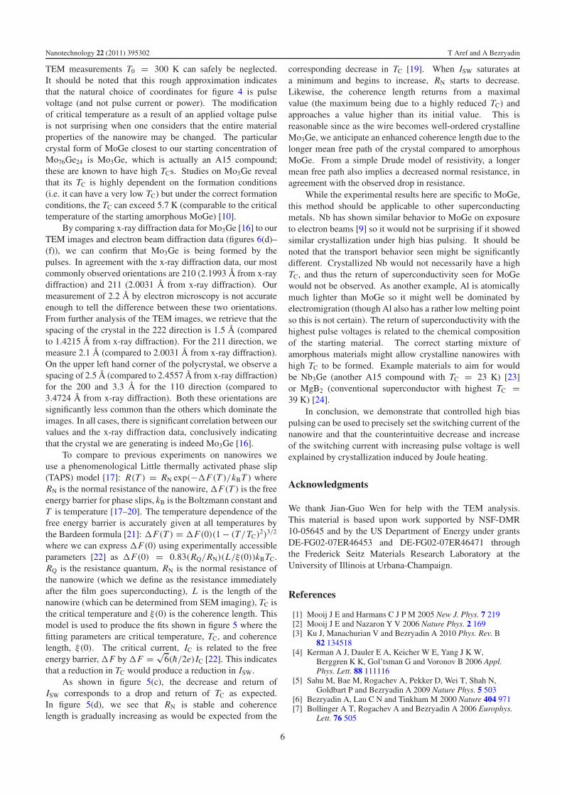
TEM measurements T0 = 300 K can safely be neglected.It should be noted that this rough approximation indicatesthat the natural choice of coordinates for figure 4 is pulsevoltage (and not pulse current or power). The modificationof critical temperature as a result of an applied voltage pulseis not surprising when one considers that the entire materialproperties of the nanowire may be changed. The particularcrystal form of MoGe closest to our starting concentration ofMo76Ge24 is Mo3Ge, which is actually an A15 compound;these are known to have high TCs. Studies on Mo3Ge revealthat its TC is highly dependent on the formation conditions(i.e. it can have a very low TC) but under the correct formationconditions, the TC can exceed 5.7 K (comparable to the criticaltemperature of the starting amorphous MoGe) [10].
By comparing x-ray diffraction data for Mo3Ge [16] to ourTEM images and electron beam diffraction data (figures 6(d)–(f)), we can confirm that Mo3Ge is being formed by thepulses. In agreement with the x-ray diffraction data, our mostcommonly observed orientations are 210 (2.1993 A from x-raydiffraction) and 211 (2.0031 A from x-ray diffraction). Ourmeasurement of 2.2 A by electron microscopy is not accurateenough to tell the difference between these two orientations.From further analysis of the TEM images, we retrieve that thespacing of the crystal in the 222 direction is 1.5 A (comparedto 1.4215 A from x-ray diffraction). For the 211 direction, wemeasure 2.1 A (compared to 2.0031 A from x-ray diffraction).On the upper left hand corner of the polycrystal, we observe aspacing of 2.5 A (compared to 2.4557 A from x-ray diffraction)for the 200 and 3.3 A for the 110 direction (compared to3.4724 A from x-ray diffraction). Both these orientations aresignificantly less common than the others which dominate theimages. In all cases, there is significant correlation between ourvalues and the x-ray diffraction data, conclusively indicatingthat the crystal we are generating is indeed Mo3Ge [16].
To compare to previous experiments on nanowires weuse a phenomenological Little thermally activated phase slip(TAPS) model [17]: R(T ) = RN exp(−�F(T )/kBT ) whereRN is the normal resistance of the nanowire, �F(T ) is the freeenergy barrier for phase slips, kB is the Boltzmann constant andT is temperature [17–20]. The temperature dependence of thefree energy barrier is accurately given at all temperatures bythe Bardeen formula [21]: �F(T ) = �F(0)(1 − (T/TC)2)3/2
where we can express �F(0) using experimentally accessibleparameters [22] as �F(0) = 0.83(RQ/RN)(L/ξ(0))kBTC.RQ is the resistance quantum, RN is the normal resistance ofthe nanowire (which we define as the resistance immediatelyafter the film goes superconducting), L is the length of thenanowire (which can be determined from SEM imaging), TC isthe critical temperature and ξ(0) is the coherence length. Thismodel is used to produce the fits shown in figure 5 where thefitting parameters are critical temperature, TC, and coherencelength, ξ(0). The critical current, IC is related to the freeenergy barrier, �F by �F = √
6(h/2e)IC [22]. This indicatesthat a reduction in TC would produce a reduction in ISW.
As shown in figure 5(c), the decrease and return ofISW corresponds to a drop and return of TC as expected.In figure 5(d), we see that RN is stable and coherencelength is gradually increasing as would be expected from the
corresponding decrease in TC [19]. When ISW saturates ata minimum and begins to increase, RN starts to decrease.Likewise, the coherence length returns from a maximalvalue (the maximum being due to a highly reduced TC) andapproaches a value higher than its initial value. This isreasonable since as the wire becomes well-ordered crystallineMo3Ge, we anticipate an enhanced coherence length due to thelonger mean free path of the crystal compared to amorphousMoGe. From a simple Drude model of resistivity, a longermean free path also implies a decreased normal resistance, inagreement with the observed drop in resistance.
While the experimental results here are specific to MoGe,this method should be applicable to other superconductingmetals. Nb has shown similar behavior to MoGe on exposureto electron beams [9] so it would not be surprising if it showedsimilar crystallization under high bias pulsing. It should benoted that the transport behavior seen might be significantlydifferent. Crystallized Nb would not necessarily have a highTC, and thus the return of superconductivity seen for MoGewould not be observed. As another example, Al is atomicallymuch lighter than MoGe so it might well be dominated byelectromigration (though Al also has a rather low melting pointso this is not certain). The return of superconductivity with thehighest pulse voltages is related to the chemical compositionof the starting material. The correct starting mixture ofamorphous materials might allow crystalline nanowires withhigh TC to be formed. Example materials to aim for wouldbe Nb3Ge (another A15 compound with TC = 23 K) [23]or MgB2 (conventional superconductor with highest TC =39 K) [24].
In conclusion, we demonstrate that controlled high biaspulsing can be used to precisely set the switching current of thenanowire and that the counterintuitive decrease and increaseof the switching current with increasing pulse voltage is wellexplained by crystallization induced by Joule heating.
Acknowledgments
We thank Jian-Guo Wen for help with the TEM analysis.This material is based upon work supported by NSF-DMR10-05645 and by the US Department of Energy under grantsDE-FG02-07ER46453 and DE-FG02-07ER46471 throughthe Frederick Seitz Materials Research Laboratory at theUniversity of Illinois at Urbana-Champaign.
References
[1] Mooij J E and Harmans C J P M 2005 New J. Phys. 7 219[2] Mooij J E and Nazaron Y V 2006 Nature Phys. 2 169[3] Ku J, Manachurian V and Bezryadin A 2010 Phys. Rev. B
82 134518[4] Kerman A J, Dauler E A, Keicher W E, Yang J K W,
Berggren K K, Gol’tsman G and Voronov B 2006 Appl.Phys. Lett. 88 111116
[5] Sahu M, Bae M, Rogachev A, Pekker D, Wei T, Shah N,Goldbart P and Bezryadin A 2009 Nature Phys. 5 503
[6] Bezryadin A, Lau C N and Tinkham M 2000 Nature 404 971[7] Bollinger A T, Rogachev A and Bezryadin A 2006 Europhys.
Lett. 76 505
6

Nanotechnology 22 (2011) 395302 T Aref and A Bezryadin
[8] Aref T, Brenner M and Bezryadin A 2009 Nanotechnology20 045303
[9] Remeika M and Bezryadin A 2005 Nanotechnology 16 1172[10] Ghosh A K and Douglass D H 1977 J. Low Temp. Phys. 27 487[11] Rogachev A and Bezryadin A 2003 Appl. Phys. Lett. 83 512[12] Park H, Lim A, Alivisatos A, Park J and McEuen P 1999 Appl.
Phys. Lett. 75 301[13] Strachan D R, Johnston D E, Guiton B S, Datta S S,
Davies P K, Bonnell D A and Johnson A T C 2008 Phys.Rev. Lett. 100 056805
[14] Heersche H B, Lientschnig G, O’Neill K, van der Zant H andZandbergen H 2007 Appl. Phys. Lett. 91 072107
[15] Holm R 1967 Electrical Contacts (Berlin: Springer)
[16] Searcy A W, Peavler R J and Yearian H J 1952 J. Am. Chem.Soc. 74 566
[17] Bezryadin A 2008 J. Phys.: Condens. Matter 20 043202[18] Chu S L, Bollinger A T and Bezryadin A 2004 Phys. Rev. B
70 214506[19] Tinkham M 1996 Introduction to Superconductivity (New York:
Dover)[20] Langer J S and Ambegaokar V 1967 Phys. Rev. 164 498[21] Bardeen J 1962 Rev. Mod. Phys. 34 667[22] Tinkham M and Lau C N 2002 Appl. Phys. Lett. 80 2946[23] Gavaler J R, Janocko M A and Jones C K 1974 J. Appl. Phys.
45 3009[24] Nagamatsu J, Nakagawa N, Muranaka T, Zenitani Y and
Akimitsu J 2001 Nature 410 63
7