polymer electronic materials: a review of charge transport
TRANSCRIPT

Polymer International Polym Int 55:1371–1384 (2006)
ReviewPolymer electronic materials:a review of charge transportManu Jaiswal and Reghu Menon∗Department of Physics, Indian Institute of Science, Bangalore – 560 012, India
Abstract: This article presents an overview of the charge transport phenomenon in semiconducting polymermaterials. In these disordered systems both intrinsic and extrinsic parameters play significant roles. In general,π-electron delocalization, interchain interaction, band gap, carrier density, extent of disorder, morphology andprocessing of materials determine the electrical and optical properties. The chemical structure, especially therole of side groups, is quite important in both physical and processing properties. The nature of charge carriersand their role in charge transport depend on the structure and morphology of the system. Hence in severalsemiconducting polymer devices, the correlations among structure, morphology and transport are rather strong.The dependence of carrier mobility on temperature and electric field needs to be understood in the frameworkof competing models based on carrier hopping, trapping/detrapping and tunneling. Exactly what determines thedispersive/nondispersive, polaronic and correlative transport regimes is yet to be quantified. An understanding ofthe carrier mobility in semiconducting polymers is necessary to optimize the performance of polymeric electronicdevices. 2006 Society of Chemical Industry
Keywords: polymeric electronics; conjugated polymers; charge transport; mobility; semiconducting behavior;polymeric field-effect transistor; polymeric light-emitting diode
INTRODUCTIONSemiconducting polymers are poised to transform thescenario of today’s electronics and display technology.Intensive research in the last two decades has beenstimulated by the prospect for low-cost fabricationof devices with reasonable stability and performance.Although the field of semiconducting and conductingpolymers has generated a huge amount of literature,the potential for conduction in polymeric materialsitself remained unrecognized for a long time. Inusual saturated carbon-based polymers, which havebeen the focus of research and industry for severaldecades, the electrons are in a bound state andconsequently unavailable for electrical conduction.Conduction with the help of delocalized π-electronsis, however, possible in conjugated polymers. Thesepolymers are characterized by a succession ofconjugated (alternating single and double) bonds.There is one π-orbital perpendicular to the planeof the macromolecule in addition to the in-planeσ -orbitals. The π-electrons are delocalized overseveral carbon atoms in the chain to form π-bands.The presence of an energy gap between the filledand empty bands imparts a semiconducting natureto the polymer instead of a metallic one. Thedelocalized π-electrons are primarily responsible forthe electrical and optical properties in these systems.In 1974, the first semiconducting polymer films wereprepared in the form of polyacetylene (PA); andthree years later, Heeger and co-workers reported the
first electrically conducting organic polymer – iodine-doped trans-PA – whose conductivity of 103 S cm−1
was an increase of seven orders of magnitude overthat of the undoped polymer.1 This discovery wasthe first demonstration of metallic-like conduction bydoping the π-electrons (the dopant iodine removes theelectrons, and the holes in the chain act as carriers: p-type doping) along the polymer chain (although (SN)x
had already been known for a few years),2 and was thesubject of the Nobel Prize in Chemistry in 2000. Oneof the main advantages of using conducting polymersis the fact that photo/chemical/electrochemical dopingcan modify in a controlled way their conductivitiesand Fermi levels.3 Therefore the properties ofsemiconducting polymer devices can be easily tailoredto suit an application; for example, the band gapin these systems can be easily tuned by subtlemodification of the chemical structure.
In the late 1980s, researchers were successful inmaking devices such as thin-film field-effect transistors(FETs),4–8 electroluminescent diodes (light-emittingdiodes, LEDs)5,9,10 and solar cells11,12 from undopedconjugated polymers (shown schematically in Fig. 1).The low cost, ease of processibility and goodmechanical properties make these devices particularlylucrative in the opto-electronics industry. The focus ofresearch on these materials has been to obtain a deviceperformance comparable to that of existing inorganicsemiconductor devices.
∗ Correspondence to: Reghu Menon, Department of Physics, Indian Institute of Science, Bangalore – 560 012, IndiaE-mail: [email protected](Received 31 December 2005; revised version received 31 March 2006; accepted 11 May 2006)Published online 29 August 2006; DOI: 10.1002/pi.2111
2006 Society of Chemical Industry. Polym Int 0959–8103/2006/$30.00

M Jaiswal, R Menon
Figure 1. Typical structures of (a) PFET (b) PLED. Solar cells basedon a blend of donor-type semiconducting polymer with anacceptor-type molecule (e.g. C60) involve a photo-induced chargetransfer, the reverse of the LED process.
The present review focuses on the phenomenon ofcharge transport in undoped conjugated polymer sys-tems. The charge transport scenario in both doped andundoped conjugated polymers is complex on accountof the plethora of intrinsic and extrinsic factors thatinfluence it – including energetic and spatial disor-der, doping, excitations produced by charge–latticeinteractions, inter-/intra-chain interactions, conjuga-tion length, correlations, morphology, interface, etc.The role of these factors in affecting the chargetransport in semiconducting polymers is discussed inthis review (reviews on doped conducting polymershave been published elsewhere13,14). The difficulty inestablishing theoretical models has hindered a holisticunderstanding of the transport mechanism that incor-porates both the macroscopic and the microscopicviewpoints. Mobility is one of the key parameters ofinterest – both towards realizing improved device per-formance, as well as studying the underlying semicon-ductor physics in these materials. The measurement of
low mobility (µ � 1 cm2 V−1 s−1) itself is an intrigu-ing problem. Experimentally, the values of mobilityobtained in polymeric FETs and LEDs show a dif-ference of many orders of magnitude, whereas themobility measurements by various photocarrier gener-ation techniques present different transport scenarios.The unusual statistical mechanics of dispersive trans-port is also observed in these disordered systems. Themechanism of transport in semiconducting polymericmaterials has been the source of much debate, anddiverse models that attempt to explain it include carrierhopping between localized states, polaronic hoppingand trapping/detrapping. Floating empirical parame-ters in these models have often permitted successfulinterpretations from the various possible mechanisms;hence each model tends to interpret some preferreddata set quite well, from a wide variety of measure-ments, to justify the validity of the model.
The ultimate goal of conducting polymer science isto produce materials and devices of higher quality.Towards this end, the study of charge transportphenomena in these materials is indispensable.
MATERIAL STRUCTUREDelocalization of π-electronsThe chemical structure of some important semicon-ducting polymers is shown in Fig. 2. As mentionedabove, the π-electron delocalization along the carbonchains gives rise to interesting electrical and opti-cal properties in conjugated polymers. Consider theexample of PA, which has one of the simplest struc-tures in this class of materials. The π-electron systemis formed by the pz-orbitals of the sp2-hybridized car-bon atoms. Of the four valence electrons of carbon,
Figure 2. Chemical structures of some important semiconducting polymers. The substitutent groups for poly(p-phenylene vinylene) are2-methoxy,5-(3’,7’ -dimethyloctyloxy) (MDMO) and 2-methoxy,5-(2’ ethyl hexyloxy) (MEH).
1372 Polym Int 55:1371–1384 (2006)DOI: 10.1002/pi
Polymer electronic materials: a review
three occupy the strong σ -bonds with two carbons anda hydrogen atom. The fourth valence electron occu-pies the non-hybridized pz-orbital. The overlappingπ-electron wavefunctions together form a π-band.Since the delocalized orbitals are half-filled, one mightexpect metallic behavior on account of finite densityof states (DOS) at the Fermi level. This does nothappen due to the appearance of a band gap betweenthe filled bonding states (π-bands) and empty anti-bonding states (π∗-bands), lowering the energy offilled states on account of Peierls instability.15 ThePeierls theorem states that a one-dimensional system(the long carbon chain in this case) with incompletelyfilled band distorts so as to open up a gap at the Fermilevel.16 The semiconducting state for the polymer istherefore energetically more favorable than the metal-lic one. The energy gap for the conjugated polymers,which is the energy difference between the lowestunoccupied molecular orbital (LUMO) and the high-est occupied molecular orbital (HOMO), varies from0.8 to 4 eV, thereby covering the entire range frominfrared (IR) to ultraviolet (UV), and this also dependson the extent of delocalization of π-electrons. Hence insemiconducting polymers, the band gap, band struc-ture and the delocalization length along the chain areimportant intrinsic parameters that play a major role inthe optical and electrical properties, and consequentlyalso in devices.
Role of intrinsic factorsApart from charge delocalization, the intrinsic factorsimportant to charge transport in conjugated polymersare inter-chain interactions, π –π stacking and therole of side groups. The delocalization of π-electronsalong the polymer backbone alone is not sufficientfor conduction because of inherent localization in aone-dimensional system. It is in this context that thepossibility of inter-chain transfer gathers importance.Even a weak inter-chain coupling can ensure thatthe charge carriers can diffuse across the carbonchains in between scattering events from defects (e.g.sp3 sites, chain ends) and disorder.17 The transferintegral (t⊥) characterizes the inter-chain coupling andis defined as the ratio of electron–phonon couplingto electronic intersite coupling.18,19 The inter-chaincoupling t⊥ represents usually only a small percentage(about 1%) of the on-chain transfer integral t‖18,20,21 to achieve conduction across chains. Anotherimportant ingredient, especially in chains consistingof aromatic rings [e.g. polyparaphenylene (PPP),poly(paraphenylene vinylene) (PPV), etc.], is the chainstiffness and ring-flips that play a major role in thegeneration and lifetimes of primary excitations. Theeffects on physical properties due to ordering, inter-chain coupling and π –π stacking is best illustratedwith the case of regioregularity in alkyl-thiophenepolymers.
Structure, morphology and transportStructure therefore plays a major role in altering thephysical properties of conjugated polymers. It may
also be noted that trans-PA has a slightly betteroverlap and electron delocalization than cis-PA. Asa result, the former has a lower band gap and isa better photoconductor and photocarrier generatorthan cis-PA.22 A crystalline fibrillar morphology isfavored by the compact semi-rigid rod structureof PA.23 The randomly oriented chains can bestretched to increase the ordering of crystallinedomains and to increase the crystalline coherencelength (CCL).23 The anisotropy of CCL contributestowards anisotropic features in electrical and opticalproperties of oriented PA. A hierarchy of length scalesfrom nanoscopic scale in single chains to macroscopicscale in bulk morphology can determine the overalltransport properties. For example, the coiled-up andextended structure of chains can affect the fibrillar andglobular morphologies, and these in turn influenceboth intra- and inter-chain charge transport.
Side groups and regioregularityRegioregularity is the percentage of stereoregularhead-to-tail (HT) attachment of alkyl side-chain to the3-position of thiophene rings.24 High regioregularityis associated with a reduced band gap and enhancedelectrical conductivity,25,26 enhanced mobility27 andphotoconductivity and greater stability and light-generation efficiency in polymer LEDs.28 Enhancedregioregularity leads to increased planarity and quinoidcharacter of neighboring thiophene units in thepolymer backbone.25 It has been shown that enhancedFET mobility of a regioregular (RR) polymer isdetermined by the large mobility anisotropy alongand across the plane of π –π stacking, wherethe former has more efficient inter-chain transportdue to two-dimensional delocalization of carriersin self-ordered stacking lamellae.27 FET mobilitycan then take high values like 0.1 cm2 V−1 s−1.29
These results are consistent with optical spectroscopicexperiments that show delocalization of polarons overseveral polymer chains in RR poly(3-alkyl thiophene)(P3AT).30 The optical transitions carry the signatureof two-dimensional delocalized polarons in contrastto the one-dimensional chain model response. Thisdependence on regioregularity has many advantages,for example the tuning of colors in electrochromicdisplays can be achieved by tuning the regioregularity.Interesting differences in the magnetoresistance (MR)properties have also been recently reported for RRand regiorandom (RRa) films.31 Furthermore, theregioregularity in PPV derivatives has also attractedconsiderable attention from the optical properties anddevice points of view.32
The alkyl group substitution in P3ATs is theclassic example to demonstrate the wide-range tun-ing of the physical properties, and also to influ-ence significantly the processibility of these materi-als. For example, decyl and dodecyl side groups inP3ATs can induce a so-called ‘side group-inducedself-assembly’ while shorter or longer side groupscannot make this self-organization effectively.33,34
Polym Int 55:1371–1384 (2006) 1373DOI: 10.1002/pi

M Jaiswal, R Menon
Figure 3. Efficiency of lamellar stacking and ordering of polymerchains in polyalkylthiophenes depends on the nature of the sidegroups R.
Macromolecular self-assembly is reflected in thehigh conductivity values (∼1000 S cm−1) in HTpoly(3-dodecylthiophene) when compared to HTpoly(3-octylthiophene) (200 S cm−1) and HT poly(3-hexylthiophene) (150 S cm−1).33,34 The lamellar stack-ing in these materials (see Fig. 3) improves theirelectrical and mechanical properties.33,34 Similarly ithas been observed that some special side groups caninduce liquid crystalline-type assembly of the mainchains, and this influences the charge transport to alarge extent.35
Low band-gap polymersThe side groups present in the main chain of apolymer can also significantly alter the electronicproperties. An alkyl group substitution affects thechain alignment, inter-chain interactions and π-electron delocalization and processibility, and canchange the molecular geometry such as the torsionalangle between rings (e.g. in PPV), and these inturn affect the electrical and optical properties.22
The band gap of polyisothionaphthene (PITN) islowered to 1 eV, from the 2 eV value of the parentpolymer, polythiophene (PT).36 This happens dueto an increase in the quinoid character, and isproportional to the resultant bond length alterationalong the polymer backbone. The particular interestin small band-gap polymers originates from theexpected intrinsic conductivity behavior and long-wavelength optical transitions in the visible spectrumof these materials.37 One approach towards achievinga lower band gap is the substitution of alternatingdonor–acceptor units in the polymer backbone.38,39
Low band gaps like 0.92 eV have been achieved byalternating units of quinonoid and benzoid characters
in the polymer main chain.37 Based on the effectof geometry on π-electron structure and allowedexcitation energy of monomer units, it is possible toobtain good theoretical predictions for low band-gapdesigns in polymers.
CHARGE EXCITATIONSBond alternation in conjugated polymers implies thatthe alternating carbon–carbon double and singlebonds are of different lengths. Had this not been thefavored structure, then all bonds would have the samepartial double bond character, and metallic characterdue to long overlap along the main chain would haveresulted, with the presence of free charge carriers. Onthe contrary, lattice dimerization makes the systemmore stable by lowering the total energy, resultingin the opening up of the band gap as in a typicalsemiconducting material.
The excitations associated with charge transport inpolymers include solitons, polarons and bipolarons,which are formed due to chain deformations pro-duced upon addition or removal of charge. The solitonis unique to systems with degenerate ground stateand has been extensively studied for a few repre-sentative systems such as trans-PA40,41 and poly(1,6-heptadiene).18,42 This degenerate ground state isformed by two geometries of polymer units with thesame energy and can be represented by a ‘doublepotential well’. The soliton leads to a break in bondalternation, wherein the bond alternation phase isopposite on the two sides of the soliton.41 When thenumber of conjugated carbons is odd, the unpairedelectron leads to a neutral soliton with spin 1/2.43
The nonbonding orbital corresponding to the soli-ton state occupies a level at the middle of the bandgap. This level can be occupied by a neutral soli-ton or by a positive (negative) charge with spin zeroupon removal (addition) of an electron from the level.The soliton can move without deformation or dis-sipation along the polymer backbone but this doesnot lead to macroscopic-scale charge transport, buta three-dimensional soliton hopping process can leadto conduction in a lightly doped system.44 The shortlength of undisturbed conjugated segments itself lim-its the conductivity along the PA main chain.45 Thisfact is also supported by frequency-dependent con-ductivity studies.46 The soliton is not confined to asingle carbon atom but has a spin/charge width aboutseven times that of the in-chain lattice constant, andan effective mass of 6me.47 However, this interestingspin-charge separated species in PA, which can also begenerated by photoexcitation, is yet to find any usefulapplication in polymer devices.
When the ground state is non-degenerate, as withmost conjugated polymers, the lattice distortion dueto charge addition/removal favors the formation of alocalized charge defect called polaron.48 It is importantto note that the state corresponding to a polaronis localized closer to the band edges and does not
1374 Polym Int 55:1371–1384 (2006)DOI: 10.1002/pi
Polymer electronic materials: a review
lie on top of the valence band as in inorganicsemiconductors. Whereas only a single state appears(at the mid-gap) for a soliton, two localized statesappear in the band gap for the polaron and a reversalof the bond alternation takes place at the polaron.Lattice distortion energy gain can sometimes outweighthe Coulombic repulsion of like-charges and favor theformation of a polaron pair (bipolaron) as comparedto that of two separate polarons along the polymerchain.43 Whereas polaronic conduction involves thetransport of both charge and spin, only the charge istransported by bipolarons.
In conjugated polymers, the carriers can begenerated by chemical doping, charge injection (asin devices) and optical excitation. In high-qualityheavily doped samples, free carrier absorption hasbeen observed, as the typical signature for metallicity,and it is possible to achieve a carrier density of theorder of 1022 cm−3. In the case of carrier injectionfrom metal electrodes, the interface and work functionmatching play a major role. In photo doping, thekinetics of the decay of the intrinsic and primaryexciton species determines the carrier generation.Nevertheless, tuning on the inter-chain processescomplicates the scenario in single-chain models. Forexample, bound polarons can exist as both intra- andinter-chain species; and the usual spin statistics ofsinglet and triplet excitons need not be appropriatedue to the inter-system crossing via some channels.49
CHARGE TRANSPORTThe charge transport in conjugated polymers caninvolve many processes such as:50
(1) Conduction along the polymer backbone.(2) Hopping across chains due to inter-chain interac-
tions.(3) Tunneling between conducting segments that are
separated by less conducting regions, such as thatobserved in doped polymers like PA.
The first two processes are the most relevant for theundoped semiconducting polymers considered in thiswork. Mobility is the most important parameter inunderstanding the transport in such systems.
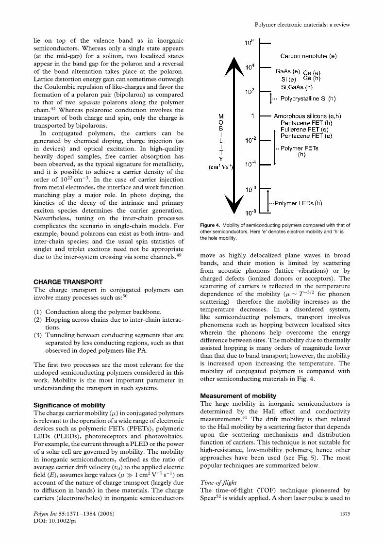
Significance of mobilityThe charge carrier mobility (µ) in conjugated polymersis relevant to the operation of a wide range of electronicdevices such as polymeric FETs (PFETs), polymericLEDs (PLEDs), photoreceptors and photovoltaics.For example, the current through a PLED or the powerof a solar cell are governed by mobility. The mobilityin inorganic semiconductors, defined as the ratio ofaverage carrier drift velocity (vd) to the applied electricfield (E), assumes large values (µ � 1 cm2 V−1 s−1) onaccount of the nature of charge transport (largely dueto diffusion in bands) in these materials. The chargecarriers (electrons/holes) in inorganic semiconductors
Figure 4. Mobility of semiconducting polymers compared with that ofother semiconductors. Here ‘e’ denotes electron mobility and ‘h’ isthe hole mobility.
move as highly delocalized plane waves in broadbands, and their motion is limited by scatteringfrom acoustic phonons (lattice vibrations) or bycharged defects (ionized donors or acceptors). Thescattering of carriers is reflected in the temperaturedependence of the mobility (µ ∼ T−3/2 for phononscattering) – therefore the mobility increases as thetemperature decreases. In a disordered system,like semiconducting polymers, transport involvesphenomena such as hopping between localized siteswherein the phonons help overcome the energydifference between sites. The mobility due to thermallyassisted hopping is many orders of magnitude lowerthan that due to band transport; however, the mobilityis increased upon increasing the temperature. Themobility of conjugated polymers is compared withother semiconducting materials in Fig. 4.
Measurement of mobilityThe large mobility in inorganic semiconductors isdetermined by the Hall effect and conductivitymeasurements.51 The drift mobility is then relatedto the Hall mobility by a scattering factor that dependsupon the scattering mechanisms and distributionfunction of carriers. This technique is not suitable forhigh-resistance, low-mobility polymers; hence otherapproaches have been used (see Fig. 5). The mostpopular techniques are summarized below.
Time-of-flightThe time-of-flight (TOF) technique pioneered bySpear52 is widely applied. A short laser pulse is used to
Polym Int 55:1371–1384 (2006) 1375DOI: 10.1002/pi

M Jaiswal, R Menon
Figure 5. Various types of mobility measurements.
photo-generate charges near one electrode, which driftwithin the material toward the other electrode underan applied electric field. From the decay time (transittime ttr) of the current, the mobility can be obtained asµ = 〈vd〉/E = d2/Vttr, where d is the sample thickness,V the applied voltage and E the corresponding electricfield.
Auston switch techniqueA micro-stripline Auston switch-based picosecondphotoconductivity technique has also been used inplace of TOF. Measurements in a-Se and PPVsuggest possible new implications such as two distincttransport mechanisms:53,54
(1) a short-lived transport involving carrier dynamicsin extended band states until the carrier pro-gressively tunnels into lower states, involving adifferent mobility; and
(2) a long-lived transport in multiple-trapping bandtails with low mobility.
It was also suggested that a built-in potential barrier atmetal–semiconductor interfaces influences the shapeof photocurrent in TOF experiments.53
FET mobilityMobility is also measured using the field effect inPFET devices but the value obtained by this procedureis usually very different from TOF results. Thisis mainly because the thin layer of semiconductoradjacent to the dielectric alone determines the field-effect mobility. The TOF mobility probes the bulkmobility of the sample along a certain direction,whereas the field-effect mobility provides the surfacemobility of the layers adjacent to the gate dielectric.Morphological differences (e.g. depth and profile oftraps) can account for the different mobility values forbulk and surface. The voltage inside the source–drainchannel of the PFET is modeled by taking into accountthe formation of accumulation or depletion layers.The accumulation (depletion) layer corresponds tothe excess (deficit) of majority carriers at the gatedielectric–semiconductor interface upon applicationof a voltage bias, which results in band bending. The
equation is simplified in saturation regime (where thedrain current is independent of drain voltage) and thedrain current is given by
Id,sat = Z2L
µCi(Vg − Vt)2 (1)
where Ci is the dielectric capacitance per unit area, Vg
and Vt are gate and threshold voltages, respectively,and Z and L are the area and length of the channel,respectively.55 The value of µ can be obtained fromEqn (1).
CELIV techniqueA charge extraction by linearly increasing voltage(CELIV) technique has also been applied recentlyfor mobility estimation in RR-P3HT.56 A linearlyincreasing electric field is applied at one electrodeand the current transient is used to obtain thevalue of mobility that arises from ‘doping-induced’charged carriers. The temperature and electric fielddependence of mobility obtained from TOF agreeswell with CELIV mobility indicating that the mode ofcarrier generation (i.e. photo-generation versus doping-induced) has no significant effect.
Photo-induced transient Stark spectroscopyThis technique, recently described, involves anelectrode-less method for obtaining the intrinsicmobility, i.e. mobility not limited by traps anddefects in the material or by recombination.57 Theground state electroabsorption is studied duringcharge separation when photo-induced electron–holepairs are generated. When these carriers drift apart,(i.e. photo-induced polarization takes place) theirdipole nature opposes the electric field, thus leadingto a change in the measured Stark effect. The intrinsiccharge carrier mobility and electron–hole separationcan be inferred from this experiment in the picosecondregime.57 Similar to the results presented by theAuston switch technique (see above), this experimenthas also suggested large intrinsic mobility before thetransition to slower transport takes place, due totrapping and recombination in the nanosecond timescale.
Dependence on temperature and electric fieldMobility has a strong dependence on both temperatureand applied electric field and this is helpful inunderstanding the underlying transport mechanism.Usually, a Poole–Frenkel (PF)-type dependence ofthe mobility on the electric field over an extendedrange is observed (ln µ ∼ SE1/2, where S is theslope parameter).58 This holds true for a largenumber of systems along with other features suchas sign-reversal of the coefficient S at a particulartemperature, deviation from PF law at low electricfields, etc. The PF law arises naturally from the theoryof trapping/detrapping in disordered materials (seebelow).58 The application of electric field results in
1376 Polym Int 55:1371–1384 (2006)DOI: 10.1002/pi

Polymer electronic materials: a review
Figure 6. Potential barrier in the Poole–Frenkel model. Theapplication of an electric field E lowers the potential barrier in thedirection of the field by an amount proportional to E1/2.
a lowering of the potential barrier in the direction ofthe electric field, shown schematically in Fig. 6. Thisfacilitates charge carrier motion from a trapping center.In the presence of an electric field E, the potentialaround a (immobile) positive trapping center (whichtraps/detraps electrons) is given by
�(r) = − q2
4πεr− qE.r (2)
The lowering of the energy barrier58 in the direction ofthe field is then obtained as d�/dr = 0 or �� ∼ E1/2.However, PF-type dependence is also seen in theabsence of traps and this creates the scope forinterpretation of the phenomenon from alternativemodels. Furthermore, a negative field dependencehas been observed in some systems in a range offields, which is contrary to intuition. The temperaturedependence of ln µ has been usually described as 1/T2
but in many cases an Arrhenius-type 1/T dependenceis suggested.
TRANSPORT MODELSThe special case of dispersive systems is describedbelow. Broadly speaking, the transport models thatattempt to describe the observed behavior of mobilityin non-dispersive systems fall into three categories:
(1) Hopping in a Gaussian disorder model (GDM)(2) Polaron transport(3) Trapping/detrapping model
A review by Braun59 gives a tabulated summary of theequations relating to transport arising from the diversemodels.
Hopping in GDMBassler pioneered the Gaussian disorder-based hop-ping model for transport in disordered semiconductingpolymers.60 The DOS is easily determined for inor-ganic semiconductors from optical transitions, from
the valence band (VB) to the conducting energy band(CB). The same approach is difficult to apply for dis-ordered organic systems, as the optical spectra involveexcitonic transitions. Bassler suggested a Gaussianprofile for the DOS based on the observed shapes ofabsorption and fluorescence bands.60 Since the extentof the π-electron delocalization length in the poly-mer main chain is random, there is a fluctuation inthe lattice polarization energy that leads to energeticdisorder.60 This random variation manifests itself inthe Gaussian profile of the DOS, and the transportis assumed to involve charge carrier hopping amonglocalized sites.
The transport of the carriers to adjacent inter-/intra-chain sites is determined by the Miller–Abrahams(M–A) formulation,61 wherein a single phononsupplies the energy for hopping. The transition ratefrom site i to site j separated by a distance �rij is givenby
wij = vo exp(
−2α�rij − �εij
kBT
)for εj > εi
wij = vo exp(−2α�rij) for εj < εi
(3)
Here vo is the attempt frequency and 1/α is thelocalization length (roughly the π-electron delocal-ization length) of the wavefunctions.62 Note that thetemperature-dependent energy barrier is involved onlyfor hops to a higher state. The distance factor �rij isthe expected overlap of the wavefunctions betweenthese two sites. In these disordered materials, hoppingis treated as a percolation-type problem wherein thetransport depends crucially on the ‘most difficult’ hopsbetween clusters, rather than on ‘average hops’; andit is the ‘critical hop’ that completes the otherwisebroken link between clusters. The large numbers ofmodels within this framework rely on this formulationbut differ in their calculations for critical hopping dis-tance and energy. Coehoorn et al.63 compared thesevarious models in detail, a brief summary of which ispresented below. The conductivity σ is estimated inthe Movaghar–Schirmacher model64 by taking contri-butions from all sites; the Vissenberg–Matters model65
uses a percolation treatment involving a critical con-ductance that links up broken clusters to obtain thesame result. The mobility is then obtained, using theexpression µ = σ/ne, where n is the carrier density. Inthe model by Arkhipov et al.66 mobility is computedwith the assumption that the hop from a given sitei takes place to that site j for which the M–A hop-ping rate is the highest. The simplest model is that byMartens et al.,67 which relies on estimating the ‘criti-cal conductivity determining hop distance/energy’, byminimizing the conductivity. Another notable featurein arriving at the mobility is the necessary assumptionthat any site should be multiply connected – this fea-ture is lacking in the models of Martens et al. andArkhipov et al.
The PF law for mobility is valid only in a narrowrange (lower limit 105 V cm−1) in the GDM theory.
Polym Int 55:1371–1384 (2006) 1377DOI: 10.1002/pi
M Jaiswal, R Menon
There is a strong divergence of opinion relatingto the explanation of the experimentally observedextended validity of the PF law. The work ofBassler and models based on his approach do notaccord importance to site correlations. In Bassler’streatment, the underlying assumption for a GaussianDOS is based on the fact that self-energies ofneighboring sites are uncorrelated.60 This is arguedfrom the smallness of structural correlation lengthswhen compared to the large number (∼105) of sitesvisited by a carrier in a ‘real world’ situation. Gartsteinand Conwell68,69 showed the necessity to introduceenergy correlations between sites to account for theobserved extended validity of the PF law (lower limit8 × 103 V cm−1).68,69 The possible sources for suchcorrelations in the randomly fluctuating site energiescould arise from interactions of permanent/transientdipoles or from molecular density fluctuations.68,69 Astrong spatial correlation is shown in the distributionof electrostatic potential in a lattice with randomlyoriented and orientationally uncorrelated dipoles.70
This results from the long-range nature of a dipole’selectrostatic potential. In the treatment of Novikov andco-workers,70–73 the energy fluctuations leading to thePF law arise from random distribution of molecules ina polar medium, as is the case with many molecularlydoped polymers.71 The correlated disorder model(CDM) of Novikov is also based on the M–A hoppingbut the energies of the sites are determined differentlyby summing over the dipole interaction energies. It isthen possible to reconcile to the wider range of validityof the PF law, down to low-to-intermediate fields.Moreover, the GDM assumes a universal M–A rateto arrive at the PF dependence, even for the narrowrange – whereas there is no concrete reason to justifyits universality.
The idea of correlations may hold satisfactorily forpolar materials, but the PF dependence of non-polarmaterials also needs explanation. In this case, theexponent for electric field dependence of mobilityis not exactly 0.5 but is different from it such thatthe PF law can be seen in a limited range.72,73 Aquadrupolar glass (QG) model attempts to explain thecorrelation in non-polar polymers such as PPVs, byconsidering molecules with zero dipole moment buta randomly oriented finite quadrupole moment.72,73
Another model considers the thermal fluctuations ofmolecular geometry (torsional angle of benzene ring)to be the source of energy disorder in non-polarmaterials, in which the steric restoring force bringsabout the site correlation.74
Whereas carriers ‘drift’ along the applied electricfield, diffusion consists of the spread in the carrierpacket due to their unbiased motion in all directionsand accounts for the ‘spread’ in the carrier packetas it drifts under applied field. This is describedby the (generalized) Einstein equation for diffusion.Roichman and Tessler have arrived at chargecarrier density dependence for the modified Einsteinequations.75 This suggests that carrier concentration
plays an important role in the overall mobility ofcarriers.
The mobility of carriers in PLEDs ranges from 10−8
to 10−6 cm2 V−1 s−1, whereas it varies from 10−4 to10−1 cm2 V−1 s−1 for PFETs. Tanase and co-workerstried to unify this (typically) three orders of magnitudedifference in hole mobility by considering the chargecarrier density dependence of mobility.76 Also, asan electric field is applied, there is an increase incarrier injection. It is then difficult to separate outthe effects of electric field and carrier concentration.76
By considering the dependence of mobility on carrierconcentration the explanation for the extended PF lawcan be arrived at without requiring correlation. Thisissue concerning the role of spatial correlation andcarrier concentration is therefore not resolved.
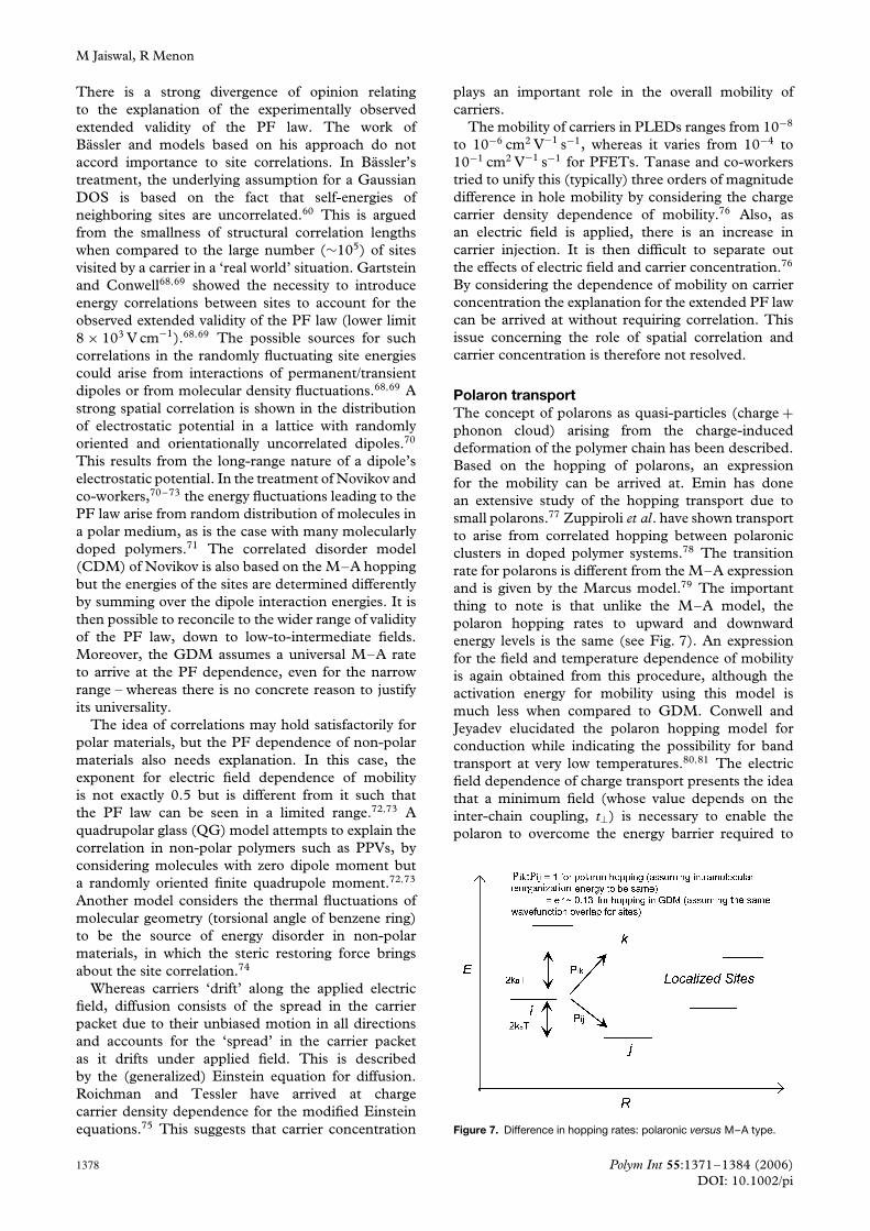
Polaron transportThe concept of polarons as quasi-particles (charge +phonon cloud) arising from the charge-induceddeformation of the polymer chain has been described.Based on the hopping of polarons, an expressionfor the mobility can be arrived at. Emin has donean extensive study of the hopping transport due tosmall polarons.77 Zuppiroli et al. have shown transportto arise from correlated hopping between polaronicclusters in doped polymer systems.78 The transitionrate for polarons is different from the M–A expressionand is given by the Marcus model.79 The importantthing to note is that unlike the M–A model, thepolaron hopping rates to upward and downwardenergy levels is the same (see Fig. 7). An expressionfor the field and temperature dependence of mobilityis again obtained from this procedure, although theactivation energy for mobility using this model ismuch less when compared to GDM. Conwell andJeyadev elucidated the polaron hopping model forconduction while indicating the possibility for bandtransport at very low temperatures.80,81 The electricfield dependence of charge transport presents the ideathat a minimum field (whose value depends on theinter-chain coupling, t⊥) is necessary to enable thepolaron to overcome the energy barrier required to
Figure 7. Difference in hopping rates: polaronic versus M–A type.
1378 Polym Int 55:1371–1384 (2006)DOI: 10.1002/pi

Polymer electronic materials: a review
cross over to another chain.82 A complete polarondelocalization prevents the use of this description atlarger fields.
The role of other excitations such as bipo-larons has also been considered for transportproperties in polymeric transistors. A bipolaronmechanism to explain bias stress in PFETsof RR-polythiophene and poly(9-9′-dioctyl-fluorene-cobithiophene) (F8T2) was suggested.83,84 A gradualdecrease in ‘on current’ of the transistor is seen whenit is turned on for an extended period of time, due tothe depletion of bound hole pairs in the source–drainchannel.
Polaron delocalization and mobilityWohlgennant and co-workers suggested that polarondelocalization is a necessary criterion for highmobility in conjugated polymers.85 This is inferredfrom the optical transition signature of delocalizedpolarons seen in high-mobility polymers like RR-P3HT, methyl-substituted ladder-type poly(para-phenylene) (m-LPPP), and poly(dialkyl-fluorene)(PFO).85 Furthermore, PPV and RRa-P3HT films oflow mobility lack delocalized polarons. As mentionedearlier in the text, the delocalization arises frominter-chain interactions (t⊥ > 0.15 eV).86 Inter-chaininteraction decreases the lattice coupling of the carrierthereby delocalizing it over adjacent chains.85 Sincetwo delocalized polaron energy levels appear in theband gap, the two corresponding optical transitionsare from HOMO to first polaron level (P1) and fromfirst polaron level to second polaron level (P2). Inoligomers, a universal scaling relation exists:
P1 = P1,∞ + constL
(4)
where P1,∞ = transition for infinite-length oligomer.This relation extends to low-mobility polymers, butP1,∞ > P1 for high-mobility polymers with polarondelocalization.85,87
Negative field dependenceThe counter-intuitive negative field dependence in afew systems at low fields has attracted considerableinterest. This behavior has been attributed to thepredominance of diffusion-controlled transport overdrift-controlled transport at low fields.88 Fishchuket al. recently demonstrated the anomalous depen-dence within the paradigm of drift-controlled transportby considering positional disorder, both in Marcus andM–A model frameworks.89 Due to strong positionaldisorder, transport along the electric field may stillinvolve some hops in ‘favorable directions’ which areopposite to the field direction, especially in situationswhere the electronic coupling of the sites is weak inthe field direction. It is these hops that are diminishedby increasing the electric field, leading to a negativefield dependence for mobility.
Trapping/detrappingThe idea of trapping and its limitation has beenintroduced earlier in the text. The transport inorganic LEDs90 and other materials has often beendescribed in the framework of space charge limitedcurrent (SCLC) theory. At low fields, the dominantmechanism is Ohmic conduction, where injectionplays no role due to the metal–semiconductorinterface barrier. As the bias is increased, SCLCconduction follows. This happens when the fielddue to injected carriers itself becomes dominantover that of the applied bias. This reduces thefield at the injecting contact, when the number ofcarriers per unit area inside the sample is equal tothe capacitor charge εεo/e.91 These carriers can betransported per transit time ttr = d/µ, where d is thethickness of the semiconductor. This gives Child’s lawfor trap-free SCLC conduction: jSCL ∝ (εεoµE2)/d.91
The mobility follows from the above relation. Inthe presence of traps, the I –V characteristics aredifferent. Traps are localized levels that immobilizethe charge carriers. They capture electrons/holeswith a probability that follows Fermi–Dirac (FD)statistics.92 A Gaussian DOS distribution is assumedfor HOMO and LUMO states. The deep tail sites ofthese act as continuous pseudo-exponential traps.93,94
Further discrete trapping levels exist in the carrierenergy gap due to chemical impurities and latticedefects.93,94 The injected or existing charges becomeimmobilized (‘trapped’) in the traps, and they arereleased thermally. As detailed in Fig. 8, thermalactivations transfer the carrier from the distributionof trapping centers to the transport band, where theydiffuse for a while until they are trapped again. This isunlike hopping wherein transport takes place betweenthe localized sites themselves. The experimentallyobserved power law form of I –V at higher fields(I ∼ V m, m > 2) follows from SCLC transport in thepresence of an exponential trap distribution.93,94
When all the traps are occupied at still higherfields, the injected charge accumulates near theelectrode, creating a field impeding further chargeinjection.95 Then trap-free SCLC (Child’s law)conduction takes place. Chiguvare and Dyakonovdemonstrated this from the I –V characteris-tics of an ITO/PEDOT/P3HT/Al device.95 Trap-ping/detrapping time scales have been investigatedby pump-probe techniques in polymer LEDs and evi-dence for both deep and shallow traps was found.96
Bussac and Zuppiroli demonstrated the dominanceof space-charge effects for the charge-injection phe-nomenon in the case of polymers with polaroniccarriers and low barrier potentials at the interface.97
It is interesting to note that the mobility in amor-phous silicon is usually interpreted from photocarrierTOF measurements.98 The drift mobility in manysuch systems can be well described by a phenomeno-logical trapping model98,99 that involves a transportedge which separates the DOS into ‘transport’ stateson one side and an exponential band tail (traps) on
Polym Int 55:1371–1384 (2006) 1379DOI: 10.1002/pi
M Jaiswal, R Menon
Figure 8. Energy level diagram illustrating the trapping and releasetransport mechanisms.
the other. The values of mobility for amorphous sili-con are typically higher (∼10 cm2 V−1 s−1) than thoseobserved in disordered semiconducting polymers.
Apart from the PF law dependence seen in theabsence of traps, a few limitations for the trappingmodel merit reference. A very low density of Coulombtraps has been suggested to produce non-dispersive PFtransport but this has not been experimentally detectedso far.72,73 Also the temperature dependence ofmobility (predicted from an equal collection of positiveand negative traps in a correlated energy landscape) istoo strong when compared to experimental data.72,73
The fast transient photoconductivity measurementsin highly ordered PPV (with no side groups) using theAuston switch technique (in place of TOF) indicatethe role of traps after a short-lived transport viaextended bands.100 Picosecond measurements allowa separation of the effects of traps from the intrinsicprocess. The trapping phenomenon is explained by aset of differential equations which yield the trappingtimes and densities. It may be noted, however, thatthe ordered sample had a trap profile and density suchthat µp = µn, whereas most semiconducting polymershave p-type character.
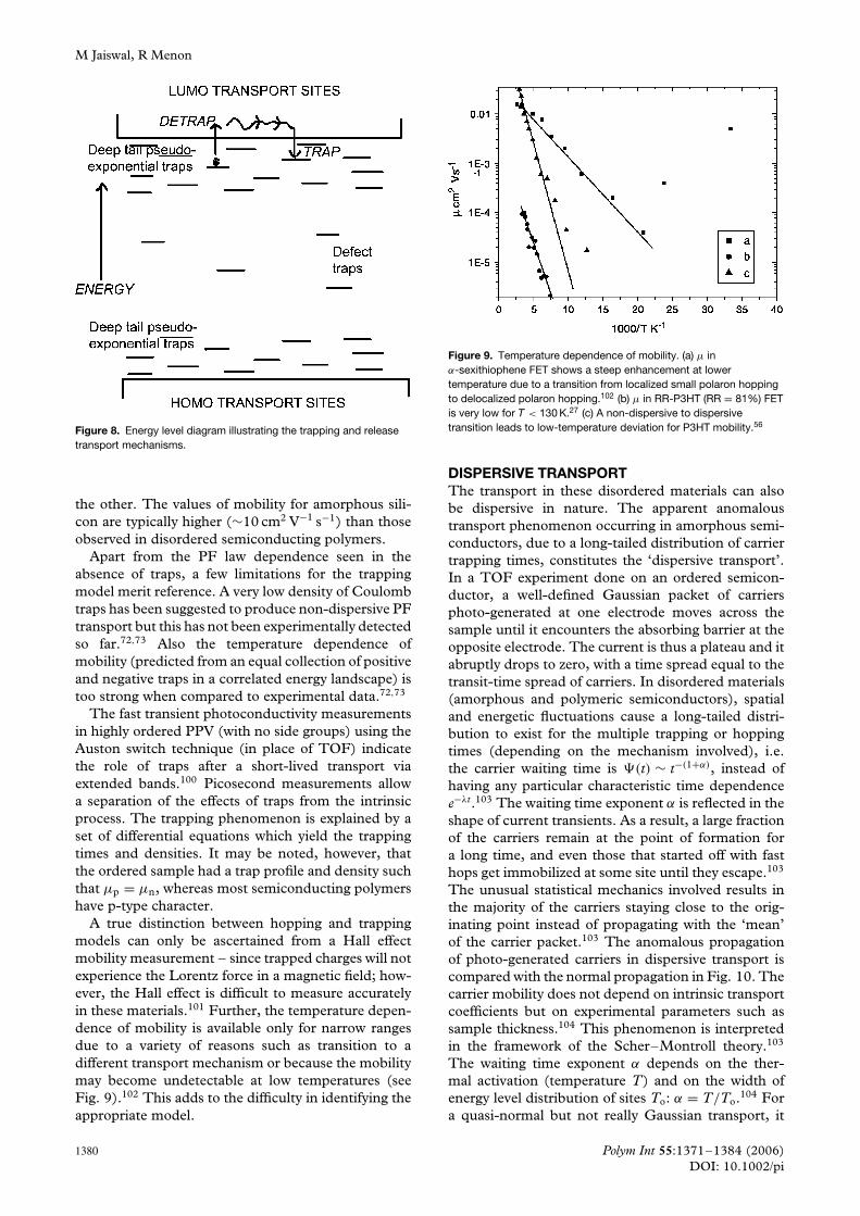
A true distinction between hopping and trappingmodels can only be ascertained from a Hall effectmobility measurement – since trapped charges will notexperience the Lorentz force in a magnetic field; how-ever, the Hall effect is difficult to measure accuratelyin these materials.101 Further, the temperature depen-dence of mobility is available only for narrow rangesdue to a variety of reasons such as transition to adifferent transport mechanism or because the mobilitymay become undetectable at low temperatures (seeFig. 9).102 This adds to the difficulty in identifying theappropriate model.
Figure 9. Temperature dependence of mobility. (a) µ inα-sexithiophene FET shows a steep enhancement at lowertemperature due to a transition from localized small polaron hoppingto delocalized polaron hopping.102 (b) µ in RR-P3HT (RR = 81%) FETis very low for T < 130 K.27 (c) A non-dispersive to dispersivetransition leads to low-temperature deviation for P3HT mobility.56
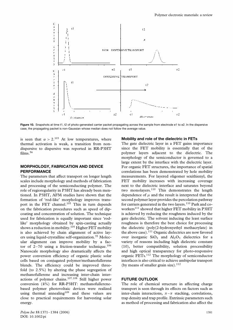
DISPERSIVE TRANSPORTThe transport in these disordered materials can alsobe dispersive in nature. The apparent anomaloustransport phenomenon occurring in amorphous semi-conductors, due to a long-tailed distribution of carriertrapping times, constitutes the ‘dispersive transport’.In a TOF experiment done on an ordered semicon-ductor, a well-defined Gaussian packet of carriersphoto-generated at one electrode moves across thesample until it encounters the absorbing barrier at theopposite electrode. The current is thus a plateau and itabruptly drops to zero, with a time spread equal to thetransit-time spread of carriers. In disordered materials(amorphous and polymeric semiconductors), spatialand energetic fluctuations cause a long-tailed distri-bution to exist for the multiple trapping or hoppingtimes (depending on the mechanism involved), i.e.the carrier waiting time is �(t) ∼ t−(1+α), instead ofhaving any particular characteristic time dependencee−λt.103 The waiting time exponent α is reflected in theshape of current transients. As a result, a large fractionof the carriers remain at the point of formation fora long time, and even those that started off with fasthops get immobilized at some site until they escape.103
The unusual statistical mechanics involved results inthe majority of the carriers staying close to the orig-inating point instead of propagating with the ‘mean’of the carrier packet.103 The anomalous propagationof photo-generated carriers in dispersive transport iscompared with the normal propagation in Fig. 10. Thecarrier mobility does not depend on intrinsic transportcoefficients but on experimental parameters such assample thickness.104 This phenomenon is interpretedin the framework of the Scher–Montroll theory.103
The waiting time exponent α depends on the ther-mal activation (temperature T) and on the width ofenergy level distribution of sites To: α = T/To.104 Fora quasi-normal but not really Gaussian transport, it
1380 Polym Int 55:1371–1384 (2006)DOI: 10.1002/pi
Polymer electronic materials: a review
Figure 10. Snapshots at time t1, t2 of photo-generated carrier packet propagating across the sample from electrode e1 to e2. In the dispersivecase, the propagating packet is non-Gaussian whose median does not follow the average value.
is seen that α > 2.103 At low temperatures, wherethermal activation is weak, a transition from non-dispersive to dispersive was reported in RR-P3HTfilms.56
MORPHOLOGY, FABRICATION AND DEVICEPERFORMANCEThe parameters that affect transport on longer lengthscales include morphology and methods of fabricationand processing of the semiconducting polymer. Therole of regioregularity in P3HT has already been men-tioned. In P3HT, AFM studies have shown that theformation of ‘rod-like’ morphology improves trans-port in the FET channel.105 This in turn dependson the fabrication procedures such as speed of dip-coating and concentration of solution. The techniqueused for fabrication is equally important since ‘rod-like’ morphology obtained by spin-casting actuallyshows a reduction in mobility.105 Higher FET mobilityis also achieved by chain alignment of active lay-ers using liquid-crystalline self-organization.35 Molec-ular alignment can improve mobility by a fac-tor of 2–70 using a friction-transfer technique.106
Nanoscale morphology also dramatically affects thepower conversion efficiency of organic plastic solarcells based on conjugated polymer/methanofullereneblends. The efficiency could be improved three-fold (to 2.5%) by altering the phase segregation ofmethanofullerene and increasing inter-chain inter-actions of polymer chains.107,108 Still higher powerconversion (4%) for RR-P3HT: methanofullerene-based polymer photovoltaic devices were realizedusing thermal annealing109 and these values areclose to practical requirements for harvesting solarenergy.
Mobility and role of the dielectric in FETsThe gate dielectric layer in a FET gains importancesince the FET mobility is essentially that of thepolymer layers adjacent to the dielectric. Themorphology of the semiconductor is governed to alarge extent by the interface with the dielectric layer.For organic FET structures, the importance of spatialcorrelations has been demonstrated by hole mobilitymeasurements. For layered oligomer sexithienyl, theFET mobility increases with increasing coveragenext to the dielectric interface and saturates beyondtwo monolayers.110 This demonstrates the lengthdependence of µ and the result is interpreted that thesecond polymer layer provides the percolation pathwayfor carriers generated in the two layers.110 Park and co-workers111 showed that higher FET mobility in P3HTis achieved by reducing the roughness induced by thegate dielectric. The solvent inducing the least surfaceroughness is therefore the best choice for processingthe dielectric (poly(2-hydroxyethyl methacrylate) inthe above case).111 Organic dielectrics are now favoredover inorganic SiO2 and Al2O3 dielectrics for avariety of reasons including high dielectric constant(10), better compatibility, solution processibilityand high optical transparency for photo-responsiveorganic FETs.112 The morphology of semiconductorinterfaces is also critical to achieve ambipolar transport(by means of smaller grain size).112
FUTURE OUTLOOKThe role of chemical structure in affecting chargetransport is seen through its effects on factors such asinter-chain interactions, π –π stacking, correlations,trap density and trap profile. Extrinsic parameters suchas method of processing and fabrication also affect the
Polym Int 55:1371–1384 (2006) 1381DOI: 10.1002/pi
M Jaiswal, R Menon
transport on larger length scales. While it is desirableto achieve optimum transport properties for polymerelectronic materials, the processibility and fabricationare usually adversely affected as a result. Ideally, thereshould be a compromise between transport propertiesand ease of fabrication so as to have the best economicviability. Polymer FETs have possible applicationssuch as in flexible displays and smart cards. Althougha mobility higher than 0.01 cm2 V−1 s−1 is required forsuch purposes, it need not be comparable to that ofamorphous silicon (10 cm2 V−1 s−1). A mobility suchas 0.1 cm2 V−1 s−1 is sufficient for many applicationsas long as ease of processibility, facile fabricationand stability requirements are fulfilled. Integratedoptoelectronic and all-polymeric devices based onpolymer FET–LED combination have been realizedby improving the mobility and ON-OFF ratio ofFETs.29,113 Low-cost all-polymer integrated circuits(ICs) can be inkjet printed directly from electronicinks and this can replace the involved process ofvacuum deposition and photolithography patterningrequired for inorganic ICs. The main challenge hereis to obtain higher mobilities and switching times inFETs by restricting the spread (statistical variation) ofdrops of solution on the substrate to less than 10 µm.114
Polymeric LEDs have already reached efficienciesthat permit commercialization.115,116 Prins et al.suggested very high intra-chain mobility for ladder-type polymers, so these can be considered as importantcandidates for interconnecting wires in molecularelectronics.117 Furthermore, the higher mobility andstability in n-type polymeric semiconductors, andambipolar characteristics, are yet to be realized,especially at sufficiently low operating voltages. Whatreally limits the mobility of electrons, with respectto holes, is yet to be understood in detail. A facileway to alter the HOMO–LUMO levels to match thework function of carrier-injecting electrodes has notbeen sufficiently explored. Further enhancement ofthe mobility of both carriers is required to improvethe collection efficiency in solar cells, photodiodes,etc. Towards these goals, the chemical structure,self-organization and processibility of semiconductingpolymeric materials are yet to be optimized to attainthe desired transport properties.
CONCLUSIONSDevice performance depends largely on the efficiencyof charge transport processes. Intrinsic factors suchas the structure and ordering of chains, as wellas extrinsic factors like fabrication procedure affectthe transport parameters. In this work, a briefsummary of the diverse charge transport modelshas been presented. Mobility and its dependence onparameters like electric field and temperature usuallycharacterize transport. Presently, models are able toexplain the observed experimental properties to a largeextent, although important theoretical considerations,including the true underlying mechanism, remain
unresolved. Experimental data for non-dispersivetransport are generally available only over a narrowtemperature range so that data are always open toa successful interpretation from both hopping andtrapping models, in the absence of a priori knowledgeabout the transport mechanism.
ACKNOWLEDGEMENTOne of the authors (M. J.) thanks CSIR, New Delhifor financial support.
REFERENCES1 Chiang CK, Fincher Jr. CR, Park YW, Heeger AJ, Shi-
rakawa H, Louis EJ, et al, Phys Rev Lett 39:1098 (1977).2 Walatka Jr. VV, Labes MM and Perlstein JH, Phys Rev Lett
31:1139 (1973).3 Koezuka H, Tsumura A and Ando T, Synth Met 18:699
(1987).4 Assadi A, Svensson C, Willander M and Inganas O, Appl Phys
Lett 53:195 (1988).5 Forrest S, Burrows P and Thompson M, IEEE Spectrum 37:29
(2000).6 Dimitrakopoulos CD and Malenfant PRL, Adv Mater 14:99
(2002).7 Kuo C-T and Chiou W-H, Synth Met 88:23 (1997).8 Fuchigami H, Tsumura A and Koezuka H, Appl Phys Lett
63:1372 (1993).9 Friend RH, Gymer RW, Holmes AB, Burroughes JH,
Marks RN, Taliani C, et al, Nature 397:121 (1999).10 Moliton A, Optoelectronics of Molecules and Polymers (Springer
Series in Optical Sciences, Vol. 104). Springer, New York(2005).
11 Sariciftci NS, Smilowitz L, Heeger AJ and Wudl F, Science258:1474 (1992).
12 Hoppe H and Sariciftci NS, J Mater Res 19:1924 (2004).13 Kiebooms R, Menon R and Lee KH, in Handbook of Advanced
Electronic and Photonic Materials and Devices, Vol. 8, ed. byNalwa HS. Academic Press, San Diego, CA (2001).
14 Menon R, in Handbook of Polymers in Electronics, ed. byMalhotra BD. Rapra Technology Ltd, UK (2002).
15 Heeger AJ, Rev Mod Phys 73:681 (2001).16 Hoffmann R, Janiak C and Kollmar C, Macromolecules 24:3725
(1991).17 Heeger AJ, Faraday Discuss Chem Soc 88:203 (1989).18 Malhotra BD and Saxena V, in Handbook of Polymers in
Electronics, ed. by Malhotra BD. Rapra Technology Ltd,UK (2002).
19 Cornil J, Beljonne D, Calbert JP and Bredas JL, Adv Mater13:1053 (2001).
20 Gartstein YN and Zakhidov AA, Solid State Commun 60:105(1986).
21 da Costa PG, Dandrea RG and Conwell EM, Phys Rev B47:1800 (1993).
22 Menon R and Mukherjee AK, in Electronic and Optical propertiesof Conjugated Molecular Systems in Condensed Phases, ed. byHotta S. Research Signpost, Trivandrum (2003).
23 Tsukamoto J, Adv Phys 41:509 (1992).24 McCullough RD, Adv Mater 10:93 (1998).25 Chen TA and Rieke RD, Synth Met 60:175 (1993).26 McCullough RD and Lowe RD, J Chem Soc Chem Commun
1:70 (1992).27 Sirringhaus H, Brown PJ, Friend RH, Nielsen MM, Bech-
gaard K, Langeveld-Voss BMW, et al, Nature 401:685(1999).
28 Chen F, Mehta PG, Takiff L and McCullough RD, J MaterChem 6:1763 (1996).
29 Sirringhaus H, Tessler N and Friend RH, Science 280:1741(1998).
1382 Polym Int 55:1371–1384 (2006)DOI: 10.1002/pi

Polymer electronic materials: a review
30 Osterbacka R, An CP, Jiang XM and Vardeny ZV, Science287:839 (2000).
31 Mermer O, Veeraraghavan G, Francis TL, Sheng Y,Nguyen DT, Wohlgenannt M, et al, Phys Rev B 72:205202(2005).
32 Munters T, Physio-chemical, electrical and optical propertiesof regiorandom and regioregular MDMO-PPV, PhD thesis,Limburgs Universitair Centrum (2004).
33 McCullough RD and Ewbank PC, in Handbook of ConductingPolymers, ed. by Skotheim TA, Elsenbaumer RL andReynolds JR. Marcel Dekker, New York (1998).
34 McCullough RD, Tristram-Nagle S, Williams SP, Lowe RDand Jayaraman M, J Am Chem Soc 115:4910 (1993).
35 Sirringhaus H, Wilson RJ, Friend RH, Inbasekaran M, Wu W,Woo EP, et al, Appl Phys Lett 77:406 (2000).
36 Bredas JL, Heeger AJ and Wudl F, J Chem Phys 85:4673(1986).
37 Pomerantz M, Gu X and Zhang SX, Macromolecules 34:1817(2001).
38 van Mullekom HAM, Vekemans JAJM and Meijer EW, ChemEur J 4:1235 (1998).
39 Ajayaghosh A, Chem Soc Rev 32:181 (2003).40 Su WP, Schrieffer JR and Heeger AJ, Phys Rev B 22:2099
(1980).41 Su WP, Schrieffer JR and Heeger AJ, Phys Rev Lett 42:1698
(1979).42 Pakbaz K, Wu R, Wudl F and Heeger AJ, J Chem Phys 99:590
(1993).43 Bredas JL and Street GB, Acc Chem Res 18:309 (1985).44 Kaiser AB, Rep Prog Phys 64:1 (2001).45 Curran S, Stark-Hauser A and Roth S, in Handbook of Organic
Conductive Molecules and Polymers, Vol. 2, ed. by Nalwa HS.John Wiley & Sons, Chichester, UK (1997).
46 Menon R, in Handbook of Organic Conductive Molecules andPolymers, Vol. 4, ed. by Nalwa HS. John Wiley & Sons,Chichester, UK (1997).
47 Kivelson S, Phys Rev Lett 46:1344 (1981).48 Fesser K, Bishop AR and Campbell DK, Phys Rev B 27:4804
(1983).49 Lee MK, Segal M, Soos ZG, Shinar J and Baldo MA, Phys Rev
Lett 94:137403 (2005).50 Ehinger K and Roth S, in Electronic Properties of Polymers
and Related Compounds (Solid State Sciences Series 63), ed.by Kuzmany H, Mehring M and Roth S. Springer Verlag,Berlin (1985).
51 Hamaguchi C, Basic Semiconductor Physics. Springer, NewDelhi, p. 263 (2001).
52 Spear WE, J Non-Cryst Solids 1:197 (1969).53 Moses D, Phys Rev B 53:4462 (1996).54 Moses D, Solid State Commun 69:721 (1989).55 Horowitz G, in Semiconducting Polymers: Chemistry, Physics and
Engineering, ed. by Hadziioannou G and van Hutten PF.Wiley-VCH, Weinheim (2000).
56 Mozer AJ, Sariciftci NS, Pivrikas A, Osterbacka R, Juska G,Brassat L et al, Phys Rev B 71:035214 (2005).
57 Cabanillas-Gonzalez J, Virgili T, Gambetta A, Lanzani G,Anthopoulos TD and de Leeuw DM, Phys Rev Lett96:106601 (2006).
58 Kao KC and Hwang W, Electrical Transport in Solids. PergamonPress, Oxford, pp. 314–316 (1981).
59 Braun D, J Polym Sci B 41:2622 (2003).60 Bassler H, Phys Stat Sol (b) 175:15 (1993).61 Miller A and Abrahams E, Phys Rev 120:745 (1960).62 Pasveer WF, Bobbert PA, Huinink HP and Michels MAJ, Phys
Rev B 72:174204 (2005).63 Coehoorn R, Pasveer WF, Bobbert PA and Michels MAJ, Phys
Rev B 72:155206 (2005).64 Movaghar B and Schirmacher W, J Phys C 14:859 (1981).65 Vissenberg MCJM and Matters M, Phys Rev B 57:12964
(1998).66 Arkhipov VI, Heremans P, Emelianova EV, Adriaenssens GJ
and Bassler H, J Phys: Condens Matter 14:9899 (2002).
67 Martens HCF, Hulea IN, Romijn IG, Brom HB, Pasveer WFand Michels MAJ, Phys Rev B 67:121203(R) (2003).
68 Gartstein YN and Conwell EM, Chem Phys Lett 245:351(1995).
69 Dunlap DH, Parris PE and Kenkre VM, Phys Rev Lett 77:542(1996).
70 Novikov SV and Vannikov AV, J Phys Chem 99:14573 (1995).71 Novikov SV, Dunlap DH, Kenkre VM, Parris PE and Van-
nikov AV, Phys Rev Lett 81:4472 (1998).72 Novikov SV, J Polym Sci B 41:2584 (2003).73 Novikov SV, Dunlap DH and Kenkre VM, Proc SPIE
3471:181 (1998).74 Yu ZG, Smith DL, Saxena A, Martin RL and Bishop AR, Phys
Rev Lett 84:721 (2000).75 Roichman Y and Tessler N, Appl Phys Lett 80:1948 (2002).76 Tanase C, Meijer EJ, Blom PWM and de Leeuw DM, Phys
Rev Lett 91:216601 (2003).77 Emin D, in Handbook of Conducting Polymers, ed. by
Skotheim TA. Marcel Dekker, New York (1986).78 Zuppiroli L, Bussac MN, Paschen S, Chauvet O and Forro L,
Phys Rev B 50:5196 (1994).79 Marcus RA, Rev Mod Phys 65:599 (1993).80 Jeyadev S and Conwell EM, Synth Met 28:D439 (1989).81 Conwell EM, Choi HY and Jeyadev S, Synth Met 49:359
(1992).82 Stafstrom S, Hansson A and Johansson A, Synth Met 137:1397
(2003).83 Salleo A and Street RA, Phys Rev B 70:235324 (2004).84 Street RA, Salleo A and Chabinyc ML, Phys Rev B 68:085316
(2003).85 Wohlgenannt M, Jiang XM and Vardeny ZV, Phys Rev B
69:241204(R) (2004).86 Blackman JA and Sabra MK, Phys Rev B 47:15437 (1993).87 Wohlgenannt M, Phys Stat Sol (a) 201:1188 (2004).88 Cordes H, Baranovskii SD, Kohary K, Thomas P, Yamasaki S,
Hensel F et al, Phys Rev B 63:094201 (2001).89 Fishchuk II, Kadashchuk A, Bassler H and Abkowitz M, Phys
Rev B 70:245212 (2004).90 Malliaras GG and Friend RH, Phys Today 58:53 (2005).91 Bassler H, in Semiconducting Polymers: Chemistry, Physics and
Engineering, ed. by Hadziioannou G and van Hutten PF.Wiley-VCH, Weinheim (2000).
92 Kao KC and Hwang W, Electrical Transport in Solids. PergamonPress, Oxford p. 148 (1981).
93 Campbell AJ, Bradley DDC and Lidzey DG, J Appl Phys82:6326 (1997).
94 Campbell AJ, Weaver MS, Lidzey DG and Bradley DDC,J Appl Phys 84:6737 (1998).
95 Chiguvare Z and Dyakonov V, Phys Rev B 70:235207 (2004).96 Yakimov AV, Savvate’ev VN and Davidov D, Synth Met
115:51 (2000).97 Bussac MN and Zuppiroli L, Phys Rev B 55:15587 (1997).98 Schiff EA, J Phys: Condens Matter 16:S5265 (2004).99 Tiedje T, Cebulka JM, Morel DL and Abeles B, Phys Rev Lett
46:1425 (1981).100 Soci C, Moses D, Xu Q-H and Heeger AJ, Phys Rev B
72:245204 (2005).101 Meijer EJ, Charge transport in disordered organic field-effect
transistors, PhD thesis, Delft University of Technology(2003).
102 Torsi L, Dodabalapur A, Rothberg LJ, Fung AWP andKatz HE, Science 272:1462 (1996).
103 Scher H and Montroll EW, Phys Rev B 12:2455 (1975).104 Scher H, Shlesinger MF and Bendler JT, Phys Today 44:26
(1991).105 Wang G, Hirasa T, Moses D and Heeger AJ, Synth Met
146:127 (2004).106 Nagamatsu S, Tanigaki N, Yoshida Y, Takashima W, Yase K
and Kaneto K, Synth Met 137:923 (2003).107 Shaheen SE, Brabec CJ, Sariciftci NS, Padinger F, Fromherz T
and Hummelen JC, Appl Phys Lett 78:841 (2001).108 Brabec CJ, Sariciftci NS and Hummelen JC, Adv Funct Mater
11:15 (2001).
Polym Int 55:1371–1384 (2006) 1383DOI: 10.1002/pi
M Jaiswal, R Menon
109 Li G, Shrotriya V, Yao Y and Yang Y, J Appl Phys 98:043704(2005).
110 Dinelli F, Murgia M, Levy P, Cavallini M, Biscarini F and deLeeuw DM, Phys Rev Lett 92:116802 (2004).
111 Park J, Park SY, Shim SO, Kang H and Lee HH, Appl PhysLett 85:3283 (2004).
112 Singh ThB, Meghdadi F, Gunes S, Marjanovic N, Horowitz G,Lang P, et al, Adv Mater 17:2315 (2005).
113 Gelinck GH, Geuns TCT and de Leeuw DM, Appl Phys Lett77:1487 (2000).
114 Sirringhaus H, Kawase T, Friend RH, Shimoda T,Inbasekaran M, Wu W et al, Science 290:2123 (2000).
115 Service RF, Science 310:1762 (News Focus) (2005).116 Sun Y, Giebink NC, Kanno H, Ma B, Thompson ME and
Forrest SR, Nature 440:845 (2006).117 Prins P, Grozema FC, Schins JM, Patil S, Scherf U and
Siebbeles LDA, Phys Rev Lett 96:146601 (2006).
1384 Polym Int 55:1371–1384 (2006)DOI: 10.1002/pi