photonic integrated circuits at infinera - 7 pennies · pdf filephotonic integrated circuits...
TRANSCRIPT

1 | © 2016 Infinera
Photonic Integrated Circuits at Infinera
Fred Kish
SVP, Optical Integrated Components Group
22 March 2016
2 | © 2016 Infinera
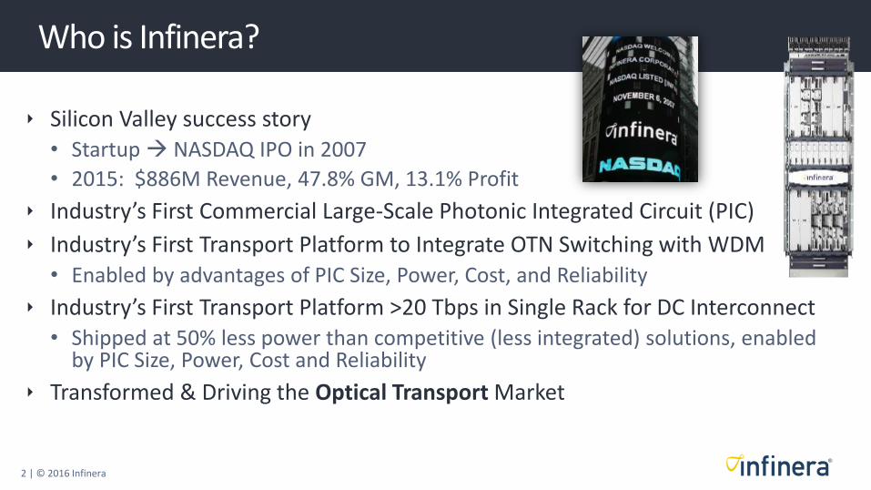
Who is Infinera?
Silicon Valley success story • Startup NASDAQ IPO in 2007
• 2015: $886M Revenue, 47.8% GM, 13.1% Profit
Industry’s First Commercial Large-Scale Photonic Integrated Circuit (PIC)
Industry’s First Transport Platform to Integrate OTN Switching with WDM• Enabled by advantages of PIC Size, Power, Cost, and Reliability
Industry’s First Transport Platform >20 Tbps in Single Rack for DC Interconnect• Shipped at 50% less power than competitive (less integrated) solutions, enabled
by PIC Size, Power, Cost and Reliability
Transformed & Driving the Optical Transport Market
3 | © 2016 Infinera
Why Use Photonic Integration?
$ / Gbps
Watts / Gbps
mm3 / Gbps and mm2 / Gbps
At both component andsystem/network level
Use unique system-level advantages:
Super-channels with sliceability
Instant Bandwidth
Integrated OTN/WDM Switching
4 | © 2016 Infinera
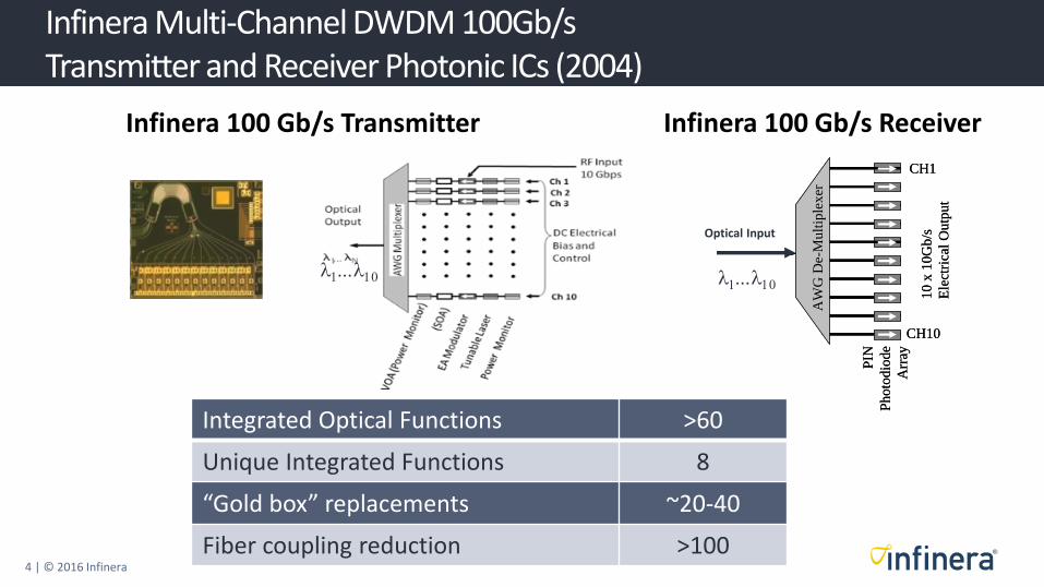
Infinera Multi-Channel DWDM 100Gb/s Transmitter and Receiver Photonic ICs (2004)
Integrated Optical Functions >60
Unique Integrated Functions 8
“Gold box” replacements ~20-40
Fiber coupling reduction >100
Infinera 100 Gb/s Transmitter Infinera 100 Gb/s Receiver10 x 10Gb/s
Electrical Input
Optical
Output
1... 10
10 x 10Gb/s
AW
G M
ult
iple
xer
CH1
CH10
DC
Ele
ctri
cal
Bia
s an
d C
ontr
ol
VO
A A
rray
EA
M A
rray
OP
M A
rray
Tunab
le D
FB
Arr
ay
Optical
Input
CH1
CH10
PIN
Photo
dio
de
Arr
ay
AW
G D
e-M
ult
iple
xer
10 x
10G
b/s
Ele
ctri
cal
Outp
ut
10 x 10Gb/s
Electrical Input
Optical
Output
1... 10
10 x 10Gb/s
AW
G M
ult
iple
xer
CH1
CH10
DC
Ele
ctri
cal
Bia
s an
d C
ontr
ol
VO
A A
rray
EA
M A
rray
OP
M A
rray
Tunab
le D
FB
Arr
ay
Optical
Input
CH1
CH10
PIN
Photo
dio
de
Arr
ay
AW
G D
e-M
ult
iple
xer
10 x
10G
b/s
Ele
ctri
cal
Outp
ut
1...10
Optical Input
1...10
5 | © 2016 Infinera
Why Use InP for Photonic Integration?
Platform capable of highest performance no compromises vs. discrete for ULH, LH, Metro Regional/Core Markets
Platform capable of integration of lasers and gain anywhere in circuit
Converge multiple devices onto single manufacturing platform
Leverage semiconductor learning curve
Platform scalable (build generation upon generation)
6 | © 2016 Infinera
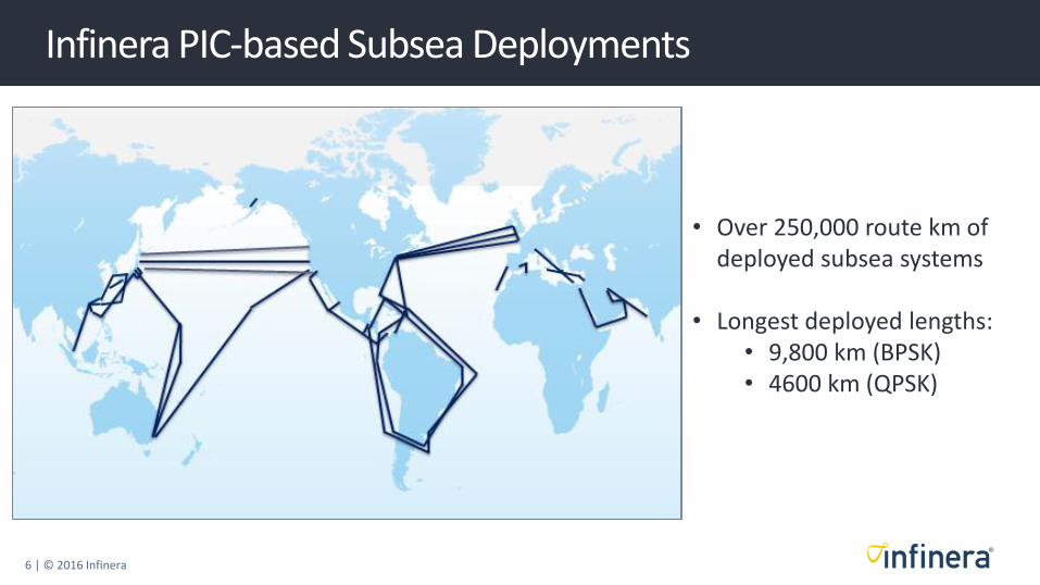
Infinera PIC-based Subsea Deployments
• Over 250,000 route km of deployed subsea systems
• Longest deployed lengths:• 9,800 km (BPSK)• 4600 km (QPSK)
7 | © 2016 Infinera
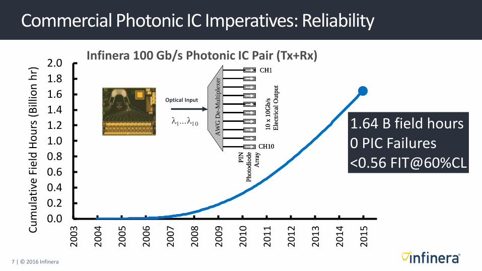
Commercial Photonic IC Imperatives: Reliability
0.0
0.2
0.4
0.6
0.8
1.0
1.2
1.4
1.6
1.8
2.02
00
3
20
04
20
05
20
06
20
07
20
08
20
09
20
10
20
11
20
12
20
13
20
14
20
15Cu
mu
lati
ve F
ield
Ho
urs
(B
illio
n h
r)
1.64 B field hours 0 PIC Failures<0.56 FIT@60%CL
Infinera 100 Gb/s Photonic IC Pair (Tx+Rx)10 x 10Gb/s
Electrical Input
Optical
Output
1... 10
10 x 10Gb/s
AW
G M
ult
iple
xer
CH1
CH10
DC
Ele
ctri
cal
Bia
s an
d C
ontr
ol
VO
A A
rray
EA
M A
rray
OP
M A
rray
Tunab
le D
FB
Arr
ay
Optical
Input
CH1
CH10
PIN
Photo
dio
de
Arr
ay
AW
G D
e-M
ult
iple
xer
10 x
10G
b/s
Ele
ctri
cal
Outp
ut
10 x 10Gb/s
Electrical Input
Optical
Output
1... 10
10 x 10Gb/s
AW
G M
ult
iple
xer
CH1
CH10
DC
Ele
ctri
cal
Bia
s an
d C
ontr
ol
VO
A A
rray
EA
M A
rray
OP
M A
rray
Tunab
le D
FB
Arr
ay
Optical
Input
CH1
CH10
PIN
Photo
dio
de
Arr
ay
AW
G D
e-M
ult
iple
xer
10 x
10G
b/s
Ele
ctri
cal
Outp
ut
1...10
Optical Input
8 | © 2016 Infinera
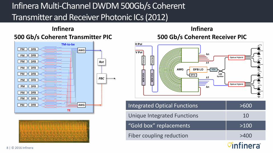
Infinera Multi-Channel DWDM 500Gb/s Coherent Transmitter and Receiver Photonic ICs (2012)
Infinera 500 Gb/s Coherent Transmitter PIC
Infinera500 Gb/s Coherent Receiver PIC
Integrated Optical Functions >600
Unique Integrated Functions 10
“Gold box” replacements >100
Fiber coupling reduction >400
9 | © 2016 Infinera
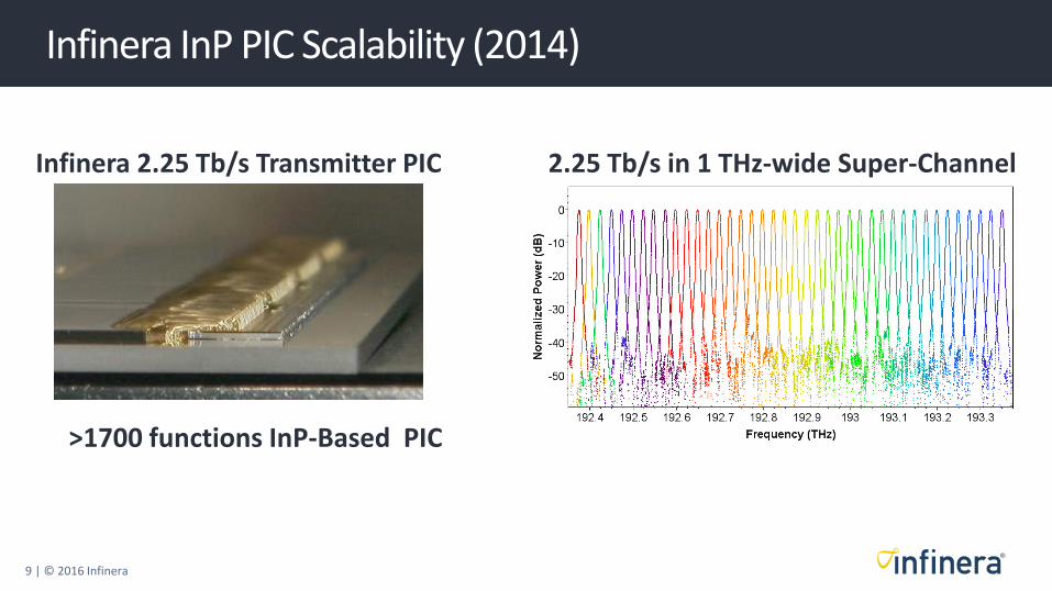
Infinera InP PIC Scalability (2014)
>1700 functions InP-Based PIC
Infinera 2.25 Tb/s Transmitter PIC 2.25 Tb/s in 1 THz-wide Super-Channel

10 | © 2016 Infinera
Infinera’s World Leading Bandwidth Scaling (Per Module Pair)
11 | © 2016 Infinera
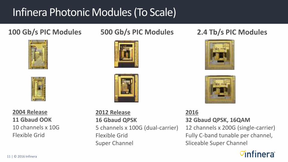
Infinera Photonic Modules (To Scale)
500 Gb/s PIC Modules100 Gb/s PIC Modules 2.4 Tb/s PIC Modules
201632 Gbaud QPSK, 16QAM12 channels x 200G (single-carrier)Fully C-band tunable per channel, Sliceable Super Channel
2004 Release11 Gbaud OOK10 channels x 10GFlexible Grid
2012 Release16 Gbaud QPSK5 channels x 100G (dual-carrier)Flexible GridSuper Channel
12 | © 2016 Infinera
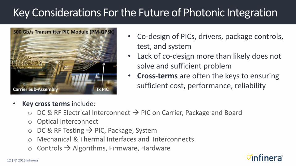
Key Considerations For the Future of Photonic Integration
• Co-design of PICs, drivers, package controls, test, and system
• Lack of co-design more than likely does not solve and sufficient problem
• Cross-terms are often the keys to ensuring sufficient cost, performance, reliability
• Key cross terms include:o DC & RF Electrical Interconnect PIC on Carrier, Package and Boardo Optical Interconnecto DC & RF Testing PIC, Package, Systemo Mechanical & Thermal Interfaces and Interconnectso Controls Algorithms, Firmware, Hardware

13 | © 2016 Infinera