phase-change memory: an architectural perspectivecnfolio.com/media/phase_change_memory.pdf · 29...
TRANSCRIPT

29
Phase-Change Memory: An Architectural Perspective
OMER ZILBERBERG, SHLOMO WEISS, and SIVAN TOLEDO, Tel-Aviv University
This article surveys the current state of phase-change memory (PCM) as a nonvolatile memory technologyset to replace flash and DRAM in modern computerized systems. It has been researched and developed inthe last decade, with researchers providing better architectural designs which address the technology’s mainchallenges—its limited write endurance, potential long latency, high energy writes, power dissipation, andsome concerns for memory privacy. Some physical properties of the technology are also discussed, providinga basis for architectural discussions. Also briefly shown are other architectural alternatives, such as FeRAMand MRAM. The designs surveyed in this article include read before write, wear leveling, write cancellation,write pausing, some encryption schemes, and buffer organizations. These allow PCM to stand on its own asa replacement for DRAM as main memory. Designs for hybrid memory systems with both PCM and DRAMare also shown and some designs for SSDs incorporating PCM.
Categories and Subject Descriptors: C.1 [Computer Systems Organization]: Processor Architectures
General Terms: Design, Performance
Additional Key Words and Phrases: Computer architecture, phase change memory, main memory, hybridmemory systems
ACM Reference Format:Zilberberg, O., Weiss, S., and Toledo, S. 2013. Phase-change memory: An architectural perspective. ACMComput. Surv. 45, 3, Article 29 (June 2013), 33 pages.DOI: http://dx.doi.org/10.1145/2480741.2480746
1. INTRODUCTION
The purpose of this architectural survey is to provide newcomers to the field of PCMresearch with an introduction to PCM, its applications and challenges, and some keyideas already published by researchers. It also provides veteran researchers with aquick index of PCM architectural designs—all researchers affiliated with PCM maybenefit from this article as a quick reference to other, more extensive works focusingon a desired aspect of PCM.
There are quite a few published surveys regarding PCM. Some offer only a glimpseof the current state of PCM development [Atwood 2010; Lai 2003; Lam 2007], whileothers offer a more extensive review of PCM technology [Burr et al. 2010; Li and Lam2011; Ohta 2011; Wong et al. 2010]. However, these surveys mostly cover the physicalproperties of the PCM cell, such as the crystallization process of the chalcogenide glass,fabrication challenges, and the resistivity and endurance of the PCM. To the best ofour knowledge, this is the first survey to cover architectural aspects of incorporatingPCM in common applications, such as PCs, laptops, and SSDs.
Corresponding author’s address: S. Weiss, Department of Electrical Engineering - Systems, Tel-AvivUniversity, Tel-Aviv, 69978, Israel; email: [email protected] to make digital or hard copies of part or all of this work for personal or classroom use is grantedwithout fee provided that copies are not made or distributed for profit or commercial advantage and thatcopies show this notice on the first page or initial screen of a display along with the full citation. Copyrights forcomponents of this work owned by others than ACM must be honored. Abstracting with credit is permitted.To copy otherwise, to republish, to post on servers, to redistribute to lists, or to use any component of thiswork in other works requires prior specific permission and/or a fee. Permissions may be requested fromPublications Dept., ACM, Inc., 2 Penn Plaza, Suite 701, New York, NY 10121-0701 USA, fax +1 (212)869-0481, or [email protected]© 2013 ACM 0360-0300/2013/06-ART29 $15.00
DOI: http://dx.doi.org/10.1145/2480741.2480746
ACM Computing Surveys, Vol. 45, No. 3, Article 29, Publication date: June 2013.

29:2 O. Zilberberg et al.
Computer systems are present today in every home and business, and are under con-stant development to satisfy growing demands for more applications with better per-formance. Such systems, whether in desktop, laptop or handheld computers, whetherin large business machines or tiny embedded systems, mostly rely on memory deviceseither as their main storage system or as a faster access point to slower hard diskdrives (HDDs).
While there are several technologies involved in memory systems, depending onthe overall systems requirements and limitations, any such technology has both acost and physical limitation when scaled down or pushed to some performance limit.It is always up to researchers to improve upon the existing technology’s limitations,but ultimately realize that at some point the costs of minimizing and optimizing theexisting technology may surpass its benefits. That is the exact time the industry maybe open for new ideas and innovative technologies that have a prospect of answeringthe industry’s demands for the upcoming years.
phase-change memory (PCM) is a reborn nonvolatile memory technology, initiallyresearched in the 60s and abandoned, only to be picked up again at the turn of thecentury, and is now considered a promising technology that may replace the existingtrusted but aging technologies of both flash memory and DRAM. While it is of somecontroversy whether flash or DRAM are actually nearing their technological limits, andboth have been developed and improved further than some have foreseen, it is likelythat at some point in the future they too will reach their respective limits [Freitas andWilcke 2008], and it is that prospect which motivates PCM researchers to bring thetechnology to a stable, cost-effective, and competitive state when compared with thestandard technologies used in modern computerized systems.
The remainder of this survey is organized as follows. Section 2 offers a short tech-nological survey of leading memory technologies, such as DRAM and flash, while alsoproviding a short survey of so-called competing technologies. Section 3 provides a briefhistorical introduction of PCM up until commercial developments in recent years.Section 4 surveys PCM cell attributes—its physics, cell designs, and quantitativeparameters. Section 5 discusses PCM applications as flash or DRAM replacement.Section 6 explains the challenges in adopting PCM as either flash or DRAM replace-ment, and gives the basic questions any researcher must strive to answer. Section 7surveys some key papers attempting to provide architectural designs as solutions formain memory designs. Section 8 complements the architectural designs with a surveyof PCM in SSDs. Section 9 concludes the article.
2. OTHER MEMORY TECHNOLOGIES
Prior to elaborating on PCM technology, this section highlights other key memory tech-nologies. Some of these, such as DRAM and flash, are the dominant technologies intoday’s market, while others, such as FeRAM and MRAM, are aspiring new technolo-gies that are still in prototype or early manufacturing stages, but are still consideredas promising alternatives to existing technologies and are therfore constantly underdevelopment.
2.1. Quantitative Parameters
Since PCM is constantly developing, it is difficult to present accurate data and measure-ment for its physical properties, as different works contain varying parameter values.Additionally, any comparison with other technologies should be examined carefully,as some published parameters originate in commercial advertising, while other up-to-date parameters are difficult to obtain because the industry does not publish someof its datasheets. Table I attempts to offer key parameters of the main technologiesmentioned here.
ACM Computing Surveys, Vol. 45, No. 3, Article 29, Publication date: June 2013.

Phase-Change Memory: An Architectural Perspective 29:3
Table I. Quantitative Parameters of PCM
Parameter DRAM NAND Flash PCM[Boboila and Desnoyers 2010] [Atwood 2010][Javanifard et al. 2008] [Pirovano et al. 2004b][MicronFlash 2008][Nobunaga et al. 2008]
Scalability 3X nm 2X nm <1X nm[Samsung 2011]
Read Latency 60ns 25–200us 50–100nsWrite Speed ∼1Gb/s 2.5 MB/s ∼100MB/sEndurance N/A 103 to 105 106 to 108 [Atwood 2010], 1011
[Pirovano et al. 2004b]
2.2. DRAM
Dynamic random access memory (DRAM) serves as the main memory of personal desk-top computers, laptops, gaming consoles, and high-end phones. A DRAM cell consists ofa single transistor and single capacitor, allowing great density (in the order of severalGb per chip [Samsung 2009]). DRAM is a volatile memory technology, meaning thatit requires routine refreshing of its data every few milliseconds, although some of itsstored data may still be recoverable after several seconds, depending on environmentalparameters [Halderman et al. 2008].
2.3. Flash Memory
Flash memory is a nonvolatile memory technology whose cells use floating gate devices.Flash is organized in two variations. The first is NOR flash, which is not very dense, andtherefore is used mainly for code storage, for example, as boot up software. Since it is notused for data storage, it is not discussed in this article. The other form is NAND flash,which is common as data storage in mobile devices, such as digital cameras and digitalaudio players and is also becoming widely used in laptop computers. Being nonvolatile,it requires no power to maintain the data stored in it, unlike DRAM. Additionally,it has faster access times and more shock resistance than magnetic disks (HDDs), isconsidered more durable, and can sustain higher pressures. Its main limitations arethe need to erase whole blocks of it (resetting the cell’s values to 0), which forces thememory controller to rewrite some of the data after it has been erased, and its limitednumber of program-erase cycles. Typically, flash devices can withstand about 1,000–10,000 program-erase cycles, with ongoing research to increase that number by a factor[MicronFlash 2008]. It should be noted that the number of program-erase cycles is notan accurate criteria for flash endurance, since flash is typically written iteratively,and its value is checked after several such cycles. Should the value be incorrect after acertain threshold, the operation is deemed as a failure. But by increasing this threshold,it is possible to increase the number of program-erase cycles supported, at the expenseof write operation latency.
2.4. Other-Solid-State Memory Alternatives
Besides PCM and NAND flash, there are other alternative memory technologies consid-ered for solid-state memories. Two such leading technologies are FeRAM and MRAM,though PCM has been demonstrated to be feasible with smaller device dimensions thanthese technologies [Burr et al. 2010].
FeRAM. Ferroelectric RAM, or FeRAM, is a RAM with a similar construction toDRAM. However, FeRAM substitutes DRAM’s dielectric layer with a ferroelectric layer.This causes the FeRAM to be a nonvolatile memory. FeRAM was first proposed in the
ACM Computing Surveys, Vol. 45, No. 3, Article 29, Publication date: June 2013.

29:4 O. Zilberberg et al.
1950s but has been developed mainly by Ramtron in the mid 2000s. Small scale FeRAMis now commercially available and has been used instead of NOR flash in some chips.
FeRAM has been suggested for a hybrid flash and FeRAM memory architecture inan SSD called Chameleon [Yoon et al. 2008].
MRAM. Magnetoresistive RAM, or MRAM, is a nonvolatile memory technology thatdoes not use electric charge to store data, but instead uses magnetic properties [Huai2008]. It consists of two ferromagnetic plates and an insulating layer. One layer has aconstant polarity, while the other can be switched between polarities, effectively storinga data bit. A 32Mbit RAM device has been demonstrated, and smaller 4Mbit deviceshave been marketed. MRAM has also been considered as an alternative in CMOSdesigns [Guo et al. 2010]. This technology is less mature than PCM and FeRAM and isstill under development.
3. PCM HISTORY AND CURRENT STATE
Early Years. The initial research on the usage of phase-change materials in memoryapplication is attributed to Stanford Ovshinsky, whose research into certain glassy ma-terials having the property of switching between two phases in a stable manner even-tually led to the recognition that some of these materials exhibited a change of phasebetween an ordered state and a disordered phase. In the late 60s, it was recognized thatthese two phases had very distinct resistivity, an effect which could be harnessed forboth optical and electronic memories. The research culminated in September 1970 witha collaboration between Ovshinsky’s company, Energy Conversion Devices, and Intel’sGordon Moore, which presented the first PCM array of 256 bits [Ovshinsky 1968].However, the technology had not been further developed until recent years, becausematerial quality and high power consumptions had rendered it non-cost-effective andthus impractical when compared with the other popular technologies of that time.
Recent Years. Research into phase-change Materials and their applications as mem-ory devices has picked up significantly in the last decade, as the growing demandson memory devices and scalability issues prod scientists and engineers to look foralternative technologies.
Modern development of PCM began in the late 90s with the forming of Ovonyx,Inc1, a corporation which licensed all intellectual properties and patents. from StanfordOvshinsky’s Energy Conversion Devices in order to commercialize Ovshinsky’s originaltechnology. The 2000s showed other major players entering the field of PCM R&D,such as Intel, Lockheed Martin, and STMicroelectronics. Intel and STMicroelectronicsshowed a 128Mb PRAM device in 2008. Such devices were released to customers in 2009and mass produced in 2010 by Numonyx, later purchased by Micron, Inc. These deviceswere all based on 90nm technology [MicronNumonyx 2010]. Numonyx has announceda 1Gb device based on 45nm technology, but is yet to ship it to customers. Another keyplayer, Samsung, announced in June 2009 that they have joined forces with Numonyxto further develop and market PCM technology. In April 2010, Samsung announced a512Mb PCM based on 65nm technology [Samsung 2010].
4. ATTRIBUTES
4.1. Physics
Phase-change memory utilizes the special characteristics of chalcogenide glass, whichcan switch between two distinct states—amorphous and crystalline. Phase-change ma-terial can be switched between its states by applying heat using electrical pulses. The
1http://oronyx.com/corporate.
ACM Computing Surveys, Vol. 45, No. 3, Article 29, Publication date: June 2013.

Phase-Change Memory: An Architectural Perspective 29:5
Fig. 1. PCM cell structure with electrodes connecting the phase-change material and the heater with thebitline and wordline.
important distinction between the two states is in their electrical resistivity—the amor-phous state is characterized by its high resistivity, and the crystalline state by its lowresistivity. Fast crystallizing materials, such as Ge2Sb2Te5 (GST), which can crystallizein less than 100ns, can have practical uses as fast memory devices. Moreover, thesedevices can be fabricated in smaller dimensions than other industrial memory tech-nologies (e.g., DRAM and flash memory) [Burr et al. 2010; Lee et al. 2009; Numonyx2008; Qureshi et al. 2009a, 2009b; Zhou et al. 2009].
A PCM device generally consists of phase-change material located between twoelectrodes. Between the bottom electrode and the phase-change material itself, thereis a heating element present (see Figure 1). The PCM is characterized by two keytemperatures—crystallization temperature and melting temperature. Injecting cur-rent into the contact of the PCM and the heating element, thus heating the PCM abovethe first threshold temperature but below the second one, sends the material into thecrystallized state and is called the SET operation. Alternatively, applying high volt-age (and consequently high power) to the crystallized PCM increases its conductivity,and shutting down the current when a certain threshold voltage has been achievedsends the material back to the amorphous state. This is called the RESET operation(see Figure 2). SET operations are achieved by applying moderate power for a longseries of electrical pulses, while RESET operations are achieved by a short duration ofhigh-powered electrical pulses.
In order to read the data stored inside the PCM, low power is applied to it, thussensing its resistivity. After a SET operation, when the device is in the crystallizedstates, its resistance is low and its data is equivalent to a logical 1. Accordingly, af-ter a RESET operation, the device is in its high-resistance amorphous state, whichconstitutes a logical 0.
It has also been shown that PCM can retain its stored resistance value for ten yearsat a temperature of 110◦C, estimating some 300 years of data retention at a normalworking temperature of 85◦C [Pirovano et al. 2004b].
4.2. Single-Level Cells and Multilevel Cells
The PCM memory cell has so far been shown to store one of two possible values, that is,a single bit. This is the traditional use of a memory cell, called single-level cell (SLC).
ACM Computing Surveys, Vol. 45, No. 3, Article 29, Publication date: June 2013.

29:6 O. Zilberberg et al.
Fig. 2. RESET current heats the PCM above the melting temperature and puts it in the amorphous state.SET current heats it above the crystallization temperature, but below the melting temperature, and puts itin the crystallized state.
There is ongoing research into increasing the storage capabilities of a single PCM cellby utilizing its physical properties to switch between several distinct states. A singlePCM cell can be put in four distinct physical states [Bedeschi et al. 2009; Dong and Xie2011], while sustaining reasonable latency and write endurance limitations. A speciallydesigned programming algorithm allows the PCM cell to be put in intermediate statesin terms of resistivity, by exposing the cell to a set of accurately designed electricalpulses. Such design is called a multilevel cell (MLC), and in this design, two bits arestored in a single MLC, effectively doubling the storage capacity of the memory for thesame area cost [Lin et al. 2009].
In order to put the PCM cell in the correct state when it is used as an MLC, it isoften necessary to use iterative writes [Nirschl et al. 2007; Qureshi et al. 2010a]. Thistechnique stems from the fact that different PCM cells have different responses toelectrical pulses, and this physical behavior is unpredictable. It is therefore impossibleto program a PCM cell to a desired state with a single electrical programming pulsewithout some probability for errors. As shown in Figure 3, the iterative writes methodcalculates the properties of the electrical pulse required to program the PCM cell, butafter it has been applied to the cell, the cell’s state (resistivity) is sampled to ensureit has been set to the correct state. If that is not the case, a new electrical pulse iscalculated and applied, iteratively setting the cell until it reaches the desired state,that is, its resistivity is in the desired range.
5. APPLICATIONS
This section raises the main possible applications for PCM memory, should it ariseabove the challenges facing it—that of flash memory and of DRAM memory, bothcore technologies in computerized storage systems, each with its predicted limitations.These applications offer fertile ground for development of PCM, since both flash andDRAM technologies are found abundantly in various systems, and should PCM replaceeither of them, it could become a key technology in the computerized memory industry.
5.1. An Alternative for Flash
An important market in which flash has grown to be dominant is the solid-state drive(SSD) market. SSDs are data storage devices which store persistent data. Unlike HDDs,they have no moving parts and are therefore more resistant to physical shocks, are
ACM Computing Surveys, Vol. 45, No. 3, Article 29, Publication date: June 2013.

Phase-Change Memory: An Architectural Perspective 29:7
Fig. 3. Iterative writes algorithm for PCM MLC writes.
quieter, and have lower access times and latencies than HDDs. These factors have ledSSDs to be used as a replacement for HDDs in some laptop computers, with a maximalcapacity of up to 512GB [Toshiba 2009]. While these advances speed up developmentof flash memory, they also increase the demands on flash technology, ever bringing itcloser to its cost-effect limit. Even as multilevel cells are researched for PCM, theyexhibit lower resistance and write speed, and ultimately, flash memory may reach itslimit or at least reach a critical point where other technologies, such as PCM, may proveto be more effective for the same cost [Burr et al. 2010]. When flash memory wouldreach this critical point is a controversial issue, but growing research into alternativetechnologies brings that point nearer.
PCM, being a nonvolatile memory, which at least theoretically exhibits superiorendurance and latency when compared with flash memory, offers a viable alternative toflash memory [Bez et al. 2010]. If the challenges in producing it in lower scales and fullyintegrating it as a memory chip in portable devices or as an SSD in laptop computersare met, it may someday replace flash memory or at least some of its uses. Until sucha time, PCM could also be used in hybrid flash-PCM architectures to counter some ofthe disadvantages of flash memory. Such designs are further explained in Section 8.
5.2. An Alternative for DRAM
Modern computer systems usually employ several processor cores on a single chip, withmany systems also consisting of several such chips. This ever-growing computationalpower allows for more concurrent threads and processes, which naturally leads toan increased demand for fast, available data. This burden falls mainly on the mainmemory of the computer system, which must meet demands of both quantity andavailability—more concurrent processes require more data, and going to the hard diskdrive for data too often cancels out any increase in computational power, since it is tooslow. The preferred choice for the system’s main memory is almost always DRAM (seeFigure 4(a)), and has been such for several decades.
However, in recent years, DRAM has approached its limits in scalability and perfor-mance. It has already fallen behind other technologies when scaling technology down to4x nm, and even more so when incorporated into 3x nm technology [Atwood 2010; Burr
ACM Computing Surveys, Vol. 45, No. 3, Article 29, Publication date: June 2013.

29:8 O. Zilberberg et al.
et al. 2010]. The time may soon come when DRAM can no longer fulfill the increasingdemands of multicore processors with respectively increasing workloads. These limitsof DRAM in the one transistor one capacitor cell design are due to both capacitor scalingand transistor scaling. Future process scaling depends on the ability to manufacturea small enough capacitor that still stores a sufficient charge for reliably sensing thebitline, and also on the access transistor that, as it keeps scaling down, also becomesmore difficult to ensure DRAM retention times, owing to the transistor’s increasedsubthreshold leakage. It is already uncertain whether DRAM could be manufacturedbeyond the 40nm technology, while PCM is projected to extend to 9nm [ITRS 2007; Leeet al. 2009].
In order to prepare for that time, PCM is considered for replacing DRAM in the roleof the computer system’s main memory. There is, of course, quite a lot of PCM researchto do before PCM can be declared a suitable successor and DRAM is abandoned. First,it must be noted that PCM requires great energy for a single write operation, owingto the need to heat it in order to switch its state. On the other hand, with PCM it ispossible to write a single bit, while in DRAM multiple banks are accessed for everywrite operation. Additionally, PCM is a nonvolatile memory, while DRAM, a volatilememory, requires periodic rewrites of its data. Next, unlike DRAM, PCM has a limitedwrite endurance, and if not used wisely, may become faulty after a shore period oftime. Finally, when incorporating PCM into main memory, one must consider PCMaccess times. PCM is about four times slower than DRAM [Qureshi et al. 2009b], aproblem which must be addressed before it is used as main memory, or overall systemperformance will suffer.
The challenges involving PCM in its various applications are further developed inthe following sections. Should these challenges be met efficiently, PCM could wellprove to be DRAM’s successor as the main memory of future computer systems. Inthe meantime, PCM is also used in hybrid DRAM and PCM architecures, in whichPCM is used where DRAM is disadvantageous. Such designs are further explained inSection 7.2. Finally, PCM is also suggested as a replacement for DRAM as the preferreddevice for hybrid checkpointing in massively parallel processing (MPP) systems [Donget al. 2011].
6. CHALLENGES
6.1. Finite Write Endurance - Hard Errors
Writing the phase-change memory is the primary contributor to its wear, reducing itslifetime. The current injection required to write a PCM cell has a degrading thermaleffect on the contact between the electrode and storage area. This in turn increasescurrent variance, hence increasing resistance variability. The immediate consequenceis that PCM can only endure a limited amount of writes before its stored data canno longer be read reliably. The exact endurance differs between manufacturers andmanufacturing techniques, but is in general on the order of 107 to 108 writes. Thelifetime of the PCM varies with its applications, but as shown in Zhou et al. [2009],it may be as short as a few days, seemingly rendering the PCM an inappropriatereplacement for main memory. Such a device failure is considered to be a hard error,as it is a final fault in the device, and the device itself is no longer functional.
Studying statistic properties of main memory write accesses shows that these ac-cesses suffer from the locality property. Memory writes are not evenly distributedamong the entire address space, but tend to cluster around hot cells. This in turndecreases the lifetime of PCM, because these hot cells use up their available writesquickly, losing their reliability. Once a single PCM cell can no longer be consid-ered reliable, it may render an entire page or even the entire memory unusable,
ACM Computing Surveys, Vol. 45, No. 3, Article 29, Publication date: June 2013.

Phase-Change Memory: An Architectural Perspective 29:9
depending on whether some error recovery scheme is in use. If the PCM or someexternal mechanism were to distribute write operations more evenly across the avail-able memory, they would also evenly distribute the wear, increasing PCM lifetimeconsiderably.
The finite write endurance, which may lead to device failure, provides another chal-lenge which must be dealt with. PCM architectural studies usually evaluate their pro-posed works with typical memory write profiles. These may also include profiles whichmake great demands on memory, and some even suffer from the localization prop-erty, which is a greater hazard to PCM endurance. But an important aspect of PCMdesign should give an answer to the possibility of a malicious attack on the memorysystem [Qureshi et al. 2009a]. Knowing the internal structure of the memory systemand possibly the architectural design, which is supposed to compensate for the shortPCM lifetime, may allow a potential adversary to implement a memory-demandingapplication that exploits such design flaws and continuously writes to the same areaof PCM, or even to a specific memory line. If unprepared for, such an attack may leadto device failure in several seconds.
6.2. Long Latency
A key parameter of any memory architecture in almost any computerized applicationis the latency of the memory system. A vast amount of studies and analyses havebeen made on the effect of memory latency on the general performance of a computersystem, and it is beyond the scope of this article to survey these. However, it is clearthat increased latency in servicing a memory read or write request eventually leads toeither increased latency in servicing an application’s memory read request, or a growingoccupancy of write buffers. Architectural solutions to these problems, whether in theform of improving existing architectural designs or inserting new hardware devicesto mitigate the costs of increased latency, are bound to increase both manufacturingcosts and energy requirements of the associated devices, limiting their scalability andincurring a further cost in hardware to sustain the increased energy costs.
In order for PCM to be a viable alternative for either flash memory or DRAM, itslatency must be comparable with that of its predecessors, both in read and writeoperations, while also considering different behaviors for SLC and MLC PCM designs.
6.3. High-Energy Writes and Power Dissipation
With the growing demands on the memory system in terms of both quantity and latency,the power required to support these functionalities is taking an ever-increasing portionof the total power required by the system. In some servers, as much as 40% of totalpower is required by the memory system [Lefurgy et al. 2003]. In typical memorysystems, which employ volatile memory technology as their main memory, the mainmemory dissipates both leakage energy and dynamic energy, and since the leakageenergy dissipation grows with the memory capacity, it can reach the level of the dynamicenergy dissipation [Thoziyoor et al. 2008]. New architectural designs for main memoryshould therefore focus on decreasing the amount of leakage memory dissipated. Onesolution for this problem is to use nonvolatile memory technologies such as PCM.
When using a nonvolatile memory technology such as PCM to suppress the dissi-pation of leakage energy, it is imperative to check its consumption of dynamic energy.PCM experimentations show that write operations take as much as 150–300 timesmore power than DRAM, depending on the bit value written [Zhou et al. 2009]. Failureto suppress dynamic energy dissipation in PCM main memory may result in the con-sumption of all power saved on leakage energy, and the total energy dissipated may bethe same as DRAM, or even worse.
ACM Computing Surveys, Vol. 45, No. 3, Article 29, Publication date: June 2013.
29:10 O. Zilberberg et al.
6.4. Privacy
Typical computer systems use DRAM as their main memory, which is volatile. Even so,it has been demonstrated that data can be retrieved from a DRAM memory chip evenafter power has been cut off to the chip, allowing a malicious retrieval of data from thechip, such as disk encryption keys that are kept in memory for easy access [Haldermanet al. 2008]. While there are methods to protect volatile memories from such maliciousattacks, PCM is a nonvolatile memory, which can retain its stored data for severalyears [Pirovano et al. 2004b]. Without some protection scheme, this could prove to be aserious security breach, as anyone with physical access to the machine can reboot it orcut its power, relaunch it with some modified kernel, or otherwise remove the PCM chipentirely and install it in some other machine, and with any of those techniques restorecritical data, which has been stored in memory for temporary usage [Seong et al. 2010a;Seznec 2010]. While processors and disks may be secured, any encryption key or otherprivate and sensitive data may be stored in the main memory by an application or theoperating system, rendering processor and disk securities useless.
6.5. Soft Errors
Soft errors in the PCM device represent phenomena that, over time, lead to a wrongvalue read result, but unlike hard errors, do not represent some intrinsic failure in thePCM device and can be remedied.
Resistance Drift. As described in Section (4), a PCM cell can be in either one of twostates—crystalline and amorphous. It has been observed [Wong et al. 2010] that deviceconductivity remains fairly constant in the crystalline state. However, the device resis-tivity changes substantially over time in the amorphous state. While this is relativelytolerable in single-level cells (SLC), it may prove hazardous for multilevel cell (MLC)designs, as resistance drift could eventually lead a read operation into misreading thestored value. This physical aspect of the PCM device is somewhat beyond the scopeof this architectural survey, but should be addressed by anyone employing PCM in anMLC architecture. Further explanations of the phenomenon and attempts to cope withit can be found [Burr et al. 2010; Wong et al. 2010; Ielmini et al. 2007; Pirovano et al.2004a].
Process Variation. The main attraction of PCM as a substitute for existing technolo-gies in future memory applications resides in its increased scalability. However, asthe devices become smaller, they are more susceptible to variations in the process offabrication. Since it is impossible to have exact control over the fabrication of an entirewafer of PCM devices, target parameters are accepted within some predetermined er-ror ranges. Consequently, PCM devices may vary in thermal and electrical properties,such as set and reset currents and resistivity in both amorphous and crystalline states.It would be prudent of anyone designing PCM-based architectures to be aware of thesevariations, and to design solutions that are robust to such variations. Further expla-nations and solutions to this problem are beyond the scope of this architectural surveyand can be found in other physically-oriented surveys (such as [Burr et al. 2010; Wonget al. 2010]).
7. MAIN MEMORY DESIGNS
7.1. PCM Main Memory
Conventional main memory design usually employs DRAM as its main memory (seeFigure 4(a)). This section describes architectural design solutions to problems whicharise when using PCM as the main memory (see Figure 4(b)).
ACM Computing Surveys, Vol. 45, No. 3, Article 29, Publication date: June 2013.

Phase-Change Memory: An Architectural Perspective 29:11
Fig. 4. (a) Conventional main memory design with DRAM. (b) PCM used as main memory. (c) Hybrid PCMand DRAM memory.
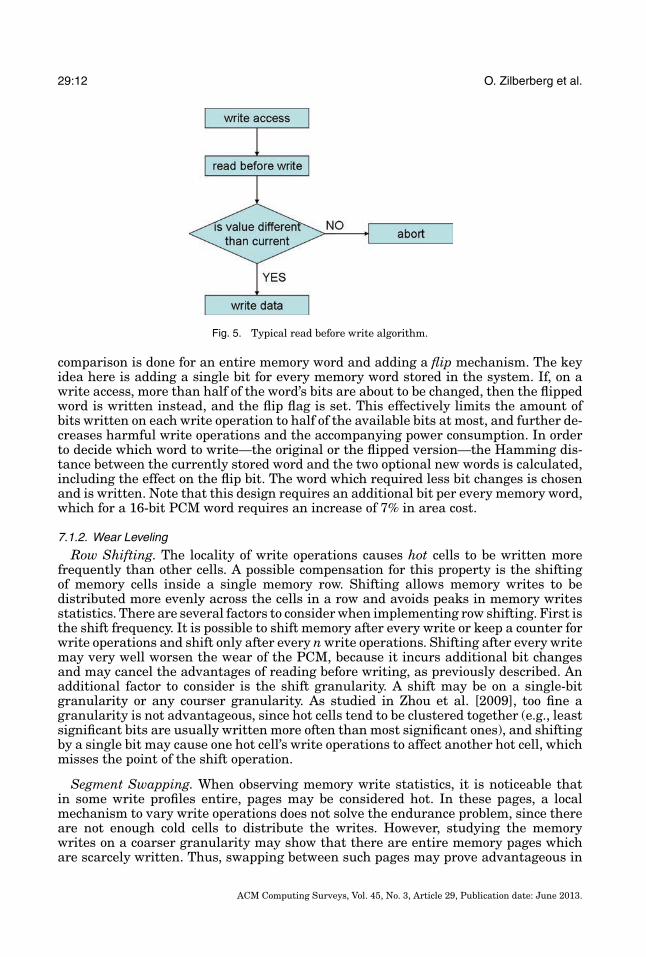
7.1.1. Bit-Level Read Before Write
PCM Design Opportunities. In conventional DRAM and flash, each write operationupdates an entire page or block, and write operations on a bit granularity level areunavailable. Furthermore, the read and write latencies for DRAM memory accessoperations are similar. PCM exhibits different attributes. Depending on the devicemanufacturer, it may be bit-accessible (though it is sometimes addressable on a page-level granularity, to emulate NOR flash [NumonyxOmneo 2010]), and its read latencyis far smaller than its write latency. These characteristics provide an opportunity fornew design schemes focused on reducing PCM power consumption and increasing itslifetime [Cho and Lee 2009; Yang et al. 2007; Zhou et al. 2009].
Redundant Writes. A DRAM or flash write operation affects an entire page or block.Owing to the value locality property, this means that individual bits are often rewrittenwith the same value stored in them. While this is of little importance in DRAM, it pro-vides an opportunity for increasing PCM lifetime, by removing these redundant writeson a bit-level. Since read operations in PCM are much faster than write operations, itis relatively cheap to precede each write operation with a read operation, as depicted inFigure 5. It is thus possible to write a cell only when its value actually changes, insteadof on any write request. The removal of these redundant write operations on a bit-levelmay increase PCM lifetime by a factor of 4.5 [Zhou et al. 2009]. It should be notedthat this method is new to PCM and is inappropriate for DRAM, because unlike PCM,the time required for a read operation in DRAM is roughly the same as for a writeoperation, rendering the read-before-write technique costly in terms of performance.This basic and simple reduction in memory write operations is common to many de-signs and can be found under several names, including Read-Before-Write [Zhou et al.2009], Flip-N-Write [Cho and Lee 2009], and Data-Comparison-Write Scheme [Yanget al. 2007].
Flip-N-Write. It has been shown how to improve upon memory write energy, band-width, and endurance by inspecting the currently written bit value and comparingit with the new required value. These parameters can be further improved if the
ACM Computing Surveys, Vol. 45, No. 3, Article 29, Publication date: June 2013.
29:12 O. Zilberberg et al.
Fig. 5. Typical read before write algorithm.
comparison is done for an entire memory word and adding a flip mechanism. The keyidea here is adding a single bit for every memory word stored in the system. If, on awrite access, more than half of the word’s bits are about to be changed, then the flippedword is written instead, and the flip flag is set. This effectively limits the amount ofbits written on each write operation to half of the available bits at most, and further de-creases harmful write operations and the accompanying power consumption. In orderto decide which word to write—the original or the flipped version—the Hamming dis-tance between the currently stored word and the two optional new words is calculated,including the effect on the flip bit. The word which required less bit changes is chosenand is written. Note that this design requires an additional bit per every memory word,which for a 16-bit PCM word requires an increase of 7% in area cost.
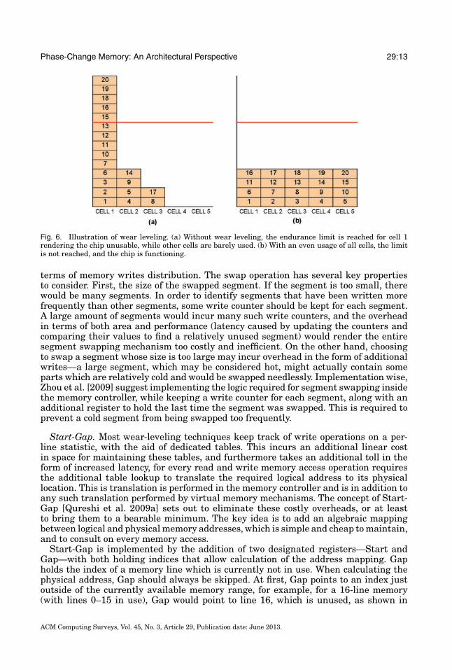
7.1.2. Wear Leveling
Row Shifting. The locality of write operations causes hot cells to be written morefrequently than other cells. A possible compensation for this property is the shiftingof memory cells inside a single memory row. Shifting allows memory writes to bedistributed more evenly across the cells in a row and avoids peaks in memory writesstatistics. There are several factors to consider when implementing row shifting. First isthe shift frequency. It is possible to shift memory after every write or keep a counter forwrite operations and shift only after every n write operations. Shifting after every writemay very well worsen the wear of the PCM, because it incurs additional bit changesand may cancel the advantages of reading before writing, as previously described. Anadditional factor to consider is the shift granularity. A shift may be on a single-bitgranularity or any courser granularity. As studied in Zhou et al. [2009], too fine agranularity is not advantageous, since hot cells tend to be clustered together (e.g., leastsignificant bits are usually written more often than most significant ones), and shiftingby a single bit may cause one hot cell’s write operations to affect another hot cell, whichmisses the point of the shift operation.
Segment Swapping. When observing memory write statistics, it is noticeable thatin some write profiles entire, pages may be considered hot. In these pages, a localmechanism to vary write operations does not solve the endurance problem, since thereare not enough cold cells to distribute the writes. However, studying the memorywrites on a coarser granularity may show that there are entire memory pages whichare scarcely written. Thus, swapping between such pages may prove advantageous in
ACM Computing Surveys, Vol. 45, No. 3, Article 29, Publication date: June 2013.
Phase-Change Memory: An Architectural Perspective 29:13
Fig. 6. Illustration of wear leveling. (a) Without wear leveling, the endurance limit is reached for cell 1rendering the chip unusable, while other cells are barely used. (b) With an even usage of all cells, the limitis not reached, and the chip is functioning.
terms of memory writes distribution. The swap operation has several key propertiesto consider. First, the size of the swapped segment. If the segment is too small, therewould be many segments. In order to identify segments that have been written morefrequently than other segments, some write counter should be kept for each segment.A large amount of segments would incur many such write counters, and the overheadin terms of both area and performance (latency caused by updating the counters andcomparing their values to find a relatively unused segment) would render the entiresegment swapping mechanism too costly and inefficient. On the other hand, choosingto swap a segment whose size is too large may incur overhead in the form of additionalwrites—a large segment, which may be considered hot, might actually contain someparts which are relatively cold and would be swapped needlessly. Implementation wise,Zhou et al. [2009] suggest implementing the logic required for segment swapping insidethe memory controller, while keeping a write counter for each segment, along with anadditional register to hold the last time the segment was swapped. This is required toprevent a cold segment from being swapped too frequently.
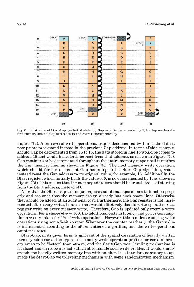
Start-Gap. Most wear-leveling techniques keep track of write operations on a per-line statistic, with the aid of dedicated tables. This incurs an additional linear costin space for maintaining these tables, and furthermore takes an additional toll in theform of increased latency, for every read and write memory access operation requiresthe additional table lookup to translate the required logical address to its physicallocation. This is translation is performed in the memory controller and is in addition toany such translation performed by virtual memory mechanisms. The concept of Start-Gap [Qureshi et al. 2009a] sets out to eliminate these costly overheads, or at leastto bring them to a bearable minimum. The key idea is to add an algebraic mappingbetween logical and physical memory addresses, which is simple and cheap to maintain,and to consult on every memory access.
Start-Gap is implemented by the addition of two designated registers—Start andGap—with both holding indices that allow calculation of the address mapping. Gapholds the index of a memory line which is currently not in use. When calculating thephysical address, Gap should always be skipped. At first, Gap points to an index justoutside of the currently available memory range, for example, for a 16-line memory(with lines 0–15 in use), Gap would point to line 16, which is unused, as shown in
ACM Computing Surveys, Vol. 45, No. 3, Article 29, Publication date: June 2013.
29:14 O. Zilberberg et al.
Fig. 7. Illustration of Start-Gap. (a) Initial state; (b) Gap index is decremented by 1; (c) Gap reaches thefirst memory line; (d) Gap is reset to 16 and Start is incremented by 1.
Figure 7(a). After several write operations, Gap is decremented by 1, and the data itnow points to is stored instead in the previous Gap address. In terms of this example,should Gap be decremented from 16 to 15, the data stored in line 15 would be copied toaddress 16 and would henceforth be read from that address, as shown in Figure 7(b).Gap continues to be decremented throughout the entire memory range until it reachesthe first memory line, as shown in Figure 7(c). The next memory write operation,which should further decrement Gap according to the Start-Gap algorithm, wouldinstead reset the Gap address to its original value, for example, 16. Additionally, theStart register, which initially holds the value of 0, is now incremented by 1, as shown inFigure 7(d). This means that the memory addresses should be translated as if startingfrom the Start address, instead of 0.
Note that the Start-Gap technique requires additional spare lines to function prop-erly and assumes that the memory design already has such spare lines. Otherwisethey should be added, at an additional cost. Furthermore, the Gap register is not incre-mented after every write, because that would effectively double write operation (i.e.,register write on every memory write). Therefore, Gap is updated only every φ writeoperations. For a choice of φ = 100, the additional costs in latency and power consump-tion are only taken for 1% of write operations. However, this requires counting writeoperations using some 7-bit counter. Whenever the counter reaches φ, the Gap valueis incremented according to the aforementioned algorithm, and the write-operationscounter is reset.
Start-Gap, in its given form, is ignorant of the spatial correlation of heavily writtenmemory addresses. It is typical in memory write operation profiles for certain mem-ory areas to be “hotter” than others, and the Start-Gap wear-leveling mechanism islocalized and on its own is not sufficient to handle such write profiles. It would simplyswitch one heavily written memory line with another. It is therefore necessary to up-grade the Start-Gap wear-leveling mechanism with some randomization mechanism.
ACM Computing Surveys, Vol. 45, No. 3, Article 29, Publication date: June 2013.

Phase-Change Memory: An Architectural Perspective 29:15
Fig. 8. (a) First-come-first-serve scheduling; (b) write cancellation; (c) write pausing.
The enhanced version of Start-Gap defines some randomization algorithm, using ei-ther a Feistel-Network based randomization, which is common in ciphers (DES), ora random invertible matrix (RIB). Either of these elements allows a pseudorandommemory of logical addresses to some intermediate address, with the added value thattwo subsequent logical memory addresses, whose write usage operations have greatcorrelation, are now mapped to different unrelated addresses. So in effect, two nearbyintermediate addresses are far less likely to have similar memory write profiles, thusremoving the locality effect. After such a randomized translation is applied, Start-Gapcan be used to level the wear of any locally hot memory line, with less likelihood thatreducing wear of one critical line would increase the wear of another critical one.
Start-Gap also provides a potential solution for the possibility of an adversary attack-ing the memory system. Should a malicious adversary be knowledgeable in the internaldesign of the memory system, including the Start-Gap technique and its parameters,it would be possible for that adversary to bring the PCM to device failure in severalseconds, due to continuous write operations to the same memory line. If, however,Start-Gap is separated to different regions of the memory system and Start-Gap reg-isters are duplicated for each such region separately, then it is possible to ensure thatthe Gap would move the assaulted line before it reaches its memory write operationslimit. The required overhead is still far less than that of other wear-level mechanisms,though it now depends linearly on the memory size and is no longer constant.
7.1.3. Write Cancellation and Write Pausing. PCM memory accesses, as opposed to DRAMmemory accesses, typically have a much higher write latency than read latency. Addi-tionally, once a write operation has begun for some memory bank, a subsequent readaccess request for the same bank must be delayed until the write request has been ser-viced, as can be seen in Figure 8(a). The increase in read requests’ latency because ofdominant write requests is 2.3x. In order to reduce the overall latency of read requests,which is performance critical in the system, it is possible to cancel or pause a writerequest even as it is being serviced [Qureshi et al. 2010a].
Write Cancellation. The key element of this design scheme is allowing the PCM cellsthe ability to cancel an ongoing write operation when a dedicated signal is sent. Thus,
ACM Computing Surveys, Vol. 45, No. 3, Article 29, Publication date: June 2013.

29:16 O. Zilberberg et al.
whenever a read request arrives for a bank which is currently being written to, the writeoperation is canceled and the read request is serviced, as can be seen in Figure 8(b).While such a cancellation may lead to inconsistency in the memory contents, as long asthe desired written values are kept in the write queue and subsequent read requestsare serviced from the write queue, the memory is coherent. To prevent an overflow ofthe write queue buffer, another mechanism monitors the queue’s occupancy, and shouldit reach some near-limit threshold, its write operations would be performed regardlessof subsequent read requests to the same bank (i.e., the write cancellation policy iswithheld). Further improvement of this mechanism arises from monitoring each writerequest to keep track of how long it has been in operation. With this statistic it ispossible to prevent the cancellation of write requests which are nearing completion,for example, a write request which is 90% complete should not be canceled. Furtherimprovement to the mechanism could be achieved by an adaptive write cancellationscheme, which sets the cancellation threshold dynamically according to the numberof entries in the write queue buffer. This way writes are forced (i.e., there is no writecancellation) if the queue is nearly full, but more writes are cancelled if the queue isrelatively empty. The threshold-based designs reduce the number of writes cancelled,and thus the number of write operations which are redone, effectively decreasing theenergy overhead of the write cancellation mechanism.
Write Pausing. Due to the iterative writes property of the PCM cell, its write proce-dure can be suspended and resumed. As seen in Figure 3, this allows a logical separationof the write operation to several distinct operations, which can be paused inbetween.This property is most beneficial for improving the read latency in PCM cells, becausewhenever a read request arrives for a memory bank which is now serving a write re-quest, the write request can be paused, allowing the read operation to be serviced, afterwhich the write operation can be resumed until completion without ever canceling thewrite process, as seen in Figure 8(c). Thus the time and energy already spent on thewrite operation need not be lost. In order to implement this policy, the iterative writesalgorithm is edited to allow the insertion of a new stage. Before the newly calculatedprogramming pulse is applied to the PCM cell, there is an additional check whethera read request is pending. If there is such a request, it is serviced before the pulse isapplied. A final optimization for this technique could be achieved by combining it withwrite cancellation. Because write operation cannot be stopped at any time, but only inbetween iterative writes, an intra-iteration write cancellation scheme can be appliedto cancel a write iteration (and not the whole write request) to allow servicing of readrequests, if the read request arrives when there is no near option for pausing the writeiteration.
7.1.4. Error Recovery, Encryption Schemes, and ECC. The limited write endurance of PCMcan often lead to faulty memory cells. Even if mitigated with wear-leveling techniques,such as described in Section 7.1.2, it is likely that at some point one or more cellswould become faulty, seemingly rendering the entire PCM chip unusable. The followingsection offers architectural techniques for contending with this scenario and effectivelyincreasing PCM lifetime.
Dynamically Replicated Memory. Assuming that it is possible to identify faulty PCMcells in a memory page, such errors can be recovered from by adding another layerof indirection and pairing two real PCM pages to appear as one physical page forall purposes. Dynamically Replicated Memory [Ipek et al. 2010] does this by adding aglobal physical to real memory page translation table, which is stored in the PCM itself.Thus, every memory access to a physical page is directed to either of two real memorypages. Two pages are paired in the table if they are found to be compatible, that is, there
ACM Computing Surveys, Vol. 45, No. 3, Article 29, Publication date: June 2013.

Phase-Change Memory: An Architectural Perspective 29:17
is no single byte which is faulty in both of them. Since PCM is nonvolatile, this newmemory translation table must also be kept on it, as it too must not be volatile. Sincethis method cannot ensure zero faults in the memory translation table itself, the tableis stored in triplicate copies on the PCM. Faulty pages and the pairing of two real pagesinto a single physical page are handled by the OS. Finally, in order for this scheme tobe feasible, the memory controller must be able to identify faulty bytes in a PCM page.This is achieved by a standard parity bit mechanism, which is common in DRAM,and assisted by an additional read operation after every write, which ensures thateither the write operation was successful or that the parity mechanism noted the error.Should the controller note that the parity mechanism is oblivious to the byte error,another single bit would be intentionally inverted, prodding the parity mechanism intorecognizing the error.
The Effect of Encryption on Wear-Leveling. In computer systems where privacy andsecurity are demanded, it is common to use some encryption scheme on the main mem-ory to protect its contents from being extracted and used maliciously [Kong and Zhou2010; Seong et al. 2010a; Seznec 2010]. While this may help to increase the system’sprivacy, in some cases it has the side effect of seriously reducing the effectiveness ofwear-leveling schemes. The basic problem of encryption in this context is its changingof the data stored in the memory. Encryption often works on block sizes, which aresmaller then the block sizes of the cache level. Additionally, a key principle of most en-cryption schemes is the principle of diffusion, which dictates that a change to a singlebit in the block affect the entire block, or at least most of it. This is completely orthog-onal to the assumptions on which wear-leveling schemes below cache-line granularityare based. Such schemes, such as the removal of redundant bytes on a bit-level, areprimarily based on the statistical properties of write operations which state that inmost blocks written to the memory, an abundant amount of bits remain unchanged bythe write operation. This assumption is naturally invalidated by the introduction of anencryption scheme, as even a change in a single bit may toggle a change in most of thebits of the encrypted block. Encryption also disables the partial writes scheme, sincethe entire cache line is changed and needs to be rewritten even if only a single word isdirty.
Block-Level Counters. In order to mitigate the negative effect of encryption schemeson the wear-leveling techniques described, it has been suggested to provide the en-cryption scheme with additional counters on a block level, on top of the single counteron a cache-line level. In this way, when a write-back occurs, only the counters of thewritten-back block are updated, and there is no need to rewrite the entire cache, excepton the rare event that the block-level counter overflows, in which case the cache-linelevel counter is incremented and the entire cache-line is re-encrypted and rewritten tomemory.
ECC Increases Lifetime. When considering the limited lifetime on the PCM, even ifsome architectural designs are adopted to lengthen it, the question of what to do withthe device when it finally does fail still needs to be answered. In order to continue usingthe system in a stable and reliable manner, it is possible to introduce error-correctioncodes (ECCs) to mitigate PCM device failures by correcting bit errors in memory readdata. Ideally, if enough space is allocated in favor of the ECC algorithm, it can makethe PCM robust to bit failures. However, increased space obviously increases cost andreduces PCM effectiveness. Additionally, during PCM’s initial lifetime, it has only afew bit errors at most, and space allocated in favor of ECC is wasted.
It would therefore seem advantageous to apply some adaptive ECC scheme tothe PCM which takes into account the amount of write operations to the PCM, or
ACM Computing Surveys, Vol. 45, No. 3, Article 29, Publication date: June 2013.

29:18 O. Zilberberg et al.
specifically to any of its lines, and utilizes a sufficiently strong ECC to fix any expectedbit errors. This can be done by dividing the memory addresses into several groups, witheach group allocating some of its memory pages in favor of ECC. Each group also keepssome statistics on the write operations to it which are kept in the form of a counter,and when this counter reaches some predetermined factor, it causes an interrupt to theOS, which is aware of the adaptive ECC scheme and can reorganize the group so as toallocate more space for the ECC, until after some final threshold, the entire group ismarked as faulty and no memory is ever allocated from it by the OS. It is claimed thatusing the PCM itself to store the ECC is beneficial because it saves the need for extrahardware and also because it is quite unlikely for the ECC pages themselves to reachthe write limit threshold that is defined in this scheme.
Encryption and ECC Combined. As discussed, use of adaptive ECC requires countersto keep track of write operations. This can be done either by keeping a counter for eachcache line, which is costly in terms of space, or by keeping a single counter for the entirepage, which requires very little space but is far less accurate since writes to differentlines in the same page are accumulated, instead of being considered a single write.
In order to improve the accuracy of this statistic without having to store additionalcounters on a cache-line level, the aforementioned encryption scheme can be utilized.Each cache line already has some counter for encryption purposes, which is updatedby write operations to that line and in effect counts write accesses to that line. Withthe addition of some global counter on a page-level granularity, ECC can keep track ofwrite accesses to each page with nearly no additional hardware cost other than costsalready incurred by the encryption scheme.
Error-Correction Pointers (ECP). The usage of error-correction codes (ECC) is com-monly employed to correct errors in DRAM-based memories, and has also been sug-gested for PCM. However, it should be noted that DRAM and PCM memories exhibitdifferent behaviors regarding errors. The charge-based DRAM is commonly affected bysoft errors, that is, leakage-related errors in a write operation, which affect only theresults of that particular write operation and are reset on the next write operation.PCM, however, is prone to hard errors, that is, specific memory cells can fail completelywhen written too many times. It would therefore be more efficient to mark these cellsas unusable and replace them with other functioning cells, rather than attemptingto correct the error using ECC, especially since ECC requires additional writes andmay be contradictory to other wear-leveling techniques employed. The ECP [Schechteret al. 2010] scheme stores pointers to defective memory cells and their correspondingdata. Thus, whenever a read-write-read operation fails, a pointer is stored to the faultycell with the required written data, and upon read operation, the correction pointer isconsidered prior to the actual data stored in the PCM cell. This scheme can also beused to mitigate errors in the pointers themselves.
Stuck-At-Fault Error Recovery (SAFER). A data block which contains faulty bits (i.e.,bits stuck at a certain value) can be partitioned into several sub-blocks, where eachsuch sub-block has at most one faulty bit [Seong et al. 2010b]. In this manner, it ispossible to employ a simple technique to recover from a single-bit error on such sub-blocks, avoiding rendering the entire block or page unusable. The trick to overcominga single fault is to keep a single inversion bit for every such sub-block. On every writeoperation, the faulty bit is checked. If it holds the required value (there is generally a50% chance of that occuring), the sub-block can be read later without error. Otherwise,if the faulty bit holds the inverted value of the written bit, the entire sub-block can beinverted and the inversion bit set. Subsequently, a read operation would recognize thatthe sub-block is inverted and invert back the read data. In order to prevent duplicate
ACM Computing Surveys, Vol. 45, No. 3, Article 29, Publication date: June 2013.

Phase-Change Memory: An Architectural Perspective 29:19
write operations on every faulty sub-block, a dedicated cache can hold addresses offaulty bits and their stuck-at values, so that the value of the inversion bit and thewritten data could be determined before the actual write operation.
Fine-Grained Remapping with ECC and Embedded Pointers (FREE-p). Previoustechniques have employed some dedicated memory storage area in order to eitherstore some backup for faulty memory bytes or simply to keep track of the addresses ofthese bytes. FREE-p [Yoon et al. 2011] offers to use the faulty memory block itself inorder to embed a pointer to the replacement memory block. In this manner, a faulty64B block can hold a 64b address pointer to its replacement. Because of the high spaceredundancy used for the pointer, it is possible to use a powerful ECC to ensure correctencoding and decoding of the pointer, such as a 7-modular-redundancy (7MR) ECCwhich repeats the 64b address 7 times in the allocated 64B block. An additional bitis reserved for each 64B block to mark it as faulty. When a read operation occurs,the faulty bit is read first to determine whether the actual data should be read or anindirection followed. If errors are detected in the block pointed to, multiple indirectionpointers could be used in a linked-list fashion, with an additional mechanism thatupdates the first pointer to point at the last segment in the chained loop, for addedefficiency of read operations. If a 64B block becomes too faulty to store even the small64b address, the entire page is rendered unusable and replaced, as in previously de-scribed schemes. An advantage of FREE-p over other error recovery schemes rests inits ability to recover from many local errors, such as a single cache-line failure.
7.1.5. Buffer Organization and Partial Writes. In using PCM as an alternative to DRAMmain memory, it is beneficial to consider the memory array architectural organization.A PCM cell, very much like DRAM, is organized into different banks, blocks, and sub-blocks. These blocks share among them the peripheral circuitry required to operatethe memory array, most notably the sense amplifiers and write drivers. These largedevices take a heavy toll on PCM [Lee et al. 2009], and an efficient buffer organizationshould be adopted to reduce usage of these devices.
In this typical memory architecture, reading a row from the memory requires latchingit to a memory buffer, from whence it is read and to which it is written. Any read or writeaccess to an unbuffered row requires that the buffer would be evicted in order to makeroom for the next accessed row. In DRAM memory, every such row eviction requires thatthe data evicted from the row be rewritten to memory, owing to DRAM’s destructiveread operations. In a PCM-based architecture, however, it is seldom required that thedata be rewritten, except when it has changed.
In order to compete with DRAM’s superior energy write costs and access latencieswhile maintaining the same area costs, the described architecture should be altered.Using the same space occupied by the buffered row, along with its accompanying senseamplifiers, it is possible to maintain narrower buffers with multiple buffer rows. Theamount of sense amplifiers required to operate the buffer is linearly dependent onthe buffer width, hence the great cost reduction when narrowing the buffer. This costreduction can be utilized to support several buffer rows with full associativity betweenthem, which reduces the amount of memory write operations due to buffer eviction,greatly increasing average PCM access performance.
Narrower buffers reduce the PCM energy writes and help bring it to the same levelas that of DRAM, but at a performance cost—a narrow buffer has poorer utiliza-tion of memory accesses spatial locality and provides fewer opportunities for memorywrite accesses coalescing. Mitigating these performance costs with a fully associative,multiple-row design with the same area cost as the original architecture can decreasePCM delay penalties, when compared with DRAM design, from 1.60x to 1.16x, and alsodecrease memory energy costs from 2.2x to 1.0x [Lee et al. 2009].
ACM Computing Surveys, Vol. 45, No. 3, Article 29, Publication date: June 2013.

29:20 O. Zilberberg et al.
This design can be further developed to account for the limited PCM write endurancein the form of partial writes. This technique keeps track of the dirty data through allcache levels up until they are written to the memory banks. In this manner, evicteddata from any cache level is only written to the main PCM memory if it has changed,reducing the amount of unnecessary write operations. This scheme is considered ontwo granularities. Lowest-level cache bitline size (64B) and word size (4B). It is notconsidered on a per-bit granularity, since this incurs too great an overhead in storedmetadata or otherwise requires the use of comparators. Keeping track of memorywrites on the suggested granularities is possible by keeping track of memory writeinstructions from the microprocessor pipeline. Using partial writes on a lowest-levelcache bitline size requires a 0.2 percent increase in memory usage, while utilizing iton a word-size granularity has an increased 3.1 percent overhead [Lee et al. 2009].
7.1.6. Morphable Memory System. As described in Section 4.2, PCM cells can be eithersingle-level (SLC) or multilevel (MLC). While MLCs provide higher density, the itera-tive algorithms required to accurately read and write data to these cells take a toll onthe device latency. Depending on the load services, some systems may benefit from theuse of MLCs with their higher density, while some workloads which are not capacity-intensive may result in degraded performance due to usage of MLCs. The purpose ofthe Morphable Memory System (MMS) is to benefit from both designs by incorporatingboth of them into the system, while dynamically setting the portion of PCM cells usedas MLCs to account for varying workloads [Qureshi et al. 2010b].
In MMS, the memory pages are kept in either of two states. The high-density PCM(HDPCM) are pages in which the PCM cells are treated as MLCs, and the low-densitylow-latency PCM (LLPCM) are pages in which PCM is treated as SLC for reducedlatency. Using a memory monitoring circuit, the MMS architecture is able to determinethe portion of memory to be treated as HDPCM according to the capacity required bythe varying workload. In order to correctly translate logical addresses to physicaladdresses and also provide current memory page allocations, the MMS collaborateswith the OS which must be aware of pages in the LLPCM section of the memory, asthese provide less memory capacity than is otherwise assumed by the software, whichnormally treats all memory addresses as belonging to HDPCM, thus providing greatercapacity.
In order to estimate the memory capacity requirements of the system, a specializedmemory monitoring circuit (MMON) is designed. This circuit estimates memory usagestatistics using stack distance histogram analysis. The results of the MMON statisti-cal algorithms are periodically read by the OS to determine subsequent handling ofmemory page allocations. Whenever the OS is informed of a lack of LLPCM pages,it evicts some HDPCM pages, enabling them to be used as LLPCM. Alternatively,LLPCM pages may be converted to HDPCM pages when they are evicted by cachingwrite mechanisms or when the MMON detects that workload capacity requirementsare on the rise, requiring increased PCM density.
7.1.7. Software Opportunities. Using PCM (or any other nonvolatile memory technology)in place of DRAM as main memory offers several conceptual advantages for softwaresystems utilizing the nonvolatile property of the memory. While this is somewhatbeyond the scope of PCM architecture, it does provide an extensive research field.Some recent key works are presented here.
Byte-Addressable Persistent File System (BPFS). Traditional file systems are de-signed for best performance with traditional block-accessed memory technologies.BPFS offers performance enhancements by utilizing byte-accessible nonvolatile mem-ory technologies, such as PCM [Condit et al. 2009]. BPFS requires use of atomic write
ACM Computing Surveys, Vol. 45, No. 3, Article 29, Publication date: June 2013.

Phase-Change Memory: An Architectural Perspective 29:21
operations and write ordering mechanisms implemented in hardware. Using these ca-pabilities, it allows for storing of simple data structures in persistent memory, whilestoring complex data structures in volatile memory. In order to ensure reliability, BPFSuses short-circuit shadow paging (SCSP). While most file systems use either logging orshadow paging (with shadow paging generally being less efficient), BPFS implementsSCSP which allows for efficient commit operations to any location in the file systemtree, due to memory byte-addressability and fast random write. The main drawbackof BPFS resides in its need of dedicated hardware support and its nonstandard filesystem, which may require extensive adaptations of traditional computerized systems.
Nonvolatile Memory Heaps (NV-heaps). Architecting software for byte-addressable,nonvolatile memory systems has several advantages over traditional systems, but mayalso lead to some dangerous pitfalls. NV-heaps [Coburn et al. 2011] provide program-mers with several primitives to ease work with nonvolatile memory while protectingthem from common bugs. These primitives include objects, pointers, memory alloca-tions, and atomic sections. They ensure pointer safety (e.g., protection against pointersin nonvolatile memory which point at locations in volatile memory), ACID transactions,traditional API (similar to volatile-memory based data structures), high performance,and scalability. Finally, NV-heaps provide the application with direct access to thenonvolatile memory, skipping operating system overheads.
Mnemosyne. The Mnemosyne architecture [Volos et al. 2011] provides programmerswith an interface for direct access to nonvolatile memory, without any hardware con-straints on PCM device design. Global data that should be stored in nonvolatile (per-sistent) memory is declared by programmers using the dedicated pstatic keyword. Thisdirect nonvolatile memory access not only removes the need for data serialization intofiles in block-based file systems, but also does not require any special adaptation of thefile system. Mnemosyne does not offers an alternative file system, but instead offer afast mechanism for storing simple data which should be kept persistent. By provid-ing user-mode access to persistent memory and offering the programmer mechanismsfor consistent updates to the persistent memory, all the while requiring no hardwarechanges, Mnemosyne appears to be a feasible, simple-to-implement architecture, whichis decoupled from PCM hardware architecural considerations.
7.2. Hybrid PCM and DRAM Memory
In most conservative main memory designs, the main memory homogeneously consistsof a single type of memory, for example, DRAM or PCM. In order to overcome thechallenges of implementing main memory using PCM while still making use of theadvantages of DRAM, a hybrid design which consists of PCM-based main memorywhile using a small DRAM buffer is considered [Dhiman et al. 2009; Qureshi et al.2009b; Ramos et al. 2011]. This allows for utilizing DRAM’s superiority in terms of bothlatency and endurance to avoid those disadvantages in the PCM, while still buildingthe majority of the main memory with PCM, with its superior density and scalability.This design is depicted in Figure 4(c). We also note that such hybrid designs may alsobenefit 3D die-stacking designs [Zhang and Li 2009], though these aspects are beyondthe scope of this article.
Organization. Using PCM as the computer system’s main memory is identical in itsorganization to traditional DRAM usage as main memory, with an operating-systemaware page table. The addition in the hybrid main memory organization is a smallDRAM buffer of which the OS is not aware [Dhiman et al. 2009; Qureshi et al. 2009b;Ramos et al. 2011]. As seen in Figure 9, it is managed internally in hardware by themain memory controller, similar to memory caches.
ACM Computing Surveys, Vol. 45, No. 3, Article 29, Publication date: June 2013.

29:22 O. Zilberberg et al.
Fig. 9. A hybrid PCM and DRAM memory design with memory controller and write count statistics table.
Lazy-Write. The Lazy-Write organization technique [Qureshi et al. 2009b] uses theDRAM buffer to take advantage of the low latency of DRAM, compensating for the PCMmain memory’s inferior access and write speeds. Furthermore, it reduces the amountof actual write operations to the PCM memory, thus improving its limited lifetime.
The concept of this organization is that when a page fault occurs and a page must bebrought into the main memory from the HDD, it is first inserted into the fast DRAMbuffer instead of the slower PCM main memory. A page is allocated in both DRAMbuffer and PCM memory, but the data is copied only to the buffer. Hence, read timefrom the HDD incurs relatively short DRAM latency instead of the longer PCM latency.Additionally, the memory controller holds two state bits for each page in the DRAMbuffer—present and dirty. Pages which are marked with the present bit in the DRAMbuffer are also present in the PCM main memory. This of course means that upon pagefault, the page that is brought into the DRAM buffer has its present bit set to 0. Whena page is replaced in the DRAM buffer, if it is dirty, it is written to the PCM memoryfirst, to maintain consistency. This technique reduces redundant write operations tothe endurance-wise limited PCM memory.
In addition to the DRAM buffer, a fast PCM write queue is used when actuallywriting to the PCM memory. This write queue, which is much faster than the PCMmain memory, amortized the time spent for write operations. The DRAM buffer doesnot write directly to the PCM memory, and thus does not have to wait for the PCM’slong latency. On the other hand, The write queue is large enough so that it does notget filled, and the written pages are transferred from it directly into the PCM, whichincurs the long PCM latency cost, but since only the write queue is affected, the systemas a whole is oblivious to this latency.
In short, the application of these two memory devices—the DRAM write buffer andthe PCM write queue—in addition to the PCM main memory, helps reduce write oper-ations to the PCM and compensate for its relatively high latency.
Line-Level Writes. It has already been suggested [Qureshi et al. 2009b] that theDRAM write buffer be used to write to the PCM main memory only pages which havebeen marked as dirty, that is, pages which have been written over since their lastread from the main memory or HDD. In order to further improve upon this technique,the writing of the dirty pages into the PCM memory has to be considered on a finergranularity. This is done by considering chunks smaller than a whole memory pagewhen deciding whether a certain datum is dirty and must be written back to the
ACM Computing Surveys, Vol. 45, No. 3, Article 29, Publication date: June 2013.

Phase-Change Memory: An Architectural Perspective 29:23
memory. The proposed granularity for consideration is the size of a cache line. Thisallows for only chunks which have been changed in the cache, and thus differ fromtheir original values as stored in the main memory, to be written back. It incurs thegreater cost of keeping track of each chunk’s dirty state, instead of a unified dirty bit forthe entire page, but can save a significant amount of redundant write-back operationswhich reduce PCM lifetime.
Fine-Grained Wear-Leveling in the Hybrid Architecture. Several techniques havebeen discussed here in order to reduce PCM wear in the DRAM and PCM hybridmemory organization [Dhiman et al. 2009; Qureshi et al. 2009b; Ramos et al. 2011].While these techniques indeed decrease PCM write operations and help achieve thegoal of increasing its lifetime, they are not complete without some wear-leveling mech-anism. The granularity of the proposed wear-leveling mechanism is imposed by theline-level writes mechanism previously described. Analyzing memory write accessesinside a single page shows that the distribution of memory writes on a cache-line gran-ularity inside a single page are nonuniform, and some cache lines are written moreoften than others. This nonuniform wear obviously reduces the memory’s lifetime. Tak-ing this uneven distribution into consideration, the idea here is to apply a cyclic shifton a cache-line scale, so that while some cache lines are logically written to more oftenthan others, physically the wear is evened out over all cache lines in a page.
Like most wear-leveling mechanisms, it is imperative to hold some translation oflogical addresses to physical addresses. In this proposed fine-grained wear-levelingmechanism, some register holds the size of the cyclic shift per memory page. Forexample, a 16-line memory page incurs a 4-bit register to hold its shifting value. Somerandom number generator is used to supply an initial value for the cyclic shift when thepage is replaced. In this manner, each time the page is replaced, its shift register holdsa varying evenly-distributed number, thus leveling the write wear across all cache linesin the page.
Page-Level Bypass. Memory usage profiling of various applications shows that someapplications have poor memory reuse [Qureshi et al. 2009b]. An example of such appli-cations is one which relies on streaming data. Such data are read once, used, and arethen rendered irrelevant by the arrival of new data. As described earlier, memory pagesread from the HDD are first stored in the DRAM buffer. When these pages are replacedby the new data, they are stored in the PCM. But the profiling shows that these pagesare no longer needed by the application, and hence writing them to the PCM is notbeneficial performance wise and only serves to wear the PCM cells, reducing its overalllifetime.
For such applications, it would prove beneficial to mark them for bypassing thePCM. Such a page-level bypass (PLB) flag would serve to dispose of memory pagesreplaced in the DRAM instead of writing them back to the PCM, saving redundantwrite operations. Such memory profiling is not done by the hardware itself—it can onlybe predefined, and the PLB set by the operating system.
Memory Controller and Page Manager. Hybrid PCM and DRAM architectures canalso benefit from an OS memory handling policy, which is aware of the hybrid memoryarchitecture [Dhiman et al. 2009]. Such a design incorporates architectural changes inboth the memory controller (hardware) and the page manager (OS—software).
The memory controller routes memory access requests to the relevant hardwareaccording to the requested address, whether it be in the DRAM section of the memory,or the PCM. It also keeps track of all PCM accesses on a page-level granularity (seeFigure 9). This allows the controller, which is aware of PCM’s limited endurance, tomark a PCM page as a “bad” page, once it has reached its theoretical limit for write
ACM Computing Surveys, Vol. 45, No. 3, Article 29, Publication date: June 2013.

29:24 O. Zilberberg et al.
accesses. This should prevent any future page allocations from reaching this hot page,while the rest of the PCM is still usable. Additionally, once the amount of memory writesto a single PCM page has reached some predetermined threshold, a page swap occurs,which is handled by the page manager and should transfer the hot virtual page to someother physical portion of the PCM, so as to provide wear leveling. These statistics, whichare maintained by the memory controller, may be kept in a small dedicated SRAM cacheso that this maintenance does not degrade PCM lifetime. Finally, since these statisticsshould be kept throughout the lifetime of the system, they are copied to the disk onshutdown and reloaded on startup, while also synchronizing the data with the diskperiodically to account for system crashes.
The page manager is the software part of this design scheme, and with it, the OSensures PCM wear leveling and an optimal use of the hybrid memory architecture.It consists of two key elements—the memory allocator and the page swapper. Thisdesign scheme assumes different behaviors for PCM page allocator and for DRAMpage allocator. DRAM design is outside the scope of this work, and thus only thePCM allocator is discussed. The PCM allocator keeps four lists of memory pages: free,used-free, threshold-free, and bad. Initially, all pages are marked as free. After anallocated page has been freed, it is marked as used-free, to indicate that it is free forreallocations but has already been used recently, while other pages have not. Wheneverthe free list is exhausted, it is merged with the used-free. Also, as discussed regardingthe memory controller, a page which has been written to more than a predeterminedthreshold amount of times is moved to the threshold-free list. This is done by the pagemanager by handling the page-swap generated by the memory controller, thus ensuringthat this page will not be written to again until all memory pages have reached thethreshold. This scheme provides an OS-based wear leveling for the PCM on a page-level granularity. The final list of bad pages contains pages which have reached theirtheoretical endurance limit and should never be used again, for fear of write or readfailures.
When swapping pages, the page manager updates all relevant memory componentsto comply with memory coherency—page table entries, TLB entries, and the pagecontents themselves. It is also possible to choose from a simplistic memory swap policy,which always allocates pages from the PCM, or a hybrid policy. The simple policy hasadvantages of its own, as it provides some wear leveling for the PCM, independentof DRAM memory, and can be beneficial. However, the hybrid policy achieves the truegoal of this design policy, as it provides a DRAM backup for the PCM endurance-limitedcells. Such a policy not only reduces memory writes to the PCM but also allows heavilywritten memory pages to be placed in the DRAM, thus reducing the amount of pageswap interrupts raised for these pages and removing a major bulk of PCM endurancecostly writes.
8. SOLID-STATE DISK DESIGNS
8.1. Background
In recent years, advancements in solid-state disk (SSD) technology and nonvolatilememories (NVM) have led to NAND flash memory being used extensively in variousapplications, such as mobile devices, hard disk caches, and even HDD replacements[Sun et al. 2010]. While NAND flash is still a preferable choice for such applications,it has some limitations which need to be addressed in any future developments andapplications of the technology.
One such shortcoming of NAND flash technology lies in the asymmetry between itsread and write operations [Kim et al. 2008; Sun et al. 2010]. A NAND flash memoryread request can access any of its pages directly. However, that is not the case for write
ACM Computing Surveys, Vol. 45, No. 3, Article 29, Publication date: June 2013.

Phase-Change Memory: An Architectural Perspective 29:25
Fig. 10. Flash memory based SSD typical architecture with the flash tranlation layer.
operations. NAND flash pages cannot be written directly. Instead, before any writeoperation, the memory area being written has to be erased first. Furthermore, NANDflash cannot be erased on a single-page granularity. Instead, a single erase unit hasto be erased. Such an erase unit typically consists of several adjacent pages, not all ofwhich should be changed by the write operation. So, in effect, in order to write a NANDflash memory page, an entire erase unit has to be backed up, erased, and subsequentlyrestored from the backup, with the updated version of the written page.
PCM has been shown to have superior endurance over NAND flash memory, but as ithas not yet been manufactured on a large scale with a cost competitive to flash memory,it provides an opportunity for hybrid architectures which benefit from the advantagesof both technologies [Boboila and Desnoyers 2010; Park et al. 2008; Yoon et al. 2008].
Flash Translation Layer. The most common solutions to the problem of erase-before-write in NAND flash memories have to do with using a flash translation layer (FTL)[Boboila and Desnoyers 2010; Park et al. 2006; Kim et al. 2008]. As seen in Figure 10,this abstraction layer translates between the file system and the physical flash pages,giving the flash device write operations the feel of regular HDD access operations. Theextra layer redirects write requests by the file system to erase-free physical pages. Thusnot all memory write requests result in immediate costly erase operations; instead,pages are written to physical memory areas which require no erase, while the originaldata page is marked as invalid. Of course, once all pages have been exhausted in thismanner and there are no longer any erase-free memory pages, entire erase units haveto be merged so that previously invalidated pages are erased, freeing up room formore write operations, while updated data from previous write operations are mergedconsistently. This method incurs a trade-off between faster write operations due to lessfrequent erase operations and the costly merge operations.
ACM Computing Surveys, Vol. 45, No. 3, Article 29, Publication date: June 2013.

29:26 O. Zilberberg et al.
Fig. 11. IPL design.
It should be noted that the FTLs are mostly implemented as firmware and areproprietary of their respective manufacturers. One should therefore keep in mind thatacademic papers regarding FTL designs, some of which are surveyed here, may notnecessarily be aware of the latest designs of industrial FTLs, as these designs are notpublicly available.
FTL Mapping Schemes. FTLs can map logical addresses to physical addresses onvarying resolutions [Park et al. 2006; Kim et al. 2008]. There are FTLs which translateon a page-level granularity, giving good performance for random access write patterns,but requiring a rather large amount of mapping information. Other FTLs map on ablock-level granularity, requiring a significantly smaller amount of mapping informa-tion, but suffering a performance degradation owing to the extra operations requiredon the entire block, even when only a part of it has been written to. Finally, the logblock mapping scheme combines both page-level mapping and block-level mapping bydividing each memory block into a data block and a log block. Block mapping is usedfor the data blocks and page mapping is used for the log blocks. Initially, every writeoperation is performed on the log block. Once it runs out of free space, the FTL mergesboth sections of the block. The size of the log block is fixed by design to avoid the largememory requirements of the page-level mapping.
8.2. PCM-Based Log Region
In-Page Logging. In-page logging (IPL) is a further improvement on the log block ad-dressing method explained in the previous section [Lee and Moon 2007; Sun et al.2010]. In IPL, instead of storing the entire updated page in the log section, the logsection is divided into several log sectors. These log sectors are used to keep track ofupdated data only, and not the entire page. They can be allocated on demand and mayalso contain more than a single update record. These records are written back to theNAND flash memory when all log pages of a single erase unit are dirty or full, butthe data page itself does not have to be written back, since all updates are stored inthe log sectors. A schematic design can be seen in Figure 11. This method gives im-proved performance over traditional log block addressing, but still suffers performancedegradation because no in-place updating can be done for the log pages, since that isstill a limitation of NAND flash memory. Furthermore, a scenario of frequent writes
ACM Computing Surveys, Vol. 45, No. 3, Article 29, Publication date: June 2013.

Phase-Change Memory: An Architectural Perspective 29:27
to a single erase unit exhausts its log sectors quickly, triggering frequent costly mergeoperations between data and log sections.
PCM-Based IPL. In order to exploit the advantages of PCM over NAND flash mem-ory, such as improved endurance and in-place updating, it is suggested to use hybridarchitecture in which PCM is used for the log region [Sun et al. 2010]. This design uti-lizes a special log region controller which is responsible for address translation betweenthe NAND flash data pages and PCM-based log pages.
A read operation accesses both memory types, where the data is first taken from theNAND flash data pages, and any further updates recorded for these pages are takenfrom the PCM log section, thus forming a complete, updated memory page. Writeoperations should first access the PCM log section. If no log records for the writtenpage exist, then a new record should be allocated. If the page already has some logrecords associated with it, their contents are compared address-wise. Records whichapply to the same memory address are overwritten (which could not have been donewith NAND flash), and if no such records exist for the specific address, then a newrecord is allocated along with the other records for the same page. A merge operationis similar to previous schemes, where the log sector updates are applied to the datapages, while writing them to a different free erase unit.
Since the log section is smaller than the data section, the latency incurred by theperipheral access devices to it is smaller than the latency to access the data pages, andsince these occur simultaneously, there is no extra latency incurred due to the usageof the hybrid memory scheme. Furthermore, PCM usage allows for in-place updating,which greatly reduces the amount of new log sectors allocated, and even though eachwrite operation requires memory address comparison to check whether a log sectoralready exists, this overhead is dwarfed by the reduction in unnecessary writes, espe-cially if keeping in mind that the PCM read operations are much cheaper than writeoperations. Finally, since PCM allows for read accesses with byte granularity, only thelog records that are relevant to the read memory page are loaded, in contrast withNAND flash which requires loading an entire page or even several pages if the logrecords stretch out over several different memory pages.
Another aspect to consider if utilizing PCM for log pages is how to allocate the logregion. Traditionally, IPL states that each erase unit has a fixed amount of log pages[Lee and Moon 2007]. This may be necessary when using the NAND flash itself for thelog region, and its main advantage is in its simple design and easy address translation.However, in such a scheme, a merge operation occurs when the fixed size of the logregion has been fully used for a given page, incurring a performance cost while otherpages on the log region have yet to be utilized. This scheme is called a static logregion assignment. In contrast, using PCM, it is possible to use the dynamic log regionassignment [Sun et al. 2010]. In this scheme, the number of log sectors assigned foreach erase unit is not fixed, but instead allocated based on the amount of updates forthat particular unit. This allows for a significantly lower amount of merge operations,since more log sectors can be allocated for a frequently updated erase unit, which isparticularly beneficial for asymmetric write profiles.
Finally, the hybrid architecture suggested improves the overall endurance of thememory, since most update operations do not affect the NAND flash, but only the PCM,which has much greater endurance. In order to optimize the endurance benefits, it isimportant to make sure PCM does not fail before the NAND flash, that is, the log regioncan be written to more often than the data region, but only by a factor determined bythe ratio of PCM endurance to NAND flash endurance. Knowing this ratio beforehand,it can be set as a threshold to the amount of updates per page stored in the log regionbefore a merge operation is forced, even if not all log pages are full. This way, the log
ACM Computing Surveys, Vol. 45, No. 3, Article 29, Publication date: June 2013.

29:28 O. Zilberberg et al.
pages and data pages wear out at the same pace. Further improvements for the logregion lifetime can be obtained by utilizing some wear-level mechanisms, as previouslyelaborated in Section 7.1.2. It should be noted that while wear-leveling schemes arecommon in flash memory designs, such designs are not necessarily applicable for PCM.Since PCM is faster than flash memory in terms of both read and write accesses, itswear-leveling designs are under more limiting constraints, and it is less desirable toimplement software-based solutions for wear-leveling. Thus PCM wear leveling designsmay be different than flash memory designs.
8.3. Metadata Separation
Metadata and User Data. File systems generally keep track of user data and metadata.Every file updated incurs both a user data update and metadata update, which inNAND flash memory are both sent to the FTL, as previously described. While thesize of metadata is usually much smaller than a file system block, it is neverthelessupdated quite frequently, in about half of memory write operations [Kim et al. 2008;Park et al. 2008]. Additionally, analyses show that only a small portion of the metadatais usually changed upon a write operation. This incurs a rather expensive cost whenwriting to NAND flash memory, especially since the metadata and user data are notusually stored together in the file system, which means that such a write operationto NAND flash would access several memory blocks, breaking the sequential writes tothe memory and increasing the amount of log records and merge operations.
FSMS and PFFS. File System Metadata Separation (FSMS) is a technique whichseparates metadata from user data [Kim et al. 2008]. The idea is to add a PCM deviceto store the metadata only. This requires a change in the block device driver to allow itto identify metadata writes according to their addresses. Once such a write has beenidentified, it is sent to a PCM filter device instead of to the NAND flash memory. Thisfilter is responsible for carrying out only necessary write operations, using a read-before-write scheme.
Alternatively, the file system metadata itself could be altered to account for thehybrid architecture. This is done in the PCM-based Flash File System (PFFS) [Parket al. 2008]. The idea here is to maintain file system metadata, such as directorystructure, in the PCM while enhancing the file system metadata to account for thespecific structure of both NAND flash and PCM.
Hiding Address Translation. Demand-based Flash Translation Layer (DFTL) [Guptaet al. 2009] is a recent FTL design which is based entirely on page-level granularityaddress translation. It relies on the assumption that most workloads have temporaladdress locality, and therefore, there is no need to store the entire page mapping tablefor easy access, but instead, a caching mechanism is employed that allows quick addresstranslation for hot pages. Non-cached address translations are stored in the flash itself,thus saving DRAM space.
Hiding address translation (HAT) is a hybrid memory architecture utilizing flash, asmall portion of DRAM, and a PCM device [Park et al. 2006]. It is an upgraded FTLbased on DFTL, but which stores the small cached address map on DRAM for quickaccess, while keeping the rest of the address translation map on a PCM device, utilizingits advantages (i.e., in-place updating, superior endurance), as previously detailed.
Chameleon. While not using PCM devices in itself, the Chameleon [Yoon et al. 2008]architecture is interesting in itself, since it is based on a hybrid of flash and FRAMtechnologies, which may also be applicable for PCM. This is another architecture whichattempts to reduce the costly random access write operations on the NAND flash, since
ACM Computing Surveys, Vol. 45, No. 3, Article 29, Publication date: June 2013.

Phase-Change Memory: An Architectural Perspective 29:29
these are the most harmful to common FTL schemes’ performance. This architectureseparates any metadata from the actual written data and stores the metadata on theFRAM instead of on the flash device. The metadata mentioned here is not a file systemgenerated metadata but, instead, the block mapping table of the FTL, pointers used bypage-level write buffers, and so forth.
8.4. Hybrid Flash Translation Layer
Hybrid Flash Translation Layer (hFTL) [Kim et al. 2008] is a page-level granularitymapping based FTL, which incorporated PCM to store mapping information, thusreducing the main memory consumption due to mapping metadata. All metadata,including the mapping table, physical page status bitmaps, and the physical blockinformation are kept on PCM, and only the data blocks are stored on the NAND flashmemory.
The NAND flash memory blocks are also divided into data blocks, buffer blocks,and garbage blocks. Newly arrived data is always stored in the buffer blocks. Once abuffer block runs out of space, it is relabeled as a data block, and a new buffer blockis allocated from the pool of garbage blocks. Should the amount of garbage blocksdecline below a predetermined threshold, a merge operation occurs. As explained, allmetadata is stored in the PCM. However, in order to account for slower PCM writeswhen compared with main memory, metadata which is related to the currently writtenbuffer block, is temporarily stored in the main memory. Only when the buffer block isrelabeled as data block is its metadata copied to the PCM.
In order to further reduce merge operations costs, hFTL implements the logical-page-delete function, which is called whenever the file system deletes a file. This functioninvalidates the physical pages which belong to the deleted file. The reason for this isthat most file systems mark a file as deleted by changing only its metadata, whilethe user data itself remains seemingly valid, and may be redundantly copied duringa merge operation. Using this function removed unneeded memory pages from costlymerge operations.
A final improvement to merge-operation cost incorporated into hFTL is for the casewhen storage utilization is high and nearing 100%. In such a case, only a few garbageor free blocks are available for merge operations, rendering them less effective andmore frequent. To account for this costly scenario, hFTL sets several reserve blocksaside, which are not counted in the total of logical space available, but are only used insuch a scenario when more blocks are needed for merge operations.
9. CONCLUSIONS
This article surveyed the current state of PCM technology, its physics, the main chal-lenges facing it as it attempts to provide a feasible alternative to DRAM main memoryand to flash in SSDs, and some key architectural designs attempting to answer thesechallenges.
The field of PCM architectural research is constantly growing and provides attractiveresearch opportunities. There are indications that existing omnipresent technologies,such as DRAM and flash, may soon reach the limit of their scalability, with their furtherdevelopment becoming non-cost-effective. In an attempt to be prepared for that day, theindustry looks toward alternative memory-technology investing efforts and funding indesigning such technologies. Among these, PCM is the most promising candidate tobecome the next commonly used memory technology.
PCM provides research opportunities because its advantages and limitations aredifferent than those of DRAM and flash technologies. Therefore, while both flash andPCM suffer from limited endurance, the solutions for each of the technologies are
ACM Computing Surveys, Vol. 45, No. 3, Article 29, Publication date: June 2013.
29:30 O. Zilberberg et al.
different. That is also true for the technology’s other limitations. However, PCM pro-vides an opportunity for innovative design schemes that counteract these limitationsby using some of PCM’s unique advantages over other technologies, such as being ac-cessible with higher granularity than flash, having faster read than write operations,and being nonvolatile, as opposed to DRAM.
Should PCM find its way to becoming a dominant main memory technology, it mayalso affect existing software architectures, which are based today on the fact that themain memory is always volatile. With the introduction of a nonvolatile memory design,software architectures may be less dependent on the storage system for saving durablemetadata or the memory contents. Thus PCM-based designs may also trigger furtherresearch in software architectures and storage conceptions.
REFERENCES
ATWOOD, G. 2010. The evolution of phase-change memory. Micron’s Innovations Blog, http://www.micronblogs.com/2010/08/what’s-the-future-for-pcm/.
BEDESCHI, F., FACKENTHAL, R., RESTA, C., DONZE, E., JAGASIVAMANI, M., BUDA, E., PELLIZZER, F., CHOW, D., CABRINI,A., CALVI, G., FARAVELLI, R., FANTINI, A., TORELLI, G., MILLS, D., GASTALDI, R., AND CASAGRANDE, G. 2009.A bipolar-selected phase change memory featuring multi-level cell storage. IEEE J. Solid-State Cir-cuits 44, 1, 217–227.
BEZ, R., BOSSI, S., GLEIXNER, B., PELLIZZER, F., PIROVANO, A., SERVALLI, G., AND TOSI, M. 2010. Phase changememory development trends. In Proceedings of the IEEE International Memory Workshop (IMW’10).1–4.
BOBOILA, S. AND DESNOYERS, P. 2010. Write endurance in flash drives: Measurements and analysis. In Pro-ceedings of the 8th USENIX Conference on File and Storage Technologies (FAST’10).
BURR, G. W., BREITWISCH, M. J., FRANCESCHINI, M., GARETTO, D., GOPALAKRISHNAN, K., JACKSON, B., KURDI, B., LAM,C., LASTRAS, L. A., PADILLA, A., RAJENDRAN, B., RAOUX, S., AND SHENOY, R. S. 2010. Phase change memorytechnology. J. Vacuum Sci. Technol. B: Microelectronics and Nanometer Structures 28, 2, 223–262.
CHO, S. AND LEE, H. 2009. Flip-N-Write: A simple deterministic technique to improve PRAM write perfor-mance, energy and endurance. In Proceedings of the 42nd Annual IEEE/ACM International Symposiumon Microarchitecture (MICRO’09). 347–357.
COBURN, J., CAULFIELD, A. M., AKEL, A., GRUPP, L. M., GUPTA, R. K., JHALA, R., AND SWANSON, S. 2011. NV-heaps:Making persistent objects fast and safe with next-generation, non-volatile memories. In Proceedings ofthe 16th International Conference on Architectural Support for Programming Languages and OperatingSystems (ASPLOS’11). 105–118.
CONDIT, J., NIGHTINGALE, E. B., FROST, C., IPEK, E., LEE, B., BURGER, D., AND COETZEE, D. 2009. Better I/Othrough byte-addressable, persistent memory. In Proceedings of the ACM Symposium on OperatingSystems Principles (SoSP’10).
DHIMAN, G., AYOUB, R., AND ROSING, T. 2009. PDRAM: A hybrid PRAM and DRAM main memory system. InProceedings of the 46th Annual Design Automation Conference (DAC’09). 664–469.
DONG, X. AND XIE, Y. 2011. AdaMS: Adaptive MLC/SLC phase-change memory design for file storage. InProceedings of the 16th Asia and South Pacific Design Automation Conference (ASPDAC’11). 31–36.
DONG, X., XIE, Y., MURALIMANOHAR, N., AND JOUPPI, N. P. 2011. Hybrid checkpointing using emerging nonvolatilememories for future exascale systems. ACM Trans. Architect. Code Optim, 8, 6:1–6:29.
FREITAS, R. F. AND WILCKE, W. W. 2008. Storage-class memory: The next storage system technology. IBM J.Res. Develop. 52, 439–447.
GUO, X., IPEK, E., AND SOYATA, T. 2010. Resistive computation: Avoiding the power wall with low-leakage,STT-MRAM based computing. In Proceedings of the 37th Annual International Symposium on ComputerArchitecture (ISCA’10). 371–382.
GUPTA, A., KIM, Y., AND URGAONKAR, B. 2009. DFTL: A flash translation layer employing demand-basedselective caching of page-level address mappings. In Proceedings of the 14th International Conferenceon Architectural Support for Programming Languages and Operating Systems (ASPLOS’09). 229–240.
HALDERMAN, J. A., SCHOEN, S. D., HENINGER, N., CLARKSON, W., PAUL, W., CALANDRINO, J. A., FELDMAN, A. J.,APPELBAUM, J., AND FELTEN, E. W. 2008. Lest we remember: Cold boot attacks on encryption keys. InProceedings of the 17th Conference on Security Symposium. 45–60.
HUAI, Y. 2008. Spin-transfer torque MRAM (STT-MRAM) challenges and prospects. AAPPS Bulle. 18, 6,33–40.
ACM Computing Surveys, Vol. 45, No. 3, Article 29, Publication date: June 2013.

Phase-Change Memory: An Architectural Perspective 29:31
IELMINI, D., LAVIZZARI, S., SHARMA, D., AND LACAITA, A. 2007. Physical interpretation, modeling and impact onphase change memory (PCM) reliability of resistance drift due to chalcogenide structural relaxation. InProceedings of the IEEE International Electron Devices Meeting (IEDM’07).
IPEK, E., CONDIT, J., NIGHTINGALE, E. B., BURGER, D., AND MOSCIBRODA, T. 2010. Dynamically replicated memory:Building reliable systems from nanoscale resistive memories. In Proceedings of the 15th Edition ofASPLOS on Architectural Support for Programming Languages and Operating Systems (ASPLOS’10).
ITRS 2007. International Technology Roadmap for Semiconductors. Process integration, devices & struc-tures. http://www.itrs.net.
JAVANIFARD, J., TANADI, T., GIDUTURI, H., LOE, K., MELCHER, R., KHABIRI, S., HENDRICKSON, N., PROESCHOLDT, A.,WARD, D., AND TAYLOR, M. 2008. A 45nm self-aligned-contact process 1Gb NOR flash with 5MB/s programspeed. In Proceedings of the IEEE International Solid-State Circuits Conference. (ISSCC’08. 424 –624.
KIM, J. K., LEE, H. G., CHOI, S., AND BAHNG, K. I. 2008. A PRAM and NAND flash hybrid architecture for high-performance embedded storage subsystems. In Proceedings of the 8th ACM international Conference onEmbedded Software (EMSOFT’08). 31–40.
KONG, J. AND ZHOU, H. 2010. Improving privacy and lifetime of PCM-based main memory. In Proceedings ofthe IEEE/IFIP International Conference on Dependable Systems and Networks (DSN’10). 333–342.
LAI, S. 2003. Current status of the phase change memory and its future. In Proceedings of the IEEE Interna-tional Electron Devices Meeting (IEDM’03). 10.1.1–10.1.4.
LAM, C. 2007. Phase-change memory. In Proceedings of the 65th Annual Device Research Conference. 223–226.LEE, B. C., IPEK, E., MUTLU, O., AND BURGER, D. 2009. Architecting phase change memory as a scalable DRAM
alternative. In Proceedings of the 36th Annual International Symposium on Computer Architecture(ISCA’09). 2–13.
LEE, S.-W. AND MOON, B. 2007. Design of flash-based DBMS: An in-page logging approach. In Proceedings ofthe ACM SIGMOD International Conference on Management of Data (SIGMOD’07). 55–66.
LEFURGY, C., RAJAMANI, K., RAWSON, F., FELTER, W., KISTLER, M., AND KELLER, T. W. 2003. Energy managementfor commercial servers. Computer 36, 39–48.
LI, J. AND LAM, C. 2011. Phase change memory. Sci. China Inform. Sci. 54, 1061–1072.LIN, J.-T., LIAO, Y.-B., CHIANG, M.-H., CHIU, I.-H., LIN, C.-L., HSU, W.-C., CHIANG, P.-C., SHEU, S.-S., HSU, Y.-Y., LIU,
W.-H., SU, K.-L., KAO, M.-J., AND TSAI, M.-J. 2009. Design optimization in write speed of multi-level cellapplication for phase change memory. In Proceedings of the IEEE International Conference of ElectronDevices and Solid-State Circuits (EDSSC’09). 525–528.
MICRONFLASH. 2008. Micron collaborates with Sun Microsystems to extend lifespan of flash-based storage,achieves one million write cycles. http://news.micron.com/releases.cfm.
MICRONNUMONYX. 2010. Numonyx introduces new phase change memory devices. http://investors.micron.com/releasedetail.cfm?ReleaseID=466859.
NIRSCHL, T., PHIPP, J., HAPP, T., BURR, G., RAJENDRAN, B., LEE, M.-H., SCHROTT, A., YANG, M., BREITWISCH, M., CHEN,C.-F., JOSEPH, E., LAMOREY, M., CHEEK, R., CHEN, S.-H., ZAIDI, S., RAOUX, S., CHEN, Y., ZHU, Y., BERGMANN,R., LUNG, H.-L., AND LAM, C. 2007. Write strategies for 2 and 4-bit multi-level phase-change memory. InProceedings of the IEEE International Electron Devices Meeting (IEDM’07). 461–464.
NOBUNAGA, D., ABEDIFARD, E., ROOHPARVAR, F., LEE, J., YU, E., VAHIDIMOWLAVI, A., ABRAHAM, M., TALREJA, S.,SUNDARAM, R., ROZMAN, R., VU, L., CHEN, C. L., CHANDRASEKHAR, U., BAINS, R., VIAJEDOR, V., MAK, W., CHOI,M., UDESHI, D., LUO, M., QURESHI, S., TSAI, J., JAFFIN, F., LIU, Y., AND MANCINELLI, M. 2008. A 50nm 8GbNAND flash memory with 100MB/s program throughput and 200MB/s DDR interface. In Proceedingsof the IEEE International Solid-State Circuits Conference (ISSCC’08). 426–625.
NUMONYX. 2008. The basics of phase change memory (PCM) technology. Technical White Paper. http://www.numonyx.com/Documents/WhitePapers/PCM_Basics_WP.pdf.
NUMONYXOMNEO. 2010. Numonyx Omneo P8P PCM - 128-mbit parallel phase change mem-ory (NP8P128A13BSM60E datasheet). http://www.alldatasheet.com/datasheet-pdf/pdf/354464/NUMONYX/NP8P128A13BSM60E.html.
OHTA, T. 2011. Phase change memory and breakthrough technologies. IEEE Trans. Magnetics 47, 3, 613–619.OVSHINSKY, S. R. 1968. Reversible electrical switching phenomena in disordered structures. Physical Rev.
Lett. 21, 20, 1450–1453.PARK, C., TALAWAR, P., WON, D., JUNG, M., IM, J., KIM, S., AND CHOI, Y. 2006. A high performance controller for
NAND flash-based solid state disk (NSSD). In Proceedings of the Non-Volatile Semiconductor MemoryWorkshop (IEEE NVSMW’06. 17–20.
PARK, Y., LIM, S.-H., LEE, C., AND PARK, K. H. 2008. PFFS: A scalable flash memory file system for the hybridarchitecture of phase-change RAM and NAND flash. In Proceedings of the ACM Symposium on AppliedComputing (SAC’08). 1498–1503.
ACM Computing Surveys, Vol. 45, No. 3, Article 29, Publication date: June 2013.

29:32 O. Zilberberg et al.
PIROVANO, A., LACAITA, A., PELLIZZER, F., KOSTYLEV, S., BENVENUTI, A., AND BEZ, R. 2004a. Low-field amor-phous state resistance and threshold voltage drift in chalcogenide materials. IEEE Trans. ElectronDevices 51, 5, 714–719.
PIROVANO, A., REDAELLI, A., PELLIZZER, F., OTTOGALLI, F., TOSI, M., IELMINI, D., LACAITA, A., AND BEZ, R. 2004b.Reliability study of phase-change nonvolatile memories. IEEE Trans. Device Materials Reliab. 4, 3,422–427.
QURESHI, M., FRANCESCHINI, M., AND LASTRAS-MONTANO, L. 2010a. Improving read performance of phase changememories via write cancellation and write pausing. In Proceedings of the IEEE 16th InternationalSymposium on High Performance Computer Architecture (HPCA’10). 1–11.
QURESHI, M. K., FRANCESCHINI, M. M., LASTRAS-MONTANO, L. A., AND KARIDIS, J. P. 2010b. Morphable memorysystem: A robust architecture for exploiting multi-level phase change memories. In Proceedings of the37th Annual International Symposium on Computer Architecture (ISCA’10). 153–162.
QURESHI, M. K., KARIDIS, J., FRANCESCHINI, M., SRINIVASAN, V., LASTRAS, L., AND ABALI, B. 2009a. Enhancinglifetime and security of pcm-based main memory with start-gap wear leveling. In Proceedings of the42nd Annual IEEE/ACM International Symposium on Microarchitecture (MICRO’09). 14–23.
QURESHI, M. K., SRINIVASAN, V., AND RIVERS, J. A. 2009b. Scalable high performance main memory systemusing phase-change memory technology. In Proceedings of the 36th Annual International Symposium onComputer Architecture (ISCA’09). 24–33.
RAMOS, L. E., GORBATOV, E., AND BIANCHINI, R. 2011. Page placement in hybrid memory systems. In Proceedingsof the International Conference on Supercomputing (ICS’11). 85–95.
SAMSUNG. 2009. Samsung develops world’s highest density DRAM chip (low-power 4Gb DDR3). http://www.samsung.com/global/business/semiconductor/newsView.do?news_id=975.
SAMSUNG. 2010. Samsung ships industry’s first multi-chip package with a PRAM chip for handsets. http://www.samsung.com/us/news/newsRead.do?news_seq=18828.
SAMSUNG 2011. Samsung producing industry’s highest density mobile DRAM, using 30nm-class technology.http://www.samsung.com/global/business/semiconductor/newsView.do?news_id=1238.
SCHECHTER, S., LOH, G. H., STRAUS, K., AND BURGER, D. 2010. Use ECP, not ECC, for hard failures in resis-tive memories. In Proceedings of the 37th Annual International Symposium on Computer Architecture(ISCA’10).
SEONG, N. H., WOO, D. H., AND LEE, H.-H. S. 2010a. Security refresh: Prevent malicious wear-out and increasedurability for phase-change memory with dynamically randomized address mapping. In Proceedings ofthe 37th Annual International Symposium on Computer Architecture (ISCA’10). 383–394.
SEONG, N. H., WOO, D. H., SRINIVASAN, V., RIVERS, J. A., AND LEE, H.-H. S. 2010b. Safer: Stuck-at-fault errorrecovery for memories. In Proceedings of the 43rd Annual IEEE/ACM International Symposium onMicroarchitecture (MICRO’43). IEEE Computer Society, Washington, DC, 115–124.
SEZNEC, A. 2010. A phase change memory as a secure main memory. IEEE Comput. Architect. Lett. 9, 5–8.SUN, G., JOO, Y., CHEN, Y., NIU, D., XIE, Y., CHEN, Y., AND LI, H. 2010. A hybrid solid-state storage architecture
for the performance, energy consumption, and lifetime improvement. In Proceedings of the IEEE 16thInternational Symposium on High Performance Computer Architecture (HPCA’10). 1–12.
THOZIYOOR, S., AHN, J. H., MONCHIERO, M., BROCKMAN, J. B., AND JOUPPI, N. P. 2008. A comprehensive memorymodeling tool and its application to the design and analysis of future memory hierarchies. In Proceedingsof the 35th Annual International Symposium on Computer Architecture (ISCA’08). 51–62.
TOSHIBA. 2009. Toshiba announces world’s first 512GB SSD laptop. http://news.cnet.com/8301-17938_105-10241140-1.html.
VOLOS, H., TACK, A. J., AND SWIFT, M. M. 2011. Mnemosyne: Lightweight persistent memory. In Proceedings ofthe 16th International Conference on Architectural Support for Programming Languages and OperatingSystems (ASPLOS’11). 91–104.
WONG, H., RAOUX, S., KIM, S., LIANG, J., REIFENBERG, J., RAJENDRAN, B., ASHEGHI, M., AND GOODSON, K. 2010.Phase change memory. Proc. IEEE.
YANG, B.-D., LEE, J.-E., KIM, J.-S., CHO, J., LEE, S.-Y., AND YU, B.-G. 2007. A low power phase-change ran-dom access memory using a data-comparison write scheme. In Proceedings of the IEEE InternationalSymposium on Circuits and Systems (ISCAS’07). 3014–3017.
YOON, D. H., MURALIMANOHAR, N., CHANG, J., RANGANATHAN, P., JOUPPI, N., AND EREZ, M. 2011. FREE-p: Protectingnon-volatile memory against both hard and soft errors. In Proceedings of the IEEE 17th InternationalSymposium on High Performance Computer Architecture (HPCA’11). 466–477.
YOON, J. H., NAM, E. H., SEONG, Y. J., KIM, H., KIM, B., MIN, S. L., AND CHO, Y. 2008. Chameleon: A highperformance flash/FRAM hybrid solid state disk architecture. IEEE Comput. Architec. Lett. 7, 17–20.
ACM Computing Surveys, Vol. 45, No. 3, Article 29, Publication date: June 2013.

Phase-Change Memory: An Architectural Perspective 29:33
ZHANG, W. AND LI, T. 2009. Exploring phase change memory and 3d die-stacking for power/thermal friendly,fast and durable memory architectures. In Proceedings of the 18th International Conference on ParallelArchitectures and Compilation Techniques. 101–112.
ZHOU, P., ZHAO, B., YANG, J., AND ZHANG, Y. 2009. A durable and energy efficient main memory using phasechange memory technology. In Proceedings of the 36th Annual International Symposium on ComputerArchitecture (ISCA’09). 14–23.
Received August 2011; revised November 2011; accepted January 2012
ACM Computing Surveys, Vol. 45, No. 3, Article 29, Publication date: June 2013.