phase change memory - [email protected]/23503/7/jiang_etd2014.pdf ·...
TRANSCRIPT

ARCHITECTURAL TECHNIQUES FOR
MULTI-LEVEL CELL PHASE CHANGE MEMORY
BASED MAIN MEMORY
by
Lei Jiang
B.S., Shanghai Jiao Tong University, 2006
M.S., Shanghai Jiao Tong University, 2009
Submitted to the Graduate Faculty of
the Swanson School of Engineering in partial fulfillment
of the requirements for the degree of
Ph.D. in Computer Engineering
University of Pittsburgh
2014

UNIVERSITY OF PITTSBURGH
SWANSON SCHOOL OF ENGINEERING
This dissertation was presented
by
Lei Jiang
It was defended on
October 17th, 2014
and approved by
Jun Yang, Ph.D., Associate Professor, Department of Electrical and Computer Engineering
Youtao Zhang, Ph.D., Associate Professor, Department of Computer Science
Bruce R. Childers, Ph.D., Professor, Department of Computer Science
Steven P. Levitan, Ph.D., John A. Jurenko Professor, Department of Electrical and
Computer Engineering
Konstantinos Pelechrinis, Ph.D., Assistant Professor, School of Information Sciences
Dissertation Directors: Jun Yang, Ph.D., Associate Professor, Department of Electrical and
Computer Engineering,
Youtao Zhang, Ph.D., Associate Professor, Department of Computer Science
ii

Copyright c⃝ by Lei Jiang
2014
iii

ARCHITECTURAL TECHNIQUES FOR MULTI-LEVEL CELL PHASE
CHANGE MEMORY BASED MAIN MEMORY
Lei Jiang, Ph.D.
University of Pittsburgh, 2014
Phase change memory (PCM) recently has emerged as a promising technology to meet
the fast growing demand for large capacity main memory in modern computing systems.
Multi-level cell (MLC) PCM storing multiple bits in a single cell offers high density with
low per-byte fabrication cost. However, PCM suffers from long write latency, short cell
endurance, limited write throughput and high peak power, which makes it challenging to be
integrated in the memory hierarchy.
To address the long write latency, I propose write truncation to reduce the number of
write iterations with the assistance of an extra error correction code (ECC). I also propose
form switch (FS) to reduce the storage overhead of the ECC. By storing highly compressible
lines in single level cell (SLC) form, FS improves read latency as well.
To attack the short cell endurance and large peak power, I propose elastic RESET (ER)
to construct triple-level cell PCM. By reducing RESET energy, ER significantly reduces peak
power and prolongs PCM lifetime.
To improve the write concurrency, I propose fine-grained write power budgeting (FPB)
observing a global power budget and regulates power across write iterations according to the
step-down power demand of each iteration. A global charge pump is also integrated onto a
DIMM to boost power for hot PCM chips while staying within the global power budget.
To further reduce the peak power, I propose intra-write RESET scheduling distributing
cell RESET initializations in the whole write operation duration, so that the on-chip charge
pump size can also be reduced.
iv

TABLE OF CONTENTS
1.0 INTRODUCTION . . . . . . . . . . . . . . . . . . . . . . . . . . . . . . . . . 1
1.1 THE CHALLENGES IN MLC PCM DEPLOYMENT . . . . . . . . . . . . 5
1.1.1 Long write latency . . . . . . . . . . . . . . . . . . . . . . . . . . . . . 5
1.1.2 Short cell endurance . . . . . . . . . . . . . . . . . . . . . . . . . . . . 5
1.1.3 Limited write throughput . . . . . . . . . . . . . . . . . . . . . . . . . 6
1.1.4 Large peak power . . . . . . . . . . . . . . . . . . . . . . . . . . . . . 7
1.2 THESIS OVERVIEW . . . . . . . . . . . . . . . . . . . . . . . . . . . . . . 7
1.3 CONTRIBUTIONS . . . . . . . . . . . . . . . . . . . . . . . . . . . . . . . 9
1.3.1 R/W latency shorten technique . . . . . . . . . . . . . . . . . . . . . 9
1.3.2 Cell endurance enhancement and write power reducing technique . . . 10
1.3.3 Write throughput improvement technique . . . . . . . . . . . . . . . . 11
1.3.4 Peak power reduction technique . . . . . . . . . . . . . . . . . . . . . 12
1.4 THESIS ORGANIZATION . . . . . . . . . . . . . . . . . . . . . . . . . . . 13
2.0 BASICS OF PHASE CHANGE MEMORY . . . . . . . . . . . . . . . . . 14
2.1 PCM FUNDAMENTALS . . . . . . . . . . . . . . . . . . . . . . . . . . . . 14
2.2 PCM WRITE . . . . . . . . . . . . . . . . . . . . . . . . . . . . . . . . . . . 14
2.3 PCM READ . . . . . . . . . . . . . . . . . . . . . . . . . . . . . . . . . . . 18
3.0 PRIOR ART . . . . . . . . . . . . . . . . . . . . . . . . . . . . . . . . . . . . 20
3.1 ERROR CORRECTING AND SALVAGE . . . . . . . . . . . . . . . . . . . 20
3.2 REDUCING EFFECTIVE READ LATENCY . . . . . . . . . . . . . . . . . 22
3.3 COMPRESSION ON PCM . . . . . . . . . . . . . . . . . . . . . . . . . . . 22
3.4 PROCESS VARIATION AND OVER-RESET . . . . . . . . . . . . . . . . . 23
v

3.5 PCM WRITE POWER MANAGEMENT . . . . . . . . . . . . . . . . . . . 23
3.6 MLC PCM . . . . . . . . . . . . . . . . . . . . . . . . . . . . . . . . . . . . 24
3.7 ASYMMETRIC WRITE . . . . . . . . . . . . . . . . . . . . . . . . . . . . 24
3.8 PCM CHARGE PUMP DESIGN . . . . . . . . . . . . . . . . . . . . . . . . 25
4.0 MLC PCM WRITE LATENCY REDUCTION . . . . . . . . . . . . . . . 26
4.1 MOTIVATION ON MLC PCM LONG WRITE LATENCY . . . . . . . . . 26
4.2 WRITE TRUNCATION . . . . . . . . . . . . . . . . . . . . . . . . . . . . . 28
4.3 FORM SWITCH . . . . . . . . . . . . . . . . . . . . . . . . . . . . . . . . . 31
4.4 MLC PCMWRITE LATENCY REDUCTION EXPERIMENTALMETHOD-
OLOGY . . . . . . . . . . . . . . . . . . . . . . . . . . . . . . . . . . . . . . 35
4.5 MLC PCM WRITE LATENCY REDUCTION EVALUATION . . . . . . . 38
4.5.1 WT and FS implementation overhead . . . . . . . . . . . . . . . . . . 38
4.5.2 Effective write latency . . . . . . . . . . . . . . . . . . . . . . . . . . . 39
4.5.3 Effective read latency . . . . . . . . . . . . . . . . . . . . . . . . . . . 39
4.5.4 Performance analysis . . . . . . . . . . . . . . . . . . . . . . . . . . . 40
4.5.5 WT section size . . . . . . . . . . . . . . . . . . . . . . . . . . . . . . 41
4.5.6 Iteration latency . . . . . . . . . . . . . . . . . . . . . . . . . . . . . . 43
4.5.7 Sensitivity to write model . . . . . . . . . . . . . . . . . . . . . . . . . 44
5.0 MLC PCM ENDURANCE ENHANCEMENT . . . . . . . . . . . . . . . 47
5.1 MOTIVATION ON MLC PCM SHORT CELL ENDURANCE . . . . . . . . 47
5.2 MLC PCM RESISTANCE RANGES . . . . . . . . . . . . . . . . . . . . . . 48
5.2.1 The PCM endurance model . . . . . . . . . . . . . . . . . . . . . . . . 49
5.2.2 The work flow . . . . . . . . . . . . . . . . . . . . . . . . . . . . . . . 49
5.3 THE DETAILS OF ELASTIC RESET . . . . . . . . . . . . . . . . . . . . . 50
5.3.1 Constructing non-2n-state MLC cells . . . . . . . . . . . . . . . . . . . 50
5.3.2 Elastic RESET . . . . . . . . . . . . . . . . . . . . . . . . . . . . . . . 51
5.3.3 Fraction encoding . . . . . . . . . . . . . . . . . . . . . . . . . . . . . 52
5.3.4 Architectural designs . . . . . . . . . . . . . . . . . . . . . . . . . . . 52
5.4 MLC PCMENDURANCE ENHANCEMENT EXPERIMENTALMETHOD-
OLOGY . . . . . . . . . . . . . . . . . . . . . . . . . . . . . . . . . . . . . . 53
vi

5.5 MLC PCM ENDURANCE ENHANCEMENT EVALUATION . . . . . . . . 54
5.5.1 Hardware overhead . . . . . . . . . . . . . . . . . . . . . . . . . . . . 55
5.5.2 RESET power reduction . . . . . . . . . . . . . . . . . . . . . . . . . 55
5.5.3 Lifetime improvement . . . . . . . . . . . . . . . . . . . . . . . . . . . 55
5.5.4 Exploiting low-power write for performance . . . . . . . . . . . . . . . 55
5.5.5 Compression study . . . . . . . . . . . . . . . . . . . . . . . . . . . . 56
6.0 MLC PCM WRITE POWER MANAGEMENT . . . . . . . . . . . . . . 62
6.1 MOTIVATION ON MLC PCM LARGE WRITE POWER . . . . . . . . . . 62
6.2 MLC PCM MEMORY ARCHITECTURE . . . . . . . . . . . . . . . . . . . 64
6.2.1 Non-deterministic MLC write . . . . . . . . . . . . . . . . . . . . . . . 65
6.2.2 DIMM power budget . . . . . . . . . . . . . . . . . . . . . . . . . . . 66
6.2.3 Chip level power budget . . . . . . . . . . . . . . . . . . . . . . . . . . 67
6.3 THE POWER MODEL . . . . . . . . . . . . . . . . . . . . . . . . . . . . . 68
6.4 FPB-IPM: ITERATION POWER MANAGEMENT . . . . . . . . . . . . . 69
6.4.1 Architecture enhancement . . . . . . . . . . . . . . . . . . . . . . . . 70
6.4.2 Multi-RESET . . . . . . . . . . . . . . . . . . . . . . . . . . . . . . . 71
6.5 FBP-GCP: MITIGATING CHIP POWER LIMITATION BY A GLOBAL
CHARGE PUMP . . . . . . . . . . . . . . . . . . . . . . . . . . . . . . . . . 73
6.5.1 FBP-GCP scheme . . . . . . . . . . . . . . . . . . . . . . . . . . . . . 73
6.5.2 Power efficiency . . . . . . . . . . . . . . . . . . . . . . . . . . . . . . 75
6.5.3 Cell mapping optimization . . . . . . . . . . . . . . . . . . . . . . . . 76
6.6 MLC PCMWRITE POWERMANAGEMENT EXPERIMENTALMETHOD-
OLOGY . . . . . . . . . . . . . . . . . . . . . . . . . . . . . . . . . . . . . . 78
6.6.1 MLC PCM write power management baseline configuration . . . . . . 78
6.6.2 MLC PCM write power management simulated workloads . . . . . . . 80
6.7 MLC PCM WRITE POWER MANAGEMENT EXPERIMENTAL RESULTS 81
6.7.1 Effectiveness of FPB-GCP . . . . . . . . . . . . . . . . . . . . . . . . 82
6.7.1.1 Performance improvement . . . . . . . . . . . . . . . . . . . . 82
6.7.1.2 Cell mapping optimization . . . . . . . . . . . . . . . . . . . . 83
6.7.1.3 GCP area overhead . . . . . . . . . . . . . . . . . . . . . . . . 84
vii

6.7.1.4 Minimize wasted energy . . . . . . . . . . . . . . . . . . . . . 84
6.7.1.5 BIM overall effectiveness . . . . . . . . . . . . . . . . . . . . . 86
6.7.2 Effectiveness of FPB-IPM . . . . . . . . . . . . . . . . . . . . . . . . . 86
6.7.2.1 Performance improvement . . . . . . . . . . . . . . . . . . . . 86
6.7.2.2 Multi-RESET iteration count . . . . . . . . . . . . . . . . . . 87
6.7.3 Throughput improvement . . . . . . . . . . . . . . . . . . . . . . . . . 88
6.7.4 Design space exploration . . . . . . . . . . . . . . . . . . . . . . . . . 88
6.7.4.1 Cache/memory line size . . . . . . . . . . . . . . . . . . . . . 89
6.7.4.2 Last-level cache capacity . . . . . . . . . . . . . . . . . . . . . 89
6.7.4.3 Number of write queue entries . . . . . . . . . . . . . . . . . . 90
6.7.4.4 Number of power tokens . . . . . . . . . . . . . . . . . . . . . 91
6.7.4.5 Integrating write pausing and write truncation . . . . . . . . . 91
7.0 PCM PEAK POWER REDUCTION . . . . . . . . . . . . . . . . . . . . . 93
7.1 BACKGROUND . . . . . . . . . . . . . . . . . . . . . . . . . . . . . . . . . 93
7.1.1 High density PCM . . . . . . . . . . . . . . . . . . . . . . . . . . . . . 93
7.1.2 Multi-level cell (MLC) PCM . . . . . . . . . . . . . . . . . . . . . . . 94
7.1.3 The baseline memory architecture . . . . . . . . . . . . . . . . . . . . 96
7.2 CHARGE PUMP BASICS AND MODELING . . . . . . . . . . . . . . . . . 96
7.2.1 CMOS-compatible on-chip charge pumps . . . . . . . . . . . . . . . . 97
7.2.2 Charge pump modeling . . . . . . . . . . . . . . . . . . . . . . . . . . 98
7.3 PROPOSED DESIGNS . . . . . . . . . . . . . . . . . . . . . . . . . . . . . 101
7.3.1 Motivation . . . . . . . . . . . . . . . . . . . . . . . . . . . . . . . . . 101
7.3.2 Intra-write RESET Scheduling (Reset Sch) . . . . . . . . . . . . . . . 102
7.4 PCM PEAK POWER REDUCTION EXPERIMENTAL METHODOLOGY 106
7.5 RESULTS AND ANALYSIS . . . . . . . . . . . . . . . . . . . . . . . . . . . 107
7.5.1 Reset Sch: Power Reduction and Performance . . . . . . . . . . . . . 107
7.5.2 Extending to other types of PCM . . . . . . . . . . . . . . . . . . . . 110
8.0 CONCLUSIONS . . . . . . . . . . . . . . . . . . . . . . . . . . . . . . . . . . 111
8.1 TECHNIQUE CONCLUSIONS . . . . . . . . . . . . . . . . . . . . . . . . . 111
8.2 ARCHITECTURE CONCLUSIONS . . . . . . . . . . . . . . . . . . . . . . 112
viii

8.3 IMPACTS . . . . . . . . . . . . . . . . . . . . . . . . . . . . . . . . . . . . . 113
BIBLIOGRAPHY . . . . . . . . . . . . . . . . . . . . . . . . . . . . . . . . . . . . 115
ix

LIST OF TABLES
1 Comparison of different memory technologies. . . . . . . . . . . . . . . . . . . 3
2 Proposed scheme summary. . . . . . . . . . . . . . . . . . . . . . . . . . . . . 9
3 MLC PCM write latency reduction baseline configuration . . . . . . . . . . . 35
4 MLC PCM write latency reduction simulated applications . . . . . . . . . . . 36
5 The latency, energy and area overhead of WT and FS . . . . . . . . . . . . . 38
6 The comparison of different WT section sizes . . . . . . . . . . . . . . . . . . 43
7 The resistance range of 2-bit MLC. . . . . . . . . . . . . . . . . . . . . . . . . 57
8 MLC PCM endurance enhancement baseline configuration . . . . . . . . . . . 59
9 MLC PCM write power management baseline configuration . . . . . . . . . . 79
10 MLC PCM write power management simulated applications . . . . . . . . . . 80
11 Charge pump overhead as measured by power tokens . . . . . . . . . . . . . . 85
12 Leakage power for all types of CPs. . . . . . . . . . . . . . . . . . . . . . . . . 101
13 PCM peak power reduction baseline configuration . . . . . . . . . . . . . . . 106
14 2-bit MLC PCM chip and main memory configuration . . . . . . . . . . . . . 106
15 Proposed technique application. . . . . . . . . . . . . . . . . . . . . . . . . . 114
x

LIST OF FIGURES
1 System architecture with PCM main memory. . . . . . . . . . . . . . . . . . . 4
2 Comparison between DRAM and PCM (not to scale). . . . . . . . . . . . . . 8
3 PCM cell array. . . . . . . . . . . . . . . . . . . . . . . . . . . . . . . . . . . 15
4 PCM RESET and SET. . . . . . . . . . . . . . . . . . . . . . . . . . . . . . . 15
5 Non-deterministic PCM writes. . . . . . . . . . . . . . . . . . . . . . . . . . . 17
6 Single RESET multiple SETs staircase-up P&V scheme. . . . . . . . . . . . . 18
7 PCM read operation requires comparison to reference cells. . . . . . . . . . . 19
8 The distribution of the number of iterations. . . . . . . . . . . . . . . . . . . 27
9 Adding ECC to PCM lines for write truncation (WT). . . . . . . . . . . . . . 29
10 P&V programming with write truncation (WT). . . . . . . . . . . . . . . . . 30
11 Integrated form switch with write truncation. . . . . . . . . . . . . . . . . . . 32
12 Write redundancy comparison when storing data in different forms. . . . . . . 34
13 Lifetime degradation due to storing extra ECC bits. . . . . . . . . . . . . . . 34
14 Effective write latency (256B). . . . . . . . . . . . . . . . . . . . . . . . . . . 40
15 Effective read latency (256B). . . . . . . . . . . . . . . . . . . . . . . . . . . . 41
16 The IPC comparison of different schemes. . . . . . . . . . . . . . . . . . . . . 42
17 The comparison of IPC using different ECC codes. . . . . . . . . . . . . . . . 43
18 IPC comparison of WP+WT+FS with varying iteration latencies. . . . . . . 44
19 Cell write iteration numbers with different F1/F2s. . . . . . . . . . . . . . . . 45
20 The average cell write iteration numbers per line write. . . . . . . . . . . . . 45
21 The variance of cell write iteration numbers per line write. . . . . . . . . . . . 46
22 IPC comparison with different F1/F2s (normalized to WP). . . . . . . . . . . 46
xi

23 Compression ratio of all line-level writes. . . . . . . . . . . . . . . . . . . . . 47
24 MLC has tighter resistance ranges. . . . . . . . . . . . . . . . . . . . . . . . . 47
25 PCM cell, resistance, endurance models. . . . . . . . . . . . . . . . . . . . . . 57
26 4/3 fraction encoding. . . . . . . . . . . . . . . . . . . . . . . . . . . . . . . . 58
27 Flipping rate comparison among 3 bits. . . . . . . . . . . . . . . . . . . . . . 58
28 Optimized encoding for cell flipping (a) and energy (b). . . . . . . . . . . . . 58
29 Cell changes for different schemes with compression. . . . . . . . . . . . . . . 59
30 Dynamic sampling for ER. . . . . . . . . . . . . . . . . . . . . . . . . . . . . 59
31 RESET power comparison (normalized to n-bit MLC/C) . . . . . . . . . . . . 60
32 Lifetime improvement (normalized to n-bit MLC/C). . . . . . . . . . . . . . . 60
33 Performance improvement under different power budgets . . . . . . . . . . . . 60
34 Compression ratio of the whole execution. . . . . . . . . . . . . . . . . . . . . 61
35 The performance under power restrictions for MLC PCM. . . . . . . . . . . . 62
36 The baseline architecture (one DIMM). . . . . . . . . . . . . . . . . . . . . . 64
37 The cell changes under different settings. . . . . . . . . . . . . . . . . . . . . 66
38 Writes blocked by chip level power budget. . . . . . . . . . . . . . . . . . . . 68
39 FPB-IPM: iteration power management. . . . . . . . . . . . . . . . . . . . . . 69
40 Multi-RESET reduces maximum power demand. . . . . . . . . . . . . . . . . 72
41 Integrating a global charge pump (GCP). . . . . . . . . . . . . . . . . . . . . 73
42 Schedule MLC PCM writes under FBP-GCP. . . . . . . . . . . . . . . . . . . 74
43 Different cell mapping schemes. . . . . . . . . . . . . . . . . . . . . . . . . . . 77
44 Percentage of execution cycles in write burst for baseline. . . . . . . . . . . . 81
45 Speedup with different GCP power efficiencies. . . . . . . . . . . . . . . . . . 82
46 Speedup of cell mapping optimizations. . . . . . . . . . . . . . . . . . . . . . 83
47 Maximum number of tokens requested by the GCP. . . . . . . . . . . . . . . 84
48 Averge power tokens requested by NE, VIM and BIM. . . . . . . . . . . . . . . 85
49 Speedup with BIM as GCP efficiency is decreased. . . . . . . . . . . . . . . . 86
50 Speedup achieved by IPM and Multi-RESET. . . . . . . . . . . . . . . . . . . 87
51 Multi-RESET iteration split limit. . . . . . . . . . . . . . . . . . . . . . . . . 87
52 Write throughput improvement. . . . . . . . . . . . . . . . . . . . . . . . . . 88
xii

53 Speedup of FPB for different line sizes. . . . . . . . . . . . . . . . . . . . . . . 89
54 Speedup of FPB for different LLC capacities. . . . . . . . . . . . . . . . . . . 90
55 Speedup of FPB for different write queue sizes. . . . . . . . . . . . . . . . . . 90
56 Speedup of FPM for different power token budgets. . . . . . . . . . . . . . . . 91
57 FPB with WC, WP and WT. . . . . . . . . . . . . . . . . . . . . . . . . . . . 92
58 Trade-off between Vth and chip density. . . . . . . . . . . . . . . . . . . . . . 94
59 PCM basics. . . . . . . . . . . . . . . . . . . . . . . . . . . . . . . . . . . . . 94
60 Charge pump basics. . . . . . . . . . . . . . . . . . . . . . . . . . . . . . . . . 98
61 The RESET and READ CP modeling. . . . . . . . . . . . . . . . . . . . . . . 101
62 Power breakdown. . . . . . . . . . . . . . . . . . . . . . . . . . . . . . . . . . 101
63 The power for writing a PCM line reaches its peak. . . . . . . . . . . . . . . . 103
64 Scheduling RESETs without harming write latency. . . . . . . . . . . . . . . 104
65 The potential of CP size reduction and wasted power reduction. . . . . . . . . 108
66 Performance evaluation with reduced CP sizes. . . . . . . . . . . . . . . . . . 109
67 SLC RESET CP size reduction. . . . . . . . . . . . . . . . . . . . . . . . . . . 109
68 Future memory hierarchy. . . . . . . . . . . . . . . . . . . . . . . . . . . . . . 112
xiii

ACKNOWLEDGEMENTS
First and foremost, I would like to express my sincere gratitude to my advisor Prof. Jun
Yang and my co-advisor Prof. Youtao Zhang for the continuous support of my Ph.D study
and research. They taught me not only knowledge and skills to conduct research, but also
the meaning of Ph.D. degree. I appreciate all their ideas, funding, patience, motivation,
enthusiasm, and immense contributions to make my Ph.D. experience productive and stim-
ulating. It has always been my honor and pleasure working with them. I would like to
emphasize my special thanks to Prof. Zhang, who is an exceptionally versatile researcher,
an unstoppable idea fountain and a great human being.
I also want to thank other members of my Ph.D. committee: Prof. Bruce R. Childers,
Prof. Steven P. Levitan, and Prof. Konstantinos Pelechrinis, for their help on my research
and my dissertation. They have provided me with discussions and comments on my thesis
manuscript.
I owe a great debt of gratitude to my friends: Ping Zhou, Bo Zhao, Yu Du, Lin Li, Yi
Xu, Wujie Wen and Mengjie Mao for helping me wholeheartedly on both my research and
my life. I received lots of helps from them on setting up the experimental environment and
discussing problems. Their help has been critical to my achievements. I am so grateful that
I met Bo Zhao and his wife Di Wang. They always invited me for dinner to encourage me,
when I was upset by my experimental results. I am particularly thankful to Prof. Li-tang
Yan from Tsinghua University, who gave me a lot of help when I first came to USA.
I am deeply thankful to my father and my mother for their love and support. Without
them, this thesis would never have been written. My hard-working parents have sacrificed
their lives for myself and provided unconditional love and care. I know I always have my
family to count on when times are rough.
xiv
1.0 INTRODUCTION
Emerging big data [4] and cloud computing [32] benchmarks are designed for processing
Yottabyte data imposing significant pressure on the traditional memory hierarchy. A sin-
gle core processor executing these applications usually requires a large capacity memory
hierarchy, including scalable caches and main memories, to contain their working sets. On
the other hand, modern computing systems are increasingly built on chip-multiprocessors
(CMPs). With the continuation of Moore’s Law, the number of cores in a CMP is projected
to increase from today’s 4 to 10 cores to dozens, and perhaps even hundreds, of cores in the
near future [11]. A large number of cores further enable more threads to run concurrently
on one single chip. Therefore, to maintain scalable performance, the scale of memory will
grow even larger, since the number of cores increases and applications become more data in-
tensive. Unfortunately, this trend jeopardizes current DRAM main memory design. A large
capacity DRAM faces power, leakage, and process variation problems at sub-micron scales.
As an example, up to 40% of system power is consumed by main memory in a mid-range
IBM eServer [63]. A more severe drawback for DRAM is its scalability. The recent ITRS
report [45] indicates there is no path forward to scale DRAM below 22nm.
Therefore, device researchers have been studying new memory technologies that are
more scalable than DRAM while still being competitive in terms of performance, cost and
power. Many technologies that fulfill these criteria are NAND Flash [96], embedded DRAM
(eDRAM) [99], Phase Change Memory [85] [116] [60], STT-MRAM [109] and Resistive
RAM(RRAM) [102]. Table 1 compares different memory technologies, including emerging
non-volatile memory technologies and traditional SRAM/DRAM/eDRAM.
In traditional memory hierarchy, SRAM serves as on-chip caches [26]; DRAM is deployed
in main memory [41]; and NAND Flash is widely adopted in SSD disks [78]. SRAM has a
1

relatively standard cell size 147F 2 [26] over different process technology generations. The cell
density of SRAM is low and the area overhead of SRAM is large, due to the large cell feature
size. The leakage power of SRAM is huge, but the dynamic energy on SRAM is small [96].
SRAM also has reliability issues: for instance, it is vulnerable to NBTI [42], PBTI [7] and
other physical problems [17]. The most effective solution to improve reliability on SRAM is to
add more transistors into one single cell [7]. However, more transistors make SRAM cell size
larger and SRAM leakage power more significant. DRAM is a high density random-access
memory improving bandwidth by more advanced interfaces, like DDRx [62] and Buffer-on-
Board [24]. The most common interface for DRAM is Double Data Rate (DDR) transferring
data on both the rising and falling edges of the clock signal to lower the clock frequency and
increase bandwidth. The most advanced DDR4 is able to supply 4266MT/s data transfer
rate [41] in 2014. The advanced and fast DRAM interface is operated at a very high frequency,
which makes the signal integrity worse. Delay Locked Loop (DLL) and on-die termination
are added into DDR4 to ensure a good signal integrity [65]. However, power consumption
also substantially increases with these complicated accessory circuitries. Furthermore, a
single DRAM cell has to pay large power on refresh and face bad scalability problem beyond
22nm [45]. NAND Flash is a good solution to disk level storage because of its super high
density [78]. In 2005, NAND Flash achieved 1GB chip size by multi-level cell [76]. By 3D
stacking technique, vertical NAND Flash further enlarges the chip capacity to 16GB [78]
in 2014. But the limited cell endurance, slow write operation and non-byte addressable
access seriously impede the deployment of NAND Flash in main memory. A recent work [38]
predicted that worse reliability and wore performance will happen on future NAND Flash
system beyond 22nm. Despite these disadvantages, SRAM, DRAM and NAND Flash are
basic components in traditional memory hierarchy.
However, emerging applications [4, 32] and multi-core processors [11] mandate a large
capacity main memory in Yottabyte scale, which is impossible to be implemented by tradi-
tional memory technologies. In order to build a large capacity memory hierarchy with low
power consumption and low area overhead, recent works [96, 85, 109] started to investigate
the possibility of fusing eDRAM, STT-MRAM, RRAM and PCM in Table 1 into the existing
memory hierarchy.
2

Recently, eDRAM has been successfully integrated into the last level cache for IBM high-
end processors [108]. Compared to traditional SRAM, eDRAM reduces energy and leakage
power, but has a similar performance in last level caches [109, 19]. However, similar to
DRAM, eDRAM also faces poor scalability problem [77]: it is very challenging to fabricate
the capacitor of eDRAM beyond 32nm [100]. eDRAM wastes a lot of power to perform
refresh, whose frequency is much larger than traditional DRAM [105]. Therefore, eDRAM
is not an ideal candidate to implement future caches. On the contrary, STT-MRAM has
close read latency to SRAM, smaller cell size and leakage power than SRAM [109, 19, 96].
Perpendicular STT-MRAM even has a similar write latency to SRAM [35]. STT-MRAM
is also able to take advantage of multi-level cell to enlarge array density and reduce cost-
per-bit [50]. Moreover, a recent work [59] shows STT-MRAM can be scaled well beyond
sub-20nm. Recent architectural works [109, 19, 96] believed STT-MRAM is one of the most
promising solutions to implement future on-chip caches.
Table 1: Comparison of different memory technologies.
Metrics Flasha SRAM eDRAM DRAM PCM MRAMb RRAM
Read ∼ 25us ∼ 2ns ∼ 6ns ∼ 20ns ∼ 500ns ∼ 2ns ∼ 2ns
Write ∼ 2.5ms ∼ 2ns ∼ 6ns ∼ 20ns ∼ 1kns ∼ 10ns ∼ 7ns
Dyn. Power Large Tiny Small Small Medium Medium Medium
Sta. Power Large Huge Large Large Small Small Small
Cell Size 5F 2 146F 2 16F 2 4F 2 4F 2 16F 2 4F 2
Endurance ∼ 104 ∼ 1016 ∼ 1015 ∼ 1015 ∼ 108 ∼ 1012 ∼ 1011
Volatility No Yes Yes Yes No No No
Byte-address No Yes Yes Yes Yes Yes Yes
a NAND Flash is emphasized.b STT-MRAM is highlighted.
RRAM records data by changing the resistance across a dielectric solid-state material of-
ten referred to as a memristor [56]. The read latency of RRAM is close to STT-MRAM [109],
while the write latency of RRAM can reach around 7ns in 2014 [18]. The cell size of RRAM
can be minimized to 4F 2 [18]. The array of RRAM can be accessed by crossbar [56], so
that the array size of RRAM can be also minimized, since there is no access transistor in
each RRAM cell. RRAM also has a very good scalability, since a large capacity and a small
cell size have been proved in 24nm node [64]. Similar to STT-MRAM, RRAM can also be
3

deployed in on-chip caches [103]. However, RRAM, as one type of memristor, presents very
interesting characteristics in computing logics. For example, RRAM is natural predictor for
branch prediction in modern CPUs [90]. The RRAM based branch predictor achieves high
prediction accuracy with very low storage overhead. RRAM also can be used to implement
synapses in a neuromorphic computing system [79]. Low power consumption makes RRAM
appealing in neural network based computing system, since these computing platforms do
not require high computing accuracy.
PCM utilizes phase change material, which is a chalcogenide alloy of multiple chemi-
cal elements, to record data. By the application of heat, PCM can switch the resistance
states of phase change material. PCM has super high density and achieves 4F 2 cell size at
22nm [22]. Because of the non-volatility, PCM obtains zero cell leakage power. The read
latency of PCM is comparable to traditional DRAM [85]. Recent computer architectural
studies [85] [116] [60] have identified that PCM is one of the the most promising memory
technologies to substitute a portion of DRAM in main memory system. With emerging
non-volatile memory technologies, like PCM, the traditional memory hierarchy should be
revised. And the CMP system architecture with new memory hierarchy can be viewed as
Figure 1.
……Core0cache CoreNcacheDRAM cachePCM main memoryFlash disk cacheDisk
Figure 1: System architecture with PCM main memory.
The largest advantage of PCM is the scalability. PCM has much better scalability [8]
than DRAM: a PCM prototype with a feature size as small as 3nm has been fabricated [88].
4

By adjusting pulse height (i.e., voltage) and width (i.e., duration), it is possible to exploit
partial crystallization states to record two or more bits of information in a single cell, which
is called multi-level cell (MLC) PCM. MLC PCM further increases the capacity of main
memory, while reduces the fabrication cost-per-bit [83].
1.1 THE CHALLENGES IN MLC PCM DEPLOYMENT
1.1.1 Long write latency
It is challenging to integrate MLC PCM in the memory hierarchy due to its longer access
latencies than SLC PCM. Qureshi et al. modeled MLC PCM access, and proposed write
cancellation (WC) [81] and write pausing (WP) [81] to let read operations preempt long
latency write operations. These techniques reduce the effective read latency of MLC PCM.
Qureshi et al. further proposed a morphable memory system [83] to improve the read
latency of MLC PCM by converting one MLC PCM page into two SLC pages when there
is sufficient memory. Sun et al. [97] proposed to compress data in MLCs for endurance and
energy benefits.
MLC PCM usually adopts iterative program-and-verify (P&V) to achieve precise resis-
tance control [83, 14]. However, most cells can be reliably written in a modest number of
iterations, there are typically a small number of cells that require significantly more itera-
tions. The cell that requires the largest number of iterations determines the completion time
of one write operation.
Due to the non-deterministic material crystalline process, the same cell may require
different number of iterations to complete from write to write. For example, given the same
PCM line, the 1st cell may require the largest number of iterations in one write while the
3rd cell is the slowest in the next write.This non-determinism makes it impossible to adopt
static designs such as finding and precluding these cells before the write operation.
5
1.1.2 Short cell endurance
PCM is known for short endurance problem. A typical PCM SLC can be only reliably written
for ∼ ×108 times [84]. Recently, many architectural techniques have been proposed to attack
this problem differential-write [116] extends PCM lifetime by removing redundant writes to
cells. Wear leveling techniques [84] evenly distribute unbalanced write traffic among the
entire chip. Salvaging schemes [91] were proposed to extend chip lifetime when non-negligible
number of cells fail. Low power data encodings for MLC PCM were studied in [101]. By
transforming MLC to SLC [83, 5], both a longer chip lifetime and a shorter read latency can
be obtained on MLC PCM system.
1.1.3 Limited write throughput
While past research has made significant strides, high PCM write power remains a major ob-
stacle to improving throughput. For example, a recent study showed that the power provided
by DDR3-1066×16 memory allows only 560 SLC PCM cells to be written in parallel [40],
i.e., at most two 64B lines can be written simultaneously using Flip-n-Write [20]. Hay et al.
proposed to track the available power budget and issue writes continuously as long as power
demands can be satisfied [40]. This heuristic works well for SLC PCM.
Unfortunately, applying this heuristic to MLC PCM results in low write throughput and
large performance degradation: On average, I observed a 51% performance degradation over
an ideal baseline without a power limit. Through study of the PCM memory subsystem, I
identify two major problems that limit throughput and performance.
The first problem is that allocating the same power budget for all iterations in a MLC
line write is often too pessimistic. A MLC PCM write has one RESET pulse and a varying
number of SET pulses. The RESET pulse is short and of large magnitude while the SET
pulse is long and of low magnitude. In addition, when writing one PCM line, most cells in
the line require only a small number of SET pulses [51]. Allocating power according to the
RESET power request and for the duration of the longest cell write is power inefficient.
The second problem is that one heavily written (hot) PCM chip may block the memory
subsystem even though most memory chips are idle. This phenomenon arises because the
6

power that each chip can provide is restricted by the area of its charge pump. When multiple
writes compete for a single chip, some writes have to wait to avoid exceeding the charge
pump’s capability. Otherwise, cell writes become unreliable.
1.1.4 Large peak power
Comparing to SLC, MLC PCM suffers more severely from large RESET power and long
read/write latency problems. In order to reliably represent the stored logic value, a PCM
cell needs to have its resistance programmed within a tight resistance range. Since MLC has
more resistance levels to represent, it often has tighter resistance range per level and/or higher
maximum resistance. Given a PCM write circuit that has certain programming precision,
MLC PCM requires a larger RESET current than SLC PCM to initialize its maximum
resistance and contain more resistance levels. However, larger RESET energy significantly
shortens cell endurance. As revealed by device studies [37, 58], 2× RESET energy results in
100× endurance degradation.
To control the cell resistance more precisely, MLC PCM usually adopts the P&V pro-
gramming strategy to write an MLC PCM line starting with a RESET iteration followed by
a non-deterministic number of SET iterations. In particular, the number of SET iterations
is cell value dependent [51]. When writing a PCM line, all changed cells start with the high-
power RESET, generating the largest power draw from the RESET charge pump. Hence,
the power consumption reaches its peak in the first iteration and drops dramatically in the
following iterations. Hence, it is crucial to reduce the peak power of a write.
1.2 THESIS OVERVIEW
Figure 2 shows the comparison between DRAM and PCM. The endurance of DRAM is
around∼ 1015 writes, while PCM only has∼ 108 write cycling cell endurance. The significant
cell endurance distinction exposes PCM vulnerable to intensive write application, especially
malicious attacking program [94]. PCM also suffers from extremely long write latency.
7
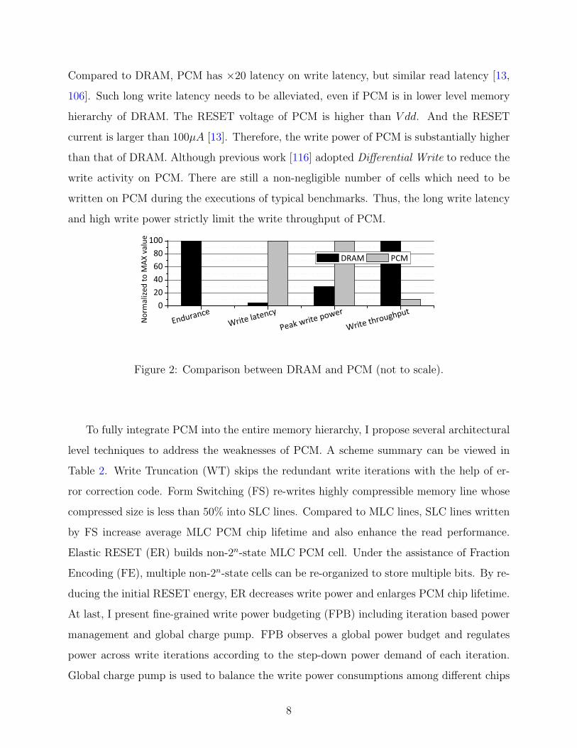
Compared to DRAM, PCM has ×20 latency on write latency, but similar read latency [13,
106]. Such long write latency needs to be alleviated, even if PCM is in lower level memory
hierarchy of DRAM. The RESET voltage of PCM is higher than V dd. And the RESET
current is larger than 100µA [13]. Therefore, the write power of PCM is substantially higher
than that of DRAM. Although previous work [116] adopted Differential Write to reduce the
write activity on PCM. There are still a non-negligible number of cells which need to be
written on PCM during the executions of typical benchmarks. Thus, the long write latency
and high write power strictly limit the write throughput of PCM.
EnduranceWrite latency
Peak write power
Write throughput0
20406080
100
Norm
alize
d to
MAX
val
ue
DRAM PCM
Figure 2: Comparison between DRAM and PCM (not to scale).
To fully integrate PCM into the entire memory hierarchy, I propose several architectural
level techniques to address the weaknesses of PCM. A scheme summary can be viewed in
Table 2. Write Truncation (WT) skips the redundant write iterations with the help of er-
ror correction code. Form Switching (FS) re-writes highly compressible memory line whose
compressed size is less than 50% into SLC lines. Compared to MLC lines, SLC lines written
by FS increase average MLC PCM chip lifetime and also enhance the read performance.
Elastic RESET (ER) builds non-2n-state MLC PCM cell. Under the assistance of Fraction
Encoding (FE), multiple non-2n-state cells can be re-organized to store multiple bits. By re-
ducing the initial RESET energy, ER decreases write power and enlarges PCM chip lifetime.
At last, I present fine-grained write power budgeting (FPB) including iteration based power
management and global charge pump. FPB observes a global power budget and regulates
power across write iterations according to the step-down power demand of each iteration.
Global charge pump is used to balance the write power consumptions among different chips
8
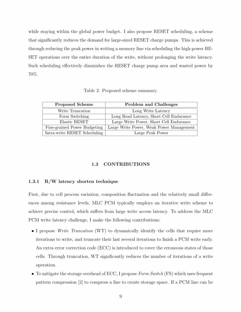
while staying within the global power budget. I also propose RESET scheduling, a scheme
that significantly reduces the demand for large-sized RESET charge pumps. This is achieved
through reducing the peak power in writing a memory line via scheduling the high-power RE-
SET operations over the entire duration of the write, without prolonging the write latency.
Such scheduling effectively diminishes the RESET charge pump area and wasted power by
70%.
Table 2: Proposed scheme summary.
Proposed Scheme Problem and Challenges
Write Truncation Long Write Latency
Form Switching Long Read Latency, Short Cell Endurance
Elastic RESET Large Write Power, Short Cell Endurance
Fine-grained Power Budgeting Large Write Power, Weak Power Management
Intra-write RESET Scheduling Large Peak Power
1.3 CONTRIBUTIONS
1.3.1 R/W latency shorten technique
First, due to cell process variation, composition fluctuation and the relatively small differ-
ences among resistance levels, MLC PCM typically employs an iterative write scheme to
achieve precise control, which suffers from large write access latency. To address the MLC
PCM write latency challenge, I make the following contributions:
• I propose Write Truncation (WT) to dynamically identify the cells that require more
iterations to write, and truncate their last several iterations to finish a PCM write early.
An extra error correction code (ECC) is introduced to cover the erroneous states of those
cells. Through truncation, WT significantly reduces the number of iterations of a write
operation.
• To mitigate the storage overhead of ECC, I propose Form Switch (FS) which uses frequent
pattern compression [2] to compress a line to create storage space. If a PCM line can be
9

compressed to less than half of its size, it can be stored in SLC form rather than two-
bit MLC form. Since SLC PCM has shorter access latency and better write endurance
than MLC PCM, accessing the line as SLC form accelerates performance critical read
operations.
• I evaluate the designs in a hybrid DRAM-PCM main memory architecture, and compare
them to state-of-the-art designs, such as write pausing [81] and MLC compression [97].
The results show that the designs reduce the effective write and read latencies by 57%
and 28% respectively, and achieve 26% performance improvement over the state of the
art.
1.3.2 Cell endurance enhancement and write power reducing technique
Second, a larger PCM RESET energy significantly shortens cell endurance [37, 58]. To ad-
dress this problem, I propose elastic RESET (ER) to construct non-2n-state MLC PCM.
By reducing the RESET energy, RESET power is effectively reduced and PCM lifetime is
prolonged. The existing work that is most close to my design is MLC-to-SLC transfor-
mation [5, 51] that compresses and stores highly compressible PCM lines in SLC format.
MLC-to-SLC transformation is only applicable if a line is highly compressible, i.e., the com-
pressed size is ≤ half of the original size. Unfortunately, many applications have 60%∼75%
compression ratio and thus cannot benefit much from it. The contributions are summarized
as follows.
• I propose Elastic RESET (ER) that reduces RESET current to construct non-2n-state
MLC PCM. ER effectively reduces the RESET energy such that it can extend PCM
endurance exponentially.
• I propose Fraction Encoding (FE) to store compressed data using non-2n-state MLC
PCM cells. Instead of storing multiple bits in one cell, FE combines multiple cells to
store multiple bits, e.g., 2 cells to store 3 bits, and thus can adaptively store compressed
data with relaxed compression ratio.
10

• I evaluate my proposed designs and compare them to related works in the literature.
The experimental results show that ER improves PCM chip lifetime by ×32 and reduces
RESET power by 17% on average.
1.3.3 Write throughput improvement technique
Previous power budget scheme [40] allocating the same power budget for all iterations in a
MLC line write is often too pessimistic. A MLC PCM write has one RESET pulse and a
varying number of SET pulses. The RESET pulse is short and of large magnitude while the
SET pulse is long and of low magnitude. In addition, when writing one PCM line, most cells
in the line require only a small number of SET pulses [51]. Allocating power according to
the RESET power request and for the duration of the longest cell write is power inefficient.
Moreover, one heavily written (hot) PCM chip may block the memory subsystem even
though most memory chips are idle. This phenomenon arises because the power that each
chip can provide is restricted by the area of its charge pump. When multiple writes compete
for a single chip, some writes have to wait to avoid exceeding the charge pump’s capability.
Otherwise, cell writes become unreliable. So, I propose two new fine-grained power budgeting
(FPB) schemes to address these problems:
• FPB-IPM is a scheme that regulates write power on each write iteration in MLC PCM.
Since writing one MLC line requires multiple iterations with step-down power require-
ments, FPB-IPM aims to (i) reclaim any unused write power after each iteration and (ii)
reduce the maximum power requested in a write operation by splitting the first RESET
iteration into several RESET iterations. By enabling more MLC line writes in parallel,
FPB-IPM improves memory throughput.
• FPB-GCP is a scheme that mitigates power restrictions at the chip level. Instead of
enlarging the charge pump in an individual PCM chip, FPB-GCP integrates a single
global charge pump (GCP) on a DIMM. It dynamically pumps (boosts) extra power
to hot chips in the DIMM. Since GCP has lower effective power efficiency (i.e., the
percentage of power that can be utilized to write cells), I consider different cell layout
optimizations to maximize throughput.
11
1.3.4 Peak power reduction technique
At last, high power consumption has become a major challenge in designing PCM based
memory systems [40, 48]. The working voltage needs to be boosted from 1.8V (Vdd) to 2.8V,
3.0V or even 5.0V for BJT, MOS- and diode-switched PCM respectively [8, 55, 61]. Those
high voltages are provided by different types of CMOS-compatible on-chip charge pumps
(CP) [73], which convert lower input voltage to higher output voltages. There are major
limitations to CPs in PCM chips. First, a CP typically consists of cascaded stages of large
capacitors and wide transistors, each stage elevating the voltage by a certain amount. Charg-
ing and discharging consume large parasitic power due to parasitic capacitance proportional
to those large capacitors [73, 107]. In addition, the leakage power of CPs is usually quite
large as a result of the wide, strong transistors and high voltages on internal nodes and the
output [107]. Also, CPs dissipate significant power on its own peripheral circuits such as
controls, drivers, clock generation and distribution. The parasitic, leakage and peripheral
circuit power are significant sources of power loss of CP. They can be termed as wasted
power in this work. This is also why the power conversion efficiency of CP, defined as the
ratio between output and input power, is usually very low. As low as 20% of efficiency has
been reported for a CP with current load in several PCM chips. To supply enough output
current, either larger input current of a single CP is needed, or more CP units are necessary.
As a result, CPs consume large chip area, e.g. ∼20% [61], as well. My evaluation shows that
the total power dissipated by the CPs accounts for more than 81% of the total memory power,
where 60% is due to just the parasitic power. Hence, it becomes increasingly important to
design effective schemes to reduce power loss of CPs. I propose one technique to tackle the
aforementioned main limitations to PCM CPs. My contributions are as follows.
• I propose RESET scheduling, a scheme that significantly reduces the demand for large-
sized RESET CPs. This is achieved through reducing the peak power in writing a memory
line via scheduling the high-power RESET operations over the entire duration of the
write, without prolonging the write latency. Such scheduling effectively diminishes the
RESET CP area and wasted power by 70%.
12

• I provide detailed CP modeling, and simulated my proposed techniques on MOS-, BJT-
, diode-switched PCMs. We also tested both SLC and MLC structures. The overall
reduction in wasted power are observed to be between 37%∼49% for different access
devices or cell designs. These results prove that the proposed technique are effective and
generally applicable to different PCM designs.
1.4 THESIS ORGANIZATION
The rest of this thesis is organized as follows. Chapter 2 presents preliminary information of
PCM. Chapter 3 discusses the related work. The MLC PCM latency reduction techniques
are presented in Chapter 4. Chapter 5 illustrates the MLC PCM cell endurance enhancement
schemes. The MLC PCM write power management techniques are summarized in Chapter 6.
Chapter 7 elaborates the peak power reduction technique in PCM chips. Chapter 8 concludes
the thesis.
13

2.0 BASICS OF PHASE CHANGE MEMORY
2.1 PCM FUNDAMENTALS
Phase change memory (PCM) is a type of non-volatile memory that stores information in
a phase change material such as a chalcogenide alloy. Figure 3 shows one example of PCM
array. A PCM cell usually consists of a thin layer of chalcogenide with two electrodes on
each side. The chalcogenide, such as Ge2Sb2Te5 (GST), has stable crystalline (logic “1”)
and amorphous states (logic “0”). Given the large resistance contrast between crystalline
and amorphous states, it is possible to exploit partial crystallization states to store more
than two bits per cell. This approach is referred to as multi-level cell (MLC) PCM. MLC
PCM uses smaller resistance ranges to represent different digital levels, which demands more
precise control to achieve reliable memory access.
2.2 PCM WRITE
As shown in Figure 4, there are two kinds of PCM write (or programming) operations [46]. A
SET operation heats the phase change material, GST, above the crystallization temperature
(300 C) but below the melting temperature (600 C) using a long but small current. A SET
operation writes the PCM cell into a logic ‘1’ (crystalline state). In contrast, with a short
and large current, the GST is melted and quenched quickly by a RESET operation, which
writes the PCM cell into a logic ‘0’ (amorphous state).
Writing MLC PCM cells exhibits significant non-determinism due to process variations
and composition fluctuation in nano-scale devices. As shown in Figure 5(a), the composition
14

W
bit
lin
e
wordline
a
X
Z
X0
He
Ht
H
GST
TiN Electrode
Si3N4
Heater
Figure 3: PCM cell array.
temperature
time
Melting Point (~600)
tsettreset
Glass Transition
Temperature (~300)
Figure 4: PCM RESET and SET.
15

of Ge, Sb, and Te in GST PCM has both inter- and intra- cell material fluctuations [10]. To
change a cell’s resistance level, a large RESET pulse is applied to form an amorphous cap
in the GST. After this step, SET pulses are applied to build the crystalline filaments in the
cap (Figure 5(b) and Figure 5(c)). The locations of filaments in GST are non-deterministic
although the same amount of crystalline volume can be used to represent the same resistance
levels. Studies have shown that the filament with slightly more Sb needs less crystallization
time [10]. Therefore, given the same SET pulse, different PCM cells, or the same cell at
different times, form different filaments in the cap. In addition, the heater size and peripheral
circuits also introduce variations to a PCM write [112, 49]. Due to these reasons, it is very
difficult for a single current pulse to precisely program a MLC to an intermediate state that
has small resistance difference from neighboring states.
Because a single pulse is impractical, an iterative program-and-verify (P&V) strategy is
widely adopted in both industrial prototypes [8, 69, 74] and academic research [14]. Given a
target resistance range, the write circuit heuristically determines the initial current param-
eters to program the cell. After the programming pulse, the circuit reads the cell resistance
and verifies whether the resistance falls in the target range. The write process completes
when the target range is reached. Otherwise, the circuit re-calculates the write parameters
and repeats the steps until the target range is reached or a predetermined maximum number
of iterations has been attempted without success.
Figure 6 illustrates a staircase-up P&V MLC programming scheme. This design sim-
plifies the hardware by using the same width for all current pulses, starting from an initial
RESET pulse. An alternative programming scheme uses one SET pulse and multiple RESET
pulses [52]. This scheme introduces reliability concerns, including resistance drift. It is also
difficult to control the melting process. Therefore, industrial prototypes and most studies
adopt the scheme in Figure 6. I also use the same mechanism, and assume that no write is
performed if the value does not change, a.k.a., Differential Write [116].
The number of iterations required to complete a particular MLC PCM write depends on
many factors, such as required programming precision, programming algorithm, and control
circuit design. Qureshi et al. from IBM TJ Watson developed a two-phase model [82] to
capture the P&V PCM programming strategy assuming the convergence probability of write
16

Te
Ge
Sb
Ge
Te
Te
SbGe
Sb
Sb Sb
Sb Te
Se Ge
Sb Te Sb Te
Ge Te
SbTe
Heater
(a) Composition fluctuation.
Amorphous
Cap
(b) RESET pulse.
Filaments
(c) SET pulse.
Figure 5: Non-deterministic PCM writes.
17

Voltage
Time
VReset
Vset,0
Vverify Vverify
Vset,1Vset,2
Vverify
...
Figure 6: Single RESET multiple SETs staircase-up P&V scheme.
iterations follows the Bernoulli distribution. The model considers both the learning phase
(the first several write iterations) and the practice phase, and computes the probability to
finish a MLC PCM cell write at iteration k as
P (k) =
F1 · (1− F1)k−1 if k ≤ i
F2 · (1− F2)k−i−1(1− F1)
i if k > i
(2.1)
where F1 and F2 indicate the expected probabilities of convergence at the k-th iteration
during the learning phase and the practice phase, respectively; i is the number of iterations
in the learning phase, and k is the count of write iterations. In the learning phase, the
convergence probability is relatively small, which indicates more tries are necessary. After
the learning phase, the write heuristic improves to have better convergence. This model was
validated [82] and shown to match real-world experiments on write operations [69].
2.3 PCM READ
Reading a PCM cell involves sensing its resistance level and mapping the analog resistance
to a corresponding digital value. For SLC PCM, this capability is achieved by comparing cell
resistance to a reference cell. The reference cell’s resistance is chosen as roughly the middle
18

of the whole resistance range. In Figure 7(a), when compared with a 500KΩ reference cell,
a larger resistance indicates the stored value is “0”. Otherwise, the value is “1”.
A read operation for a MLC commonly uses binary search. Figure 7(b) shows that, to
read a 2-bit MLC, the circuit first compares the resistance to a reference cell at 500KΩ.
Depending on the comparison outcome, the circuit next compares the resistance to 50KΩ
or 5MΩ. It then determines the stored value. In general, a read operation for a n-bit MLC
requires n iterations to complete.
‘1’ 10KΩ ‘0’ 10MΩ> Ref. 500KΩNo Yes
(a) SLC
‘11’ 10KΩ ‘10’ 100KΩ
> Ref. 50KΩNo Yes
‘01’ 1MΩ ‘00’ 10MΩ
> Ref. 5MΩYes No
> Ref. 500KΩNo Yes
(b) MLC
Figure 7: PCM read operation requires comparison to reference cells.
Given that reads are on the critical path, an aggressive design could perform all com-
parisons in parallel and complete the read in one iteration. For n-bit MLC PCM, parallel
sensing needs to duplicate the read circuit (2n-1) times. This represents a trade-off between
performance, increased sensing current and hardware overhead. As such, sequential sensing
is widely adopted for MLC PCM read [83, 16].
19

3.0 PRIOR ART
3.1 ERROR CORRECTING AND SALVAGE
Resistance drift and cross-talk are neglected on traditional single level cell (SLC) PCM as
described in [13]. For example, a SLC PCM cell, if it is written reliably, can retain data
for more than 10 years at 85oC. As such, PCM failures considered in this paper can be
immediately detected with read-after-write. Each line write is followed by a line read to
confirm if the data was correctly written. Recent work [113] [6] noticed that resistance
drifting may produce soft errors on multiple level cell (MLC) PCM. However, by applying
anti-drifting encoding method and changing MLC pages to single level cell (SLC) pages,
resistance drifting problem can be controlled in a trivial level [113].
Unlike traditional SRAM, PCM is resilient to radiation induced transient faults. How-
ever, because of the large area of periphery circuitry in a PCM chip, soft errors can still occur
on the periphery, such as row buffers and interface logic. Free-P [111] deployed a 61-bit 6
bit-error correcting 7 bit-error detecting (6EC-7ED) BCH code for each 64-byte memory line
to prevent potential soft errors. Device and circuit community have a more straightforward
way to eliminate soft errors on periphery circuitry by ECC or parity before buffering the
data, exchanging parity bits during bus transmissions [71] and reissuing requests in the case
of a error. Therefore, no additional storage overhead within the PCM data array is required
for protection against soft errors.
To change state, a bit cell is heated and cooled by applying different currents (RESET
and SET current). Due to repeated heating, a PCM cell can be reliably written only a
limited number of times, which is referred to as write endurance. While an individual PCM
cell can handle 1012 write cycles [58], experiments with PCM to arrays and chips have shown
20

much lower endurance in the range of 107−109 writes [13, 45]. Write endurance is significant
obstacle that restricts PCM from serving as an immediate and widespread replacement for
DRAM.
Wear-leveling aims to postpone the appearance of cell failures by spreading and balancing
write operations [84, 93, 116, 34] among all usable cells/lines. Early table-driven wear-
leveling techniques [116, 33] require OS management to periodically swap data stored in
different regions based on write activity. To achieve better trade-offs, write frequencies
are often recorded at a coarse-granularity in the table. Recently proposed wear-leveling
techniques build a randomized mapping between physical address (PA) and PCM device
address (DA) [84, 93]. In these designs, one PA may be mapped to different DAs at different
times. The mapping is managed by simple hardware (including several registers and control
circuit) and is hidden from the OS and user applications.
To accommodate relatively high cell failures, PCM devices include spare lines and use
built-in hardware support to automatically remap failed lines to spares early in a chip’s
lifetime (i.e., with a small number of failures). Two types of hardware designs may be
adopted. One design re-wires the address decoding logic (similar to a large capacity cache
design [3]) and the other uses a small remapping table. Both designs incur large hardware
overhead, and thus, can only support remapping a small number of failed lines. For example,
Qureshi et al. [84] integrates a spare line buffer that can remap 5% of total lines. The benefits
of built-in spare-line replacement are: it is transparent to upper level designs, user visible
PCM space is contiguous, and access latency is little affected.
Salvaging techniques [91, 44, 94, 111] try to continue the duty cycle of PCM chips that
have even a significant amount of failed cells, e.g., Ipek et al.[44] can tolerate up to one half
of all pages failing. Salvaging techniques gracefully degrade in accordance with the number
of failed cells, which is a significant difference to built-in spare line replacement that masks
failures. To study the salvaging result in the later stage of lifetime of PCM chip, we adopt
ECP [91] as our salvaging baseline. Given a 512-bit (64B) line, ECP saves six 9-bit pointers
and corresponding 1-bit data in extra storage that was traditionally used to hold ECC infor-
mation. Each pointer can fix any failed cell within a 64B line. ECP significantly improves
PCM lifetime over ECC and other error correction techniques. SAFER [94] dynamically
21

divides broken bits into different groups within one 64-byte memory line. However, only
2% extra lifetime improvement over ECP was achieved by SAFER [94], therefore, we choose
ECP as our baseline. We also compare LLS with FREE-p [111], which is memory line level
remapping salvaging scheme.
3.2 REDUCING EFFECTIVE READ LATENCY
There are different approaches to address the long latency write problem. By merging
frequent writes within the DRAM cache, the number of writes issued to a PCM device
can be greatly reduced [85]. Write pausing [82] allows performance critical read operations
to preempt writes. Comparing to morphable memory system [83] that also converts MLC
lines to SLC lines, FS is data-centric and transparent to higher system layers, including the
operating system.
In a DRAM and PCM hybrid main memory system, cache replacement policy [114] and
cache partition algorithm [115] are also proposed to move more write traffic to DRAM and
read intensive lines to PCM. In this way, both short read latency and short write latency
can be guaranteed.
3.3 COMPRESSION ON PCM
Compression has been applied in PCM to reduce the total number of bits writing to the cells.
Compressed data with a smaller size can be written into fewer PCM cells than original data.
Comparing to compression-only designs [97, 112], FS stores highly compressible lines in
SLC form using the same location such that it reduces the read accesses while [97] target at
improving lifetime and energy only. Compression techniques [29] are also adopted to improve
the small write bandwidth of PCM based or DRAM and PCM hybrid main memory system.
22

3.4 PROCESS VARIATION AND OVER-RESET
For PCM chips with billions of cells, some cells tend to fail earlier than others. One variation
source is the difficulty in controlling physical feature size in a nano-scale regime [112]. Due
to these variations, different cells have different optimal RESET current values. A cell
suffers from OVER-RESET if a current higher than its optimal value is used. An early
report showed that every 10× increase in pulse energy results in 1000× lower endurance
[58]. Recent measurements of failure rates on fabricated PCM chips showed similar results -
10× more failures were observed when a cell is 60% overheated [58]. While strong systematic
process variations (PV) might be mitigated through circuit design, e.g., current provision
[112, 49] or customized write circuit, there are still non-negligible variations at the chip level.
The impact of process variation on several parameters, such as gate length and Joule
heater’s radius, is analyzed in [112]. In [112], the distribution of RESET currents is generated
by one dimensional heat model. This work selects the worst case in a 4MB block as the
RESET current. Several other techniques, like Frequent Pattern Compression and page
classification, are also adopted in [112] to increase PCM chip lifetime. However, too large
systematic process variation is modeled in [112], while the latest works [44] [91] [94] observe
no significant systematic process variation on PCM. Therefore, without the presence of large
systematic process variation, employing the worst case RESET current in a 4MB size block
may not be effective in increasing PCM lifetime.
3.5 PCM WRITE POWER MANAGEMENT
High write power is known as a major disadvantage of PCM. Schemes have been proposed to
change only the cells that need to be changed [116, 60]. Cho et al. proposed flip-n-write that
can pack two line writes with the power budget of writing the number of one line cells [20].
It has limited benefit for MLC PCM due to the additional states used in MLC PCM. Hay et
al. proposed to track/estimate bit changes in the last level cache and issue write operations
as long as the DIMM level power budget can be satisfied [40]. Du et al. presented a novel
23

bit mapping scheme to distribute hot bits evenly into all PCM chips [30]. In this way, the
chip level power constraint introduced by charge pump can be overcome, so that no hot chip
will block the following writes [30]. These power management schemes focus mainly on SLC
PCM. The FPB schemes proposed in this paper address MLC PCM write by exploiting its
characteristics.
To address write power in MLC PCM, Joshi et al. proposed a novel programming method
that decreases write energy and latency by switching between two write algorithms: single
RESET multi-SET and single SET multi-RESET [52]. The latter is often less reliable.
Wang et al. proposed to reduce write energy by adopting different mappings between data
values and resistance levels [101].
3.6 MLC PCM
MLC PCM can effectively reduce per bit fabrication cost. Schemes have been proposed to
address its latency, write energy, and endurance issues [83, 81, 51]. MLC PCM differs from
SLC PCM in that it has non-negligible resistance drift problem. Zhang et al. proposed
different encoding schemes to mitigate drift [113]. Awasthi et al. proposed lightweight
scrubbing operations to prevent soft errors [6].
3.7 ASYMMETRIC WRITE
The RESET and SET operations have asymmetric characteristics in terms of latency and
power [88]. Most previous work did a RESET followed by a sequence of SETs. Qureshi
et al. proposed to perform SET operations before the memory line is evicted from last-
level cache [80]. When a write operation comes, only the short-latency RESET needs to be
performed. However, PRESET faces difficulty on MLC PCM as MLC uses more resistance
levels, which prevents PRESET the line to one state.
24

3.8 PCM CHARGE PUMP DESIGN
Recent chip demonstration [22] proposed write charge pump pre-emphasis to accelerate the
charging operation by providing a group of auxiliary RESET and SET CPs. In order to boost
the write pumps faster, more area overhead and leakage for extra pumps have to be paid.
25

4.0 MLC PCM WRITE LATENCY REDUCTION
4.1 MOTIVATION ON MLC PCM LONG WRITE LATENCY
Observation: Uneven Distribution of MLC PCM Write Iterations: The staircase-
up P&V MLC programming scheme uses multiple iterations to precisely program a PCM
cell. Since each current pulse has the same width, the write latency is then determined by
the number of iterations. When writing a PCM line, different cells require a different number
of iterations. While the majority of cells likely finish in a modest number of iterations, some
cells can take more iterations. Thus, the completion time of the whole line is determined by
the cell that requires the largest number of iterations. In this section, I define the cells that
require more iterations as a difficult-to-write cell set.
Definition 4.1.1. When writing a PCM line segment that has n cells, its difficult-to-write
cell set is the subset of m cells that require the same or more iterations than the other cells.
The cells in the difficult-to-write cell set require a certain number of iterations only for a
particular write instance. Therefore, the difficult-to-write set membership may change from
write to write.
Definition 4.1.2. When writing k PCM line segments (each has n cells), the difficult-to-
write cell set is all m difficult-to-write cells in each segment, i.e., it consists of k ·m cells.
If n equals the number of cells in one PCM line, then the difficult-to-write cell set refers
to the cells that globally require more iterations than other cells. If a PCM line is divided
into k segments, then the difficult-to-write cell set refers to all m difficult-to-write cells in
each segment. In this section, I choose n=64 and m=1; k varies depending on the size of
the PCM line.
26

The completion time of the whole line is determined by the cell that requires the largest
number of iterations. Moreover, the difficult-to-write cell set and the most difficult-to-write
cell vary from one write to another due to non-determinism in changing device resistance,
e.g., the growth of filaments, as explained in Section 2.2. Hence, such a set cannot be
predicted and precluded before or during an early stage of the write. For example, for the
same PCM line, its 1st and 2nd cells are difficult-to-write in one write, while its 3rd and
4th cells may become difficult-to-write in the next write. Similarly, the same MLC line may
require only two iterations in one write instance, but then it requires eight iterations in
another write instance.
1 2 3 4 5 6 7 8 9 10 110
100
200
300
400
401 246 239 7941 14 1111
# of
MLC
PCM
cel
ls
# of write iteratons
Figure 8: The distribution of the number of iterations.
Figure 8 plots the distribution of the number of iterations in writing a PCM line of 1024
2-bit MLCs, i.e., writing a 256-byte PCM line. This write finishes in 11 iterations. However,
not all lines require this many iterations. Some may require fewer and others may require
more. As discussed previously, a write to the same PCM line at different times may also
require different number of iterations.
As Figure 8 shows, only one cell needs 11 iterations. The majority of cells finishes in less
than 4 iterations. A few cells finish in 4-6 iterations. And only 4 cells require more than 6
iterations. When choosing (n=1024, m=4), these 4 cells form the difficult-to-write cell set for
this write instance. If the excessive iterations can be avoided for the difficult-to-write cells,
the line write latency can be reduced from 11 to 6 iterations, which is a 45% improvement
for this line write instance1.1Choosing (n=1024, m=6) would include these 4 cells and 2 other cells that require 6 iterations. For this
particular example, removing 6 difficult-to-write cells would have the same latency improvement as removing4 cells.
27

It is challenging to integrate MLC PCM in the memory hierarchy due to its longer
access latencies than SLC PCM. Qureshi et al. modeled MLC PCM access, and proposed
write cancellation (WC) [82] and write pausing (WP) [82] to let read operations preempt
long latency write operations. These techniques reduce the effective read latency of MLC
PCM. Qureshi et al. further proposed a morphable memory system [83] to improve the read
latency of MLC PCM by converting one MLC PCM page into two SLC pages when there
is sufficient memory. Sun et al. [97] proposed to compress data in MLCs for endurance and
energy benefits.
MLC PCM usually adopts iterative program-and-verify (P&V) to achieve precise resis-
tance control [8, 83, 14]. However, I observed that most cells can be reliably written in a
modest number of iterations, there are typically a small number of cells that require signif-
icantly more iterations. The cell that requires the largest number of iterations determines
the completion time of one write operation.
4.2 WRITE TRUNCATION
To prevent a few number of difficult-to-write cells from unnecessarily prolonging a write, I
propose write truncation (WT) to truncate the trailing iterations of those cells. As a result,
the difficult-to-write cells are temporarily failed since their writes did not finish. I apply single
error correction, double error detection (SECDED) ECC to correct these soft errors. Note
that the original line needs a mechanism to protect it from hard errors due to permanent cell
damage. I assume error correction pointer (ECP) [91] is used, as illustrated in Figure 9(a).
Hence, there are two sets of protection bits per PCM line: one for WT and the other for the
baseline error protection.
Figure 9(b) illustrates a line in my WT design. I choose (n=64, m=1), i.e., the difficult-
to-write cell set consists of the cell that requires the largest number of iterations in each 64
cell (128-bit) segment. For a 256B PCM line, there are 32B of ECP (64b per 512b block
as in the original design [91]), and 18B of SECDED ECC (9b per 128b block). Hence, the
extra space overhead of WT is 18B per 256B line.
28

Data in PCM Line
32 Bytes256 Bytes
ECP
(a) PCM line in baseline.
Data in PCM Line
32 Bytes256 Bytes
ECP ECC
18 Bytes
1 20 127...
ECC128 Bits per Section 9 Bits
(b) PCM line with WT.
Figure 9: Adding ECC to PCM lines for write truncation (WT).
The procedure of a write with WT is the following. When a line arrives, ECCs are
computed, and written with the line using iterative P&V. At the end of each iteration, the
write circuit checks in each 128-bit block (64 cells) how many cells are still being written. If
there is only one cell left, the verification step tests if the current state is only one bit away
from the target, such that ECC can cover this error. The write for this block is considered
finished if the condition is true, and the full write can complete if all sub-writes are finished.
Figure 10 summarizes my modifications to the existing P&V programming scheme. The
SECDED ECC can rescue one bit per 128 bits (64 cells) and more write iterations are
required if the condition is not satisfied. I adopt a gray code such that more write iterations
bring the resistance closer to the target level without increasing the number of bit differences.
Discussion: One problem with WT is that if a hard fault occurred in a line, the faulty
cell will become the dictating difficult-to-write cell since it can never be written no matter
how many iterations are used. This will deplete the opportunity of WT. Typically, when a
cell cannot be programmed to the target resistance range in a preset maximum number of
iterations (MAX), then the cell is identified as a hard fault which is rescued by ECP. However,
WT may terminate the write before MAX is reached, so that the hard fault is covered by
29

Target RLoad Default Initial
Parameters
Write
Read Resistance
Is Resistance in Target
Bandwidth? OR
Can ECCs cover Current error?
(Write Truncation)
Calculate New
Slop and Load
No
Yes
Finish
Serving Pending
Read Request
(Write Pausing)
Figure 10: P&V programming with write truncation (WT).
ECC, rather than ECP. This problem can be solved through wear-leveling techniques such
as start-gap [84]. Wear-leveling will guarantee that periodically, all lines are swapped within
a region. WT can be disabled during wear-leveling to permit the writing of cells with hard
faults to reach MAX. This process guarantees that cells with hard faults are discovered and
marked by ECP bits. ECC will only cover non-faulty cells, continuing to provide short write
latencies in the presence of hard faults.
Unlike ECC in DRAM, which corrects soft errors, ECC for WT is not intended to cover
soft errors: PCM is naturally resilient to them. DRAM ECC is designed to achieve a certain
reliability level. It may fail with a slim probability that there are more errors than it can
handle, while my ECC guarantees to correct one “soft error” (from a difficult-to-write cell).
The advantage of using ECC over other error-correction mechanisms, such as ECP, is
that ECC can be generated regardless of the positions of difficult-to-write cells. This property
is desirable because ECC can be generated before a write operation starts, which enables
writing the data and ECC simultaneously. As a comparison, ECP uses pointers to record
the locations of the cells to rescue. Since these locations can only be known when a write
operation almost completes, ECP can only be generated at that time. Using ECP would
actually prolong the write operation. Therefore, ECC is adopted in my design.
30

Figure 10 also illustrates a recent write optimization for MLC PCM: write pausing [81].
This optimization allows reads to preempt long-latency write operations to avoid being
blocked for a long time. WT is orthogonal to write pausing as the latter does not reduce
the bank level service time for each write. WT allocates more service time for reads such
that system performance is improved when memory accesses are intensive. With WT, MLC
PCM write operations may have different programming iteration numbers and different write
latencies. Without increasing the the complexity of memory controller, PCM chips can
handle different write latencies with the new proposed framework and protocol in [31].
4.3 FORM SWITCH
Although WT reduces the number of write iterations, it adds 9 bits per 128-bit PCM line
segment, which corresponds to 7% storage overhead. In this section, I propose form switch
(FS) to remove the storage overhead. FS compresses data to create space for storing ECC
and transparently stores highly compressible lines in SLC form to reduce read latency.
FS employs frequent pattern compression [2] (FPC) to compress each MLC line. FPC
examines every word and transforms frequently used patterns into fewer data bits and a
prefix. A hardware compression unit is integrated in the memory controller to compress a
line before it is stored in PCM. This compression unit also decompresses a line on a read. The
experimental section shows that the compression unit’s latency, area, and energy overhead
are negligible.
I use the following configurations in FS with FPC. The baseline has 256 bytes of MLC,
with 32 bytes of ECP and 18 bytes of ECC. When a line is compressed with FPC, the write
circuit generates 9-bit ECC for every 128-bit block of a compressed line. For example, suppose
a line is compressed to 64 bytes, only 36 bits (=(64×8/128)×9) of ECC are generated, instead
of the full 18 bytes. This saves space. The ECP bits are not affected.
After compression, if the total number of bits of the compressed data, prefix tag, and
ECC is 128 bytes or fewer, then FS treats MLC as SLC. That is, every cell stores only one
bit of information. This form switch not only speeds up writes, but also improves reads as
31

Compressed Data
32 Bytes256 Bytes
ECPECC
18 Bytes
(a) Data field with enough space
Compressed Data
32 Bytes256 Bytes
ECPECC
18 Bytes
(b) Data field with not enough space
Uncompressed Data
32 Bytes256 Bytes
ECPECC
18 Bytes
(c) Data field without any space
Figure 11: Integrated form switch with write truncation.
32

only one comparison round to the reference resistance is performed. In addition, FS also
benefits endurance as SLC experiences much less stress during writes than MLC. I use 1 bit
per line as a flag to indicate the line form. When the bit is set, the PCM line is used as an
SLC line. Otherwise, it is an MLC line.
If the total number of bits including data, tag and ECC is more than 128 bytes, then
they are stored in MLC form, i.e., form switch is not used. In this case, there is a possibility
for the total bit count to exceed 256B. If this happens, I borrow ECP bits since they are
useful only when hard faults occur, as shown in Figure 11. Finally, if the ECP field is full
and I cannot borrow bits to store ECC, then FS disables ECC protection, WT returns to a
baseline write mechanism.
Discussion: To mitigate write imbalance within one line, intra-line rotation [91] evenly
distributes writes to both data and ECP cells. I adopt the same design to balance writes
in one line. However, even with intra-line rotation, WT still tends to degrade PCM chip
lifetime as including extra ECC bits increases the number of bits to be written. Compared
to data bits, ECC bits are more likely to change as they are computed from data bits. I next
study WT’s impact in more details. First, when adopting differential write [116], on average
for each write, only about 15% data bits are changed and need to be written. Figure 12
compares the bit changes before and after adopting WT. MLC-C-M represents a scheme that
compresses the data (no ECC) and stores it in MLC form. MLC-C-ECC represents FS + WT
that compresses data: if the size of compressed data and ECC reduces to half, then lines are
stored in SLC form; otherwise, the compressed data and ECC are stored in MLC form. As
shown, there is a slight decrease for the bit changes: it is about 2% on average.
In experiments, I observed on average FPC achieves 50% compression rate. However,
approximately only 20% of all lines are highly compressible, i.e., the lines can be written in
SLC form. I also studied the lifetime impact after integrating the extra ECC. It was reported
that storing data bits in compressed form reduces the total number of writes to the device,
and thus, improves lifetime [112, 97]. Figure 13 compares the lifetime change after applying
FS. Compared to the baseline without compression, FS also improves lifetime as fewer bits
are changed. Compared to the compression only design (using FPC), FS tends to reduce
lifetime as more bits are changed; however, highly compressible lines are stored in SLC form
33

art gccbwa
ves
gemsFDT
D lbmlesli
e3d milcsphi
nx3 stream gmean
0.00.20.40.60.81.0
Re
dund
ency
Rat
e
SLC MLC(2-bit) MLC-C-M MLC-C-ECC
Figure 12: Write redundancy comparison when storing data in different forms.
and thus tend to extend lifetime. The latter is based on the assumption that SLC has longer
lifetime than MLC [83]. Similar studies for Flash showed that SLC has 10× better endurance
than MLC [98]. Therefore, lifetime is helped from the 20% highly compressible lines and
more benefits are expected when more lines are highly compressible. In Figure 13, FSLn
indicates SLC cell’s lifetime is n× MLC cell’s lifetime. For FSL10, I observed 7% lifetime
degradation.
ssca
stream
1
stream
2
stream
3
stream
4mix
1mix
2mix
3mix
4mix
5 lbmleslie3
dbw
aves
mcfgm
ean0.5
0.6
0.7
0.8
0.9
1.0
Life
time
Nor
mal
ized
to F
PC
FSL1 FSL2 FSL10
Figure 13: Lifetime degradation due to storing extra ECC bits.
This degradation is modest for two reasons: (i) limited PCM chip lifetime is due to
overprogramming [112]. While studies have reported up to 1012 cell endurance at the device
level [58], only 108 or lower endurance can be achieved at the chip level. Various circuit
level designs have shown great potential in mitigating overprogramming and extending chip
lifetime, e.g., 27× longer lifetime using current provision [112]. (ii) Improving MLC write
performance is much more difficult due to the precise control required for P&V programming.
34

Table 3: MLC PCM write latency reduction baseline configuration
System 8-core CMP, 4GHz
Processor Core single issue in-order, 32KB iL1, 32KB dL1
L2 (private) 2MB, 4-way, LRU, 64B/256B line size, write back
DRAM Cache 32MB, 8-way, 64B/256B cache line size,(private) 50ns (200 cycles) access latency, write back
Main Memory
32GB PCM, 4KB page, 4 ranks of 8-bank each,32 entries write queue/bank, 8 entries readqueue/bank, read priority scheduling (unless WRQis > 80% full), with differential write support
PCM Latency
SLC/MLC read: 125/250ns (500/1000 cycles); writeiteration: 250ns (1000 cycles); WT: 9b ECC covers128b/section; write model: F1 = 0.375, F2 = 0.625,i = 2 for ’01’, averagely 8 iterations; F1 = 0.425,F2 = 0.675, i = 2 for ’10’ (GC ’11’); averagely6 iterations; fixed 1 iteration for ’00’,fixed 2 iterations for ’11’ (GC ’10’)
4.4 MLC PCM WRITE LATENCY REDUCTION EXPERIMENTAL
METHODOLOGY
I used Virtutech Simics (with the g-cache and tran-staller module) to conduct experiments.
I assume an 8-core CMP system, which is similar to the architecture used in [81]. Like most
proposals, the baseline has a small DRAM cache to filter accesses to PCM. Table 3 gives
the baseline’s parameters. I modeled the cores in the CMP as single-issue, in-order pipelines
to accelerate simulations. The baseline system’s DRAM cache is 256MB and located off
chip. The DRAM cache uses a write-back policy with LRU replacement. It mitigates the
endurance problem by filtering write operations. The DRAM cache also merges hot writes,
which significantly reduces the write traffic to the PCM.
The baseline has a 32GB PCM memory that consists of 4 individual memory ranks. Each
rank has 8 banks with a 32-entry write queue (WRQ) and an 8-entry read queue (RDQ).
The PCM uses differential writes to store a value only when the new value differs from the
old one in a PCM cell. When a bank is idle, the oldest request in the highest priority queue
is issued to the bank. In general, the read queue has a higher priority than the write queue.
35

Table 4: MLC PCM write latency reduction simulated applications
Benchmark Description RPKI WPKI
ssca m 8 copies of ssca 7.3 3.58
mcf m 8 copies of mcf 6.59 2.88
bwaves m 8 copies of bwaves 10.65 4.39
lbm m 8 copies of lbm 8.91 4.05
leslie3d m 8 copies of leslie3d 6.7 2.32
stream1 m 8 copies of COPY 9.94 3.28
stream2 m 8 copies of SCALE 9.91 4.9
stream3 m 8 copies of SUM 8.6 4.2
stream4 m 8 copies of TRIAD 11.15 3.64
mix 1 2lbm-2leslie3d-2mcf-2COPY 7.9 3.1
mix 2 2lbm-2leslie3d-2COPY-2TRIAD 9 2.25
mix 3 2lbm-2mcf-2COPY-2TRIAD 8.98 3.43
mix 4 2leslie3d-2mcf-2COPY-2TRIAD 8.36 2.99
mix 5 2lbm-2leslie3d-2mcf-2TRIAD 8.13 3.15
However, when the write queue is 80% full, its writes are serviced ahead of reads. I assume
the read latency of SLC PCM and MLC PCM are 500 cycles and 1000 cycles, respectively.
I determined that one write iteration is 1000 cycles from [81]. A write operation takes a
dynamic number of iterations to finish. The average write latency is ∼8000 cycles, which is
the same as [81].
I chose a set of memory intensive benchmark programs. These programs include lbm,
leslie3d, bwaves, mcf from SPEC2006, ssca from HPC Graph Analysis and a stream work-
load STREAM [68]. Table 4 summarizes the program’s memory access behaviors (read
MPKI and write MPKI). I executed the benchmarks in multi-programmed mode; each core
executes the same benchmark in a private space. In addition, I evaluated the performance of
mixed benchmark workloads. One mixed workload contains 4 different programs (2 copies
of each).
36

The write model: In this thesis, I adopt Qureshi’s model and extend it to reflect
that it takes a different average number of iterations to program a MLC to different digital
values [74, 52]. Gray coding (GC) is also included in my desgin. For example, in a 2-bit
MLC, the programming of a cell “00” (GC “00”) ends right after the RESET pulse. There
is no need for SET pulses. Programming the cell to “11” (GC “10”) also ends faster as a
slightly larger SET current can be applied. This slight overprogramming is safe as there
is no subsequent resistance level that needs to be differentiated. The bottleneck for a 2-
bit MLC write comes from programming “01” (GC “01”) and “10” (GC “11”), as shown
in [74, 52]. Here, I assume the average number of iterations to program “01” (GC “01”)
and “10” (GC “11”) are 8 and 6, respectively. This assumption is justified by previous
device-level experimental work [74].
To compare the effectiveness of different schemes, I use the following criteria. I define
effective read latency as following:
Effective Read Latency = trdready − trin, (4.1)
where trdready is the time when the PCM bank finishes servicing a read operation; and trin
is the time when the read operation reaches the read queue.
I define effective write latency similarly,
Effective Write Latency = twdready − twin, (4.2)
where twdready is the time when the write operation releases its corresponding PCM bank;
and twin is the time when the write request enters the write queue.
The speedup metric is defined as
Speedup =CPIbaselineCPItech
, (4.3)
where CPIbaseline indicates the CPI of the baseline machine, and CPItech is the CPI with
a proposed technique. The same speedup metric is used in [81]. It is also similar to the
weighted speedup.
37

I compared the following schemes in my experiments.
• WP — write pausing in [81]. It is enhanced with differential write.
• WP+FS — write pausing with form switch only (no extra ECC bits). This compares
my design to compression-only designs [97, 112].
• WP+WT — write pausing and write truncation.
• WP+WT+FS — write pausing, and write truncation and form switch (with extra
ECC bits).
To evaluate the impact on PCM chip lifetime, I collected memory write traces and did
my analysis on these traces assuming effective wear leveling [84].
4.5 MLC PCM WRITE LATENCY REDUCTION EVALUATION
4.5.1 WT and FS implementation overhead
I synthesized WT and FS in VHDL and report the latency, energy and area overhead in
Table 4.5.1. The overhead of WT comes from introducing extra ECC bits and the overhead
of FS comes from performing FPC compression. Given that MLC PCM read latency is
250ns, the latency overhead of WT and FS is less than 1% per access. The energy overhead
is less than 3 pJ per 64B line segment, which is negligible as reading and writing PCM
consumes 2 pJ/bit and 13 pJ/bit respectively [116] and one line segment contains 512 bits.
The area overhead is comparable to the area of a 16KB PCM when the PCM line is 256
bytes. This 16kb is negligible compared to the 32GB PCM in the baseline.
Table 5: The latency, energy and area overhead of WT and FS
OperationWT FS
En/Decoding Compress Decompress
Latency 0.5 ns 0.7 ns 1.2 ns
Energy (64B section) 0.7 pJ 1.2 pJ 2.1 pJ
Area (64B section) 14300 µm2 7300 µm2 18500 µm2
38
4.5.2 Effective write latency
Figure 14 compares the effective write latency using different schemes for 256B line size. I
normalized the results to the baseline. I report the results for 64B and 256B PCM line sizes.
Current systems often adopt 64B line sizes. However, with increasing capacity in the last
level cache (LLC), future systems are likely to adopt large line sizes to reduce tag overhead.
For example, IBM’s recently announced zEnterprise uses a 256B LLC line size.
For a 256B line, on average, write pausing (WP) experiences a 3% latency increase since
some writes are preempted and take more time to complete. Adopting FS, i.e., WP+FS,
decreases latency by 17% over the baseline as writing a line in SLC form is much faster
than in MLC form. The latency of compression and ECC encoding contributes less than 1%
overhead.
From Figure 14, write latency is reduced due to write truncation (WT). WT removes
the iterations that work on difficult-to-write cells as long as these cells can be corrected
using ECC bits. WT and WT+FS reduce write latency to 59% and 44% of the baseline,
respectively. An interesting observation is that WP+WT+FS’s reduction over WP+WT is
about the same as WP+FS’s reduction over WP, which indicates WT and FS are orthogonal
in reducing effective MLC write latency.
With 64B line size, I observed a larger latency increase (i.e., 10%) for WP as more writes
are preempted. WP+FS has a smaller latency reduction than the 256B line setting. The
reason is that the opportunity to compress a shorter line by 50% or more is smaller. WT
becomes more effective as more write instances benefit from reduced write iterations.
4.5.3 Effective read latency
Figure 15 compares the effective read latency using different schemes for 256B line size. On
average, WP improves read latency to 69% of the baseline. Since WT improves bank service
time, it is orthogonal to WP: adding WT further reduces the read latency to 59% of the
baseline. FS improves read latency by converting accesses to highly compressible MLC lines
to SLC accesses. This conversion is done at the architecture level, which is transparent to
upper levels, including the OS and user applications. When WP, WT and FS are applied
39

ssca_m
stream
1_m
stream
2_m
stream
3_m
stream
4_m mix1
mix2
mix3
mix4
mix5lbm
_m
leslie3
d_m
bwave
s_mmc
f_mgm
ean0.0
0.2
0.4
0.6
0.8
1.0
1.2
Nor
mai
lized
Ef
fect
ive
Writ
e La
tenc
y
WP WP+FS WP+WT WP+FS+WT
Figure 14: Effective write latency (256B).
together, read latency is dramatically reduced to 51% of the baseline, or 74% of WP’s read
latency. In some cases, e.g., bwaves m and stream2 m, I found FS by itself is more effective
than WT. This situation arises because more lines are highly compressible and converting
them to SLC form reduces read access latency.
While both WT+FS and FS benefit from accessing faster SLC cells, WT+FS is 18%
better than FS. This result happens because write pausing is disabled if a write operation
finishes more than 80% of one iteration. By reducing the write latency with WT, read
operations have fewer chances to be blocked by nearly-finished writes, and thus, they wait
less time in the queue. This further improves read latency in WT+FS.
When the PCM line size increases from 64B to 256B, fewer write operations are issued.
I observed larger read latency reduction as WP becomes more effective for 256B and helps
all schemes.
4.5.4 Performance analysis
By reducing both write and read latency, my designs improve program performance. The
results are summarized in Figure 16. For a 256B PCM line, WP has a 27% performance
improvement due to faster critical read operations. This result is slightly worse (but compa-
rable) to the result reported in [81]. My performance results for WP differ from the original
work slightly because I used differential writes to remove redundant cell writes, which in-
40

ssca_m
stream
1_m
stream
2_m
stream
3_m
stream
4_m mix1
mix2
mix3
mix4
mix5lbm
_m
leslie3
d_m
bwave
s_mmc
f_mgm
ean0.0
0.2
0.4
0.6
0.8
1.0
Nor
mal
ized
Effe
ctiv
e Re
ad L
aten
cy
WP WP+FS WP+WT WP+FS+WT
Figure 15: Effective read latency (256B).
creases the chance (by a small amount) that reads are blocked by writes. WP does not
achieve a noticeable performance improvement for stream3 m. In this program, the write
request ratio is high and the write requests come in a burst. WP is less beneficial in this
situation.
Figure 16 compares WP, WP+WT, and WP+WT+FS. The 256B results show that
WP+FS and WP+WT improve performance by 10% and 16% over WP respectively, and
WP+WT+FS gains another 9% performance over WP+WT. In total, WP+WT+FS has a
26% average performance improvement over WP, indicating WT and FS are orthogonal.
When the PCM line size increases from 64B to 256B, I observed 5% better performance
due to better performance from WP.
4.5.5 WT section size
In my design, I use 9 bits per 128 consecutive bits SECDED ECC. A 256-byte PCM line
is divided into 16 128-bit segments and requires 18-byte ECC that can rescue up to 16-bit
difficult-to-write cells. However, if two difficult-to-write cells appear in the same segment,
then the write operation cannot be terminated early as it is beyond the correction capability
of my ECC. The write circuit knows the number of difficult-to-write cells at the end of each
write iteration such that no error may exist as not correctable.
41

ssca_m
stream
1_m
stream
2_m
stream
3_m
stream
4_m mix1
mix2
mix3
mix4
mix5lbm
_m
leslie3
d_m
bwave
s_mmc
f_mgm
ean1.0
1.2
1.4
1.6
1.8
2.0
Speedu
p
WP WP+FS WP+WT WP+FS+WT
(a) 64B PCM line
ssca_m
stream
1_m
stream
2_m
stream
3_m
stream
4_m mix1
mix2
mix3
mix4
mix5lbm
_m
leslie3
d_m
bwave
s_mmc
f_mgm
ean1.0
1.2
1.4
1.6
1.8
2.0
Speedu
p
WP WP+FS WP+WT WP+FS+WT
(b) 256B PCM line
Figure 16: The IPC comparison of different schemes.
42

It is also possible to adopt a more powerful ECC, e.g., 8EC9ED (8-bit error correction
and 9-bit error detection) BCH ECC for all bits in a 256-byte PCM line. This code is a
global rescue design. Table 6 compares the number of ECC bits required for each PCM line,
the latency, and the area of three ECC codes. A 128-bit segmented ECC requires 0.5ns.
However, the global rescue scheme introduces non-negligible latency and area overhead.
Table 6: The comparison of different WT section sizes
Scheme Type Size Latency Area
64 bits section SECDED 32B 0.5ns ∼0.01 mm2
128 bits section SECDED 18B 0.5ns 0.0143 mm2
global rescue 8EC9ED 12B 30 - 80ns 1mm2
ssca_m
stream
1_m
stream
2_m
stream
3_m
stream
4_m mix1
mix2
mix3
mix4
mix5lbm
_m
leslie3
d_m
bwave
s_mmc
f_mgm
ean0.0
0.2
0.4
0.6
0.8
1.0
Nor
mal
ized
Perf
orm
ance
64/Section 128/Section
Figure 17: The comparison of IPC using different ECC codes.
I evaluated the performance impact of using SECDED. Figure 17 compares the perfor-
mance of three codes. I normalize the results to global rescue. In my simulation, I did not
count the encoding and decoding delay of global rescue. The performance differences between
global rescue and the other two schemes depends only on the ability to cover difficult-to-write
cells. 64-bit SECDED has a 2.1% performance improvement over 128-bit SECDED. However,
it requires 32 bytes per line while 128-bit SECDED requires only 18 bytes.
4.5.6 Iteration latency
In previous experiments, I set the average write latency to be the same as [81], which
used 1000 cycles per iteration. The iteration latency depends on material characteristics
43

and technology advances. I varied the latency from 500 CPU cycles to 1500 CPU cycles.
Figure 18 summarizes the change in IPC as this latency is changed. From the figure, WT +
FS + WP has higher speedup with longer iteration latencies. My schemes, WT + FS, win
33% performance improvement over WP. With a small iteration latency, a write requires a
shorter bank service time, which leaves more service time for reads. Therefore, removing
write latency and the bank busy time has less benefit for read operations as iteration latency
is decreased, and a diminishing improvement of program performance. But WT + FS +
WP still gain extra 13% performance over WP.
ssca_m
stream
1_m
stream
2_m
stream
3_m
stream
4_m mix1
mix2
mix3
mix4
mix5lbm
_m
leslie3
d_m
bwave
s_mmc
f_mgm
ean1.0
1.1
1.2
1.3
1.4
1.5
Speedu
p
500 750 1000 1250 1500
Figure 18: IPC comparison of WP+WT+FS with varying iteration latencies.
4.5.7 Sensitivity to write model
To my best knowledge, the PCM write model in [82] is the only available model describing
the PCM write convergence probability in different write iterations. The write convergence
probability can be represented by the Bernoulli distribution. The write model includes a
learning phase and a practice phase. Different phases have different convergence probabil-
ities. In original write model, the convergence probabilities in the learning phase (F1) and
the practice phase (F2) are 0.375 and 0.625. The write operation parameters in the learning
phase are produced by heuristic conjecture and will be modified based on the write results
in the learning phase. The learned writing parameters enhance the write convergence prob-
ability in the practice phase. And thus, F2 is usually larger than F1. With the development
of PCM material, we anticipate that the write convergence probability in the learning phase
increases, since more advanced PCM material is easier to write. And the write convergence
44

probability in the practice phase decreases, due to the more significant process variation and
material composite variation in deep sub-micron technologies. Therefore the write conver-
gence probabilities in the learning phase and the practice phase incline to become close to
each other.
0 2 4 6 8 10 12 14 16 18 200.0
0.2
0.4
0.6
0.8
1.0W
rite
Succ
ess %
Write Iteration #
0.125/0.875 0.25/0.75 0.375/0.635 0.5/0.5
Figure 19: Cell write iteration numbers with different F1/F2s.
0.125/0.875 0.25/0.75 0.375/0.625 0.5/0.51.0
1.5
2.0
2.5
3.0
Figure 20: The average cell write iteration numbers per line write.
The cell write iteration number per line write with different write convergence proba-
bilities is shown in Figure 19. With a larger convergence probability in the learning phase,
more cells finish their writes in the first several iterations. Therefore, as Figure 20 shows
that the average write iteration number for all cells in one write decreases substantially.
With a smaller convergence probability in the practice phase, the accurate memory write
45
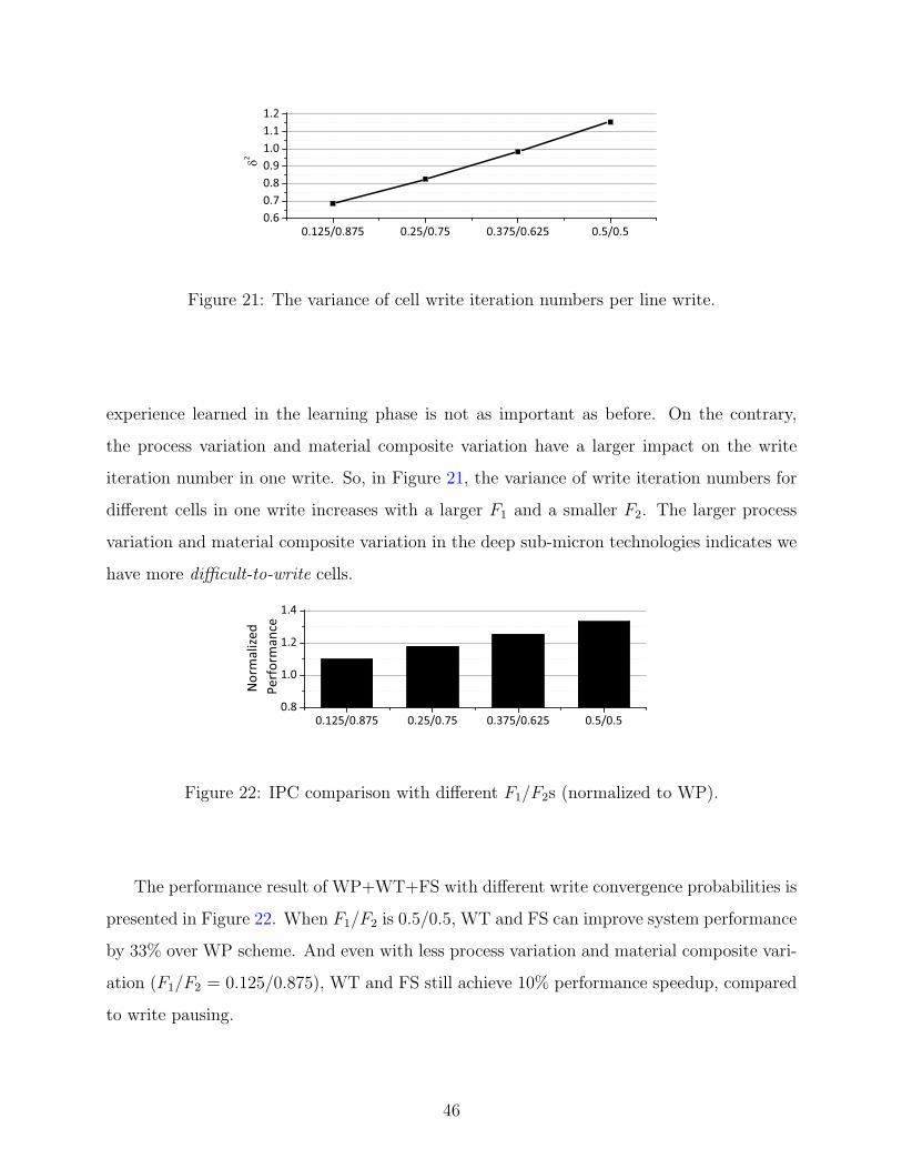
0.125/0.875 0.25/0.75 0.375/0.625 0.5/0.50.60.70.80.91.01.11.2
2
Figure 21: The variance of cell write iteration numbers per line write.
experience learned in the learning phase is not as important as before. On the contrary,
the process variation and material composite variation have a larger impact on the write
iteration number in one write. So, in Figure 21, the variance of write iteration numbers for
different cells in one write increases with a larger F1 and a smaller F2. The larger process
variation and material composite variation in the deep sub-micron technologies indicates we
have more difficult-to-write cells.
0.125/0.875 0.25/0.75 0.375/0.625 0.5/0.50.8
1.0
1.2
1.4
Nor
mal
ized
Perf
orm
ance
Figure 22: IPC comparison with different F1/F2s (normalized to WP).
The performance result of WP+WT+FS with different write convergence probabilities is
presented in Figure 22. When F1/F2 is 0.5/0.5, WT and FS can improve system performance
by 33% over WP scheme. And even with less process variation and material composite vari-
ation (F1/F2 = 0.125/0.875), WT and FS still achieve 10% performance speedup, compared
to write pausing.
46

5.0 MLC PCM ENDURANCE ENHANCEMENT
5.1 MOTIVATION ON MLC PCM SHORT CELL ENDURANCE
Comparing to SLC, MLC PCM suffers more severely from large RESET power and long
read/write latency problems. In order to reliably represent the stored logic value, a PCM
cell needs to have its resistance programmed within a tight resistance range. Since MLC
has more resistance levels to represent, it often has tighter resistance range per level and/or
higher maximum resistance, as shown in Figure 24. Given a PCM write circuit that has
certain programming precision, MLC PCM requires a larger RESET current than SLC PCM
to initialize its maximum resistance and contain more resistance levels.
mcf
libquantu
m astar
xalancb
mk milc bzip2 lbm wrf
gcc.200
igcc.
typegmean0.50.60.70.8
Com
pres
sion
Rat
io 32B 64B 128B
Figure 23: Compression ratio of all line-level writes.
~1KΩ ~100MΩMLC 011011 00 ~1KΩ SLC1 0~100KΩFigure 24: MLC has tighter resistance ranges.
47

However, larger RESET energy significantly shortens cell endurance. As revealed by
device studies [37, 58], 2× RESET energy results in 100× endurance degradation. To address
this problem, in this paper, I propose elastic RESET (ER) to construct non-2n-state MLC
PCM. By reducing the RESET energy, I effectively reduce RESET power and prolong PCM
lifetime. The existing work that is most close to my design isMLC-to-SLC transformation [5,
51] that compresses and stores highly compressible PCM lines in SLC format. MLC-to-SLC
transformation is only applicable if a line is highly compressible, i.e., the compressed size is
≤ half of the original size. Unfortunately, as shown in Figure 23, many applications have
60%∼75% compression ratio and thus cannot benefit much from it.
5.2 MLC PCM RESISTANCE RANGES
The width of resistance range is often determined by the programming circuit. MLC PCM
tends to have tighter ranges and thus requires more precise control. On the other hand, with
a given programming precision, MLC PCM has a larger maximum resistance than that of
SLC PCM.
Device studies [87] built an accurate RESET current model, whose inputs include the
radius of heater (A), the heights of top and bottom electrodes (HT and HE), the height
of GST (H) and the thickness of amorphous GST fraction (X0), as shown in Figure 25(a).
The resistance of PCM cell is decided by the thickness of amorphous GST fraction. The
resistance model [75] described the relation between thickness of amorphous GST and cell
resistance, as shown in Figure 25(b).
In this paper, I adopt both two former models with cell parameters in [87]. When X0
is set to 50nm, the maximum resistance after RESET operation can be 79.4 MΩ. Table 7
shows the resistance ranges and mean values for 2-bit MLC PCM [69].
48

5.2.1 The PCM endurance model
In this paper, I focus on the hard faults determining PCM endurance. MLC PCM is also vul-
nerable to soft errors introduced by resistance drift, which can be prevented by guardbands,
ECC [111], and/or refresh [6].
PCM cell lifetime has been tested at the device level. In [58], both SET-cycling and
RESET-cycling tests were performed to identify which operation is more critical to cell
endurance. The SET-cycling experiment has no failure up to 1012 cycles, which is seen as
the upper bound of PCM cell lifetime. In contrast, hard errors appear after 109 cycles in
RESET-cycling test. RESET operation energy has been identified as the most important
factor deciding the PCM cell endurance. In this paper, I adopt the RESET-endurance model
from [58], with the cell lifetime as a function of RESET pulse energy plotted in Figure 25(c).
The power law relationship between the cell lifetime and RESET energy can be summarized
in Equation 5.1, while the conversion between RESET current and RESET energy can be
obtained using Equation 5.2.
log10(lifetime) = −7× log10(Eactual reset
Eoptimal reset
) + 10 (5.1)
Ereset = I2reset ×R× T (5.2)
where, Ireset, Ereset denote the RESET current and energy respectively; R represents PCM
cell heater resistance; and T is the RESET pulse duration measured in time.
From Figure 25(c), the ideal PCM cell lifetime can be 1010 cyclings. But due to process
variation and unavoidable over-programming, chip level PCM cell endurance only achieves
108 writes for SLC [112, 49] and 105 writes for MLC [8]. Through Equation 5.1, SLC only
needs about 40% RESET energy (or power) of MLC.
5.2.2 The work flow
I model flow can be found in Figure 25(d). The resistance value is fed into resistance model
to get the amorphous fraction thickness. The RESET current model calculates the RESET
current based on amorphous fraction thickness. With the RESET current input, the cell
49

endurance model gets the lifetime for each PCM cell. Through the model flow, I am able to
evaluate the impact of the reduced RESET current and energy on lifetime of each PCM cell.
5.3 THE DETAILS OF ELASTIC RESET
In this section, I first discuss the benefits of constructing non-2n-state MLC cells and then
elaborate the design details of ER.
5.3.1 Constructing non-2n-state MLC cells
An implicit assumption of using n-bit MLC cell is that I need to distinguish 2n states and
thus 2n resistance ranges, e.g., 4 states for 2-bit MLC PCM. However, this is often not
necessary. For example, I need to store a 64B memory line using 2-bit MLC and the line can
be compressed to 48B (75% of the original size). There are three alternative approaches to
save the compressed line.
• Approach 1: I can store 48B using 4-state 2-bit MLC, which uses 192 cells out of 256
cells in the memory line. By conducting intra-line perfect wear leveling, I can extend the
chip lifetime to 133.3%.
• Approach 2: I can store 32B using 4-state 2-bit MLC and 16B using 2-state SLC, as
proposed in [5]. Let us optimistically assume SLC lifetime is infinite. By again conducting
intra-line perfect wear leveling, I can extend the chip lifetime to 200%.
• Approach 3: I can store 48B using 3-state 2-bit MLC, which uses all 256 cells of the
memory line. As one cell has 3 states, two consecutive cells can have 9 combinations,
which is enough to record 3 logic bits(i.e., 8 states). Therefore 256 cells can be split into
128 pairs to record 48 bytes (=128 pairs ×3 bits/pair).
Although approach 3 uses all 256 cells, I only need to distinguish 3 states per cell, which
requires a smaller RESET current to initialize each cell. I reduce memory line level RESET
power to 67%, and increase memory line lifetime to ×58 (with an assumption of all bits
being changed).
50

5.3.2 Elastic RESET
Given the large potential gain from utilizing non-2n-state MLC cells, I propose elastic RESET
(ER) in this paper. ER is a technique initializing a PCM line according to the storage need
at runtime. ER is applicable to n-bit MLC. The following illustrates how it works using 2-bit
MLC.
To write a PCM line to 2-bit MLC, I first compress the data using frequent pattern
compression (FPC) [1]. And then (1) if the compressed data (together with FPC meta
information) is ≤ half of the original size, I save the data in the line and treat each cell as
2-state SLC; (2) if the compressed ratio is > 50% but ≤ 75%, I treat each cell as 3-state
2-bit MLC; (3) if the compressed ratio is > 75%, I treat each cell as 4-state 2-bit MLC. To
differentiate these cases, a 2-bit SLC cell flag is attached to each line. The flag gets written,
when the memory line changes from one format to another.
When reading a memory line written by ER, the data line and the flag are accessed in
parallel. Since the flag is SLC cell, its value is known at the end of the first read iteration,
which can guide if I should continue the second read iteration for the line.
Recent device study [12] found RESET resistance variation becomes larger when smaller
RESET current is applied. The largest variation (σ) can reach ∼ 20%. Therefore, I con-
servatively increase the initial RESET resistance of the non-2n-state to tolerate variations.
To make a n-state cell, I adopt the mean resistance of the original n+ 1 resistance range as
the new initial RESET resistance. For example, for 3-state 2-bit MLC cell, I adopt 107.2Ω
(Table 7) as the new initial RESET resistance.
ER, while reducing RESET current, still initializes cells to be written into similar states.
It does not require more precise programming circuit and only slightly increases control
complexity. ER sets an initial state with lower resistance, which may take less iterations to
finish MLC write. However, in this paper, I conservatively assume that writing non-2n-state
MLC takes the same number of write iterations as the original.
51

5.3.3 Fraction encoding
With elastic RESET, I need to store multiple bits in multiple cells. Figure 26 illustrates a
2-bit MLC with three resistance states: ‘00’, ‘01’ and ‘1X’, referred to as 3-state cell. Two
3-state cells have 9 state combinations, which are enough for representing 3 bits (or 8 states).
The read latency for 3-state cell is the same as 2-bit MLC cell, since both require two read
iterations.
Figure 26 shows a naive data encoding with two 3-state cells. With naive encoding, one
bit flip (‘010’ to ‘011’) may trigger changes of both two cells. Figure 27 shows the intuitive
guess that the rightmost bit is more likely to flip. To minimize cell changes and thus extend
chip lifetime, I develop a new encoding that ensures only one cell change if the rightmost bit
flips (Figure 28(a)).
I further optimize this encoding by taking write energy into consideration. Since ‘01’
is the intermediate state, it is slow to write and requires more write energy. So, fraction
encoding should have as less ‘01’s as possible. Figure 28(a) has six ‘00’s, six ‘01’s and four
‘1X’s. Figure 28(b) shows the improved fraction encoding with only four ‘01’s. My technique
is orthogonal to the energy-efficient data encoding in [101].
5.3.4 Architectural designs
Integrating ER in PCM chip faces the following two challenges. First, existing PCM chips
usually adopt differential-write [116] or flip-n-write [20] to reduce PCM writes at the cell
level. Although recent study [51] found that the overall cell changing rate is comparable
before and after compression, ER exhibits different pattern of bit changes at the cell level.
As Figure 29 shows, ER has larger cell flipping rate than compressed 2-bit MLC. In the
worse case, ER may shorten the chip lifetime due to increased cell writes.
52

Second, when compression ratio changes, a PCM line may switch between different
modes. For example, assume the old data in a memory line has a 70% compression ra-
tio such that each cell was treated as 3-state MLC. If the new data has a 78% compression
ratio, I need to treat each cell as 4-state MLC, which requires to reset many cells due
to mode switch. If the compression ratio swings above and below 75%, I may see a large
increase of cell changes, resulting in significantly shortened chip lifetime.
To address these challenges, I propose to dynamically monitor bit flips to prevent ER-
introduced cell change increase. The intuitive idea is to compare the number of cell changes
with and without ER, and disable ER if the increase is above a preset threshold.
Figure 30 illustrates the sampling based dynamic monitoring design. A two-entry sample
buffer is added to the onchip memory controller while a one-entry buffer is added to each
memory bank. I chose to sample one write per 100 offchip writes. I first save the new data
in the onchip sample buffer and then read the old data into the PCM chip buffer. The old
data is not sent back to the memory controller directly due to the fact that it takes time
to switch from write mode to read mode for modern offchip buses. Instead, the old data
is buffered in the PCM chip buffer, and is sent back when the bus is in read mode. The
memory controller explicitly switches the bus mode to get the old data if the onchip sample
buffer is full.
Once the memory controller has both the new and the old data, it computes and compares
the number of cell changes (1) if using compressed format; and (2) if using the ER operation.
If the compression ratio triggers a mode switch, I pessimistically assume all cells need to be
changed. The memory controller disables ER if the increased cell change is above a preset
threshold.
5.4 MLC PCM ENDURANCE ENHANCEMENT EXPERIMENTAL
METHODOLOGY
To evaluate the effectiveness of my proposed design, I simulated and compared ER with
related works using a PIN-based trace-driven simulator. Table 8 lists the baseline configu-
53

ration. I strictly follow the baseline configuration from [40]. The 4GB PCM memory has 32
banks, 8-entry read queue and 16-entry write queue.
For the baseline configuration, I modeled cache and memory bank conflicts, cache and
memory bus contention and memory bus scheduling constraints in the simulator. In the case
that the write queue is completely full, the memory controller launches a write burst, where
only writes are issued and all reads will be held until the write queue is empty. I adopted flip-
n-write [20] and power management policy in [40], and MLC-to-SLC form switching [5, 51].
I adopted Frequent Pattern Compression (FPC) [1] and had highly compressible lines saved
in SLC in the baseline.
I picked up 5 integer and 5 floating point benchmarks from SPEC2006 with the compres-
sion ratio shown in Figure 23. gcc-200i and gcc-type are gcc with two different inputs.
The average compression ratio is about 71%. For fair discussion, when using 2-bit MLC
PCM, if the compression ratio is ≤ 50%, then the scheme is close to FPC-based compres-
sion design; if the compression ratio is > 75%, then the scheme is close to the baseline as
few opportunities can be exploited. While I did not find a benchmark whose compression
ratio fluctuates below and above 75%, I did observe that some memory lines change from
compressible to incompressible at runtime. I evaluated the entire execution for compres-
sion/lifetime evaluation. For performance results, I skipped the warm-up phase and ran 50
billion instructions to get the IPC.
5.5 MLC PCM ENDURANCE ENHANCEMENT EVALUATION
In this paper, I studied following schemes.
• n-bit MLC/C — n-bit MLC with compression. Highly compressible lines are stored as
SLC.
• n-bit MLC/2 — In addition to n-bit MLC/C, for compression ratio (50%, 75%], 2-bit
(3-bit) MLC/2 stores 25% data line in SLC (2-bit MLC) while the other in 2-bit (3-bit)
MLC [5].
• n-bit ER — n-bit MLC using ER.
54

5.5.1 Hardware overhead
I first evaluated the hardware overhead. FPC overhead is negligible [51]. For sampling-based
cell change monitoring, I added 192B onchip SRAM buffer and 96B per bank offchip SRAM
buffer. It has negligible timing overhead as it is not on the critical path. The area and
energy overhead is also negligible due to its simple control and low activity.
The relatively large hardware overhead comes from 2 SLC bits per PCM line (0.8%)
added to indicate the mode of each line. It has no timing overhead due to its parallel access,
with the result telling if reading of data cells should continue.
5.5.2 RESET power reduction
Figure 31 compares the RESET power (dominating write power) of different schemes. On
average, ER reduces 17% and 31% RESET power for 2-bit and 3-bit MLC PCM over n-bit
MLC/C respectively. Compared to MLC/2, ER reduces RESET power by 2% and 15% for 2-bit
and 3-bit MLC respectively. For 2-bit MLC, MLC/2 and ER have a similar RESET power, as
MLC/2 loses from reseting MLC cells but gains from reseting some cells in SLC mode. MLC/2
has less lower RESET opportunity to exploit for 3-bit MLC.
5.5.3 Lifetime improvement
As Figure 32 shows, ER significantly improves the PCM chip lifetime by 32× (89×) for
2-bit (3-bit) MLC. Smaller RESET energy per cell produces longer PCM chip endurance.
gcc-200i and gcc-type have less lifetime improvements. I found that they have execution
phases in which written PCM lines are less (> 75%) or highly (≤ 50%) compressible (as
shown in compression ratio study Figure 34).
5.5.4 Exploiting low-power write for performance
By reducing write power per PCM write, ER opens the door for either low-power or high-
performance designs. For the latter, PCM system usually has tight power budget such
that significantly reducing per write power enables more concurrent writes. Figure 33(a)
55

illustrates the potential of improving system performance when using 2-bit MLC PCM. I
evaluated with different power budgets. For the power budget of current DDR2 standard,
ER gets only 5% performance improvement indicating that the current power is sufficient.
With lower power budget, ER shows significant benefits over n-bit MLC/C. With 75% and
50% of the original power budget, ER obtains 8% and 11% performance improvements over
n-bit MLC/C, respectively. However, if I further reduce the power budget, ER achieves less
(i.e., 7%) improvement as the extreme low power budget has become a global bottleneck
for the whole system. Figure 33(b) compares the performance improvements when using
3-bit MLC PCM. The results showed that ER has the potential to gain better performance
improvements for more-bit MLC.
5.5.5 Compression study
I also studied the compression ratio during the entire execution. Figure 34 reports the dy-
namic compression ratio at runtime, i.e., the averaged compression ratio of all write instances
for the entire program execution. The results show that the compression ratios are relatively
stable such that ER can benefit for the entire execution. Note while the averaged compression
ratio may be below 75%, some memory lines are still not compressible.
56

W X0 HEHTHGSTTIN ELECTRODESI3N4
HEATERA(a) RESET current model
103 104 105 106 107 108 1091
10
100
Am
orph
ous
Frac
tion
Thic
knes
s (n
m)
Resistance (Ohm)
(b) Resistance model
0.1 1 10 1001021031041051061071081091010101110121013
Cel
l End
uran
ce
Reset Energy [A. U.]
(c) Endurance model
ResistanceResistance/Amorphous Fraction thickness ModelCell Parameters/RESET Current modelAmorphous fraction thicknessRESET Current/Cell Endurance ModelReset currentCell endurance(d) I model flow
Figure 25: PCM cell, resistance, endurance models.
Table 7: The resistance range of 2-bit MLC.
2-bit MLC Resistance Range(Ω) Mean(Ω)
‘11’ [103, 104.1] 103.6
‘10’ [104.2, 105.3] 104.75
‘01’ [105.4, 106.5] 105.9
‘00’ [106.6, 107.9] 107.2
57

00 00 00000 01 00100 1X 01001 00 011~10MΩ3-state cell 1stc 2ndc 01 01 10001 1X 1011X 00 1101X 01 1111stc 2ndcvalue value01~1KΩ1X 00Figure 26: 4/3 fraction encoding.
mcf
libquantu
m astar
xalancb
mk milc bzip2 lbm wrf
gcc.200
igcc.
typegmean0.20.40.60.81.0
Nor
mal
ized
Bit
Flip
ping
Rat
e
1st bit 2nd bit 3rd bit
Figure 27: Flipping rate comparison among 3 bits.
00 00 00000 1X 00100 01 0101X 01 0111stc 2ndc 1X 00 1001X 1X 10101 00 11001 1X 1111stc 2ndcvalue value00 00 00000 01 00100 1X 01001 1X 0111stc 2ndc 01 00 10001 01 1011X 00 1101X 01 1111stc 2ndcvalue value(a) (b)Figure 28: Optimized encoding for cell flipping (a) and energy (b).
58

mcf
libquantu
m astar
xalancb
mk milc bzip2 lbm wrf
gcc.200
igcc.
typegmean0.00.10.20.30.40.50.6
Nor
mal
ized
Cel
lC
hang
ing
Rat
e
SLC-C 2bit-MLC-C 3bit-MLC-C 4bit-MLC-C 2bit-ER 3bit-ER
Figure 29: Cell changes for different schemes with compression.
PCM Bank N
PCM Bank 2
PCM Bank 1
chipsold data
Memory Controller
new datanew data
ER
control
compression
logic
sampling logic
Bit flipping rate
compression
rate
Figure 30: Dynamic sampling for ER.
Table 8: MLC PCM endurance enhancement baseline configuration
Processor 4-core, 2GHz, Intel atom-like cores
I/D-L1private, 32KB/32KB, 4-way, LRU64B line size, 1-cycle access latency
L2private, 8MB, 16-way, LRU64B line size, 10-cycle access latency
4GB, 64B line size, 32 banksFrequent pattern compression front-end
PCM 8/16-entry read/write queuesMain Read first, write burst when fullMemory 1000-cycle write, 250-cycle read
If compressed data size ≤ 50%,write in SLC, otherwise write in MLCflip-n-write at line level
59

mcf
libquantu
m astar
xalancb
mk milc bzip2 lbm wrf
gcc.200
igcc.
typegmean0.50.60.70.80.91.0
Nor
mal
ized
R
ES
ET
Pow
er
2bit-MLC/2 2bit-ER 3bit-MLC/2 3bit-ER
Figure 31: RESET power comparison (normalized to n-bit MLC/C)
mcf
libquantu
m astar
xalancbm
k milc bzip2 lbm wrf
gcc.200
igcc.
typegmean0
20406080
100120
Nor
mal
ized
Life
time
Impr
ovem
ent
2bit-MLC/2 2bit-ER 3bit-MLC/2 3bit -ER
Figure 32: Lifetime improvement (normalized to n-bit MLC/C).
mcf
libquantu
m astar
xalancb
mk milc bzip2 lbm wrf
gcc.200
igcc.
typegmean1.01.11.21.31.41.51.6
1.071.081.05S
peedup
100% 75% 50% 25% 1.11
(a) 2-bit MLC
mcf
libquantu
m astar
xalancb
mk milc bzip2 lbm wrf
gcc.200
igcc.
typegmean1.01.21.41.61.8
1.151.19
1.131.06S
peedup 100% 75% 50% 25%
(b) 3-bit MLC
Figure 33: Performance improvement under different power budgets
60

0.0 0.2 0.4 0.6 0.8 1.0
0.742
0.744
0.746
0.748
0.750
0.752
crat
io
execution %
(a) mcf
0.0 0.2 0.4 0.6 0.8 1.00.745
0.750
0.755
0.760
execution %
crat
io
(b) libquantum
0.0 0.2 0.4 0.6 0.8 1.00.640.650.660.670.680.690.70
crat
io
execution %
(c) astar
0.0 0.2 0.4 0.6 0.8 1.00.650.660.670.680.690.700.710.72
execution %
crat
io
(d) xalancbmk
0.0 0.2 0.4 0.6 0.8 1.00.7200.7250.7300.7350.7400.7450.750
crat
io
execution %
(e) milc
0.0 0.2 0.4 0.6 0.8 1.00.640.660.680.700.720.740.76
crat
io
execution %
(f) bzip2
0.0 0.2 0.4 0.6 0.8 1.00.640.660.680.700.720.740.76
crat
io
execution %
(g) lbm
0.0 0.2 0.4 0.6 0.8 1.00.650
0.675
0.700
0.725
0.750
execution %
crat
io(h) wrf
0.0 0.2 0.4 0.6 0.8 1.00.4
0.5
0.6
0.7
0.8
0.9
crat
io
execution %
(i) gcc-200i
0.0 0.2 0.4 0.6 0.8 1.00.65
0.70
0.75
0.80
0.85
crat
io
execution %
(j) gcc-type
Figure 34: Compression ratio of the whole execution.
61

6.0 MLC PCM WRITE POWER MANAGEMENT
6.1 MOTIVATION ON MLC PCM LARGE WRITE POWER
To evaluate the impact of DIMM and chip power budgets for MLC PCM, Figure 35 compares
several simple power management heuristics. The results are normalized to Ideal, which is a
scheme that does not restrict power, i.e., a MLC write can be issued whenever a requested
bank is idle.
ast_m bwa_m lbm_m les_m mcf_m xal_mmum_m tig_m qso_m cop_m mix_1 mix_2 mix_3 gmean0.00.20.40.60.81.0
Speedu
p
Ideal DIMM only DIMM+chip PWL 1.5xlocal 2xlocal sche24 sche48 sche96
Figure 35: The performance under power restrictions for MLC PCM.
In Figure 35, DIMM-only is a case where only the DIMM power limit is enforced. There
is no chip level power limit, i.e., a MLC write can be issued whenever the DIMM has
enough power to satisfy the write’s power demand. DIMM-only adopts Hay et al.’s power
management heuristic [40] to prevent the DIMM from drawing too much power. From the
figure, the heuristic incurs 33% performance loss for MLC PCM, which is significantly worse
than the small 2% loss for SLC PCM [40]. The reason for this discrepancy is DIMM-only
does not consider MLC write iterations and it allocates the same power for the duration
of a complete line write. However, the maximum power demand happens only in the first
62

iteration of the MLC PCM write: (i) RESET power is much larger than SET power; and,
(ii) many MLC cells finish in a small number of iterations. Clearly this heuristic is overly
pessimistic by budgeting the maximum write power for a line for the full duration of the
longest cell write.
Figure 35 also illustrates the impact of a PCM chip power limit. DIMM+chip uses the
same heuristic as DIMM-only but it enforces both DIMM and chip power limits. On average,
there is a 51% performance loss. The increased loss over DIMM-only (i.e., the portion beyond
DIMM-only’s 33% loss) is due to the chip power limit. When several writes compete for a
busy chip, some writes must wait to avoid exceeding the chip power limit, even though the
DIMM power limit may not be exceeded. Violating the chip power limit leads to unreliable
MLC writes.
To alleviate this problem for an individual chip, I tried three schemes. First, I tried
to remove power competition at the chip level. PWL is an enhanced heuristic that adopts
overhead-free near-perfect intra-line wear leveling. Since the lower order bits within a data
block (words, double words, etc.) are more likely to be changed, intra-line wear leveling
has been proposed to balance bit changes across all chips to extend lifetime [116]. I used
intra-line wear-leveling to balance write power requests across chips. I assume that each line
is shifted by random offset after every 8 to 100 writes and report the best results. From
the figure, PWL achieves approximately a 2% improvement over DIMM+chip. I also tried
different cell mapping schemes (i.e., cells are interleaved across chips) but observed similar
small gains.
Second, I increased the maximum chip power: 1.5xlocal and 2xlocal increased the chip’s
power by 50% and 100%, respectively. From the figure, if the charge pump can provide 2×
power, the performance loss relative to DIMM-only is negligible. Note, I have shown that the
loss from Ideal to DIMM-only is due to iteration-oblivious power budgeting. The results show
that the fluctuation in chip power demand is below 2× on average. However, for 50% more
power, the loss is still significant — on average 20% loss. That is, increasing the maximum
power is effective but has large area overhead.
Finally, I scheduled writes in the write queue (out-of-order) based on chip power avail-
ability. Sche-X is this scheme with an X-entry write queue. The figure shows that a large
63

write queue has little effect in mitigating performance loss. To summarize, high MLC write
power demand has a large performance impact. It cannot be resolved by state-of-the-art
power management heuristics and/or simple adjustments at different levels.
6.2 MLC PCM MEMORY ARCHITECTURE
In this section, I first discuss a typical MLC PCM memory architecture and details of MLC
write operations. Next, I motivate my designs by analyzing how simple power management
heuristics behave for MLC PCM.
one logic bank (interleaved across 8 physical chips)
8 PCM chips
per rank
From/To DRAM buffer/caches
LCPLCPLCPLCPLCP LCPLCPLCP
IM
Scheduler
DIMM
!"#$%" #&' $(&)* %+ ,-." -/*&/0.&&)*123" 1*&4 3+*+*513" 50/* 3+*+*
1*!,3" 1*&4 1*!,!* 3+*+*
Figure 36: The baseline architecture (one DIMM).
The baseline architecture of a MLC PCM memory subsystem is shown in Figure 36.
Similar to a traditional DRAM organization, a DIMM has eight memory chips (PCM) that
are organized into eight logical banks. Due to non-deterministic MLC PCM write charac-
teristics [51], I adopt the universal memory interface design proposed by Fang et al. [31].
In Figure 36, device control is performed collaboratively between the on-CPU memory con-
troller and the on-DIMM bridge. The memory controller’s scheduler issues requests in the
read queue (RDQ) and write queue (WRQ) according to bus availability, bank availability,
circuit timing constraints, and global DIMM and local chip power budgets. Completed read
requests (from MLC PCM banks) wait in the read response queue (RespQ) until the bus or
interconnect is available at which point the read data is sent back to the cores [31].
64

Memory interface: a universal memory interface [31] makes PCM timing and device-
specific management issues transparent to memory controller. Instead of memory controller,
a bridge chip on DIMM tracks the status of each DIMM and ongoing access operations. A
new protocol is proposed to avoid conflicts on the shared data bus and to reply memory
controller when requested data is ready. In this paper, we adopted this design to handle
the communication between memory controller and bridge chip and leave PCM DIMM/chip
management to bridge chip.
Different cell stripping methods: In this paper, we strip cells from one memory line
across all chips in our baseline configuration, so that we can access all cells in one memory
line in one round. There are two design alternatives:
• Stripping cells across half of the chips, and accessing one line in one round. Each chip
handles twice as many cells and requires wider bus/peripherals. This is similar to chop-
ping each chip into two sub-chips, or simply doubling the number of chips and using only
half of them for one access. Our techniques can be applied to either case.
• Stripping cells across half of the chips and accessing one line in two rounds. Each chip
handles the same number of cells as stripping cells across all chips. However, the read
and write latency to memory array is doubled, which will harm system performance.
6.2.1 Non-deterministic MLC write
MLC PCM devices widely adopt program-and-verify (P&V) [8, 69] to ensure programming
(write) accuracy. For a given PCM line write, only a subset of cells in the line need to be
changed [116, 20]. For these cells, the write circuit first injects a RESET pulse with large
voltage magnitude to place them in similar states, and then injects a sequence of SET pulses
with low voltage magnitudes. After each SET pulse, a read/verify operation is performed.
A cell write is terminated when its target MLC resistance level is reached. The line write
finishes when all cell writes are completed.
Due to process variations and material fluctuation [67, 10], non-determinism arises for
MLC PCM writes. The cells comprising a MLC PCM line can take a varying number of
iterations to finish (e.g., one cell might take a few iterations, while another may take the
65

worst case number). Further complicating cell programming, the same cell may require a
different number of iterations to finish for different write instances. Studies have shown
that most cells finish in only a small number of iterations [81]. Jiang et al. proposed write
truncation to speed up MLC write accesses [51].
To handle non-deterministic MLC PCM writes, it is beneficial to divide PCM device
control between the memory controller and the bridge chip. Fang et al. evaluated the
details of this division [31]. If an approach similar to DRAM is employed—i.e., the on-CPU
memory controller does all device control—the memory controller may have to assume that
all MLC write operations take the worst case number of iterations, which greatly degrades
performance.
6.2.2 DIMM power budget
PCM requires much higher per-cell write power than DRAM. Hay et al. calculated that the
power provided by a typical DDR3-1066×16 DRAM memory allows up to 560 SLC PCM
simultaneous cell writes. In comparison, a single DRAM refresh round can simultaneously
write one 2KB row, or 16,384 DRAM cells.
The DIMM power budget is a critical parameter in a PCM memory subsystem as it
restricts the number of simultaneous cell changes. Figure 37 reports the average number of
cell changes per PCM line write under different configurations for 2-bit MLC. The error bar
indicates the maximum and minimum number of cell changes per write for each configuration.
bwa_m lbm
_mmc
f_m xal_m
mum_
mtig_
moth
ergm
ean0
100200300400500
Cell
Chan
ges
256B-mlc 256B-slc 128B-mlc 128B-slc 64B-mlc 64B-slc
Figure 37: The cell changes under different settings.
66

According to Figure 37, 2-bit MLC tends to change a smaller number of cells than SLC.
In addition, a larger line size results in more cell changes. In this paper, I assume the
power budget per DIMM can support 560 MLC cell changes, the same number as the one
for SLC cell changes in [40]. This represents a relaxed DIMM budget as MLC often needs
more write power [52]. To explore configurations with different cell changes and thus power
budget demands, I perform a wide design space exploration with different line sizes and
budget token numbers. This also addresses the designs that use different write row buffer
sizes at the device level [60].
Note that in future memory subsystems, the DIMM power budget is unlikely to increase
significantly. First, PCM based main memory tends to be big to support large scale paral-
lelizable workloads [85], which limits the budget available to a DIMM. Second, recent years
have seen the need for low power DIMMs [65, 110].
6.2.3 Chip level power budget
Another power restriction that has not been brought to the attention of the architecture
community is the chip-level power budget. Since PCM writes require higher voltages than
Vdd, PCM chips integrate CMOS-compatible charge pumps [27, 73] to supply required
voltage and power. Studies have shown that the area of a charge pump is proportional to
the maximum current that it can provide [73]:
Atot = k · N2
(N+ 1) · Vdd − Vout
ILf
(6.1)
Here, Atot is the total area overhead of the charge pump. k is a constant that depends on the
process used to realize the capacitors. N indicates the number of stages in the charge pump.
Vdd is the positive supply voltage and Vout is the target programming voltage. f denotes the
charge pump’s working frequency. IL is the total write current.
The write throughput of MLC PCM may be constrained by a chip power budget. In
Figure 38, I assume (i) one bank spreads across three chips; (ii) the memory initially contains
all 0s; (iii) the chip power budget can support 4 cell changes; (iv) the system is serving request
WR-A when request WR-B arrives. They write are to different banks and change 4 and 5
cells respectively (shown as shaded boxes).
67

Chip0 Budget
4
All banks,
All Lines
Chip1 Budget
4
Chip2 Budget
4
WR-A
Request being served
WR-B
Request to be served
Figure 38: Writes blocked by chip level power budget.
While these two writes change 9 cells in total and the DIMM power budget allows 12 cell
changes, WR-B cannot be issued as the sum of cell changes for chip 1 is 5, which is larger
than what the chip can support. If WR-B is issued, both writes may fail as the writes are
unreliable.
A typical charge pump occupies 15% to 20% of a PCM chip’s area [72]. Thus, it is unde-
sirable to enlarge the charge pump to increase its maximum output voltage/current/power.
6.3 THE POWER MODEL
In this paper, I adopt two-phase modeling [82, 51] for MLC PCM writes. For the DIMM
power limit, I adopt the same one as past work [40]. To get the default chip power limit,
I divide the DIMM power limit by 8 (i.e., eight chips per DIMM and the sum of the chip
power limits equal the DIMM power limit). My experiments consider an extensive design
space. The results show that my schemes are independent of concrete model parameters.
The designs are robust under a wide range of configurations.
68

6.4 FPB-IPM: ITERATION POWER MANAGEMENT
In this section, I describe FBP-IPM, an iteration power management scheme for MLC PCM.
For discussion purposes, I consider only the DIMM power budget in this section. The chip
power budget is considered in the next section.
Allocated tokens:
50Cell changes:
APT:
WR-A: (1 RESET, 3 SET iterations)
80
Cell changes:
50
30 30 30 30 30 30 30 40 40 40 40 40 40 40 40 40
80 30 15 35 36 38 49 57 70 74
saved from IPM
50 50
40Allocated tokens:
WR-B: (1 RESET, 4 SET iterations)
48 26 12
240
40 40 40
36 20 12
50
25 24 13
48 26 12
40
20 18 10
36 20 12
(a) Per-write based Power Management Heuristic
(b) IPM: Iteration based Power Management Heuristic
6
2
7474
WR-A arrives (50 cell changes)Timing
WR-B arrives(40 cell changes)APT: 80
Allocated tokens:
Cell changes:
WR-A: (1 RESET, 3 SET iterations)
Cell changes:
Allocated tokens:
WR-B: (1 RESET, 4 SET iterations)
APT:
40
50
50
40
Figure 39: FPB-IPM: iteration power management.
Figure 39 illustrates how FBP-IPM works. The scheme is token driven: In order for
writes to proceed, there must be enough power tokens available to satisfy the number of
bit changes required by a write. Each token represents the power for a single cell RESET.
Assume that (i) two writes WR-A and WR-B arrive at the bridge chip and request to change
50 and 40 cells, respectively; and, (ii) the available DIMM power budget can support RESET
80 cells simultaneously, i.e., there are 80 available power tokens (APT).
Consider a simple per-write power management heuristic, as shown in Figure 39(a). This
heuristic tracks APT with a counter, and releases a write only when there are enough unused
tokens. Since WR-A arrives first and it requests fewer tokens than the DIMM’s budget of 80
tokens, WR-A is served immediately. As a consequence, APT is reduced to 30 until WR-A
69

finishes. In this case, WR-B stalls until WR-A returns its tokens. From the figure, the write
throughput is low as the two writes do not overlap. However, some of the tokens allocated
to WR-A are not actually used. For example, in the fourth iteration of WR-A, a SET is
done to only 6 cells, and thus, only 3 tokens are used (SET power is half of RESET power).
Nevertheless, WR-A holds all 50 tokens until the write is finished.
To resolve this problem, I designed FBP-IPM to reclaim unused power tokens as early
as possible, which increases the number of simultaneous writes. Figure 39(b) illustrates
my improved scheme. In this scheme, FBP-IPM first allocates power tokens to incoming
write requests (e.g., WR-A) if there are enough ones. This is similar to the simple per-write
management heuristic in Figure 39(a).
Next, after the first RESET iteration, FBP-IPM reclaims ((C-1)/C)×PTRESET tokens,
where RESET power = C×SET power and PTRESET is the number of tokens allocated in the
first iteration. For example, half of the allocated tokens are reclaimed in write iteration 2,
as shown in Figure 39(b). Because a MLC write operation finishes in a non-deterministic
number of iterations, the number of cells that need to be written decreases after each SET
iteration. The consumed write power also drops as the write operation proceeds. Thus,
FBP-IBM also reclaims tokens after SET iterations. To reclaim unused tokens as early as
possible, FBP-IPM dynamically adjusts the power token allocation on each iteration.
Starting from the 3rd iteration, FBP-IPM allocates write tokens based on cell changes in
preceding iterations. In Figure 39(b), 24 tokens are allocated for the 3rd iteration of WR-A,
which can SET 48 cells. This is enough tokens. Because the 2nd iteration changes 48 MLC
cells, it is impossible to change more than 48 cells in the 3rd iteration and beyond.
6.4.1 Architecture enhancement
To enable iteration power management, FBP-IPM needs to know how many cells will be
changed in each MLC write iteration. Hay et al. tracks SLC cell changes in the last-level
cache [40]. However, this approach cannot be applied to FPB-IPM as MLC writes are
non-deterministic and FPB-IPM regulates the power tokens at iteration granularity.
70

FPB-IPM integrates the power management logic in the bridge chip and includes two
enhancements. One enhancement does a read before a write operation. The old data is
compared with the new data to determine how many cells will be changed. This is slightly
more expensive than differential-write [116] and flip-n-write [20] as these schemes perform
the comparison inside the PCM chip. In FPB-IPM, the extra read increases bus contention
within the DIMM. However, the read does not compete for the bus between the DIMM
and the memory controller, which is a more precious resource in a multiple-DIMM memory
subsystem. In the experiments, I model the cost of doing the full read before each write.
The other enhancement is each PCM chip reports the number of cells that finish after
the verification operation in each write iteration. This helps FPB-IPM reclaim unused power
tokens. The allocation for write iteration i, where i >= 3, is determined by the number of cell
changes that remain after iteration i− 2. This value can be computed during iteration i− 1
using the information reported by the PCM devices at the end of iteration i−2. As a result,
the allocation is available at the start of iteration i and the computation has no impact on
write latency (overhead). For example, in Figure 39(b), 22 cells finished in the 2nd iteration
of WR-A, which means 13 tokens are allocated in iteration 4 (i.e., 13=(2-1)/2×(48-22)).
6.4.2 Multi-RESET
By reclaiming unused power tokens after each iteration, the available power tokens accumu-
late fast. However, due to the large ratio between RESET and SET power, a write is often
blocked because there are not enough tokens for the write’s RESET iteration. If this itera-
tion had a lower power demand, then the write would be more likely to go ahead without
delay.
Based on this observation, I propose Multi-RESET, a technique that breaks a write’s
RESET iteration into several RESET iterations. Only a subset of cells are RESET in each
iteration. After all cells are reset, the write does the normal SET iterations. By reducing
the maximum power demand, Multi-RESET has the potential to enable more simultaneous
writes. The disadvantage is increased write latency — if the RESET iteration is split into
m RESET iterations, then the write latency increases by m-1 RESET iterations.
71

80 30 55 55 0 30 37 49 62 70
saved from
IPM50
WR-A:
25 20 13
WR-B:
40 26 12
60
30 18 10
36 20 12
(a) Simple FPB-IPM Heuristic
6
2
7470
80 0 35 35 36 38 49 57 70 74
saved from
Multi-RESET50
WR-A:
25 24 13
WR-B:
48 26 12
30
30 18 10
36 20 12
(b) FPB-IPM with Multi-RESET
6
2
7474
30
74 7474
WR-A arrives (50 cell changes)
WR-B arrives (60 cell changes)80
Allocated tokens:
Cell changes:
Allocated tokens:
Cell changes:
Allocated tokens:
Cell changes:
Allocated tokens:
Cell changes:
60
3030
50
50
APT:
Timing:
APT:
APT:
Figure 40: Multi-RESET reduces maximum power demand.
Figure 40 shows how Multi-RESET works. After issuing WR-A, APT is 30. Since WR-B
requests 60 power tokens, it has to wait until there are enough tokens (Figure 40(a)). By
adopting Multi-RESET, WR-B splits the single, power-expensive RESET iteration into two
less expensive iterations. Each iteration does a RESET for 30 cells. With this strategy,
WR-B can be issued immediately. In this way, WR-A and WR-B have more overlap, resulting
in improved throughput (Figure 40(b)).
Implementing Multi-RESET requires that cells are grouped carefully. There are two
approaches. One groups cells based on the cells to change. The other groups cells no matter
if they change or not. The former tends to perform better while the latter has lower hardware
overhead. In this paper, I choose the latter scheme and split cells from one chip into three
groups. This requires a 2-bit control signal to be sent to a PCM chip to enable the individual
groups (‘11’ indicates all groups are RESET in one iteration).
Comparison. Multi-RESET shares similarity with write pausing [81], which pauses
MLC writes to prioritize reads. Multi-RESET stalls the cells written in early RESET it-
72

erations until all cells to be changed are RESET. However, the design goal is different —
Multi-RESET aims to lower the maximum power demand while write pausing aims to im-
prove read performance. Due to the short latency pause after RESET, MLC resistance
drift [113] can be ignored.
Multi-RESET also shares similarity with a multi-round write operation. If the DIMM has
560 power tokens, it is impossible to write a 512B line when half of all cells must be changed
(i.e., 1024 cells). In this scenario, the line is written in two rounds and each round writes
512 cells. The difference is that multi-round write breaks one write into two non-overlapped
writes, which doubles the write latency. Multi-RESET has much less latency overhead.
6.5 FBP-GCP: MITIGATING CHIP POWER LIMITATION BY A GLOBAL
CHARGE PUMP
In this section, I propose using a global charge pump (GCP) to mitigate performance loss
due to PCM chip’s power budget. I present the architecture details and design trade-offs.
LCP
GCP
IM
Figure 41: Integrating a global charge pump (GCP).
6.5.1 FBP-GCP scheme
Section 6.1 describes how doubling the maximum power of the charge pumps in all chips
on the DIMM can effectively eliminate the performance loss due to the chip power budget.
This strategy incurs a large area overhead. Instead of making each local charge pump (LCP)
73

in a PCM chip larger, I add a global charge pump (GCP) into the bridge chip. As shown
in Figure 41, the GCP resides in the bridge chip and uses a dedicated wire to supply the
pumped voltage to each PCM chip. Each bank segment (within a PCM chip) has an analog
current controller to choose the write voltage from either the LCP or GCP (but not mixed).
By default, the maximum power that the GCP can provide is set to same power as one LCP.
While the GCP can provide extra power, the existing power budgets still need to be
enforced — (i) the DIMM and chip power budgets must be obeyed and (ii) the DIMM and
chip power budgets are not changed by introducing the GCP. In other words, the power that
the GCP provides to one chip is actually “borrowed” from other chips.
Chip0 Budget
4
All banks,
All Lines
4
Global Budget Chip1 Budget
4
Chip2 Budget
4
WR-A
Request being served
WR-B
Request to be served
WR-C
or
Figure 42: Schedule MLC PCM writes under FBP-GCP.
Figure 42 illustrates how FBP-GCP works. It has the same assumption as earlier in
Figure 38. Currently, the GCP has 4 power tokens. When WR-A is served, the available
tokens are 2/2/0 for PCM chips 0/1/2 respectively. WR-B is chosen to be served next. Since
it changes three cells for the 2nd segment (in chip 1), WR-B needs three tokens for chip 1.
Given that only two tokens are available on chip 1, the write cannot be served using only
the LCP. Thus, the GCP kicks in and injects extra power to write the segment in chip 1.
Meanwhile, the LCP on chip 0 is used to write the first segment of WR-B — this segment
asks for two tokens, which chip 0 has available.
In FPB-GCP, one segment uses either LCP or GCP, but not both. For example, it may
still be impossible to serve WR-C and WR-A simultaneously because the GCP does not have
74

enough tokens. Assume the GCP is used to write the 2nd segment of WR-C. Now, only one
GCP token is available. Since WR-C changes three cells in its 3rd segment and chip 2 has
no tokens available, the GCP is needed. However, WR-C cannot proceed since there are not
enough GCP tokens.
In this example, the GCP might dynamically borrow tokens from chip 1 (has two available
tokens). However, due to GCP power efficiency (discussed next), the two LCP tokens from
chip 1 may correspond to only one GCP token. Thus, WR-A and WR-C still cannot be served
simultaneously.
6.5.2 Power efficiency
An important parameter for a charge pump is its power efficiency, i.e., what percentage of in-
put power can be utilized to write cells. Since LCP and GCP use the same CMOS-compatible
charge pumps [27, 73], they have the same power efficiency by themselves. However, the wire
from the GCP to write driver is much longer than the wire from the LCP. The pumped volt-
age from the GCP needs to travel a long distance before it is consumed. While wide wires can
be used from GCP to pin to reduce wire resistance, the long distance will cause an inevitable
voltage drop. Voltage drop is common even within one chip, e.g., Oh et al. observed around
a 10% drop within a PCM cell array [72]. To compensate for the drop, the GCP needs to
output slightly higher voltages to ensure that the desired voltages can reach the farthest
chip. This indicates a lower effective power efficiency. Given a limited number of pumping
stages, the GCP may also need to add extra resistance to provide stable write voltages for
nearby chips. In addition, there is an efficiency loss from the pin to the write driver. Since
the overall power efficiency of the GCP depends on both technology and a combination these
factors, the design of a highly power efficient GCP is beyond the scope of this paper.
To evaluate the effectiveness of GCP, I assume that the LCP has a 95% power efficiency,
while the GCP has an effective power efficiency in the range [30%, 95%].
75
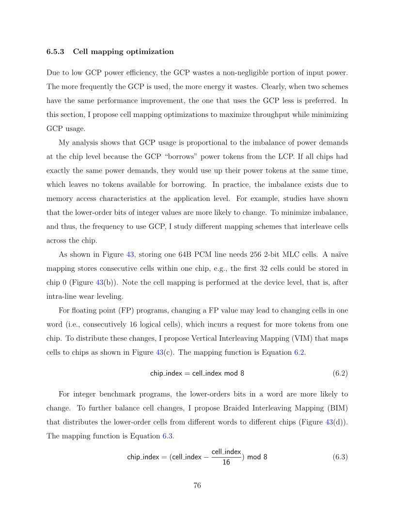
6.5.3 Cell mapping optimization
Due to low GCP power efficiency, the GCP wastes a non-negligible portion of input power.
The more frequently the GCP is used, the more energy it wastes. Clearly, when two schemes
have the same performance improvement, the one that uses the GCP less is preferred. In
this section, I propose cell mapping optimizations to maximize throughput while minimizing
GCP usage.
My analysis shows that GCP usage is proportional to the imbalance of power demands
at the chip level because the GCP “borrows” power tokens from the LCP. If all chips had
exactly the same power demands, they would use up their power tokens at the same time,
which leaves no tokens available for borrowing. In practice, the imbalance exists due to
memory access characteristics at the application level. For example, studies have shown
that the lower-order bits of integer values are more likely to change. To minimize imbalance,
and thus, the frequency to use GCP, I study different mapping schemes that interleave cells
across the chip.
As shown in Figure 43, storing one 64B PCM line needs 256 2-bit MLC cells. A naıve
mapping stores consecutive cells within one chip, e.g., the first 32 cells could be stored in
chip 0 (Figure 43(b)). Note the cell mapping is performed at the device level, that is, after
intra-line wear leveling.
For floating point (FP) programs, changing a FP value may lead to changing cells in one
word (i.e., consecutively 16 logical cells), which incurs a request for more tokens from one
chip. To distribute these changes, I propose Vertical Interleaving Mapping (VIM) that maps
cells to chips as shown in Figure 43(c). The mapping function is Equation 6.2.
chip index = cell index mod 8 (6.2)
For integer benchmark programs, the lower-orders bits in a word are more likely to
change. To further balance cell changes, I propose Braided Interleaving Mapping (BIM)
that distributes the lower-order cells from different words to different chips (Figure 43(d)).
The mapping function is Equation 6.3.
chip index = (cell index− cell index
16) mod 8 (6.3)
76

!"# !$ "$
%
% & ' (
( %
( &
%
&
) "# $)) "$
&
%
(
'
**
+ , - . ,/
,0 ,1 ,2 ,3 .,
.- .. .4 ./ 41
42 43 /+ /, 0.
56 57 5 58 (
% % % % %
% % % % %
& & & & &
& & & & &
( ( ( (
# )
9:; <=>;
?=@ABC
DE FGHIJ
(
% & % (
% & % (
% & % (
% & % (
% & %
KLM
NOP
Figure 43: Different cell mapping schemes.
77

6.6 MLC PCM WRITE POWER MANAGEMENT EXPERIMENTAL
METHODOLOGY
6.6.1 MLC PCM write power management baseline configuration
To evaluate the effectiveness of my proposed schemes, I adopted the same simulation frame-
work from Hay et al. [40] and compared my schemes to existing heuristics. The simulator
is built as a PIN tool, which is used to collect long memory traces. Since my study focuses
on memory subsystem performance and power characteristics, I used a memory trace-driven
simulator (instead of a detailed pipeline simulator) to model accesses to and from MLC PCM
main memory.
My simulator faithfully models the entire memory hierarchy, including L1, L2 and DRAM
last-level caches, the memory controller, and MLC PCM main memory. Several traces
can be combined and interleaved by the simulator to create a multi-programmed workload.
The simulator’s timing model considers cache-to-cache and cache-to-memory bus contention,
bank conflicts, and memory bus scheduling constraints. The memory controller gives higher
priority to read requests. A write request is scheduled only when there is no read request.
When the write queue is full, the memory controller schedules a write burst, which blocks
any pending read requests until all the writes in the queue are finished. This strategy was
also used by Hay et al. [40]. In addition to the normal bus and chip scheduling policies,
writes can only be scheduled when there are enough available power tokens. I also consider
the integration of my schemes with write cancellation and write pausing.
My baseline configuration follows past work [81, 51]. There are eight cores in CMP
system. Each core is single-issue, in-order and can be operated at 4GHz. My trace-driven
simulation methodology limits the simulated cores to be in-order. Each core in the baseline
has a 32MB private write-back DRAM cache to alleviate pressure on MLC PCM main
memory bandwidth. The DRAM cache has a default 256B line size. I also examine 64B and
128B line sizes in a sensitivity study. The detailed parameters can be found in Table 9. The
results showed that my techniques can obtain significant improvement on a wide range of
baseline configurations.
78

Table 9: MLC PCM write power management baseline configuration
CPU 8-core, 4GHz, single-issue, in-orderL1 I/D private, I/D 32KB each/core, 64B line, 2-cycle hit
private, 2MB/core, 4-way LRU, 64B line, write backL2 2-cycle tag, 5-cycle data hit, 16-cycle CPU to L2
DRAM L3 private, offchip, 32MB/core, 8-way LRU, write back256B line, 50ns (200-cycle hit), 64-cycle CPU to L3
Memory onchip, 24-entry R/W queues,Controller MC to bank 64-cycle
4GB, the same line size as L3, single-rank8 banks, MLC read 250ns (1000 cycles)
PCM RESET: 125ns (500 cycles), 300µA, 1.6V, 480µWMain SET: 250ns (1000 cycles), 150µA, 1.2V, 90µW [60]
Memory MLC Write Model: 2-bit MLC[81, 51]‘01’: i/F1/F2 = 2/0.375/0.625, 8 iterations on average;‘10’: i/F1/F2 = 2/0.425/0.675, 6 iterations on average;‘00’: fixed 1 iteration; ‘11’: fixed 2 iterations
I consider a main memory that has a single 4GB MLC PCM DIMM. The 4GB PCM
main memory is divided into 8 banks. A bank spreads across 8 PCM chips. Therefore, 8
banks share 8 PCM chips. A chip’s programming current is supplied by the local charge
pump.
I use the same DIMM power token number PTDIMM as past work [40]. Let ELCP and
EGCP represent the power efficiency of LCP and GCP, respectively. The following formula
computes the maximum power tokens PTLCP that each chip has:
PTLCP = PTDIMM × ELCP ÷ 8 (6.4)
Assume the GCP borrows Borrowedi tokens from each chip (1≤i≤8 and 0≤Borrowedi≤
PTLCP). The following formula computes the power tokens that the GCP can provide:
PTGCP =8∑
i=1
BorrowediELCP
× EGCP (6.5)
Thus, clearly, I have:
PTDIMM =8∑
i=1
PTLCP − BorrowediELCP
+PTGCP
EGCP(6.6)
79

6.6.2 MLC PCM write power management simulated workloads
I modeled a CMP that executes multi-programmed workloads. I chose a subset of programs
from the SPEC2006, BioBench, MiBench and STREAM suites to construct workloads that
exhibit different memory access characteristics. Table 10 lists the R/W-PKI (Read/Write
accesses per thousand instructions) of each workload. I used SimPoint [95] to skip the
warm-up phase. I simulate 1 billions instructions to obtain the performance results.
Table 10: MLC PCM write power management simulated applications
Name Description RPKI WPKI
ast m SPEC-CPU2006 (C), 8 C.astar 2.45 1.12bwa m SPEC-CPU2006 (C), 8 C.bwaves 3.59 1.68lbm m SPEC-CPU2006 (C), 8 C.lbm 3.63 1.82les m SPEC-CPU2006 (C), 8 C.leslie3d 2.59 1.29mcf m SPEC-CPU2006 (C), 8 C.mcf 4.74 2.29xal m SPEC-CPU2006 (C), 8 C.xalancbmk 0.08 0.07
mum m BioBench (B), 8 B.mummer 10.8 4.16tig m BioBench (B), 8 B.tigr 6.94 0.81
qso m MiBench (M), 8 M.qsort 0.51 0.47
cop m STREAM (S), 8 S.copy 0.57 0.42
mix 1 2S.add-2C.lbm-2C.xalan-2B.mummer 1.16 0.58mix 2 2S.scale-2C.mcf-2C.xalan-2C.bwaves 0.94 0.61mix 3 2S.triad-2B.tigr-2C.xalan-2C.leslie3d 0.96 0.58
For my results, I define speedup as:
Speedup =CPIbaselineCPItech
where CPIbaseline and CPItech are the CPIs of the baseline setting and the setting with scheme
tech, respectively. This metric is also used by previous closely related research [81, 51].
Write burst: I adopted a write scheduling strategy from [40]. When write queue is
100% full, a write burst postponing all read requests is issued. And it is finished when the
write queue is drained to be empty. The percentage of time in write burst of our baseline
directly shapes the performance improvement achieved by our schemes. Figure 44 shows
the percentage of write burst in the entire application simulation time for baseline. Since
most of our simulated benchmarks are write intensity, the average percentage of time in
80

write burst for our baseline is 52.2%, which is a strong motivation to improve heavily power
constrained MLC PCM write throughput. Our result on write burst percentage is higher
than that in [40] for several reasons: (i) MLC PCM has ×8 long write latency than SLC
PCM; (ii) compared to the baseline configuration in [40], the CPU frequency in our baseline
is doubled; (iii) larger memory line size and chip level power restriction have more significant
negative influence on write throughput than Flip-n-Write [20].
ast_mbw
a_mlbm_mles_mmc
f_mxal_mmu
m_mtig_
mqso
_mcop
_mmix
_1mix
_2mix
_3gm
ean0.00.20.40.60.81.0
% o
f tim
e in
writ
e bu
rst f
or b
asel
ine
Figure 44: Percentage of execution cycles in write burst for baseline.
6.7 MLC PCM WRITE POWER MANAGEMENT EXPERIMENTAL
RESULTS
I implemented and compared the following schemes.
• Ideal: an ideal scheme that has an unlimited power budget.
• DIMM-only: a scheme that enforces only a DIMM power budget (PTDIMM=560) [40]. The
chip power is unrestricted.
• DIMM+chip: a scheme that enforces both DIMM and chip power budgets using Hay et al.’s
technique [40]. To adopt this scheme, an oracle counter is introduced to provide the exact
number of chip-level cell changes with no latency overhead. Here, PTLCP = PTDIMM ×
0.95 / 8.
• GCP-CL-E: a scheme that uses only FPB-GCP. The cell mapping, CL, may be NE (naıve
mapping), VIM, or BIM. The GCP’s power efficiency, E, ranges from 50% to 95% (0.5
to 0.95).
81

• GCP+IPM: a scheme that uses both FPB-GCP and FPB-IPM. By default, I use GCP-
BIM-0.7 for the GCP. Multi-RESET (MR) is also evaluated.
Evaluation order and normalization. In Figure 35, I showed that the performance
drop from Ideal to DIMM-only is due to iteration-oblivious budgeting, and the drop from
DIMM-only to DIMM+chip is due to the chip power budget. In this section, I aim to restore
these performance drops in reverse order. I first evaluate FPB-GCP with the goal to restore
performance close to DIMM-only. Next, I add FPB-IPM with the goal to restore performance
close to Ideal. In this section, the speedup values are normalized to DIMM+chip.
6.7.1 Effectiveness of FPB-GCP
6.7.1.1 Performance improvement Figure 45 shows IPB-GCP’s effectiveness for dif-
ferent GCP power efficiency values. I used the naıve cell mapping (NE) in this experiment.
I compared GCP with DIMM-only as IPB-GCP aims to eliminate the chip power budget.
ast_mbw
a_mlbm_mles_mmc
f_mxal_mmu
m_mtig_
mqso
_mcop
_mmix
_1mix
_2mix
_3gm
ean1.01.21.41.61.82.0
Speedu
p
DIMM only GCP-NE-0.95 GCP-NE-0.7 GCP-NE-0.5
Figure 45: Speedup with different GCP power efficiencies.
From the figure, the GCP’s power efficiency has a large performance impact. When ELCP
= EGCP, GCP-NE-0.95 is 36.3% better than DIMM+chip. I found that GCP-NE-0.95 and
DIMM-only have the same performance. The reason is, when ELCP = EGCP, there is no waste
to let IPB-GCP borrow tokens from the LCPs (Equation 6.5).
82

In practice, the GCP is likely to be less efficient than the LCP. When EGCP=70% (a
typical value for an off-chip power supply), GCP-NE-0.7 improves performance by 23.7%
over DIMM+chip. However, when the power efficiency is decreased further, its effectiveness
diminishes. When EGCP=50%, the GCP cannot help at all: only 2.8% improvement was
observed.
As the figure shows, some programs are less sensitive to chip power budget. There are
three scenarios. (1) When write operations are intensive, e.g., mcf or mum, the bottleneck
shifts to the DIMM power budget. IPB-GCP often cannot borrow enough tokens to help.
(2) When a program has few writes, e.g., xal, the writes have little performance impact. (3)
When a program has many more reads than writes, e.g., tig, the performance bottleneck
shifts from the writes to the reads such that the chip power budget has a small impact.
6.7.1.2 Cell mapping optimization Figure 46 compares different cell layouts. In these
results, the GCP has practical power efficiency values. When EGCP=70%, VIM and BIM
effectively mask the chip power budget; the performance loss versus DIMM-only is only 2%
and 1.4%, respectively. VIM and BIM are comparably effective with BIM being slightly
better. BIM better balances cells changes when a PCM line stores either FP or integer
values.
ast_mbw
a_mlbm_mles_mmc
f_mxal_mmu
m_mtig_
mqso
_mcop
_mmix
_1mix
_2mix
_3gm
ean1.01.21.41.61.82.0
Speedu
p
GCP-NE-0.7 GCP-VIM-0.7 GCP-VIM-0.5 GCP-BIM-0.7 GCP-BIM-0.5
Figure 46: Speedup of cell mapping optimizations.
More importantly, VIM and BIM allow FPB-GCP to be effective when the GCP’s power
efficiency is 50%. These advanced cell layouts better balance cell changes, which reduces how
often the GCP needs to be employed. With fewer requests sent to the GCP, the advanced
layouts relax the demands on the highly power-inefficient GCP.
83

6.7.1.3 GCP area overhead I next estimated the GCP’s area overhead. Since the area
of the charge pump is proportional to the maximum power that it can provide, I collected
the maximal power tokens requested for GCP under different cell layouts and compared their
area overheads.
ast_mbw
a_mlbm_mles_mmc
f_mxal_mmu
m_mtig_
mqso
_mcop
_mmix
_1mix
_2mix
_3 max
020406080
Max
Tok
en #
NE-0.7 NE-0.5 VIM-0.7 VIM-0.5 BIM-0.7 BIM-0.5
Figure 47: Maximum number of tokens requested by the GCP.
Figure 47 reports the maximum power tokens for each workload when EGCP is 70% and
50%. The maximum requested power tokens are 66, 16, and 28 for the naıve mapping, VIM,
and BIM, respectively. Interestingly, with VIM, the bwa benchmark requires no request to
the GCP, which indicates VIM balanced the cell writes very well across the PCM chips.
Based on the maximum power tokens requested, Table 11 estimates the area overheads
under different schemes. As discussed in Section 6.1, 2xLocal can also mask the chip power
budget. However, this scheme doubles the LCP area on each chip, i.e., 100% overhead. Using
the GCP greatly reduces area overhead. For example, with the VIM cell mapping and 70%
GCP power efficiency, the GCP overhead is only 4.1% of 2xLocal.
I only compare the charge pump size. FPB-GCP also needs a dedicated pin for each PCM
chip to inject the extra power from the GCP. A wire is needed on the DIMM to connect the
GCP to each PCM chip as well. The pin overhead can be justified from the large performance
improvement and small GCP size. For example, a recent design [86] proposed to use extra
pins to inject power for thermal benefits. In addition, FPB-GCP does not modify the DIMM
interface. The changes are localized to the DIMM.
6.7.1.4 Minimize wasted energy When different cell layouts have similar performance
improvements, the mapping that needs fewer power tokens from the GCP is preferred as this
84

Table 11: Charge pump overhead as measured by power tokens
Scheme Power Tokens Overhead
Baseline (8 chips) 70 ∗ 8 = 560 —
2×Local (8 chips) 140 ∗ 8 = 1120 100%
GCP-NE-0.95 66/0.95 = 70 12.5%
GCP-NE-0.70 64/0.70 = 92 16.4%
GCP-VIM-0.95 16/0.95 = 17 3.1%
GCP-VIM-0.70 16/0.70 = 23 4.1%
GCP-BIM-0.95 28/0.95 = 30 5.4%
GCP-BIM-0.70 28/0.7 = 40 7.1%
ast_mbw
a_mlbm_mles_mmc
f_mxal_mmu
m_mtig_
mqso
_mcop
_mmix
_1mix
_2mix
_3 avg0
20406080
Avg
Toke
n #
NE-0.7 NE-0.5 VIM-0.7 VIM-0.5 BIM-0.7 BIM-0.5
Figure 48: Averge power tokens requested by NE, VIM and BIM.
85

helps reduce energy waste on the wire. Figure 48 reports the average number of tokens
requested per line write from the GCP. VIM and BIM greatly reduce the total number of
tokens requested. And thus, on average, VIM and BIM reduce energy waste by 78.5% and
64.4% over the naıve mapping at 70% GCP power efficiency.
6.7.1.5 BIM overall effectiveness The last experiment considers BIM effectiveness
as the GCP’s power efficiency is decreased. Figure 49 reports speedup for three typical
workloads. BIM helps preserve the performance benefit relative to DIMM+chip with very
low GCP power efficiency. For example, in mix 1, BIM is still effective, although GCP power
efficiency is as low as 20%.
0.7 0.6 0.5 0.4 0.3 0.2 0.11.0
1.2
1.4
1.6
Global Charge Pump Efficiency
Speedu
p
astar mcf mix_1
Figure 49: Speedup with BIM as GCP efficiency is decreased.
6.7.2 Effectiveness of FPB-IPM
6.7.2.1 Performance improvement I evaluated the effectiveness of FPB-IPM. The
goal is, together with FPB-GCP, to make performance close to Ideal. Figure 50 reports the
speedup achieved by IPM and Multi-RESET over DIMM+chip. In this figure, GCP is used
with BIM at 70% GCP power efficiency. The figure also reports the geometric mean for
GCP power efficiency values of 50% (gm0.5) and 30% (gm0.3).
On average, IPM improves performance by 26.9% over GCP-BIM. IPM+MR includes
Multi-RESET that splits the first RESET iteration of a write up to 3 new iterations.
IPM+MR has a 30.7% performance improvement over GCP-BIM and 75.6% improvement
over DIMM+chip. This value is within 13.1% of Ideal, which has no power restrictions.
86

ast_mbw
a_mlbm_mles_mmc
f_mxal_mmu
m_mtig_
mqso
_mcop
_mmix
_1mix
_2mix
_3gm
eangm0.5gm
0.31.21.62.02.42.83.2
Speedu
p GCP-BIM IPM IPM+MR Ideal
Figure 50: Speedup achieved by IPM and Multi-RESET.
Also, from the figure, the overall performance improvement decreases with decreasing
GCP power efficiency (compare gmean, gm0.5 and gm0.3). In addition, the improvement
from IPM is stable from 70% GCP efficiency to 50% efficiency but drops at 30%. Multi-
RESET tends to be more beneficial as efficiency decreases. For the benchmarks with a
large number cell changes and a large WPKI, e.g., mcf and mum, IPM achieves significant
improvements over GCP-BIM, indicating IPM makes better use of DIMM power for these
benchmarks.
ast_mbw
a_mlbm_mles_mmc
f_mxal_mmu
m_mtig_
mqso
_mcop
_mmix
_1mix
_2mix
_3gm
ean0.81.21.62.02.42.8
Speedu
p
IPM+MR2 IPM+MR3 IPM+MR4
Figure 51: Multi-RESET iteration split limit.
6.7.2.2 Multi-RESET iteration count Multi-RESET introduces more RESET itera-
tions. In turn, this lowers the maximum power demand but lengthens write latency. I ex-
amined how Multi-RESET should split the RESET iteration; i.e., how many new iterations
should a single RESET be split into. Figure 51 reports performance when Mutli-RESET
87

splits the first RESET iteration up to 2, 3, or 4 new RESET iterations. As shown in the
figure, the best improvement is achieved for 3 iterations. There is a 2% performance decrease
at 4 iterations due to the longer write latency. Thus, I use 3 as the limit when applying
Mutli-RESET.
ast_mbw
a_mlbm_mles_mmc
f_mxal_mmu
m_mtig_
mqso
_mcop
_mmix
_1mix
_2mix
_3gm
ean123456
Nor
mal
ized
Writ
eTh
roug
hput
GCP GCP+IPM GCP+IPM+MR Ideal
Figure 52: Write throughput improvement.
6.7.3 Throughput improvement
As the performance improvement comes mainly from improved write throughput, I report
overall throughput gains in Figure 52. The results are normalized to DIMM+chip. From the
figure, FPB achieves around 58.8% throughput improvement from GCP and 3.4× improve-
ment when both GCP and IPM are applied.
6.7.4 Design space exploration
To evaluate the effectiveness of my proposed fine-grained power budgeting schemes under
different settings, I did experiments in a wide design space with different memory line sizes,
last-level cache capacities, number of entries in the write queue, and number of power tokens.
I also integrated my FPB schemes with the state-of-the-art designs for MLC PCM — write
cancellation, write pausing [81] and write truncation [51]. These methods are orthogonal
to power budgeting. In the design exploration, I use IPM+MR with BIM and EGCP=70%. I
abbreviated this combined scheme as FPB.
In the comparison, when studying the sensitivity of parameter X, each bar is normalized
to DIMM+chip having the same X value. But different bars have different X values.
88
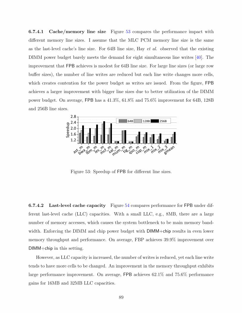
6.7.4.1 Cache/memory line size Figure 53 compares the performance impact with
different memory line sizes. I assume that the MLC PCM memory line size is the same
as the last-level cache’s line size. For 64B line size, Hay et al. observed that the existing
DIMM power budget barely meets the demand for eight simultaneous line writes [40]. The
improvement that FPB achieves is modest for 64B line size. For large line sizes (or large row
buffer sizes), the number of line writes are reduced but each line write changes more cells,
which creates contention for the power budget as writes are issued. From the figure, FPB
achieves a larger improvement with bigger line sizes due to better utilization of the DIMM
power budget. On average, FPB has a 41.3%, 61.8% and 75.6% improvement for 64B, 128B
and 256B line sizes.
ast_mbw
a_mlbm_mles_mmc
f_mxal_mmu
m_mtig_
mqso
_mcop
_mmix
_1mix
_2mix
_3gm
ean
1.21.62.02.42.8
Speedu
p 64B 128B 256B
Figure 53: Speedup of FPB for different line sizes.
6.7.4.2 Last-level cache capacity Figure 54 compares performance for FPB under dif-
ferent last-level cache (LLC) capacities. With a small LLC, e.g., 8MB, there are a large
number of memory accesses, which causes the system bottleneck to be main memory band-
width. Enforcing the DIMM and chip power budget with DIMM+chip results in even lower
memory throughput and performance. On average, FBP achieves 39.9% improvement over
DIMM+chip in this setting.
However, as LLC capacity is increased, the number of writes is reduced, yet each line write
tends to have more cells to be changed. An improvement in the memory throughput exhibits
large performance improvement. On average, FPB achieves 62.1% and 75.6% performance
gains for 16MB and 32MB LLC capacities.
89

ast_mbw
a_mlbm_mles_mmc
f_mxal_mmu
m_mtig_
mqso
_mcop
_mmix
_1mix
_2mix
_3gm
ean0.81.21.62.02.42.8
Speedu
p
8M 16M 32M 128M
Figure 54: Speedup of FPB for different LLC capacities.
6.7.4.3 Number of write queue entries Figure 55 shows FPB’s effectiveness for dif-
ferent numbers of entries in the write queue. The writes in the queue are flushed when the
queue is full. With more entries in the queue, the bursty flush tends to request more power
tokens, which is sensitive to write throughput. On average, FPB improves performance by
75.6%, 85.2% and 88.1% for three write queues.
ast_mbw
a_mlbm_mles_mmc
f_mxal_mmu
m_mtig_
mqso
_mcop
_mmix
_1mix
_2mix
_3gm
ean1.21.62.02.42.83.2
Speedu
p 24 48 96
Figure 55: Speedup of FPB for different write queue sizes.
For benchmarks with large WPKI, such as mum, FPB has a large speedup. The overall
performance improves significantly when increasing the entry count from 24 to 48, and
saturates at 48 — 96-entry write queue does not exhibit notable improvement over 48-entry
queue.
90
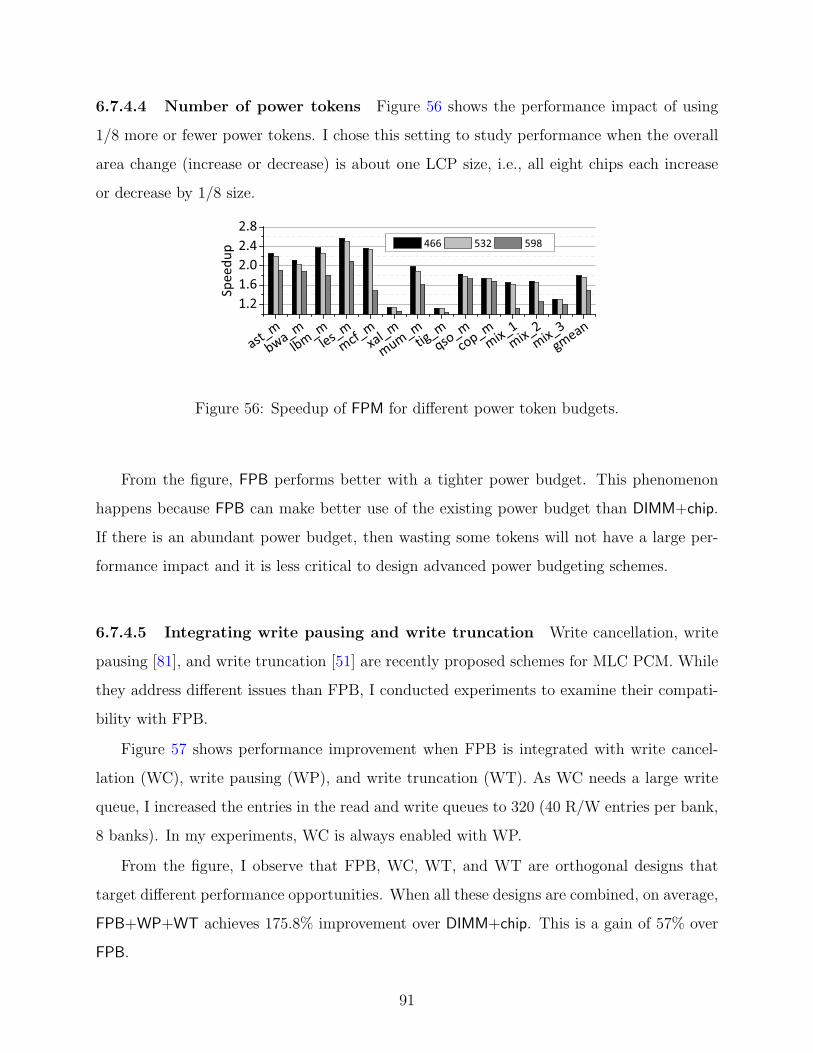
6.7.4.4 Number of power tokens Figure 56 shows the performance impact of using
1/8 more or fewer power tokens. I chose this setting to study performance when the overall
area change (increase or decrease) is about one LCP size, i.e., all eight chips each increase
or decrease by 1/8 size.
ast_mbw
a_mlbm_mles_mmc
f_mxal_mmu
m_mtig_
mqso
_mcop
_mmix
_1mix
_2mix
_3gm
ean
1.21.62.02.42.8
Speedu
p 466 532 598
Figure 56: Speedup of FPM for different power token budgets.
From the figure, FPB performs better with a tighter power budget. This phenomenon
happens because FPB can make better use of the existing power budget than DIMM+chip.
If there is an abundant power budget, then wasting some tokens will not have a large per-
formance impact and it is less critical to design advanced power budgeting schemes.
6.7.4.5 Integrating write pausing and write truncation Write cancellation, write
pausing [81], and write truncation [51] are recently proposed schemes for MLC PCM. While
they address different issues than FPB, I conducted experiments to examine their compati-
bility with FPB.
Figure 57 shows performance improvement when FPB is integrated with write cancel-
lation (WC), write pausing (WP), and write truncation (WT). As WC needs a large write
queue, I increased the entries in the read and write queues to 320 (40 R/W entries per bank,
8 banks). In my experiments, WC is always enabled with WP.
From the figure, I observe that FPB, WC, WT, and WT are orthogonal designs that
target different performance opportunities. When all these designs are combined, on average,
FPB+WP+WT achieves 175.8% improvement over DIMM+chip. This is a gain of 57% over
FPB.
91

ast_mbw
a_mlbm_mles_mmc
f_mxal_mmu
m_mtig_
mqso
_mcop
_mmix
_1mix
_2mix
_3gm
ean
1.6
2.4
3.2
4.0
Speedu
p
FPB FPB+WC FPB+WC+WP FPB+WC+WP+WT
Figure 57: FPB with WC, WP and WT.
However, FPB+WP+WT has a smaller improvement over WP+WT. This result happens
because WC, WP and WT mitigate the importance of writes on performance — i.e., WC and
WP move many writes off the critical path and WT reduces write latency. As discussed, FPB
gains performance due to improved write throughput. Thus, when writes are less critical,
the performance improvement from FPB is less.
92

7.0 PCM PEAK POWER REDUCTION
7.1 BACKGROUND
7.1.1 High density PCM
High density PCM can be achieved through using smaller access device (Figure 59(a)) with
a compact structure because the area of the access device dominates the size of a cell.
Three types of access devices have been implemented in PCM prototypes: MOS [55], bipolar
junction transistor (BJT) [8] and diode [61]. They, in that order, create decreasing PCM cell
sizes, as shown in Figure 58(a). As a result, a PCM bank built with MOS access device will
be larger than with BJT. And a diode-switched PCM array will be the smallest. A diode-
switched PCM achieves a minimum of 4F 2 cell size. The cell has a vertical structure including
a bit-line, a top electrode contact, a phase-change material such as GST, a self-aligned bottom
electrode contact and a diode [61]. I modeled a 1GB PCM following a prototype [22] with
those three different access devices, and measured their area using NVsim [28]. The results,
shown in Figure 58(b), are all normalized to the area of the MOS-switched PCM array.
The BJT-switched PCM array is only 63% of the MOS-switched array in area. The diode-
switched array further reduces it to 44%. A multi-level cell (MLC) with a diode (MLC-Dio)
achieves the minimum area: only 26% of the original area is required. Due to such great
density advantage, many recent PCM prototypes and products adopt diode-switched PCM
cell design in 58nm [23] (2011) and 20nm [22] (2012).
However, a diode has the highest Vth among the three access devices [61], as also shown in
Figure 58(a). Additionally, diode-switched PCM has larger parasitic resistance on its bit-line
in high-density PCM array architecture [22]. Hence, it needs higher read and write voltages
93

MOS BTJ Diode0.81.01.21.41.61.82.02.2
Vth Cell SizeVt
h(V)
24681012141618
(b) 1GB chip area
Cell Size(F2)
(a) Vth
and cell sizeMOS BTJ DiodeMLC-Dio
0.00.20.40.60.81.0
Norm
alize
d Ar
ea CP Array
Figure 58: Trade-off between Vth and chip density.
than MOS- and BJT-switched PCM, which means that larger CPs for reads and writes are
necessary to overcome the Vth and parasitic resistance. The area of the corresponding CP
for three different devices are also shown in Figure 58(b). Regardless of the reduction of the
entire chip area, the area of CP enlarges more than two times from MOS-, to diode-switched
arrays. CP occupies 43% of the array area in MLC-Dio. As will be introduced later, on-chip
CP has low conversion efficiency (only ∼20%). When the area proportion of CP grows, more
leakage power is dissipated and higher power attrition there is. This is the problem I will
address in this work.
7.1.2 Multi-level cell (MLC) PCM
Time
(b) Asymmetric write (c) Iteration‐based write
Po
we
r
Reset
Set1Verify
...
Set0Verify
RESET
SET
TresetTset
Time
Cell
B/L
W/L
(a) Cell
Access
Device
Figure 59: PCM basics.
94

The phase change material used in PCM, such as GST, has two stable states — full
crystalline and full amorphous states. The resistance difference between these two states
is often more than 10000× apart [89]. Multi-level cells (MLC) can thus be implemented
through creating multiple intermediate states to represent more binary bits, e.g. four states
for two bits. The intermediate states are partial crystalline and partial amorphous material
states.
There are two PCM write operations — RESET and SET. The RESET is performed
by applying a large but short pulse to the GST material and convert it from crystalline to
amorphous state. The SET is performed by applying a smaller but longer pulse for the reverse
state transition, as illustrated in Figure 59(b). Such an asymmetric write characteristic
indicates that the PCM power consumption is largely determined by the RESET operation.
Its high pulse also requires a significantly larger CP than the SET and read operation does.
Programming an MLC requires multiple steps to reach a target resistance level due to
significant write non-determinism caused by process variations and material composition
fluctuation [9, 67]. Also, a cell value is represented by a resistance range rather than a
specific point. An iteration-based write scheme is adopted to program a cell into a target
resistance range, as illustrated in Figure 59(c). This is the widely used Program-and-Verify
(P&V) scheme [69, 74] that first applies a RESET pulse to place cells that need to be changed
into similar initial states, and then applies a number of SET pulses, verified by reads in each
iteration, to ensure the write accuracy.
Recent studies revealed that writing different cell values requires different numbers of
iterations [81, 51]. In 2-bit MLC, for example, writing 00 can finish immediately after the
RESET iteration. Writing 01 or 10 requires more iterations than writing 00 or 11. It is this
property that I will leverage to develop a scheduling scheme to lower the peak power during
a write. Also, based on the cell values to be written, a PCM line write may require different
numbers of iterations at different times. I will adopt the same scheme in this paper. Detailed
parameters are reported in Section 7.4.
95

7.1.3 The baseline memory architecture
The baseline memory architecture (as shown in Figure 36) is derived from a previous MLC
PCM model [48] and a new memory interface LPDDR2-NVM (Low Power DDR2 for Non-
Volatile Memory) [22]. Previous work [48] adopted eight 8-bit PCM chips to constitute eight
banks on one DDR2 DIMM. LPDDR2-NVM interface only supports 8, 16 and 32-bit wide
chips. In this paper, I set chip width as 16-bit. Hence, there are now four chips per rank, and
each logic bank spreads across four chips. The channel adopts the dual line package (DLP)
architecture [65], which has single LPDDR2-NVM package on both sides of the board. One
LPDDR2-NVM package has four 1GB chips, as with the prototype demonstrated in [22]. It
was also demonstrated that one chip can support 128 parallel RESETs independently. In
this paper, I assume one MLC PCM chip can support 140 concurrent writes, similar to that
in [48]. I will prove that I can reduce this need by 70%.
Due to non-deterministic MLC PCM write, a bridge chip is integrated on-DIMM to
regulate the P&V iteration levels [31]. Regulating MLC write by the bridge chip instead
of the memory controller minimizes sub-optimal utilization of the memory bus. Finally, a
large DRAM cache for the PCM memory is assumed, which can buffer write-intensive lines
to benefit PCM in both endurance and power.
I also adopt two levels of CP design as proposed in [48]: local CP (LCP) and global
CP (GCP). The latter was introduced to distribute power according to the need of each
individual chip. In summary, I adopt a state-of-the-art baseline where CPs are designed to
ensure that power is most efficiently used.
7.2 CHARGE PUMP BASICS AND MODELING
Recent advances in PCM incorporate both on-chip and off-chip power supplies [66, 22, 55,
61]. Even though external power supply was available, on-chip CPs still predominate, as
demonstrated in [22]. This is because 1) PCM requires multiple boosted voltages in different
components of a chip, and hence, single external power rail is insufficient to achieve that;
96

2) the write voltages need fine-grained control for pulse shaping, location compensation
etc. circuit-level requirements, which cannot be achieved via external power; and 3) fully
depending on external power supply is not a portable solution because different vendors may
require different voltage boost levels. Hence, I focus on optimizing on-chip CMOS-compatible
CPs and present first the models used in this paper.
7.2.1 CMOS-compatible on-chip charge pumps
A CP converts the supply voltage Vdd to a DC output voltage Vout higher than Vdd. CMOS-
compatible CP consists only of capacitors and switches, so it can be integrated on-chip easily.
A CP has several stages, each elevating the voltage a little, as shown in Figure 60(a). Adding
more stages can raise the output voltage to a target level that is multiple times higher than
Vdd [73].
There are two types of CPs [73]: one with purely capacitive load and the other with a
current load. The former does not need to supply any current and only provides a target
output voltage, which can be applied on X/Y decoders to reduce the parasitic resistances of
the transistor switches along the read/write current path [55, 22]. It has a negligible area
overhead and almost perfect power conversion efficiency, e.g. 95% [39]. The latter supplies
both a target output voltage and a large amplitude of current, which are essential for READ,
RESET and SET operations. It incurs large die area overhead and has low power conversion
efficiency, e.g. 20% [61]. Figure 60(c) shows a CP system [61] for a diode-switched PCM
chip using both types of CP. The capacitive load pumps are used for X/Y decoders. The
READ, SET, and RESET operations require voltages of 3.0V, 3.0V and 5.0V respectively,
in contrast to a 1.8V Vdd. They require current load pumps which have low efficiency and
large die area overhead.
When there is a need for more output current, e.g., writing multiple MLC cells, either a
larger CP is needed and/or more modular pump units are needed such that the aggregated
current matches the demand for writing multiple cells. In this paper, I choose to integrate
modular CP units for their flexibility in adjusting voltage output, as with recent chip de-
mos [61]. The organization of a write CP can be viewed in Figure 60(b). When different
97

(a) A N‐stage CP unit
Vdd C
Vck
S0C
Vck
S1CL
SN
...
C
Vck
IL
(c) A CP system for a PCM array(b) A multi‐unit CP system
Ctrl
Unit
Discharge Unit
En0
En1
EnN
Pump Unit0
Pump Unit1
Pump UnitN
...
Pump Driver0
Pump Driver1...
Pump DriverN
Vout+IL0
Vout+IL1
Vout+ILN
Vdd
Yd
ec
Write Driver
S/A Unit
X d
ec
Y Selector
X Selector
PCM
ArrayDEC. CP
READ CP
RESET CP
SET CP
Figure 60: Charge pump basics.
number of pump units are enabled (by the Eni signal), the circuit can support ×2, ×4, ×8
and ×16 concurrent cell writes. In [61], one pump unit can RESET two cells. I share the
same assumption in this paper. Finally, a discharge unit is also necessary. It is responsible
for discharging pump units to Vdd. The discharge process is an atomic operation that cannot
be interrupted.
7.2.2 Charge pump modeling
A CP with a current load is both a power supplier and consumer. Besides the power delivered
to the output network, part of the input power is consumed on parasitic effect, and part of
the input is leaked away. Also, the peripheral circuits that support the CP core circuits drain
considerable power. The parasitic power is the power consumed on charging/discharging
the internal parasitic capacitance that do not contribute to the output [73, 107], and is
proportional to the capacitance of internal pumping capacitors [73]. The parasitic power is a
dominant factor in the wasted power of a CP since the internal capacitors are very large [73].
The leakage power is the power leaked from supply to ground [107]. Leakage is also quite
large as a result of very strong transistors and high voltages on output and internal nodes.
The peripheral power is the power consumed on supportive circuits such as controls, drivers,
clock distribution etc.
I follow the latest previous work [73] on CP modeling. Since the model does not consider
transistor leakage, I also built CPs for different operations in HSPICE and measured the
leakage power which is then integrated into the analytical CP model. The HSPICE imple-
98

mentation with design parameters was also used to verify critical metrics against the model.
The critical metrics are area, wasted power, charge and discharge latency, and charge en-
ergy. All metrics are functions of N, the number of stages used in a pump unit (Figure 60
(a)). I will summarize their analytic models respectively and then provide a design space
exploration on those metrics for an optimal selection of N.
Total current supply. The total current is modeled as follows:
TC =
[(N+ 1) + α · N2
(N+ 1) · Vdd − Vout· Vdd
]· IL (7.1)
where, α is the constant proportional factor between the bottom plate parasitic capacitance
and the pumping capacitance. IL is the load current, which is all the current that drains
from the CP output that can cause the attenuation of CP output voltage. IL mainly consists of
three components: 1) the dynamic current used by the load, i.e. read/write current applied
to PCM cells, denoted as IL−dynamic. This is the current for doing useful work. 2) the leakage
of the load, denoted as IL−output−leak; and 3) the leakage of the CP itself, denoted as IL−CP−leak.
Hence,
IL = IL−dynamic + IL−output−leak + IL−CP−leak (7.2)
Wasted power. The wasted power is calculated as:
WP = TC× Vdd − Vout × IL−dynamic (7.3)
which includes parasitic power and the leakage power from both the output load and the
internal CP circuit.
Area. The die area of a CP is proportional to the maximum current it can provide [73]:
Atot = k · N2
(N+ 1) · Vdd − Vout
ILf
(7.4)
where Atot is the total area of the CP, k is a constant that depends on the process used
to implement the capacitors, f denotes the working frequency of the CP, Vdd is the supply
voltage, Vout is the target programming voltage, and N is the number of stages in a pump
unit as shown in Figure 60 (a).
Charge/Discharge latency. The charge and discharge latencies indicate the time
spent to raise the output voltage to the target voltage level, and from the target voltage to
99

Vdd, respectively. For the same CP configuration, the higher the output voltage is, the longer
time the CP spends in charging/discharging.The charge latency, tr, is calculated as:
tr = T · N2 · ( CL
CTot+
1
3) · ln(N+ 1− vx0
N+ 1− vx) (7.5)
where T is 1f, the period of a CP. CL represents the total capacitance load. CTot means the
total pumping capacitance. vx0 is initial voltage and vx is target voltage.
Charge energy. The charge energy is the energy consumed during CP rise time. And
it is defined as:
Q(tr) = (N+ 1)(1
3CTot + CL)(vx − vx0) + αCTotVdd
trT
(7.6)
With all parameters considered, the model details of CPs are summarized in Table 14 in
Section 7.5.
From equation (7.3)-(7.6), I can see that all essential metrics are functions of N. To
achieve an optimized design, I performed a design space exploration on N. Figure 61 exhibits
the results for RESET and READ CP in my baseline. The SET CP design follows the READ
CP as they have the same output voltage. I normalize all values to the minimal value of the
corresponding metric for ease of comparison. For the RESET operation, I select N=3 as the
stage number for the RESET CP for its low overhead in all metrics including wasted power
(Wasted), charging latency (Tcharge) and energy (Echarge). This setting will be used in my
baseline design, which will be compared against my proposed technique that uses a hybrid
design with two different stage numbers for overall power and energy savings. For the READ
CP, all smallest overhead and performance metrics are obtained when N=1. Hence, I adopt
a single stage CP design for both READ and SET operations.
Verification and Leakage Power. I implemented an actual CP design [73, 107] in
HSPICE with target requirements and the optimal stage number obtained above, to verify
the metrics against the model. The CPs are implemented using high voltage transistors and
MOS-capacitors. I measured the leakage power and summarized them in Table 12. The
leakage power of each specific CP is proportional to its area and stage number, since more
stages incur larger number of transistors. Compared to HSPICE simulation results, the
metrics calculated from equation (7.3)-(7.6) have less than 10% deviation. I used values
obtained from the model in my designs and evaluations.
100

1 2 3 4 5 6 7 8 9 1001234
0 1 2 3 4 5 6 7 8 9 10012345
Area Wasted Tcharge Echarge
Norm
alize
d to
min
RESET CP stage num Norm
alize
d to
min
READ CP stage num
Figure 61: The RESET and READ CP modeling.
Table 12: Leakage power for all types of CPs.
CP Type RESET SET READLeakage Power (mW ) 2.0 0.42 0.51
7.3 PROPOSED DESIGNS
7.3.1 Motivation
Besides the wasted power dissipated in CPs, the memory interface, peripheral circuit of the
data arrays also dissipate significant leakage power. Previous work proposed to power gate
peripheral circuits upon completion of an operation with small performance penalty [116].
As I will show next that the wasted power in CP predominates the leakage dissipated in
the peripheral circuits of data arrays, especially when large CPs are used for high-voltage
operations such as RESET.
RESET CP SET CPREAD CP Other
0200400600800
100012001400
Pow
er (m
W) Parasitic
Dynamic Leakage
Figure 62: Power breakdown.
101

Figure 62 shows a power breakdown of a diode-switched PCM chip (22nm 8GB 2-bit
MLC) in my baseline. I show both dynamic and wasted power (mainly parasitic and leakage
power) for the RESET CP, SET CP, READ CP, and all remainder components (Other) in-
cluding the data bank itself, peripheral circuits and the LPDDR2 interface. The CP for X/Y
decoders has only capacitive load and hence dissipate negligible power, compared to other
components. To obtain those results, I model the PCM chip architecture following mainly a
recent prototype [22]. The bank itself is modeled using NVsim [28]. The LPDDR2 modeling
is based on [66, 65]. More experimental parameters can be found in Section 7.4.
It is clear from the results that the bulk of power dissipation goes to all CPs, especially
the RESET CP, due to their large target output voltages, but low power conversion efficiency.
The Vdd of the PCM bank is 1.8V [22], and the LPDDR2 interface is 1.2V Vdd [65], but the
working voltage for READ, SET and RESET are 3.0V, 3.0V and 5.0V respectively. Also,
only around 20% of conversion efficiency (Dynamic power / (Dynamic power + Wasted
power) ≈ 20%) was observed for RESET CP, similar to that reported in [61]. As a result,
most of the power is wasted on CPs, and the larger the CPs the more waste power there is.
Moreover, the total power dissipated by RESET CPs is more than 50% of the total PCM
chip power. This is not only because the RESET by itself has the highest power requirement,
but also because its CP is designed to accommodate the worst case scenario where there are
multiple concurrent RESETs. More pump units are required to satisfy such peak power
demand, and hence, larger area are required and more power waste is generated. If the peak
power demand is reduced, I can then use smaller CPs to achieve both area and wasted power
reduction. This is one objective of my design in this work.
7.3.2 Intra-write RESET Scheduling (Reset Sch)
The P&V programming strategy for writing an MLC PCM line starts with a RESET itera-
tion, followed by a non-deterministic number of SET iterations. In particular, the number of
SET iterations is cell value dependent [51]. I use a 2-bit MLC as an example for illustration
in this paper. On average, writing value “01” requires more iterations than writing “10”
and “11”, while writing “00” can finish immediately after the RESET iteration. A RESET
102
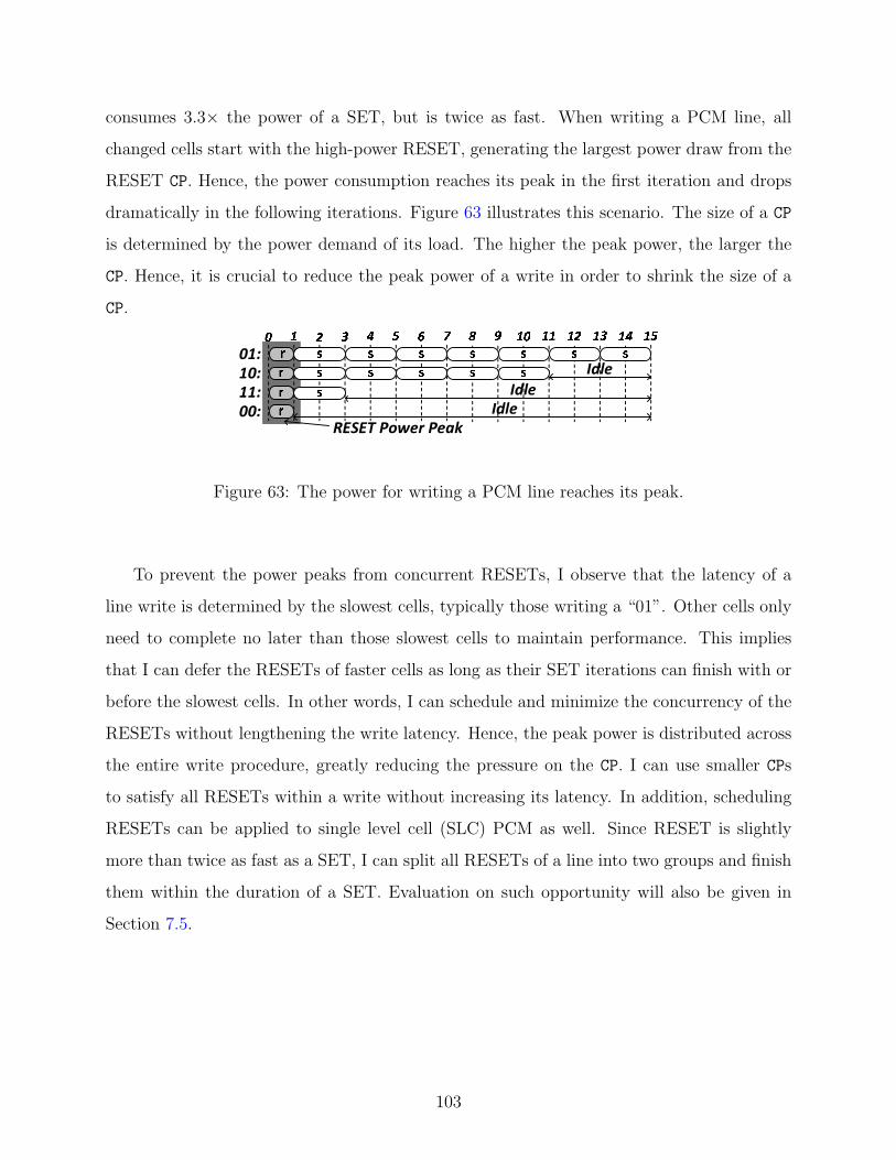
consumes 3.3× the power of a SET, but is twice as fast. When writing a PCM line, all
changed cells start with the high-power RESET, generating the largest power draw from the
RESET CP. Hence, the power consumption reaches its peak in the first iteration and drops
dramatically in the following iterations. Figure 63 illustrates this scenario. The size of a CP
is determined by the power demand of its load. The higher the peak power, the larger the
CP. Hence, it is crucial to reduce the peak power of a write in order to shrink the size of a
CP.
01:
10:
11:
00:
RESET Power Peak
Idle
Idle
Idle
Figure 63: The power for writing a PCM line reaches its peak.
To prevent the power peaks from concurrent RESETs, I observe that the latency of a
line write is determined by the slowest cells, typically those writing a “01”. Other cells only
need to complete no later than those slowest cells to maintain performance. This implies
that I can defer the RESETs of faster cells as long as their SET iterations can finish with or
before the slowest cells. In other words, I can schedule and minimize the concurrency of the
RESETs without lengthening the write latency. Hence, the peak power is distributed across
the entire write procedure, greatly reducing the pressure on the CP. I can use smaller CPs
to satisfy all RESETs within a write without increasing its latency. In addition, scheduling
RESETs can be applied to single level cell (SLC) PCM as well. Since RESET is slightly
more than twice as fast as a SET, I can split all RESETs of a line into two groups and finish
them within the duration of a SET. Evaluation on such opportunity will also be given in
Section 7.5.
103

However, exceptions can occur since MLC PCMwrite exhibits significant non-determinism
[9, 67], and writing a “10” may be slower than writing a “01” occasionally, which prolongs
the write latency if the RESET of the former is delayed. Nevertheless, scheduling RESETs
according to the average number of SET iterations for different cell values imposes negligible
impact on write latency, as will be shown in my experiments.
s s s ss s
S‐slack
01:
10:
11:
00:
s
s s s s sr
r
r
r
s
0 1 2 3 4 5 6 7 8 9 10 11 12 13 14 15
S‐slack
S‐slack
Figure 64: Scheduling RESETs without harming write latency.
The RESET scheduling (Reset Sch) mechanism I propose is a simple heuristic based
on the average number of SET iterations for writing four different values, as depicted in
Figure 64. Let S-slack denote the time slot interval in which a RESET iteration can be
scheduled without prolonging the write latency, assuming there is always a cell needed to
be changed to “01”. Hence, the S-slack for writing “10” is 4, “11” is 12 and “00” is 14,
as depicted in Figure 64. Note that the S-slack for “00” is aligned with “11” in the figure
because 1. it simplifies the scheme; 2. it does not bring much benefit otherwise, according
to my experiments; and 3. occasionally a line may take less time than predicted so that
finishing “00” sooner actually benefits. The scheduling works as the following:
• For “01” cells, I do not defer their RESETs.
• For “10” cells, I defer their RESETs until after all RESETs for 1. have finished, but
before the end of their S-slack, which is 4 in Figure 64.
• For “11” and “00”cells, I defer their RESETs until after all RESETs for 2. have finished,
but before time slot 12 in Figure 64.
In all above cases (and baseline design as well), the concurrency degree of RESETs is bounded
by the capacity of the RESET CP. For example, if the RESET CP can support R RESETs
per time slot but there are more than R RESETs, I then spill the extra RESETs to the next
time slot, and so on. In some extreme cases, such spilling could go beyond the S-slack,
104

postponing all subsequent cell writes and prolonging latency of writing the entire line. Such
scenario can be mitigated through value encoding (as described below), and proper selection
of R, as will be demonstrated in my evaluation results.
Value encoding. My Reset Sch favors to write “11” and “00” as they have larger
S-slacks than “10” and “01”. I adopt a recently proposed data value mapping scheme [101]
to create more “11” and “00” for a memory line. This encoding scheme divides cell values
into two categories: “11”/“00”, and “01”/“10”, and dynamically remaps values to ensure a
line contains more cells in the first category. Since the cells in the first category consumes
less per-cell write energy, the new mapping reduces dynamic write energy of MLC PCM. I
further extend this encoding by flipping the bits if there are more “01” than “10” in a line.
The hardware overhead involves only a two-bit MLC call tag per line. A read operation,
before returning the line, interprets this tag and restore the original values if necessary. The
hardware cost is trivial as in [101]. When combined with differential write [116, 60], the
remapping is disabled if there are more cell changes, the same as that in [101].
Comparing to prior art. The schemes that are close to Reset Sch include Toff schedul-
ing [43] and Multi-RESET [48]. Both manage SET and RESET iterations within one line
write.
• Toff scheduling. For P&V MLC programming, a cell being changed needs a delay to
stabilize resistance drift and recover Vth between each SET and read/verify pair. This
delay is referred as Toff in [43]. A Toff skew write scheme was proposed to interleave SETs
from multiple cells, which maximizes SET throughput of MLC PCM without increasing
SET current or SET pump size. This scheme has no impact on RESET pump size
because RESET operation does not have Toff , and scheduling SETs does not conflict
with scheduling RESET.
• Multi-RESET. To enable more MLC line writes with fixed input power budget, the multi-
RESET scheme proposed in [48] divides all RESETs into several groups and each group
can be performed with currently available power budget. Multi-RESET, while starting
MLC write early, prolongs the latency of this particular MLC line write. Therefore,
performing multi-RESET too aggressively would harm system performance [48]. I will
compare Reset Sch with multi-RESET in the experiments.
105

7.4 PCM PEAK POWER REDUCTION EXPERIMENTAL
METHODOLOGY
Simulator: I evaluated my proposed designs using a PIN-based simulator Sniper [15]. I
modified the simulator to model all memory hierarchies, power budgeting constraints [48],
and CP system.
Baseline Configuration: The detailed baseline parameters can be found in Table 13.
Unless otherwise stated, I adopt diode-switch MLC PCM based main memory system. Other
types of PCM main memory results are also reported.
Table 13: PCM peak power reduction baseline configuration
CPU four 4GHz, X86 out-of-order cores, 4-wide issue,8MSHRs/core, 128-entry instruction window
L1 I/D private, I/D 32KB each/core, 4-way, LRU, 64B line, 2-cycle hitL2 private, 2MB/core, 8-way, LRU, 64B line, write back,
2-cycle tag, 5-cycle data hit, 16-cycle CPU to L2DRAM L3 private, offchip, 32MB/core, 16-way, LRU, write back,
64B line, 50ns (200-cycle hit), 64-cycle CPU to L3Memory onchip, 24-entry R/W queues, MC to bank 64-cycle,
scheduling reads first, issuing writes when there is NO read,Controller when W queue is full, issuing write burst (only scheduling
writes and delaying reads, when W queue is empty)Main Memory 16GB, 64B line, 2 channels, 1 channel per DIMM, 2 ranks per
channel, 4 banks per rank, 64-bit channel width
Table 14: 2-bit MLC PCM chip and main memory configuration
Memory 22nm PCM process, LPDDR2-NVM interface, I/O bandwidth: 800Mb/s/pin,4 chips per rank, 4 banks interleaved on 4 chips
Chip 4 F 2 cell, diode-switch, 16-bit width, 1GB, 1.8V vdd, 133MHz,140 concurrent RESETs power budget
CP per 133MHz, RESET/SET/READ CP: 5/3/3V target voltage, 7/3.5/4.3mA loadChip current, 21.6%/30.9%/30.9% power efficiency
159/132/132ns charge latency, 100/87.5/87.5ns discharge latency,charge energy 18.78/2.76/3.31/2.86(FAST RD)nJ
Read 3V, 8.4µA, 5.6nJ per line, critical word 125ns, MLC read 250nsWrite RESET: 5V, 100µA, 29.7pJ per bit, 50ns operation latency,
125ns iteration latency; SET: 3V, 50µA, 22.5pJ per bit150ns operation latency, 250ns iteration latency(including Toff [43]& verify), MLC Write Model: 2-bit MLC [81, 51]
106

Chip Modeling: I used NVsim [28], a CACTI-based non-volatile memory modeling
tool, to calculate my 22nm diode-switch PCM chip parameters. The chip modeling is based
on the latest industrial prototype [22]. I modeled CP as discussed in Section 7.2.2, fitting con-
stants in [73] and related parameters in [22, 61]. I calculated read and write latency/energy
by feeding the parameters from [22, 61] to NVsim. I used the same non-deterministic write
model as previous work [81, 48]. The detailed memory, chip, CP, read and write parameters
can be found in Table 14.
Simulated Workloads: I choose a subset of programs from SPEC2006, BioBench, and
STREAM suites to construct multi-programmed workloads covering different memory access
characteristics. The workload mix 1 consists of astar, bwaves, gemsFDTD and leslie3d, and
mix 2 consists of astar, bwaves, milc and mummer.
7.5 RESULTS AND ANALYSIS
7.5.1 Reset Sch: Power Reduction and Performance
I will present first how much area reduction for RESET CPs is achieved, and then show the
impact of such reduction on performance. The wasted power reduction is proportional to
the area reduction. Since I adopt a modular CP design, its area is thus linear to the number
of modular pump units which decides the peak power provisioning to the memory, or how
many RESETs can concurrently occur. This is the capacity of the RESET CP, and a critical
parameter in my design. A small capacity implies small CP size but spilling of RESETs to the
next iteration may occur in each step of the scheduling, creating performance degradation.
A generous capacity implies large CP size, but more RESETs can be packed in each iteration
and writing a line can finish sooner. My objective is to identify the smallest RESET CP that
does not bring performance overhead. I compare the following three choices of the capacity
with the baseline.
• Base: My baseline implements the state-of-the-art fine-grained power budgeting tech-
nique including the multi-RESET scheme [48], which makes the best use of available
107

power for higher performance. All RESET CPs are on in Base with power gating on
arrays during idle period [116].
• SumofMax: This builds Reset Sch on top of Base. The capacity of the RESET CP supports
(max01+max10) number of concurrent RESETs, where maxxx is the maximal number of
xx occurrence in writing a single line throughout the simulation duration. This scheme
guarantees that writes are not prolonged since there is enough power to write 01 and 10
at the same time.
• Max01: The capacity is now reduced to max01, presuming max01 > max10 as writing 01
is the longest operation.
• MinofMax: The capacity is reduced further to min(max01,max10). This scheme utilizes
my enhanced version of value encoding to reduce max01 through bit flipping if there are
more 01 then 10 in a line.
Figure 65 reports the required sizes of the RESET CP for three different capacities,
normalized to the Base. This figure also reflects achieved wasted power reduction for RESET
CPs. The results show that SumofMax only requires 70% of the RESET CPs in Base. Max01
and MinofMax can further shrink the sizes down to 38% and 33% of the RESET CPs in Base.
As I can see, opportunities in reducing the wasted power and area of a RESET CP through
Reset Sch is substantial. This does not have to be done at the cost of performance, as I
show next.
ast_mbwa
_mgem
_mlbm_mles_mmil_mzeu_
mmum_mtig_mstr_m mix1 mix2
gmean0.20.40.60.81.0
RESE
T CP
size
Norm
alize
d
SumofMax Max01 MinofMax
Figure 65: The potential of CP size reduction and wasted power reduction.
Figure 66 compares the performance of SumofMax, MinofMax and MinofMax-30% (ex-
plained later), all normalized to the Base. It is interesting to observe that SumofMax and
MinofMax improvement performance over Base by 2.6% and 2.1% respectively. The reason
108

ast_mbwa
_mgem
_mlbm_mles_mmil_mzeu_
mmum_mtig_mstr_m mix1 mix2
gmean0.900.951.001.051.10 SumofMax MinofMax MinofMax-30%
Norm
alize
d Sp
eedu
p
Figure 66: Performance evaluation with reduced CP sizes.
is the following. The RESET CP in Base is configured from empirical studies on peak power
requirement. However, when bursty writes arrive at the memory, often there are RESETs
in the first iteration that cannot be served due to insufficient power. And they are spilled
to the next iteration, a.k.a. multi-RESET [48], which prolongs the write latency. With
Reset Sch, however, such spilling occurs much less often even when the CP size is greatly
reduced. Hence, I can achieve slight performance gains while reducing the cost of RESET
CP. When I use a fixed CP size for all benchmarks, e.g. use 30% of the RESET CP in Base
as denoted by MinofMax-30%, the average performance improvement drops to 1.5%. My
experiments indicate that below this size, the performance gain becomes negative. Hence, I
select the size of MinofMax-30% in the following experiments.
ast_mbwa
_mgem
_mlbm
_mles_mmil_mzeu_
mmum_mtig_
mstr_
m mix1 mix2gmean
0.4
0.6
0.8
1.0
RESE
T CP
size
Nor
mal
ized
Figure 67: SLC RESET CP size reduction.
109

7.5.2 Extending to other types of PCM
Finally, the Reset Sch can be applied to SLC PCM. Given that the RESET pulse is about
1/2 of the SET pulse, I can spread RESETs across the duration of the SET, cutting the
required RESET CP by half. By reducing the RESET CP size to 64% of the SLC-based base-
line, As Figure 67 shows, Reset Sch can reduce 46% wasted power while showing negligible
performance degradation.
110

8.0 CONCLUSIONS
8.1 TECHNIQUE CONCLUSIONS
First, in this thesis, I proposed Write Truncation (WT) and Form Switch (FS) to speedup
write and read operations in MLC PCM. WT uses SECDED ECC to avoid fully writing
a small set of difficult-to-write cells. It terminates write operations for these cells early to
improve write performance. FS compresses a PCM line to mask the space overhead required
by WT. It also helps improve read performance by storing data in SLC form. My techniques
improve write latency by 57% and read latency by 28%. These gains translate into a 26%
average performance improvement over existing state-of-the-art techniques on a range of
multi-programmed workloads in an 8-core chip multiprocessor system.
Second, I developed elastic RESET (ER) to construct non-2n-state MLC cells. Non-
2n-state cells store less information but significantly extend cell lifetime due to using less
RESET initialization energy. By adopting compression and fraction encoding, ER can store
the compressed line using non-2n-state cells for PCM lines with different compression ratios.
My experimental results showed that on average, ER gains 17%/31% write power reduction,
32×/89× lifetime improvement, for 2-bit/3-bit MLC PCM respectively.
Third, I proposed FPB, fine-grained power budgeting, that applies two new power man-
agement strategies: FPB-IPM enables iteration power management to reclaim unused power
tokens as early as possible at the DIMM level and FPB-GCP uses a global charge pump to
mitigate power restrictions at the chip level. My experimental results showed that FPB is
effective and robust for a broad range of MLC PCM settings. On average, FBP improves
performance by 76% and write throughput by 3.4× over state-of-the-art power management.
At last, the PCM technology exhibits excellent scalability and density potentials. How-
111

ever, high-density PCM often requires higher voltages than Vdd. While on-chip CPs have
been integrated in recent PCM chips to provide these raised voltages, their low power effi-
ciency has become a major design challenge. I proposed RESET scheduling to reduce the
wasted power of the RESET CP by 70%.
8.2 ARCHITECTURE CONCLUSIONS
Emerging applications in big data, server virtualization, financial, gaming, high performance
computing and graphics have very intensive memory access traffic. Multi-core processors
further enlarge memory traffic significantly. In order to meet two requirements, large capacity
and high bandwidth, imposed by these applications, traditional memory hierarchy should
be heavily modified. More memory tiers have to be integrated into future memory hierarchy
to supply both high bandwidth and large capacity simultaneously. Figure 68 shows one
example of future memory hierarchy. A high bandwidth tier, a large capacity tier and a
persistent performance tier are fused into the main memory between CPU cores and hard
disks.
High bandwidth TierDDR3
DRAMDDR3
DRAM
Hard
DiskHard
Disk
Large capacity Tier
Persistent Performance Tier
RLDDR-DRAM,
HMC, Wide-IO
FB-DRAM
BoB-DRAM
PCM,
V-NAND-Flash
Figure 68: Future memory hierarchy.
The high bandwidth tier can contain hybrid memory cube (HMC) [47], latency reduced
DRAM (LR-DRAM) [25] and Wide-IO [104]. These emerging DRAM interfaces can supply
large bandwidth with different power costs. The large capacity tier includes fully buffered
112

DRAM (FB-DRAM) [36] and buffer on board DRAM (BOB-DRAM) [24]. There buffer based
DRAM interfaces are able to support more channels with larger power consumption. Since all
the command signals are managed by an extra buffer-based memory command controller [24],
the absolute access latency actually increases. However, more channels substantially enlarge
the DRAM capacity. The persistent performance tier is a cache or buffer between DRAM
memories and hard disks. It usually can be implemented by PCM [53], or vertically stacked
NAND Flash (V-NAND-Flash) [57, 54]. PCM has longer cell endurance and fast read/write
operation than V-NAND-Flash, so it should be put into a position above V-NAND-Flash in
the memory hierarchy. V-NAND-Flash takes advantage of 3D stacking technique to further
enlarge memory capacity. Simple computing logics can be easily implemented in the same
die of the Flash memories, so simple computing operations can be performed locally inside
each chip [21]. In this way, the bandwidth outside Flash chips and data transferring power
can be saved.
8.3 IMPACTS
Moore’s law continues by integrating more and more cores into a single chip. Multiple cores
enable more threads to run concurrently on the chip. The on-chip working set increases
significantly with the number of cores. To maintain a scalable performance, a scalable main
memory technology is desperately needed. Traditional DRAM technology faces serve scaling
problem. The path to scale DRAM under 22nm is still unclear [13]. Recent studies [116, 85,
60] shows PCM is one of the most promising candidates to implement future main memory
system. MLC PCM further reduces cost per bit. However, MLC PCM suffers from short cell
endurance, long write latency, small write throughput and high peak write power. In this
thesis, I proposed a group of architecture level techniques to alleviate the weaknesses and
disadvantages of MLC PCM. With my techniques, MLC PCM can become a very practical
main memory technology.
However, the techniques proposed in this thesis are effective not only on PCM based
main memory, but also on other future memory technologies adopting iteration based write
113

Table 15: Proposed technique application.
Proposed Scheme Future Memory Types (with)
Write Truncation Iterative Programming
Form Switching Multi-level Cell
Elastic RESET Multi-level Cell
Fine-grained Power Budgeting Charge Pumps, Iterative Programming
Intra-write RESET Scheduling Charge Pumps, Iterative Programming
algorithms, featuring multi-level cell, or having charge pumps. Multi-level cell is a very
important and common method to further enlarge capacity and reduce cost-per-bit. So
future memory technologies [54, 92, 70] incline to adopt multi-level cell technique in their
own ways. To control the cell resistance or voltage more precisely, iterative programming is a
powerful and critical method for future memory technologies [92]. With process technology
scaling down, the Vth of transistor becomes smaller and smaller. However, future memory
technologies usually require a higher programming voltage [54, 92, 70]. Therefore, charge
pump is a key bridge to mitigate the gap between low Vdd and high operating voltages of
future memory technologies. I summarized the future memory types where our proposed
techniques can be applied in Table 15.
114

BIBLIOGRAPHY
[1] A. R. Alameldeen and D. A. Wood. Adaptive cache compression for high-performanceprocessors. In The 31st ACM/IEEE International Symposium on Computer Architec-ture, 2004.
[2] A. R. Alameldeen and D. A. Wood. Frequent pattern compression: A significance-based compression scheme for l2 caches. In Dept. of Computer Sciences TechnicalReport CS-TR-2004-1500, 2004.
[3] A. Ansari, S. Gupta, S. Feng, and S. Mahlke. Zerehcache: Armoring cache architecturesin high defect density technologies. In the 42nd Annual IEEE/ACM InternationalSymposium on Microarchitecture, pages 100–110, 2009.
[4] APACHE. Hive data warehouse software. http://hive.apache.org/, 2014.
[5] M. Arjomand, A. Jadidi, A. Shafiee, and H. Sarbazi-Azad. A morphable phase changememory architecture considering frequent zero values. In The 29th IEEE InternationalConference on Computer Design, 2011.
[6] M. Awasthi, M. Shevgoor, K. Sudan, B. R. R. Balasubramonian, and V. Srinivasan. Ef-ficient scrub mechanisms for error-prone emerging memories. In The 18th InternationalSymposium on High Performance Computer Architecture, 2012.
[7] A. Bansal, R. Rao, J.-J. Kim, S. Zafar, J. Stathis, and C.-T. Chuang. Impact of nbtiand pbti in sram bit-cells: Relative sensitivities and guidelines for application-specifictarget stability/performance. In IEEE International Reliability Physics Symposium,pages 745–749, April 2009.
[8] F. Bedeschi, R. Fackenthal, C. Resta, E. Donze, M. Jagasivamani, E. Buda, F. Pellizzer,D. Chow, A. Cabrini, G. Calvi, R. Faravelli, A. Fantini, G. Torelli, D. Mills, R. Gastaldi,and G. Casagrande. A bipolar-selected phase change memory featuring multi-level cellstorage. IEEE Journal of Solid-State Circuits, 44(1):217–227, 2009.
[9] M. Boniardi, D. Ielmini, A. Lacaita, A. Redaelli, A. Pirovano, I. Tortorelli, M. Allegra,M. M. an C. Bresolin, D. Erbetta, A. Modelli, E. Varesi, F. Pellizzer, and R. Bez.Impact of material composition on the write performance of phase-change memorydevice. In IEEE International Memory Workshop, 2010.
115

[10] M. Boniardi, D. Ielmini, A. Lacaita, A. Redaelli, A. Pirovano, I. Tortorelli, M. Allegra,M. Magistretti, C. Bresolin, D. Erbetta, et al. Impact of material composition onthe write performance of phase-change memory devices. In the IEEE InternationalMemory Workshop, pages 1–4, 2010.
[11] S. Borkar. Thousand core chips: a technology perspective. In Proceedings of the 44thannual Design Automation Conference, pages 746–749, 2007.
[12] S. Braga, A. Sanasi, A. Cabrini, and G. Torelli. Modeling of partial-reset dynamicsin phase change memories. In The European Solid-State Device Research Conference,2010.
[13] G. Burr, M. Breitwisch, M. Franceschini, D. Garetto, K. Gopalakrishnan, B. Jackson,B. Kurdi, C. Lam, L. Lastras, A. Padilla, et al. Phase change memory technology. Jour-nal of Vacuum Science & Technology B: Microelectronics and Nanometer Structures,28:223, 2010.
[14] A. Cabrini, S. Braga, A. Manetto, and G. Torelli. Voltage-driven multilevel program-ming in phase change memories. In the IEEE International Workshop on MemoryTechnology, Design, and Testing, pages 3–6, 2009.
[15] T. Carlson, W. Heirman, and L. Eeckhout. Sniper: Exploring the level of abstractionfor scalable and accurate parallel multi-core simulation. In The International Confer-ence for High Performance Computing Networking, Storage, and Analysis, 2011.
[16] A. C.Calligaro, A.Manstretta and G.Torelli. Comparative analysis of sensing schemesfor multilevel non-volatile memories. In Second Annual IEEE International Conferenceon Innovative Systems in Silicon, pages 266–273, 1997.
[17] V. Chandra and R. Aitken. Impact of voltage scaling on nanoscale sram reliability. Inthe Conference on Design, Automation and Test in Europe, 2009.
[18] M.-F. Chang, S.-S. Sheu, K.-F. Lin, C.-W. Wu, C.-C. Kuo, P.-F. Chiu, Y.-S. Yang,Y.-S. Chen, H.-Y. Lee, C.-H. Lien, F. Chen, K.-L. Su, T.-K. Ku, M.-J. Kao, andM.-J. Tsai. A high-speed 7.2-ns read-write random access 4-mb embedded resistiveram (reram) macro using process-variation-tolerant current-mode read schemes. IEEEJournal of Solid-State Circuits, 48(3):878–891, March 2013.
[19] M.-T. Chang, P. Rosenfeld, S.-L. Lu, and B. Jacob. Technology comparison forlarge last-level caches (l3cs): Low-leakage sram, low write-energy stt-ram, and refresh-optimized edram. In IEEE International Symposium on High Performance ComputerArchitecture, pages 143–154, Feb 2013.
[20] S. Cho and H. Lee. Flip-n-write: a simple deterministic technique to improve pramwrite performance, energy and endurance. In the 42nd Annual IEEE/ACM Interna-tional Symposium on Microarchitecture, pages 347–357, 2009.
116

[21] S. Cho, C. Park, H. Oh, S. Kim, Y. Yi, and G. R. Ganger. Active disk meets flash: Acase for intelligent ssds. In International Conference on International Conference onSupercomputing, pages 91–102, New York, NY, USA, 2013. ACM.
[22] Y. Choi, I. Song, M.-H. Park, H. Chung, S. Chang, B. Cho, J. Kim, Y. Oh, D. Kwon,J. Sunwoo, J. Shin, Y. Rho, C. Lee, et al. A 20nm 1.8v 8gb pram with 40mb/s programbandwidth. In International Solid State Circuits Conference, 2012.
[23] H. Chung, B.-H. Jeong, B. Min, Y. Choi, B.-H. Cho, J. Shin, J. Kim, J. Sunwoo, et al.A 58nm 1.8v 1gb pram with 6.4mb/s program bw. In International Solid State CircuitsConference, 2011.
[24] E. Cooper-Balis, P. Rosenfeld, and B. Jacob. Buffer-on-board memory systems. InInternational Symposium on Computer Architecture, pages 392–403, 2012.
[25] V. Cuppu, B. Jacob, B. Davis, and T. Mudge. A performance comparison of contempo-rary dram architectures. In International Symposium on Computer Architecture, pages222–233. IEEE Computer Society, 1999.
[26] J. Davis, P. Bunce, D. Henderson, Y. Chan, U. Srinivasan, D. Rodko, P. Patel,T. Knips, and T. Werner. 7ghz l1 cache srams for the 32nm zenterprise ec12 proces-sor. In IEEE International Solid-State Circuits Conference Digest of Technical Papers,pages 324–325, Feb 2013.
[27] J. Dickson. On-chip high-voltage generation in mnos integrated circuits using an im-proved voltage multiplier technique. IEEE Journal of Solid-State Circuits, 11(3):374–378, 1976.
[28] X. Dong, C. Xu, Y. Xie, and N. P. Jouppi. Nvsim: A circuit-level performance, energy,and area model for emerging non-volatile memory. IEEE Transactions on Computer-Aided Design of Integrated Circuits and Systems, 2012.
[29] Y. Du, M. Zhou, B. Childers, R. Melhem, and D. Mosse. Delta-compressed cachingfor overcoming the write bandwidth limitation of hybrid main memory. ACM Trans.Archit. Code Optim., 9(4):55:1–55:20, Jan. 2013.
[30] Y. Du, M. Zhou, B. R. Childers, D. Mosse, and R. Melhem. Bit mapping for balancedpcm cell programming. In International Symposium on Computer Architecture, pages428–439, New York, NY, USA, 2013. ACM.
[31] K. Fang, L. Chen, Z. Zhang, and Z. Zhu. Memory architecture for integrating emergingmemory technologies. In the International Conference on Parallel Architectures andCompilation Techniques, pages 403–412, 2011.
[32] M. Ferdman, A. Adileh, O. Kocberber, S. Volos, M. Alisafaee, D. Jevdjic, C. Kaynak,A. D. Popescu, A. Ailamaki, and B. Falsafi. Clearing the clouds: a study of emerging
117

scale-out workloads on modern hardware. In International conference on ArchitecturalSupport for Programming Languages and Operating Systems, pages 37–48, 2012.
[33] A. Ferreira, S. Bock, B. Childers, R. Melhem, and D. Mosse. Impact of process variationon endurance algorithms for wear-prone memories. In Design, Automation Test inEurope Conference Exhibition, pages 1–6, March 2011.
[34] A. Ferreira, M. Zhou, S. Bock, B. Childers, R. Melhem, and D. Mosse. Increasing pcmmain memory lifetime. In Design, Automation Test in Europe Conference Exhibition,pages 914–919, 2010.
[35] M. Gajek, J. J. Nowak, J. Z. Sun, P. L. Trouilloud, E. J. O’Sullivan, D. W. Abraham,M. C. Gaidis, G. Hu, S. Brown, Y. Zhu, R. P. Robertazzi, W. J. Gallagher, and D. C.Worledge. Spin torque switching of 20nm magnetic tunnel junctions with perpendicularanisotropy. Applied Physics Letters, 100(13), 2012.
[36] B. Ganesh, A. Jaleel, D. Wang, and B. Jacob. Fully-buffered dimm memory architec-tures: Understanding mechanisms, overheads and scaling. In International Symposiumon High Performance Computer Architecture, pages 109–120, 2007.
[37] B. Gleixner, F. Pellizzer, and R. Bez. Reliability characterization of phase changememory. In European Phase Change and Ovonics Symposium, 2009.
[38] L. M. Grupp, J. D. Davis, and S. Swanson. The bleak future of nand flash memory.In the USENIX Conference on File and Storage Technologies, pages 2–2, 2012.
[39] R. Guo. High Efficiency Charge Pump Based DC-DC Converter for Wide Input/OutputRange Applications. PhD thesis, Electrical Engineering, North Carolina State Univer-sity, 2010.
[40] A. Hay, K. Strauss, T. Sherwood, G. Loh, and D. Burger. Preventing pcm banks fromseizing too much power. In The 44th Annual IEEE/ACM International Symposium onMicroarchitecture, 2011.
[41] T.-C. Hsueh, G. Balamurugan, J. Jaussi, S. Hyvonen, J. Kennedy, G. Keskin,T. Musah, S. Shekhar, R. Inti, S. Sen, M. Mansuri, C. Roberts, and B. Casper. A25.6gb/s differential and ddr4/gddr5 dual-mode transmitter with digital clock calibra-tion in 22nm cmos. In IEEE International Solid-State Circuits Conference Digest ofTechnical Papers, pages 444–445, Feb 2014.
[42] V. Huard, C. Parthasarathy, C. Guerin, T. Valentin, E. Pion, M. Mammasse, N. Planes,and L. Camus. Nbti degradation: From transistor to sram arrays. In IEEE Interna-tional Reliability Physics Symposium, pages 289–300, April 2008.
[43] Y. Hwang, C. Um, J. Lee, C. Wei, H. Oh, G. Jeong, H. Jeong, C. Kim, and C. Chung.Mlc pram with slc write-speed and robust read scheme. In Symposium on VLSI Tech-nology, 2010.
118

[44] E. Ipek, J. Condit, E. B. Nightingale, D. Burger, and T. Moscibroda. Dynamicallyreplicated memory: building reliable systems from nanoscale resistive memories. In the15th International Conference on Architectural Support for Programming Languagesand Operating Systems, pages 3–14, 2010.
[45] The international technology roadmap for semiconductors (itrs) report, 2009.
[46] ITRS. The international technology roadmap for semiconductors report 2009, 2009.
[47] J. Jeddeloh and B. Keeth. Hybrid memory cube new dram architecture increasesdensity and performance. In Symposium on VLSI Technology, pages 87–88, June 2012.
[48] L. Jiang, Y. Zhang, B. R. Childers, and J. Yang. Fpb: Fine-grained power budgetingto improve write throughput of multi-level cell phase change memory. In AnnualIEEE/ACM International Symposium on Microarchitecture, 2012.
[49] L. Jiang, Y. Zhang, and J. Yang. Enhancing phase change memory lifetime throughfine-grained current regulation and voltage upscaling. In the 17th IEEE/ACM inter-national symposium on Low-power electronics and design, pages 127–132, 2011.
[50] L. Jiang, B. Zhao, Y. Zhang, and J. Yang. Constructing large and fast multi-level cellstt-mram based cache for embedded processors. In the 49th Annual Design AutomationConference, pages 907–912, 2012.
[51] L. Jiang, B. Zhao, Y. Zhang, J. Yang, and B. R.Childers. Improving write operations inmlc phase change memory. In The 18th International Symposium on High PerformanceComputer Architecture, 2012.
[52] M. Joshi, W. Zhang, and T. Li. Mercury: A fast and energy-efficient multi-level cellbased phase change memory system. In The 17th International Symposium on HighPerformance Computer Architecture, 2011.
[53] J.-Y. Jung and S. Cho. Memorage: Emerging persistent ram based malleable mainmemory and storage architecture. In International Conference on International Con-ference on Supercomputing, pages 115–126, New York, NY, USA, 2013. ACM.
[54] S.-M. Jung, J. Jang, W. Cho, H. Cho, J. Jeong, Y. Chang, J. Kim, Y. Rah, Y. Son,J. Park, M.-S. Song, K.-H. Kim, J.-S. Lim, and K. Kim. Three dimensionally stackednand flash memory technology using stacking single crystal si layers on ild and tanosstructure for beyond 30nm node. In International Electron Devices Meeting, pages 1–4,Dec 2006.
[55] S. Kang, W. Y. Cho, B.-H. Cho, K.-J. Lee, C.-S. Lee, H.-R. Oh, B.-G. Choi, et al. A0.1-um 1.8-v 256-mb phase-change random access memory (pram) with 66-mhz syn-chronous burst-read operation. IEEE Journal of Solid-State Circuits, 2007.
[56] A. Kawahara, R. Azuma, Y. Ikeda, K. Kawai, Y. Katoh, Y. Hayakawa, K. Tsuji,S. Yoneda, A. Himeno, K. Shimakawa, T. Takagi, T. Mikawa, and K. Aono. An 8 mb
119
multi-layered cross-point reram macro with 443 mb/s write throughput. IEEE Journalof Solid-State Circuits, 48(1):178–185, Jan 2013.
[57] J. Kim, A. Hong, S. Min Kim, E. B. Song, J. H. Park, J. Han, S. Choi, D. Jang,J. T. Moon, and K. Wang. Novel vertical-stacked-array-transistor (vsat) for ultra-high-density and cost-effective nand flash memory devices and ssd (solid state drive).In Symposium on VLSI Technology, pages 186–187, June 2009.
[58] K. Kim and S. J. Ahn. Reliability investigations for manufacturable high density pram.In the 43rd IEEE International Reliability Physics Symposium, 2005.
[59] W. Kim, J. Jeong, Y. Kim, W. Lim, J.-H. Kim, J. Park, H. Shin, Y. Park, K. Kim,S. Park, Y. Lee, K. Kim, H. Kwon, H. Park, H. Ahn, S. Oh, J. Lee, S. Park, S. Choi,H.-K. Kang, and C. Chung. Extended scalability of perpendicular stt-mram towardssub-20nm mtj node. In IEEE International Electron Devices Meeting, pages 24.1.1–24.1.4, Dec 2011.
[60] B. C. Lee, E. Ipek, O. Mutlu, and D. Burger. Architecting phase change memory as ascalable dram alternative. In the 36th annual international symposium on Computerarchitecture, pages 2–13, 2009.
[61] K.-J. Lee, B.-H. Cho, W. Y. Cho, S. Kang, B.-G. Choi, H.-R. Oh, C.-S. Lee, H.-J.Kim, et al. A 90nm 1.8v 512mb diode-switch pram with 266mb/s read throughput.2008.
[62] K.-W. Lee, J.-H. Cho, B.-J. Choi, G.-I. Lee, H.-D. Jung, W.-Y. Lee, K.-C. Park, Y.-S.Joo, J.-H. Cha, Y.-J. Choi, P. Moran, and J.-H. Ahn. A 1.5-v 3.2 gb/s/pin graphic ddr4sdram with dual-clock system, four-phase input strobing, and low-jitter fully analogdll. IEEE Journal of Solid-State Circuits, 42(11):2369–2377, Nov 2007.
[63] C. Lefurgy, K. Rajamani, F. Rawson, W. Felter, M. Kistler, and T. W. Keller. Energymanagement for commercial servers. Computer, 36(12):39–48, dec 2003.
[64] T. Liu, T. H. Yan, R. Scheuerlein, Y. Chen, J. Lee, G. Balakrishnan, G. Yee, H. Zhang,A. Yap, J. Ouyang, T. Sasaki, A. Al-Shamma, C. Chen, M. Gupta, G. Hilton,A. Kathuria, V. Lai, M. Matsumoto, A. Nigam, A. Pai, J. Pakhale, C. H. Siau, X. Wu,Y. Yin, N. Nagel, Y. Tanaka, M. Higashitani, T. Minvielle, C. Gorla, T. Tsukamoto,T. Yamaguchi, M. Okajima, T. Okamura, S. Takase, H. Inoue, and L. Fasoli. A130.7mm2 2-layer 32-gb reram memory device in 24-nm technology. IEEE Journal ofSolid-State Circuits, 49(1):140–153, Jan 2014.
[65] K. Malladi, F. Nothaft, K. Periyathambi, B. Lee, C. Kozyrakis, and M. Horowitz.Towards energy-proportional datacenter memory with mobile dram. In the 39th AnnualInternational Symposium on Computer Architecture, pages 37–48, june 2012.
120

[66] K. T. Malladi, I. Shaeffer, L. Gopalakrishnan, D. Lo, B. C. Lee, and M. Horowitz.Rethinking dram power modes for energy proportionality. In Annual IEEE/ACMInternational Symposium on Microarchitecture, 2012.
[67] D. Mantegazza, D. Ielmini, E. Varesi, A. Pirovano, and A.L.Lacaita. Statistical analysisand modeling of programming and retention in pcm arrays. In IEEE InternationalElectron Devices Meeting, 2007.
[68] J. D. McCalpin. Memory bandwidth and machine balance in current high performancecomputers. IEEE Computer Society Technical Committee on Computer ArchitectureNewsletter, pages 19–25, dec 1995.
[69] T. Nirschl, J. Phipp, T. Happ, G. Burr, B. Rajendran, M.-H. Lee, A. Schrott, M. Yang,M. Breitwisch, C.-F. Chen, E. Joseph, M. Lamorey, R. Cheek, S.-H. Chen, S. Zaidi,S. Raoux, Y. Chen, Y. Zhu, R. Bergmann, H.-L. Lung, and C. Lam. Write strategiesfor 2 and 4-bit multi-level phase-change memory. IEEE International Electron DevicesMeeting, pages 461–464, 2007.
[70] D. Niu, Q. Zou, C. Xu, and Y. Xie. Low power multi-level-cell resistive memorydesign with incomplete data mapping. In IEEE International Conference on ComputerDesign, pages 131–137, Oct 2013.
[71] Numonyx white paper, phase change memory (pcm): A new memory technology toenable new memory usage models, 2009.
[72] H. Oh, B. Cho, W. Cho, S. Kang, B. Choi, H. Kim, K. Kim, D. Kim, C. Kwak,H. Byun, et al. Enhanced write performance of a 64-mb phase-change random accessmemory. IEEE Journal of Solid-State Circuits, 41(1):122–126, 2006.
[73] G. Palumbo and D. Pappalardo. Charge pump circuits: An overview on design strate-gies and topologies. IEEE Circuits and Systems Magazine, 10(1):31–45, 2010.
[74] A. Pantazi, A. Sebastian, N. Papandreou, M. Breitwisch, C. Lam, H. Pozidis, andE. Eleftheriou. Multilevel phase change memory modeling and experimental charac-terization. European Phase Change and Ovonics Symposium, 2009.
[75] N. Papandreou, A. Pantazi, A. Sebastian, E. Eleftheriou, M. Breitwisch, C. Lam, andH. Pozidis. Estimation of amorphous fraction in multilevel phase change memory cells.In The European Solid-State Device Research Conference, 2009.
[76] J.-H. Park, S.-H. Hur, J.-H. Leex, J.-T. Park, J.-S. Sel, J.-W. Kim, S.-B. Song, J.-Y.Lee, J.-H. Lee, S.-J. Son, Y.-S. Kim, M.-C. Park, S.-J. Chai, J.-D. Choi, U.-i. Chung,J.-T. Moon, K.-T. Kim, K. Kim, and B.-I. Ryu. 8 gb mlc (multi-level cell) nandflash memory using 63 nm process technology. In IEEE International Electron DevicesMeeting, pages 873–876, Dec 2004.
121

[77] K.-H. Park, Y. M. Kim, H.-I. Kwon, S.-H. Kong, and J.-H. Lee. Fully depleted double-gate 1t-dram cell with nvm function for high performance and high density embeddeddram. In IEEE International Memory Workshop, pages 1–2, May 2009.
[78] K.-T. Park, J. man Han, D. Kim, S. Nam, K. Choi, M.-S. Kim, P. Kwak, D. Lee, Y.-H.Choi, K.-M. Kang, M.-H. Choi, D.-H. Kwak, H. wook Park, S. won Shim, H.-J. Yoon,D. Kim, S. won Park, K. Lee, K. Ko, D.-K. Shim, Y.-L. Ahn, J. Park, J. Ryu, D. Kim,K. Yun, J. Kwon, S. Shin, D. Youn, W.-T. Kim, T. Kim, S.-J. Kim, S. Seo, H.-G. Kim,D.-S. Byeon, H.-J. Yang, M. Kim, M.-S. Kim, J. Yeon, J. Jang, H.-S. Kim, W. Lee,D. Song, S. Lee, K.-H. Kyung, and J.-H. Choi. Three-dimensional 128gb mlc verticalnand flash-memory with 24-wl stacked layers and 50mb/s high-speed programming. InIEEE International Solid-State Circuits Conference Digest of Technical Papers, pages334–335, Feb 2014.
[79] S. Park, M. Siddik, J. Noh, D. Lee, K. moon, J. Woo, B. H. Lee, and H. Hwang.A nitrogen-treated memristive device for tunable electronic synapses. SemiconductorScience and Technology, 29(10):104006, 2014.
[80] M. Qureshi, M. Franceschini, A. Jagmohan, and L. Lastras. Preset: Improving perfor-mance of phase change memories by exploiting asymmetry in write times. In the 39thAnnual International Symposium on Computer Architecture, pages 380–391, 2012.
[81] M. Qureshi, M. Franceschini, and L. Lastras-Montano. Improving read performance ofphase change memories via write cancellation and write pausing. In the 16th Interna-tional Symposium on High Performance Computer Architecture, pages 1–11, 2010.
[82] M. Qureshi, A. Seznec, L. Lastras, and M. Franceschini. Practical and secure pcmsystems by online detection of malicious write streams. In the 17th InternationalSymposium on High Performance Computer Architecture, pages 478–489, 2011.
[83] M. K. Qureshi, M. M. Franceschini, L. A. Lastras-Monta no, and J. P. Karidis. Mor-phable memory system: a robust architecture for exploiting multi-level phase changememories. In the 37th annual international symposium on Computer architecture, pages153–162, 2010.
[84] M. K. Qureshi, J. Karidis, M. Franceschini, V. Srinivasan, L. Lastras, and B. Abali.Enhancing lifetime and security of pcm-based main memory with start-gap wear lev-eling. In the 42nd Annual IEEE/ACM International Symposium on Microarchitecture,pages 14–23, 2009.
[85] M. K. Qureshi, V. Srinivasan, and J. A. Rivers. Scalable high performance main mem-ory system using phase-change memory technology. In the 36th annual internationalsymposium on Computer architecture, pages 24–33, 2009.
[86] A. Raghavan, Y. Luo, A. Chandawalla, M. P. K. P. Pipe, T. F. Wenisch, and M. M. K.Martin. Computational sprinting. In The 18th International Symposium on HighPerformance Computer Architecture, 2012.
122

[87] B. Rajendran, J. Karidis, M.-H. Lee, M. Breitwisch, G. Burr, Y.-H. Shih, R. Cheek,A. Schrott, H.-L. Lung, and C. Lam. Analytical model for reset operation of phasechange memory. In IEEE International Electron Devices Meeting, pages 1–4, 2008.
[88] S. Raoux, G. W. Burr, M. J. Breitwisch, C. T. Rettner, Y.-C. Chen, R. M. Shelby,M. Salinga, D. Krebs, S.-H. Chen, H.-L. Lung, and C. H. Lam. Phase-change randomaccess memory: a scalable technology. IBM Journal of Research and Development,52(4):465–479, jul 2008.
[89] S. Raoux, G. W. Burr, M. J. Breitwisch, C. T. Rettner, Y.-C. Chen, R. M. Shelby,M. Salinga, D. Krebs, S.-H. Chen, H.-L. Lung, and C. H. Lam. Phase-change randomaccess memory: A scalable technology. IBM J. RES. & DEV., 2008.
[90] H. Saadeldeen, D. Franklin, G. Long, C. Hill, A. Browne, D. Strukov, T. Sherwood, andF. T. Chong. Memristors for neural branch prediction: A case study in strict latencyand write endurance challenges. In the ACM International Conference on ComputingFrontiers, pages 26:1–26:10, 2013.
[91] S. Schechter, G. H. Loh, K. Straus, and D. Burger. Use ecp, not ecc, for hard fail-ures in resistive memories. In the 37th annual international symposium on Computerarchitecture, pages 141–152, 2010.
[92] P. Schrogmeier, M. Angerbauer, S. Dietrich, M. Ivanov, H. Honigschmid, C. Liaw,M. Markert, R. Symanczyk, L. Altimime, S. Bournat, and G. Muller. Time discretevoltage sensing and iterative programming control for a 4f 2 multilevel cbram. In IEEESymposium on VLSI Circuits, pages 186–187, June 2007.
[93] N. H. Seong, D. H. Woo, and H.-H. S. Lee. Security refresh: prevent malicious wear-outand increase durability for phase-change memory with dynamically randomized addressmapping. In the 37th annual international symposium on Computer architecture, pages383–394, 2010.
[94] N. H. Seong, D. H. Woo, V. Srinivasan, J. A. Rivers, and H.-H. S. Lee. Safer: Stuck-at-fault error recovery for memories. In the 43th ACM/IEEE International Symposiumon Microarchitecture, 2010.
[95] T. Sherwood, E. Perelman, G. Hamerly, and B. Calder. Automatically characterizinglarge scale program behavior. 30(5):45–57, 2002.
[96] G. Sun, Y. Joo, Y. Chen, D. Niu, Y. Xie, Y. Chen, and H. Li. A hybrid solid-state stor-age architecture for the performance, energy consumption, and lifetime improvement.In International Symposium on High-Performance Computer Architecture, pages 1–12,2010.
[97] G. Sun, D. Niu, J. Ouyang, and Y. Xie. A frequent-value based pram memory archi-tecture. In The 16th Asia and South Pacific Design Automation Conference, 2011.
123

[98] J. Thatcher, T. Coughlin, J. Handy, and N. Ekker. Nand flash solid state storage forthe enterprise: An in-depth look at reliability. Solid State Storage Initiative, 2009.
[99] A. Valero, J. Sahuquillo, S. Petit, V. Lorente, R. Canal, P. Lopez, and J. Duato. Anhybrid edram/sram macrocell to implement first-level data caches. In the IEEE/ACMInternational Symposium on Microarchitecture, pages 213–221, 2009.
[100] G. Wang, D. Anand, N. Butt, A. Cestero, M. Chudzik, J. Ervin, S. Fang, G. Freeman,H. Ho, B. Khan, B. Kim, W. Kong, R. Krishnan, S. Krishnan, O. Kwon, J. Liu,K. McStay, E. Nelson, K. Nummy, P. Parries, J. Sim, R. Takalkar, A. Tessier, R. Todi,R. Malik, S. Stiffler, and S. Iyer. Scaling deep trench based edram on soi to 32nm andbeyond. In IEEE International Electron Devices Meeting, pages 1–4, Dec 2009.
[101] J. Wang, X. Dong, G. Sun, D. Niu, and Y. Xie. Energy-efficient multi-level cell phase-change memory system with data encoding. In The 29th IEEE International Confer-ence on Computer Design, 2011.
[102] J. Wang, X. Dong, and Y. Xie. Point and discard: a hard-error-tolerant architecturefor non-volatile last level caches. In the 49th Annual Design Automation Conference,pages 253–258, 2012.
[103] J. Wang, X. Dong, Y. Xie, and N. Jouppi. i2wap: Improving non-volatile cache lifetimeby reducing inter- and intra-set write variations. In IEEE International Symposium onHigh Performance Computer Architecture, pages 234–245, Feb 2013.
[104] J. West, Y. Choi, and C. Vartuli. Practical implications of via-middle cu tsv-inducedstress in a 28nm cmos technology for wide-io logic-memory interconnect. In Symposiumon VLSI Technology, pages 101–102. IEEE, 2012.
[105] C. Wilkerson, A. R. Alameldeen, Z. Chishti, W. Wu, D. Somasekhar, and S.-l. Lu.Reducing cache power with low-cost, multi-bit error-correcting codes. In InternationalSymposium on Computer Architecture, pages 83–93, 2010.
[106] H.-S. Wong, S. Raoux, S. Kim, J. Liang, J. P. Reifenberg, B. Rajendran, M. Asheghi,and K. E. Goodson. Phase change memory. Proceedings of the IEEE, 98(12):2201–2227,Dec 2010.
[107] O. Y. Wong, H. Wong, W. S. Tam, and C. W. Kok. A comparative study of chargepumping circuits for flash memory applications. Microelectronics Reliability, (4):670–687, 2012.
[108] M. Wordeman, J. Silberman, G. Maier, and M. Scheuermann. A 3d system prototypeof an edram cache stacked over processor-like logic using through-silicon vias. In IEEEInternational Solid-State Circuits Conference Digest of Technical Papers, pages 186–187, Feb 2012.
124

[109] X. Wu, J. Li, L. Zhang, E. Speight, R. Rajamony, and Y. Xie. Hybrid cache architecturewith disparate memory technologies. In the 36th annual International symposium onComputer architecture, pages 34–45, 2009.
[110] D. H. Yoon, J. Chang, N. Muralimanohar, and P. Ranganathan. Boom: Enablingmobile memory based low-power server dimms. In the 39th Annual International Sym-posium on Computer Architecture, pages 25–36, 2012.
[111] D. H. Yoon, N. Muralimanohar, J. Chang, P. Ranganathan, N. Jouppi, and M. Erez.Free-p: Protecting non-volatile memory against both hard and soft errors. In IEEE 17thInternational Symposium on High Performance Computer Architecture, pages 466–477,2011.
[112] W. Zhang and T. Li. Characterizing and mitigating the impact of process variations onphase change based memory systems. In the 42nd Annual IEEE/ACM InternationalSymposium on Microarchitecture, pages 2–13, 2009.
[113] W. Zhang and T. Li. Helmet: A resistance drift resilient architecture for multi-levelcell phase change memory system. In the IEEE/IFIP International Conference onDependable Systems Networks, pages 197–208, 2011.
[114] M. Zhou, Y. Du, B. Childers, R. Melhem, and D. Mosse. Writeback-aware partitioningand replacement for last-level caches in phase change main memory systems. ACMTrans. Archit. Code Optim., 8(4):53:1–53:21, Jan. 2012.
[115] M. Zhou, Y. Du, B. Childers, R. Melhem, and D. Mosse. Writeback-aware bandwidthpartitioning for multi-core systems with pcm. In International Conference on ParallelArchitectures and Compilation Techniques, pages 113–122, Sept 2013.
[116] P. Zhou, B. Zhao, J. Yang, and Y. Zhang. A durable and energy efficient main memoryusing phase change memory technology. In the 36th annual international symposiumon Computer architecture, pages 14–23, 2009.
125