pga450-q1 ultrasonic-sensor signal conditioner (rev. d) · ecu lin transceiver vbat data bus vpwr...
TRANSCRIPT

ECU
LINTransceiver
VBAT
Data Bus
VPWR
OUTA
PGA450-Q1
PCB
IN
OUTB
VREG
VSUPPLY
LIM
LIN
VPWR
OUTA
PGA450-Q1
PCB
IN
OUTB
VREG
VSUPPLY
LIM
LIN
Product
Folder
Sample &Buy
Technical
Documents
Tools &
Software
Support &Community
ReferenceDesign
An IMPORTANT NOTICE at the end of this data sheet addresses availability, warranty, changes, use in safety-critical applications,intellectual property matters and other important disclaimers. PRODUCTION DATA.
PGA450-Q1SLDS185D –MARCH 2012–REVISED JUNE 2016
PGA450-Q1 Ultrasonic-Sensor Signal Conditioner
1
1 Features1• Qualified for Automotive Applications• AEC-Q100 Qualified With the Following Results:
– Device Temperature Grade 1: –40°C to+125°C Ambient Operating TemperatureRange
Measurements up to 7 Meters through Air• Dual NMOS Low-Side Drivers• Configurable Burst Generator• Low-Noise Amplifier• 12-Bit SAR ADC• Configurable Digital Bandpass Filter• Digital Signal Envelope Detect• On-Chip 8-Bit Microprocessor• LIN 2.1 Physical Interface and Protocol• Watchdog Timer• Four-Wire SPI for Testability and Programming• 8K Bytes of OTP• 768 Bytes of FIFO RAM• 256 Bytes of Scratchpad RAM• 8K Bytes of Development RAM• 32 Bytes of EEPROM for Application
2 Applications• Automotive Ultrasonic Park Assist• Intrusion Detection• Proximity Sensing and Object Detection• Displacement Sensing• Large Tank Level Sensing• Landing Assistance for Drones• Collision-Avoidance for Drones, Robots and
Unmanned Systems
3 DescriptionThe PGA450-Q1 device is a fully integrated system-on-a-chip analog front-end for ultrasonic sensing inautomotive park-assist, object-detection through air,level sensing in large tanks, and distancemeasurements for anti-collision and landing assist ofunmanned systems (such as drones, cameras, androbots). This highly integrated device enables a smallform-factor and cost-optimized solution compared todiscrete ultrasonic-sensor solutions. The PGA450-Q1device can measure distances ranging from less than1 meter up to 7 meters, at a resolution of 1 cmdepending on the transducer-transformer sensor pairused in the system.
The PGA450-Q1 device has an integrated 8051 8-bitmicrocontroller and OTP memory for program storageto process the echo signal and calculate the distancebetween the transducer and targeted object. Fullprogrammability is available for optimization ofspecific end applications, and to accommodate awide-range of closed-top or open-top transducers.Configurable variables include the number of transmitpulses, driving frequency, LNA gain, and comparisonsignal thresholds. External communication with thePGA450-Q1 device is capable through the LIN 2.1protocol, SPI, or UART interfaces.
Device Information(1)
PART NUMBER PACKAGE BODY SIZE (NOM)PGA450-Q1 TSSOP (28) 9.70 mm × 4.40 mm
(1) For all available packages, see the orderable addendum atthe end of the data sheet.
Typical Application Diagram

2
PGA450-Q1SLDS185D –MARCH 2012–REVISED JUNE 2016 www.ti.com
Product Folder Links: PGA450-Q1
Submit Documentation Feedback Copyright © 2012–2016, Texas Instruments Incorporated
Table of Contents1 Features .................................................................. 12 Applications ........................................................... 13 Description ............................................................. 14 Revision History..................................................... 25 Pin Configuration and Functions ......................... 46 Specifications......................................................... 5
6.1 Absolute Maximum Ratings ...................................... 56.2 ESD Ratings: AEC Q100 .......................................... 56.3 ESD Ratings: IEC61000-4–2 .................................... 56.4 Recommended Operating Conditions....................... 56.5 Thermal Information .................................................. 66.6 Electrical Characteristics........................................... 66.7 Electrical Characteristics — LIN 2.1 Slave and
Buffered SCI .............................................................. 86.8 Electrical Characteristics — SPI Interface ................ 86.9 Timing Requirements ................................................ 86.10 Timing Requirements — LIN 2.1 Slave and Buffered
SCI ............................................................................. 96.11 Timing Requirements — SPI Interface ................. 106.12 Switching Characteristics ...................................... 106.13 Digital Datapath Filter Switching Characteristics .. 106.14 Typical Characteristics .......................................... 13
7 Detailed Description ............................................ 147.1 Overview ................................................................. 147.2 Functional Block Diagram ....................................... 147.3 Feature Description................................................. 157.4 Device Functional Modes........................................ 547.5 Programming........................................................... 567.6 Register Maps ......................................................... 70
8 Application and Implementation ...................... 1168.1 Application Information.......................................... 1168.2 Typical Application ................................................ 116
9 Power Supply Recommendations .................... 12110 Layout................................................................. 121
10.1 Layout Guidelines ............................................... 12110.2 Layout Example .................................................. 122
11 Device and Documentation Support ............... 12311.1 Documentation Support ...................................... 12311.2 Community Resource.......................................... 12311.3 Trademarks ......................................................... 12311.4 Electrostatic Discharge Caution.......................... 12311.5 Glossary .............................................................. 123
12 Mechanical, Packaging, and OrderableInformation ......................................................... 123
4 Revision HistoryNOTE: Page numbers for previous revisions may differ from page numbers in the current version.
Changes from Revision C (November 2015) to Revision D Page
• Changed the bit numbers for the Byte #1 breakdown in the SPI Protocol Transfer Widths table ...................................... 57• Added the byte #4 data for the external RAM read in the SPI Protocol Transfer Widths table .......................................... 57• Changed the address of the OTP program code area from 0x1000 to 0x0000 in the PGA450 Memory Map figure .......... 70• Changed the SAT_SEL0 value for 600 mV from 0 to 1 in the SAT_SELx Bit Configuration table ..................................... 96
Changes from Revision B (June 2015) to Revision C Page
• Added the measurements and AEC features to the Features section ................................................................................... 1• Changed the list of applications in the Applications section .................................................................................................. 1• Changed the Description section ........................................................................................................................................... 1• Moved the ESD rating for the IEC61000-4-2 specification into a separate ESD Ratings table ............................................ 5• Changed the description of the push-pull drive mode configuration in the Burst Generator section .................................. 19• Changed the address and byte 3 data descriptions for the external RAM read and write in the SPI Protocol Transfer
Widths table. Also changed the byte 4 description for the external RAM write.................................................................... 57• Changed the hex code for INC @Ri in the Instructions table .............................................................................................. 67• Added the timer usage for port 3, bit 5 in the 8051W I/O Port Usage in PGA450-Q1 table ................................................ 70
Changes from Revision A (April 2012) to Revision B Page
• Changed Automotive Park Distance to Automotive Park Assist in the Applications and Description sections ..................... 1• Added ESD Ratings table, Feature Description section, Device Functional Modes, Application and Implementation
section, Power Supply Recommendations section, Layout section, Device and Documentation Support section, andMechanical, Packaging, and Orderable Information section. ................................................................................................. 1

3
PGA450-Q1www.ti.com SLDS185D –MARCH 2012–REVISED JUNE 2016
Product Folder Links: PGA450-Q1
Submit Documentation FeedbackCopyright © 2012–2016, Texas Instruments Incorporated
• Added the external crystal parameter to the Timing Requirements table ............................................................................. 8• Changed active bit to ACTIVE_EN bit and added VREG_EN; updated Power-Up Waveforms figure in the Power
Supply Block section. ........................................................................................................................................................... 16• Removed ; this field can be updated by the 8051W from the last paragraph in the Clock Synchronizer Using the
SYNC Field in the LIN Bus section....................................................................................................................................... 18• Updated the Burst Generator figure ..................................................................................................................................... 20• Changed all instances of LS in to Low-side in Description column of Low-Side MOSFET Gate Drive Modes ITEM
DESCRIPTION table ............................................................................................................................................................ 20• Changed register names in the description column of the Low-Side MOSFET Gate Drive Modes ITEM
DESCRIPTION table: ENABLE CONTROL to EN_CTRL, PULSE COUNT A to PULSE_CNTA, PULSE COUNT B toPULSE_CNTB, BURST_ONA to ON_A, BURST_OFFA to OFF_A, BURST_ONB to ON_B, BURST_OFFB toOFF_B. Removed Set by SFR from Description.................................................................................................................. 20
• Changed For TI Use Only to Reserved. ............................................................................................................................... 21• Updated the Digital Data Path figure.................................................................................................................................... 23• Changed MODE bits to mode bits, changed FIFO CONTROL register to FIFO control register and added
(FIFO_CTRL) to Datapath Output Format Control section................................................................................................... 35• Added (EN_CTRL) and changed ENABLE CONTROL register to enable control register in the Datapath Activation
and Blanking Timer. ............................................................................................................................................................. 36• Updated the States of Digital Datapath figure ...................................................................................................................... 37• Changed ANALOG MUX ESFR to ANALOG_MUX ESFR, removed all caps for temperature sensor and digital
datapath, changed TEMP_CTRL to TEMP_DAC_CTRL in the Digital Datapath Output Mode section. ............................ 37• Added (EN_CTRL), (SAT_DEGLITCH), and (SAT_TIME) register name definitions, changed uppercase register
names to lower case, changed second bullet from: SATURATION THRESHOLD register to: Saturation threshold isset by the SAT_SEL1 and SAT_SEL0 bits in CONTROL_1 register in Transducer Saturation Time section..................... 37
• Updated the Transducer Saturation-Time Measurement Block figure ................................................................................. 37• Changed ENABLE CONTROL register to EN_CTRL, changed SATURATION DEGLITCH TIME register to
SAT_DEGLITCH register, changed SATURATION TIME CAPTURE register to SAT_TIME register, changedsentence from: When this voltage goes below the programmed threshold in the SATURATION THRESHOLDregister... to: When this voltage goes below the programmed saturation threshold... ......................................................... 38
• Changed room temperature to 30°C; changed Temperature = 0.75 to Temperature = 1.75 in Temperature Sensorsection. ................................................................................................................................................................................. 39
• Updated the Timing Diagram Showing the Measurement of Transducer Saturation Time figure........................................ 39• Changed FREE RUNNING TIMER to free-running timer, added (FRT) coin, changed register to ESFR, changed
CAP_FR_TMR to CAP_FR_TIMER. .................................................................................................................................... 40• Added: which is stored in the FIFO_POINTER register to FIFO Memory for Digital Datapath Output section. .................. 41• Deleted unless the entire OTP is erased by a UV-light EPROM eraser from the following sentence: After an address
is programmed, it cannot be programmed again. in the OTP Programming section. .......................................................... 43• Removed: Use MOVX commands to place data in external memory addresses 0x0400 through 0x041F. ....................... 45• Updated the LIN Registers figure ......................................................................................................................................... 47• Switched 1 and 0 under HOLD in LIN Frame-Control Configuration section. ...................................................................... 48• Changed If there is a parity error... to: If there is no parity error... in LIN Slave-Protocol State Machine............................ 49• Updated the LIN Controller State Machine figure................................................................................................................. 51• Changed Rx to receive in LIN Slave Protocol Rx section. ................................................................................................... 51• Changed receive to transmit and TX to transmit in the LIN Slave Protocol Tx section. ...................................................... 51• Removed: of the PID field under STOP_BIT_VAL in the LIN Slave Framing Error Status section. .................................... 51• Changed CPU_WD_EN to SW_WD_EN.............................................................................................................................. 61

1VPWR 28 AVDD
2VREG 27 VREF
3LIN 26 VPROG_OTP
4GND 25 OUTA
5DVDD 24 GND
6XIN 23 OUTB
7XOUT 22 SDO
8GPIO1 21 SDI
9GPIO2 20 SCLK
10RxD 19 CS
11TxD 18 GND
12CIN 17 RBIAS
13IN 16 DACO
14LIM 15 GND
4
PGA450-Q1SLDS185D –MARCH 2012–REVISED JUNE 2016 www.ti.com
Product Folder Links: PGA450-Q1
Submit Documentation Feedback Copyright © 2012–2016, Texas Instruments Incorporated
5 Pin Configuration and Functions
PW Package28-Pin TSSOP
Top View
Pin FunctionsPIN
I/O DESCRIPTIONNO. NAME1 VPWR I Supply voltage2 VREG O Regulated voltage for transducer3 LIN I/O LIN communication bus4
GND — Ground1518245 DVDD O Regulated voltage for digital core6 XIN I Crystal input7 XOUT O Crystal out8 GPIO1
I/O General-purpose I/O 1 and 29 GPIO210 RxD I 8051W UART Rx (Port 3_0)11 TxD O 8051W UART Tx (Port 3_1)12 CIN I Input capacitor13 IN I Transducer receive input14 LIM I Transducer receive limit16 DACO O DAC output17 RBIAS I Bias resistor (100 kΩ to ground)19 CS I SPI chip select20 SCLK I SPI clock21 SDI I SPI slave data in22 SDO O SPI slave data out23 OUTB O Transducer drive output B25 OUTA O Transducer drive output A26 VPROG_OTP I OTP programming voltage27 VREF O Reference voltage for ADC28 AVDD O Regulated voltage for analog

5
PGA450-Q1www.ti.com SLDS185D –MARCH 2012–REVISED JUNE 2016
Product Folder Links: PGA450-Q1
Submit Documentation FeedbackCopyright © 2012–2016, Texas Instruments Incorporated
(1) Stresses beyond those listed under Absolute Maximum Ratings may cause permanent damage to the device. These are stress ratingsonly and functional operation of the device at these or any other conditions beyond those indicated under Recommended OperatingConditions are not implied. Exposure to Absolute-Maximum-Rated conditions for extended periods may affect device reliability.
6 Specifications
6.1 Absolute Maximum Ratingsover operating free-air temperature range (unless otherwise noted) (1)
MIN MAX UNITPower-supply voltage VPWR –0.3 40 V
Voltage
VREG, VPROG_OTP pin –0.3 10 VLIN –27 40 VRBIAS, CIN, IN –0.3 3 VDVDD, XIN, XOUT –0.3 2 VOUTA, OUTB –0.3 40 VLIM –1.5 1.5 V
Voltage on all other pins, VMAX –0.3 6 VLow-side FET current, IFET 1.5 AMaximum operating junction temperature, TJmax –40 150 ℃Storage temperature, Tstg –40 125 °C
(1) AEC Q100-002 indicates HBM stressing is done in accordance with the ANSI/ESDA/JEDEC JS-001 specification.
6.2 ESD Ratings: AEC Q100VALUE UNIT
V(ESD) Electrostatic dischargeHuman body model (HBM), per AEC Q100-002 (1) ±2000
VCharged device model (CDM), perAEC Q100-011
Corner pins (1, 14, 15, and 28) ±750Other pins ±500
(1) Per IEC61000-4–2:1995 specification, contact with no external capacitor.
6.3 ESD Ratings: IEC61000-4–2VALUE UNIT
V(ESD) Electrostatic discharge IEC61000-4–2 (1), LIN pin ±8000 V
(1) The average current is defined as: Ipwr(Average) = 0.3Iactive + 0.7IquietActive Mode: The entire device is active.Quiet Mode: LNA, A/D, digital datapath, and OUTA/B are OFF. Microprocessor and LIN are still active. Add 100 mA to these currents ifcapacitor on VREG is charging
(2) The capacitor value must allow a discharge rate on VPWR to be at most 1 V/ms.
6.4 Recommended Operating Conditionsover operating free-air temperature range (unless otherwise noted)
MIN NOM MAX UNITVPWR Power-supply voltage 7 18 V
IPWR Power-supply current
Power up, TA = 105°C 50 mAActive mode (1) temperature sensor off, TA= 105°C, VPWR = 18 V 15 mA
Quiet mode (1), TA = 105°C, VPWR = 18 V 7.5 mAIPWRAVG Average power-supply current (1) 10 mATA Operating ambient temperature –40 105 ℃CVREG Capacitance on VREG pin 10 470 µFCVPWR Capacitance on VPWR pin (2) 47 100 µFCESR ESR of capacitor on VREG pin 2 Ω
6
PGA450-Q1SLDS185D –MARCH 2012–REVISED JUNE 2016 www.ti.com
Product Folder Links: PGA450-Q1
Submit Documentation Feedback Copyright © 2012–2016, Texas Instruments Incorporated
(1) For more information about traditional and new thermal metrics, see the Semiconductor and IC Package Thermal Metrics applicationreport, SPRA953.
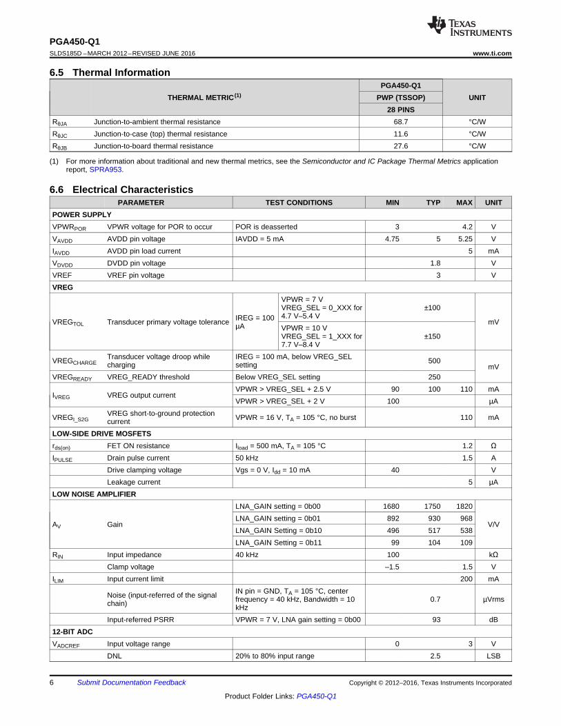
6.5 Thermal Information
THERMAL METRIC (1)PGA450-Q1
UNITPWP (TSSOP)28 PINS
RθJA Junction-to-ambient thermal resistance 68.7 °C/WRθJC Junction-to-case (top) thermal resistance 11.6 °C/WRθJB Junction-to-board thermal resistance 27.6 °C/W
6.6 Electrical CharacteristicsPARAMETER TEST CONDITIONS MIN TYP MAX UNIT
POWER SUPPLYVPWRPOR VPWR voltage for POR to occur POR is deasserted 3 4.2 VVAVDD AVDD pin voltage IAVDD = 5 mA 4.75 5 5.25 VIAVDD AVDD pin load current 5 mAVDVDD DVDD pin voltage 1.8 VVREF VREF pin voltage 3 VVREG
VREGTOL Transducer primary voltage tolerance IREG = 100µA
VPWR = 7 VVREG_SEL = 0_XXX for4.7 V–5.4 V
±100
mVVPWR = 10 VVREG_SEL = 1_XXX for7.7 V–8.4 V
±150
VREGCHARGETransducer voltage droop whilecharging
IREG = 100 mA, below VREG_SELsetting 500
mVVREGREADY VREG_READY threshold Below VREG_SEL setting 250
IVREG VREG output currentVPWR > VREG_SEL + 2.5 V 90 100 110 mAVPWR > VREG_SEL + 2 V 100 µA
VREGI_S2GVREG short-to-ground protectioncurrent VPWR = 16 V, TA = 105 °C, no burst 110 mA
LOW-SIDE DRIVE MOSFETSrds(on) FET ON resistance Iload = 500 mA, TA = 105 °C 1.2 ΩIPULSE Drain pulse current 50 kHz 1.5 A
Drive clamping voltage Vgs = 0 V, Idd = 10 mA 40 VLeakage current 5 µA
LOW NOISE AMPLIFIER
AV Gain
LNA_GAIN setting = 0b00 1680 1750 1820
V/VLNA_GAIN setting = 0b01 892 930 968LNA_GAIN Setting = 0b10 496 517 538LNA_GAIN Setting = 0b11 99 104 109
RIN Input impedance 40 kHz 100 kΩClamp voltage –1.5 1.5 V
ILIM Input current limit 200 mA
Noise (input-referred of the signalchain)
IN pin = GND, TA = 105 °C, centerfrequency = 40 kHz, Bandwidth = 10kHz
0.7 µVrms
Input-referred PSRR VPWR = 7 V, LNA gain setting = 0b00 93 dB12-BIT ADCVADCREF Input voltage range 0 3 V
DNL 20% to 80% input range 2.5 LSB

7
PGA450-Q1www.ti.com SLDS185D –MARCH 2012–REVISED JUNE 2016
Product Folder Links: PGA450-Q1
Submit Documentation FeedbackCopyright © 2012–2016, Texas Instruments Incorporated
Electrical Characteristics (continued)PARAMETER TEST CONDITIONS MIN TYP MAX UNIT
INL 20% to 80% input range, best-fit curve 4 LSBGain Best-fit curve 1373 1378 1383 LSB/VOffset Best-fit curve –15 LSB
8-BIT DACVDAC_MAX Output range 0.133 1.125 V
Gain 3.9 mV/Code
Offset voltage Output when DAC code is 000h atRload = 100 kΩ to GND 0.133 V
Full-scale voltage Output when DAC code is 0xFF Rload= 100 kΩ to GND 1.125 V
IDAC Output current DAC Code = 0x00DAC Code = 0xFF, Rload = 100 kΩ 12.5 µA
INL –2 2 LSBDNL –1 1 LSBCapacitance load 10 pF
TRANSDUCER SATURATION TIME
VSAT_TH Saturation threshold
SAT_SEL = 200 mV 200 mVSAT_SEL = 300 mV 300 mVSAT_SEL = 400 mV 400 mVSAT_SEL = 600 mV 600 mV
TEMPERATURE SENSORTemperature sensor range –40 140 °CTemperature accuracy –40°C to 105°C –5 5 °CTemperature sensor code 30°C 0 LSBTemperature sensor LSB 1.75 °C/LSB
GPIOS, 8051 UART Tx AND RxVIH GPIO input mode, high, Rx, Rload > 10 kΩ 3.5 5.3 VVIL GPIO input mode, low, Rx –0.3 1.5 VRPULLUP Internal pullup on input Pullup is to AVDD 100 KΩVOH GPIO strong-mode output, high, Tx IOH = 5 mA 4 VVOL GPIO strong-mode output, low, Tx IOL = 5 mA 0.8 V
Total current on GPIO1 + GPIO2 +Txpin No load on AVDD pin 5 mA
MEMORYOTP programming voltage 7.5 8 8.5 VOTP programming current 2 5 mA
DIAGNOSTICSVPWR_OV VPWR overvoltage level 25 28 32 VAVDD_UV VPWR for AVDD undervoltage 5.6 VAVDD_OC AVDD Overcurrent 45 55 65 mARBIAS_OC RBIAS Overcurrent 65 80 90 µA
Low-side driver A/B drain monitor 2.2 2.5 2.8 VLow-side driver A/B monitor 2.2 2.5 2.8 VOver temperature shut-off protection 150 200 ℃

8
PGA450-Q1SLDS185D –MARCH 2012–REVISED JUNE 2016 www.ti.com
Product Folder Links: PGA450-Q1
Submit Documentation Feedback Copyright © 2012–2016, Texas Instruments Incorporated
(1) LIN Mode:LIN 2.1 physical layer and LIN protocol (Section 2.1 of LIN 2.1) specificationExceptions: No wake-up (Section 2.6.2 of LIN 2.1)No transport layer in digital logic (Section 3 of LIN 2.1)No node configuration and identification services in digital (Section 4 of LIN 2.1)No diagnostic layer in digital logic (Section 5 of LIN 2.1)The device is not certified for LIN compliance. Communication baud rate is fixed at 19.2 kBPS.
(2) SCI Mode:None
6.7 Electrical Characteristics — LIN 2.1 Slave and Buffered SCI (1) (2)
PARAMETER TEST CONDITIONS MIN TYP MAX UNIT
IBUS_LIM V BUS= 18 V 40 200 mA
IBUS_PAS_dom Driver off, VBUS= 0V, VPWR= 12 V –1 mA
IBUS_PAS_recDriver off, 7 V < VPWR < 18 V, 8 V < VBUS < 18 V, VBUS >VPWR
20 µA
IBUS_NO_GND GNDDevice = V PWR, 0 < VBUS < 18 V, VPWR = 12 V –1 1 mAIBUS_NO_BAT V PWR= GND, 0 < V BUS < 18 V 100 µAVBUSdom Receiver dominant state 0.4 VPWR
VBUSrec Receiver recessive state 0.6 VPWR
VBUS_CNT VBUS_CNT = (V th_dom+ V th_rec)/2 0.475 0.5 0.525 VPWR
VHYS VHYS = Vth_rec – Vth_dom 0.175 VPWR
RSlave Serial resistor 20 30 60 KΩCIN Input capacitance on LIN pin 60 pF
6.8 Electrical Characteristics — SPI InterfacePARAMETER TEST CONDITIONS MIN TYP MAX UNITHigh-level voltage (CS, SCK, SDI,SDO) 3.5 V
Low-level voltage (CS, SCK, SDI,SDO) 1.5 V
CL(SDO) Capacitive load for data output (SDO) 10 pF
6.9 Timing RequirementsMIN NOM MAX UNIT
POWER SUPPLY
tPUPower-up time – AVDD andDVDD reach regulation levels.
VPWR = 7 V to 18 V, VREG is not inregulation 10 ms
CLOCKExternal crystal 16 MHz
FOSC Internal oscillator frequency 25°C 15.8 16 16.2 MHzFDUTY Internal oscillator duty cycle 50%
Internal oscillator frequencyaccuracy
Before LIN sync –4% 4%LIN baud rate = 19.2 kBPS, after LIN sync –0.5% 0.5%
8-bit DAC
Settling timeCode 0x00 to 0xFF step. Output is 90% offull scale. Rload = kΩ to GND. Cload = 10 pFto GND
20 µs
DIAGNOSTICS
Low-side driver A/B faultdeglitch time
LS_FAULT_TIMER_2 = 1 µs setting 1 µsLS_FAULT_TIMER_2 = 2 µs setting 2 µs
Software watchdog time-out 250 ms

9
PGA450-Q1www.ti.com SLDS185D –MARCH 2012–REVISED JUNE 2016
Product Folder Links: PGA450-Q1
Submit Documentation FeedbackCopyright © 2012–2016, Texas Instruments Incorporated
(1) LIN Mode:LIN 2.1 physical layer and LIN protocol (Section 2.1 of LIN 2.1) specificationExceptions: No wake-up (Section 2.6.2 of LIN 2.1)No transport layer in digital logic (Section 3 of LIN 2.1)No node configuration and identification services in digital (Section 4 of LIN 2.1)No diagnostic layer in digital logic (Section 5 of LIN 2.1)The device is not certified for LIN compliance. Communication baud rate is fixed at 19.2 kBPS.
(2) SCI Mode:None
6.10 Timing Requirements — LIN 2.1 Slave and Buffered SCI (1) (2)
Figure 1 shows the LIN timing details.MIN NOM MAX UNIT
D1
THRec(max) = 0.744 × VPWR; THDom(max) = 0.581 × V PWR;V PWR= 7 V...18 V; tBit= 50 µs; D1 = tBus_rec(min)/ (2 × tBit) Load1;CBUS = 1 nF; RBUS = 1KΩ Load2;CBUS = 6.8 nF; RBUS = 660 Ω Load3: CBUS = 10 nF; RBUS = 500 Ω, see Figure 1.
0.396
D2
THRec(min)= 0.522 × VPWR; THDom(min) = 0.284 × VPWR;VPWR= 7.6 V...18 V; tBit = 50 µs; D2 = tBus_rec(max)/ (2 × t Bit) Load1;CBUS = 1 nF; RBUS = 1 kΩ Load2;CBUS = 6.8 nF; R BUS = 660 Ω Load3; C BUS=10 nF; RBUS = 500 Ω, see Figure 1.
0.581
D3THRec(max) = 0.778 × VPWR; THDom(max) = 0.616 × V PWR; V PWR= 7 V to 18 V;tBit = 96 µs; D4 = tBus_rec(min) / (2 × t Bit) Load1; C BUS = 1 nF; RBUS = 1 kΩ Load2;CBUS = 6.8 nF; RBUS = 660 Ω Load3; CBUS = 10 nF; RBUS = 500 Ω, see Figure 1.
0.417
D4THRec(min) = 0.389 × VPWR; THDom(min) = 0.251 × VPWR; VPWR = 7.6 V to 18 V;tBit= 96 µs; D4 = tBus_rec(max) / (2 × t Bit) Load1; CBUS = 1 nF; RBUS = 1 kΩ Load2;CBUS = 6.8 nF; RBUS = 660 Ω Load3; CBUS = 10 nF; RBUS = 500 Ω, see Figure 1.
0.590
trx_pdPropagation delay of receiverRRXD = 2.4 kΩ; CRXD = 20 pF
6 µs
trx_symSymmetry of receiver propagation delay rising edge with respect to falling edgeRRXD = 2.4 kΩ; C RXD = 20 pF
–2 2 µs

10
PGA450-Q1SLDS185D –MARCH 2012–REVISED JUNE 2016 www.ti.com
Product Folder Links: PGA450-Q1
Submit Documentation Feedback Copyright © 2012–2016, Texas Instruments Incorporated
6.11 Timing Requirements — SPI InterfaceFigure 2 shows the SPI clocking details.
MIN NOM MAX UNITfSCK SPI frequency 8 MHztCSSCK CS low to first SCK rising edge
See Figure 2.
125 nstSCKCS Last SCK rising edge to CS rising edge 125 nstCSD CS disable time 375 nstDS SDI setup time 25 nstDH SDI hold time 25 nstSDIS SDI fall/rise time 25 nstSCKR SCK rise time 7 nstSCKF SCK fall time 7 nstSCKH SCK high time 62.5 nstSCKL SCK low time 62.5 nstSDO SDO enable time 25 nstACCS SCK rising edge to SDO data valid 25 nstSDOD SDO disable time 25 nstSDOS SDO rise/fall time CSDO = 10 pF, see Figure 2. 1 15 ns
6.12 Switching Characteristicsover operating free-air temperature range (unless otherwise noted)
PARAMETER TEST CONDITIONS MIN TYP MAX UNIT12-BIT ADC
Conversion time 1 µs8051W WARP COREFCORE_CLK Core frequency 16 MHz
Memory interface 1 Wait StateMEMORY
OTP programming time 1 byte 100 µsOTP data retention years 105 °C 10 YearsEEPROM R/W cycles 1000 CyclesEEPROM data retention 105 °C 10 YearsEEPROM programming time 32 Bytes 70 ms
DIAGNOSTICSMain oscillator underfrequency fault 14 MHzMain oscillator overfrequency fault 18 MHz
6.13 Digital Datapath Filter Switching CharacteristicsPARAMETER TEST CONDITIONS MIN TYP MAX UNIT
BAND-PASS FILTERFILTER TYPE: SECOND-ORDER BUTTERWORTH FILTERBand-pass center frequency 40 70 kHzBand-pass center-frequency step size 0.5 kHzBandpass filter bandwidth 4 7 kHzBandpass filter bandwidth step size 0.5 kHzBPF gain 0 dBDOWNSAMPLEDownsample rate 25 50 SamplesDownsample-rate step size 1

VPWR
TXD (Input)
LIN Bus Signal
RXDD1 (20 kbps) andD3 (10 kbps) case
RXDD2 (20 kbps) andD4 (10 kbps) case
tBit tBit
THRec(max)
THRec(min)
THDom(max)
THDom(min)
tBus_rec(max)
tBus_dom(min) tBus_rec(min)
tBus_dom(max)
Bus_rec(min)
Bit
tD =
(2 t )u
Bus_rec(max)
Bit
tD =
(2 t )u
Thresholdsworst case 1
Thresholdsworst case 2
D = 0.5
RECESSIVE
DOMINANT
trx_pdf(1)
trx_pdr(2)
trx_pdr(1)
trx_pdf(2)
11
PGA450-Q1www.ti.com SLDS185D –MARCH 2012–REVISED JUNE 2016
Product Folder Links: PGA450-Q1
Submit Documentation FeedbackCopyright © 2012–2016, Texas Instruments Incorporated
Digital Datapath Filter Switching Characteristics (continued)PARAMETER TEST CONDITIONS MIN TYP MAX UNIT
LOW-PASS FILTERFILTER TYPE: FIRST-ORDER BUTTERWORTH FILTERLPF cutoff frequency 0.5 4 kHzLPF cutoff frequency step size 0.5 kHzLPF gain 0 dB
Figure 1. LIN Timing Diagram

LSB
LSBMSB
MSB
CS
SCK
SDI
SDO
tCSSCK tSCKRtSCKF
tDS tDH
tSDIS
tSDOE
tACCS
tSDOS
tCSD
tSCKL
tSCKCS
tSCKH
tSDOD
12
PGA450-Q1SLDS185D –MARCH 2012–REVISED JUNE 2016 www.ti.com
Product Folder Links: PGA450-Q1
Submit Documentation Feedback Copyright © 2012–2016, Texas Instruments Incorporated
Figure 2. SPI Clocking Details

Seconds
Cou
nts
0
500
1000
1500
2000
2500
0 3.3 3.53.4× 10±3 Seconds
Cou
nts
0
500
1000
1500
2000
2500
3.8 3.9 4× 10±3
Time (ms)
µV
-3
-2
-1
0
1
2
3
0 2 4 6 8 12 1610 14ADC Code
LSB
-5
-4
-3
-2
-1
0
1
2
3
4
0 500 1000 1500 2000 2500 3500 45003000 4000
13
PGA450-Q1www.ti.com SLDS185D –MARCH 2012–REVISED JUNE 2016
Product Folder Links: PGA450-Q1
Submit Documentation FeedbackCopyright © 2012–2016, Texas Instruments Incorporated
6.14 Typical CharacteristicsVPWR = 12 V, TA = 25°C
Input referred LNA AC noise in 10-kHz bandwidth around 40 kHzVnoise = 0.7 µVrms
Figure 3. LNA Noise Figure 4. ADC INL
BPF center frequency = 58 kHz BPF bandwidth = 7 kHz
Figure 5. Datapath Output, Downsample Rate = 40
BPF center frequency = 58 kHz BPF bandwidth = 7 kHz
Figure 6. Datapath Output, Downsample Rate = 25

LNA1500V/VSAR
Thermal Shutdown
EEPROM
Driver 1
Driver 2
LIN 2.1 Transciever
DIGITAL
SUPPLY VOLTAGE
LIN
IN
OUTA
OUTB
GNDGND
VREG
CS
SCLK
SDO
SDI
ad
uP Rx uP Tx
clk DVDD
AVDD
over_temp
over_temp
over_temp
reset
GPIO1
GPIO2
uP GPIO
uP GPIO
TxDuP Tx
CIN
RxDuP Rx
DACO
Voltage Regulator Primary
VPWR
DVDD
100 nF
AVDD
100 nF
100 nF
VREF
VREF
OTP
ANALOG
LIM
rxtx
MEMORY
Clock Synchronizer
XIN
XOUT
pwmb
pwma
Cc Rs
RBIAS
100 K
DEV. RAMRAM
DIGITAL DATAPATH
clk_sel
temp_ad
FIFO RAM
COMP
peak
saturation time
100 nF
+
±
FIFO RAM
PROGRAMMING VOLTAGE FOR OTP
VPROG_OTP
GND
gnd
gnd
gnd
Saturation Time Measurement
GND
16-MHz Internal
Oscillator
XTAL Interface
clk
CLOCK
INT_CLK
EXT_CLK
x� Linear Regulatorsx� Bandgap Referencex� Precision Biasx� POR
Power Supply
uCONTROLLER
UART
Burst Generator
Watchdog LIN 2.1 Slave Protocol
orBuffered SCI
Temperature Sensor
MU
X
14
PGA450-Q1SLDS185D –MARCH 2012–REVISED JUNE 2016 www.ti.com
Product Folder Links: PGA450-Q1
Submit Documentation Feedback Copyright © 2012–2016, Texas Instruments Incorporated
7 Detailed Description
7.1 OverviewThe PGA450-Q1 integrates power management, low-side drivers, analog front-end, digital datapath, andinterface functions to form a full ultrasonic-sensor signal conditioning solution. The low-side drivers areprogrammed to drive a specific frequency that matches the external ultrasonic transducer. After transmitting, thesame transducer receives the reflected echo signal. The analog front-end filters and amplifies this signal beforestoring the data in memory. The integrated 8051 microcontroller then processes this data to extract the usefulinformation which typically includes how far away an object is from the transducer. At this point in the process,the information is transmitted through LIN, SCI, or UART.
7.2 Functional Block Diagram

Ref + Bias circuitry
AVDD Regulator
DVDD Regulator
Internal Oscillator
Power on reset
VPWR
RBIAS
AVDD
DVDD
Ref + Bias AVDD DVDD Internal CLK POR
VREF Regulator VREF
15
PGA450-Q1www.ti.com SLDS185D –MARCH 2012–REVISED JUNE 2016
Product Folder Links: PGA450-Q1
Submit Documentation FeedbackCopyright © 2012–2016, Texas Instruments Incorporated
7.3 Feature Description
7.3.1 Power Supply BlockThe PGA450-Q1 uses three internal regulators (AVDD, DVDD, and VREF) as supplies for all of the internalcircuits. The power-supply block also generates a precision voltage reference, current bias, and internal clock.The internal power-on-reset (POR) signal is released when the internal power supplies, voltage reference,current bias, and internal clock come into regulation.
Figure 7 shows the relationships of the power supplies and the POR signal in the PGA450-Q1 device.
Figure 7. Power-Supply Block
The PGA450-Q1 begins to power up when a voltage is applied to the VPWR pin. Figure 8 shows a typicalpower-up diagram. The power-up time is typically about 3 ms.

VPWR
See (1)
See (2)
See (3)
POR releasetime
(1 ms)
Power supply monitor check
(2 ms)
See (4)
External RAM MBIST (5 ms)
8051 Reset
Internal Reset
16
PGA450-Q1SLDS185D –MARCH 2012–REVISED JUNE 2016 www.ti.com
Product Folder Links: PGA450-Q1
Submit Documentation Feedback Copyright © 2012–2016, Texas Instruments Incorporated
Feature Description (continued)
(1) ACTIVE_EN bit must be set before enabling the burst / saturation or echo-enable bits.
(1) The VPWR ramp reaches POR level.(2) The internal reset to the digital core is released and EXTERNAL RAM MBIST is initiated. SPI communication is
available.(3) 8051W reset is deasserted. Software starts execution.(4) EXTERNAL RAM MBIST is complete. External Scratchpad RAM and FIFO RAM available for use.
Figure 8. Power-Up Waveforms
The PGA450-Q1 provides two power-control bits for enabling different analog blocks to manage the total currentconsumption of the device. On power up, the device is in the QUIET mode with only the 8051W and LINtransceiver turned on. All other analog blocks are disabled. Setting the ACTIVE_EN bit enables the low-sidedrivers required for bursting as well as the echo-processing circuitry that includes the LNA and the ADC. Inaddition, a separate control bit, VREG_EN, is provided to enable the VREG circuitry, which is used to charge theexternal capacitor used during bursting.
The AVDD pin can be used to source current for up to 5 mA for resistive loads, including the loads on the GPIOand Tx pins.
Table 1. Power ModesCONTROL BIT DEFAULT FUNCTION
1 VREG_EN Disabled Enables the VREG circuitry that provides the 100-mA current tocharge the external capacitor used during bursting
2 ACTIVE_EN (1) Disabled Enables the LNA, ADC, ADC REF, and other support circuitry relatedto burst generation and echo processing
7.3.2 VREGThe PGA450-Q1 provides a regulated voltage output which, along with an external capacitor, can be used todrive the primary of the transformer used to excite the transducer. The VREG regulator provides a 100-mAcurrent, sourced from VPWR, to charge the external capacitor. The user can select the desired VREG voltage bysetting the VREG_SEL register to the appropriate value.
For VREG to be regulated to the selected voltage, VPWR must be at least 2 V above the selected VREGvoltage.
The energy required for the burst comes from the external capacitor. The device has a VREG_READY status bitin the STATUS2 register to indicate when the capacitor is fully charged and has reached the regulation voltage.

X 1
X 2 MUXclk
CLOCKclk_sel
INT CLK
EXT CLK
ClockSynchronizer
16-MHzInternal
Oscillator
XTALInterface
VPWR
VREG
100 mA
VREG_SEL Voltage
VREG Capacitor
17
PGA450-Q1www.ti.com SLDS185D –MARCH 2012–REVISED JUNE 2016
Product Folder Links: PGA450-Q1
Submit Documentation FeedbackCopyright © 2012–2016, Texas Instruments Incorporated
Figure 9. VREG Regulator
This block is disabled by default. Setting the VREG_EN bit in the PWR_MODE register to high, enables thisregulator.
7.3.3 ClockThe clock block generates the system clock that is used in the generation of burst, communication, echo timemeasurement, and the microprocessor clock. Figure 10 shows the clock block in the PGA450-Q1.
Figure 10. Clock Block in PGA450-Q1
The CLK signal provided to various blocks inside the device is derived from one of the following sources:1. Internal oscillator without synchronization with communication: in this mode, the internal oscillator output is
the source for the system clock.2. Internal oscillator with synchronization with communication: in this mode, the internal oscillator output is
corrected for inaccuracy using time measurements of the communication bus. This mode requires theimplementation of CLOCK SYNCHRONIZER logic in the digital control block. The clock synchronizer usesthe SYNC FIELD to measure the timer value and adjust the internal oscillator output.
3. External crystal: in this mode, a 16-MHz external crystal is the source of the system clock.
The clock source is controlled by the CLK_SEL register. Table 2 lists the settings of the CLK_SEL bits and thecorresponding clock mode.

OS5:0 bits in OSC_SYNC_CTRL
ESFRInternal Oscillator
I clk
Digital ControlLIN SYNC Field
OSC SYNC Value
8051W
OVR bit in OSC_SYNC_CTRL ESFR
SYNC_COUNT ESFR
18
PGA450-Q1SLDS185D –MARCH 2012–REVISED JUNE 2016 www.ti.com
Product Folder Links: PGA450-Q1
Submit Documentation Feedback Copyright © 2012–2016, Texas Instruments Incorporated
Table 2. Clock SelectionCLK_SEL BIT VALUES CLOCK SOURCE
0b00 Internal clock. Ignore the synchronization pulse received on the LIN bus.0b01 Internal clock. Process the synchronization pulse received on the LIN bus.0b10 External crystal clock0b11 Internal clock. Ignore the synchronization pulse received on the LIN bus.
7.3.3.1 Clock Synchronizer Using the SYNC Field in the LIN BusThe clock synchronizer block adjusts the internal oscillator based on a SYNC field in the LIN frame received inthe communication line. The internal clock is trimmed to 16 MHz with ±4% tolerance in the TI factory.
The clock synchronizer improves the instantaneous accuracy of the internal oscillator frequency to 16 MHz±0.5% using the LIN SYNC field, assuming an ideal LIN baud rate of 19.2 kBPS. The synchronization algorithmuses the time between two falling edges of the LIN SYNC field to adjust the internal oscillator.
The SYNC_COUNT is available for the 8051W to determine the effectiveness of the synchronization processbased on the LIN SYNC field. That is, if the synchronization was effective, then the SYNC COUNT value shouldbe close to 1667 ±8 counts.
This OSC SYNC value can also be updated by the 8051W microprocessor by setting the OVR bit inOSC_SYNC_CTRL ESFR.
Figure 11. PGA450-Q1 Internal Clock Synchronization Control
Table 3 lists the value of OS<5:0> and the resulting change in frequency.
Table 3. OS<5:0> versus Delta System Clock FrequencyOS<5:0> Delta Frequency
0 –3.84 MHz.. ..31 –120 kHz32 0 kHz33 120 kHz.. ..63 3.72 MHz
Gate Control Logic
2.5 VOUTx
GND
LS Driver
DRAIN _MON
GATE _MON
LSG _EN
LSG
+
+
19
PGA450-Q1www.ti.com SLDS185D –MARCH 2012–REVISED JUNE 2016
Product Folder Links: PGA450-Q1
Submit Documentation FeedbackCopyright © 2012–2016, Texas Instruments Incorporated
NOTEThe clock synchronization feature is not available if the device is configured in SCIbuffered mode. See the LIN 2.1 Slave and Buffered SCI section for details.
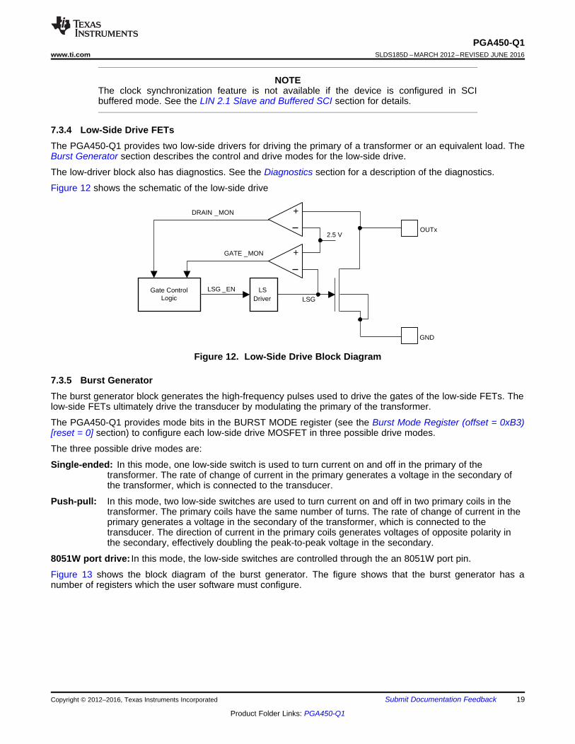
7.3.4 Low-Side Drive FETsThe PGA450-Q1 provides two low-side drivers for driving the primary of a transformer or an equivalent load. TheBurst Generator section describes the control and drive modes for the low-side drive.
The low-driver block also has diagnostics. See the Diagnostics section for a description of the diagnostics.
Figure 12 shows the schematic of the low-side drive
Figure 12. Low-Side Drive Block Diagram
7.3.5 Burst GeneratorThe burst generator block generates the high-frequency pulses used to drive the gates of the low-side FETs. Thelow-side FETs ultimately drive the transducer by modulating the primary of the transformer.
The PGA450-Q1 provides mode bits in the BURST MODE register (see the Burst Mode Register (offset = 0xB3)[reset = 0] section) to configure each low-side drive MOSFET in three possible drive modes.
The three possible drive modes are:
Single-ended: In this mode, one low-side switch is used to turn current on and off in the primary of thetransformer. The rate of change of current in the primary generates a voltage in the secondary ofthe transformer, which is connected to the transducer.
Push-pull: In this mode, two low-side switches are used to turn current on and off in two primary coils in thetransformer. The primary coils have the same number of turns. The rate of change of current in theprimary generates a voltage in the secondary of the transformer, which is connected to thetransducer. The direction of current in the primary coils generates voltages of opposite polarity inthe secondary, effectively doubling the peak-to-peak voltage in the secondary.
8051W port drive: In this mode, the low-side switches are controlled through the an 8051W port pin.
Figure 13 shows the block diagram of the burst generator. The figure shows that the burst generator has anumber of registers which the user software must configure.

Oscillator
8051W BURST Generator
ON_B
PULSE_CNTB
clk
ADDRESS/DATA BUS
BURST OUTB
ON_A
PULSE_CNTABURST OUTA
OFF_A
OFF_B
DEADTIME
EN_CTRL
P2.1
P2.0
BURST_MODE
Burst Mode Bits
Burst Mode Bits
20
PGA450-Q1SLDS185D –MARCH 2012–REVISED JUNE 2016 www.ti.com
Product Folder Links: PGA450-Q1
Submit Documentation Feedback Copyright © 2012–2016, Texas Instruments Incorporated
Figure 13. Burst Generator
The PGA450-Q1 provides 3 mode bits in the BURST MODE register to select from the five burst configurationsavailable. Table 4 lists the modes of operation of the two low-side gate drives of the burst generator. For anunderstanding of the configurations, see Figure 14 and for an understanding of the waveforms, see Figure 15.
Table 4. Low-Side MOSFET Gate Drive ModesITEM DESCRIPTION
Mode Bits in BURST_MODE Register: 000Mode description Low-side A and B are in push-pullLow-side A trigger Write 1 to BURST_A_EN bit in EN_CTRL registerLow-side B trigger Write 1 to BURST_A_EN bit in EN_CTRL registerNo. of pulses on A Set by PULSE_CNTA (0–63 pulses) registerNo. of pulses on B Set by PULSE_CNTB (0–63 pulses) register
Low-side A frequency
Set by registers:● ON_A (11 bits at 16 MHz)● OFF_A (11 bits at 16 MHz)● DEADTIME (8 bits at 16 MHz)
Low-side B frequency Set by registers: ON_A (11 bits at 16 MHz), OFF_A (11 bits at 16 MHz), DEADTIME(8 bits at 16 MHz)
Mode Bits in BURST_MODE Register: 001
Mode description Low-side A is controlled by burst generator ALow-side B through the internal micro P2.1 port
Low-side A trigger Write 1 to BURST_A_EN bit in EN_CTRL registerLow-side B trigger Controlled by 8051W softwareNo. of pulses on A Set by PULSE_CNTA (0–63 pulses) registerNo. of pulses on B Controlled by 8051W software

BURST OUTx
ON
OFFN = Pulse Count
1 2 3 4 5 N
21
PGA450-Q1www.ti.com SLDS185D –MARCH 2012–REVISED JUNE 2016
Product Folder Links: PGA450-Q1
Submit Documentation FeedbackCopyright © 2012–2016, Texas Instruments Incorporated
Table 4. Low-Side MOSFET Gate Drive Modes (continued)ITEM DESCRIPTION
Low-side A frequencySet by registers:● ON_A (11 bits at 16 MHz)● OFF_A (11 bits at 16 MHz)
Low-side B frequency Controlled by 8051W softwareMode Bits in BURST_MODE Register: 010
Mode description Low-side A through the internal micro P2.0 portLow-side B is controlled by burst generator B
Low-side A trigger Controlled by 8051W softwareLow-side B trigger Write 1 to BURST_B_EN bit in EN_CTRL registerNo. of pulses on A Controlled by 8051W softwareNo. of pulses on B Set by PULSE_CNTB (0–63 pulses) registerLow-side A frequency Controlled by 8051W softwareLow-side B frequency Set by registers: ON_B (11 bits at 16 MHz) and OFF_B (11 bits at 16 MHz)Mode Bits in BURST_MODE Register: 011
Mode description Low-side A is controlled by burst generator ALow-side B is controlled by burst generator B
Low-side A trigger Write 1 to BURST_A_EN bit in EN_CTRL registerLow-Side B trigger Write 1 to BURST_B_EN bit in EN_CTRL registerNo. of pulses on A Set by PULSE_CNTA (0–63 pulses) registerNo. of pulses on B Set by PULSE_CNTB (0–63 pulses) registerLow-side A frequency Set by registers: ON_A (11 bits at 16 MHz) and OFF_A (11 bits at 16 MHz)Low-side B frequency Set by registers: ON_B (11 bits at 16 MHz) and OFF_B (11 bits at 16 MHz)Mode Bits in BURST_MODE Register: 100
Mode description Low-side A through the internal micro P2.0 portLow-side B through the internal micro P2.1 port
Low-side A trigger Controlled by 8051W softwareLow-side B trigger Controlled by 8051W softwareNo. of pulses on A Controlled by 8051W softwareNo. of pulses on B Controlled by 8051W softwareLow-side A frequency Controlled by 8051W softwareLow-side B frequency Controlled by 8051W softwareMode Bits in BURST_MODE Register: 101Mode description ReservedMode Bits in BURST_MODE Register: 110Mode description ReservedMode Bits in BURST_MODE Register: 111Mode description Reserved
Figure 14 shows the relationship of BURST_OUTx.
Figure 14. Timing Diagram Showing the Usage of ON Register, OFF Register and PULSE COUNTRegister Values

IN
Bias Voltage
CIN
+
±
To ADC
From transducer
LNA_GAIN<1:0> bits inCONTROL_1 ESFR
OFF_A
ON_A
OFF_AON_A
FET1
FET2
DEADTIME
22
PGA450-Q1SLDS185D –MARCH 2012–REVISED JUNE 2016 www.ti.com
Product Folder Links: PGA450-Q1
Submit Documentation Feedback Copyright © 2012–2016, Texas Instruments Incorporated
The relationship between the ONTIME, OFFTIME, and DEADTIME values in the push-pull configurations areshown in Figure 15.
Figure 15. Timing Diagram Showing the Relationship Between ONTIME, OFFTIME, and DEADTIMERegisters in the Push-Pull Configuration
Table 5 lists the 8051W port pins used to drive the OUTA and OUTB pins are listed in the 8051W drive mode.
Table 5. OUTA/OUTB Pin MapPGA450-Q1 PIN 8051W PORT
OUTA 2.0OUTB 2.1
7.3.6 Low-Noise AmplifierThis block is the analog front-end that interfaces with the transducer directly. The echo signal is coupled throughan external capacitor so that only the AC component of the transducer voltage is passed to the low-noiseamplifier (LNA). The LNA outputs an amplified version of the transducer voltage with a DC offset that is equal tothe mid-scale of the analog-to-digital converter (ADC).
The LNA gain is configurable by setting the LNA_GAIN1 and LNA_GAIN0 bits in the CONTROL_1 register to theappropriate values.
Figure 16. Low-Noise Amplifier
7.3.7 Analog-to-Digital ConverterThe 12-bit successive approximation register (SAR) analog-to-digital converter converts the analog voltage fromthe echo-processing circuit into a digital word. The converted digital word is processed by the bandpass filter.The ADC is dedicated to the echo-processing signal path and is only enabled in active mode.
7.3.8 Digital Data PathThe digital datapath processes the AD sample to extract the peak profile of the echo. The output of the digitaldatapath is stored in the FIFO RAM.

SAR ADC
Band-pass Filter Rectifier Peak Extractor Downsample Low-pass Filter
Butterworth IIR
Second Order
Gain = 1
CF = 40 Khz .. 0.5 Khz .. 70 KHz
BW =
DS Rate: 25..1..50 Butterworth IIR
First Order
Gain = 1
Cutoff:
500 Hz .. 500 Hz .. 4000 Hz
1 MHz1/DS MHz 1/DS MHz
FIFO RAM
Digital Datapath
4 Khz .. 0.5 Khz .. 7 KHz
23
PGA450-Q1www.ti.com SLDS185D –MARCH 2012–REVISED JUNE 2016
Product Folder Links: PGA450-Q1
Submit Documentation FeedbackCopyright © 2012–2016, Texas Instruments Incorporated
Figure 17 shows the digital datapath.
Figure 17. Digital Data Path
The digital datapath has the following components:• Bandpass filter• Rectifier• Peak extractor• Downsampler• Low-pass filter
Each of the digital datapath components is described in the following subsections.
7.3.8.1 Bandpass Filter (BPF)The echo signal is an amplitude-modulated signal with the underlying carrier frequency equal to the drivefrequency of the ultrasonic transducer. The bandpass filter block allows frequencies near the drive frequency topass to downstream signal blocks.
The bandpass filter is a second-order Butterworth IIR filter. The user can configure the center frequency and thebandwidth of the filter by writing specific values to coefficient registers BPF_B1, BPF_A2, and BPF_A3.
Table 7 lists the values (in hex) that must be written to the coefficient registers to realize a bandpass filter ofspecific center frequency and bandwidth (or Q).
NOTEThe stability of the filter is not assured if values other than those listed in Table 7 arewritten to the registers.
Table 6. Bandpass Filter Coefficient ValuesBW (kHz) B1 (Hex) A3 (Hex)
4 32D F9A54.5 392 F8DD5 3F6 F815
5.5 459 F74D6 4BD F687
6.5 520 F5C17 582 F4FB

24
PGA450-Q1SLDS185D –MARCH 2012–REVISED JUNE 2016 www.ti.com
Product Folder Links: PGA450-Q1
Submit Documentation Feedback Copyright © 2012–2016, Texas Instruments Incorporated
Table 7. Bandpass Filter Coefficient ValuesCF (kHz) BW (kHz) A2 (Hex)
39
4 F54A5 F48B6 F3CD7 F311
40
4 F4E65 F4276 F36A7 F2AE
41
4 F4805 F3C16 F3047 F249
42
4 F4175 F3586 F29C7 F1E1
43
4 F3AC5 F2ED6 F2317 F176
44
4 F33E5 F2806 F1C47 F10A
45
4 F2CE5 F2106 F1547 F09A
46
4 F25B5 F19E6 F0E27 F029
47
4 F1E65 F1296 F06E7 EFB5
48
4 F16E5 F0B26 EFF77 EF3E
49
4 F0F45 F0386 EF7E7 EEC5

25
PGA450-Q1www.ti.com SLDS185D –MARCH 2012–REVISED JUNE 2016
Product Folder Links: PGA450-Q1
Submit Documentation FeedbackCopyright © 2012–2016, Texas Instruments Incorporated
Table 7. Bandpass Filter Coefficient Values (continued)CF (kHz) BW (kHz) A2 (Hex)
50
4 F0785 EFBC6 EF027 EE4A
51
4 EFF95 EF3E6 EE847 EDCC
52
4 EF785 EEBD6 EE037 ED4C
53
4 EEF45 EE396 ED807 ECC9
54
4 EE6E5 EDB46 ECFB7 EC44
55
4 EDE55 ED2B6 EC737 EBBD
56
4 ED5A5 ECA16 EBE97 EB33
57
4 ECCD5 EC146 EB5D7 EAA7
58
4 EC3D5 EB856 EACE7 EA19
59
4 EBAB5 EAF36 EA3D7 E988
60
4 EB165 EA5F6 E9A97 E8F5

26
PGA450-Q1SLDS185D –MARCH 2012–REVISED JUNE 2016 www.ti.com
Product Folder Links: PGA450-Q1
Submit Documentation Feedback Copyright © 2012–2016, Texas Instruments Incorporated
Table 7. Bandpass Filter Coefficient Values (continued)CF (kHz) BW (kHz) A2 (Hex)
61
4 EA7F5 E9C86 E9137 E85F
62
4 E9E65 E9306 E87B7 E7C7
63
4 E94B5 E8946 E7E07 E72D
64
4 E8AD5 E7F76 E7437 E691
65
4 E80C5 E7576 E6A47 E5F2
66
4 E7695 E6B56 E6027 E551
67
4 E6C45 E6106 E55E7 E4AD
68
4 E61D5 E5696 E4B87 E407
69
4 E5735 E4C06 E40F7 E35F
70
4 E4C75 E4156 E3647 E2B5

Z±1
>
y(k±1)
y(k)
x(k)
Reset
27
PGA450-Q1www.ti.com SLDS185D –MARCH 2012–REVISED JUNE 2016
Product Folder Links: PGA450-Q1
Submit Documentation FeedbackCopyright © 2012–2016, Texas Instruments Incorporated
7.3.8.2 RectifierThe output of the bandpass filter is a signed number. The rectifier rectifies the output of the bandpass filter tocreate a positive number.
7.3.8.3 Peak ExtractorThe peak extractor in the PGA450-Q1 is a simple moving-peak algorithm. Specifically, the output of the peakextractor is updated if the input to the peak extractor is greater than the previous output of the peak extractor.This algorithm is summarized in Equation 1.
y[k] = {y[k – 1], if y[k – 1] > Px[k], otherwise x[k]}
where• y is the output of the peak extractor• x is the input to the peak extractor• k is the discrete-time step (1)
Figure 18 shows the peak extractor algorithm.
Figure 18. Peak Extractor
7.3.8.4 DownsampleThe downsample block performs two functions:• Generates the reset signal for the peak extractor shown in Figure 18.• Generates the output.
The downsample rate can be configured by the user by writing to the downsample register. If the output of thepeak extractor must be low-pass filtered before storing it in the FIFO, then the allowable values for thedownsample register for the low-pass filter correctly are from 25 to 50; that is:
25 ≤ DOWNSAMPLE ≤ 50 (2)
However, if the user does not need to low-pass filter the output before storing to the FIFO, then the user canconfigure the DOWNSAMPLE register value to any value between 1 and 63.
The downsample block has a counter which starts at 0 and counts up to the values programmed in theDOWNSAMPLE register. When the count reaches the value in the DOWNSAMPLE register, the counter insidethe downsample block is reset to 0. Furthermore, the downsample block generates a reset to the peak extractor.This reset signal sets the output of the peak extractor to 0.
The data output rate of the downsample block is:OUTPUT RATE OF DOWNSAMPLE RATE = DOWNSAMPLE × 1 µs. (3)
7.3.8.5 Low-Pass FilterThe output of the downsample block can be filtered by a low-pass filter. The low-pass filter in the PGA450-Q1device is a first-order Butterworth IIR filter with a configurable cutoff frequency.
The user can configure the cutoff frequency of the filter by writing specific values to coefficient registers LPF_B1and LPF_A2. Note that for the same desired cutoff frequency, the coefficient values depend on the configuredDOWNSAMPLE register.

28
PGA450-Q1SLDS185D –MARCH 2012–REVISED JUNE 2016 www.ti.com
Product Folder Links: PGA450-Q1
Submit Documentation Feedback Copyright © 2012–2016, Texas Instruments Incorporated
Table 8 lists the values (in hex) that must be written to the coefficient registers to realize a low-pass filter of aspecific cutoff frequency. The stability of the filter is not assured if values other than those listed in the table arewritten to the registers.
Table 8. Low-Pass Filter Coefficient Values
CUTOFF (kHz) DOWNSAMPLE (Hex) B1 (Hex) A2 (Hex)
0.5 19 4D7 7652
1A 506 75F3
1B 536 7594
1C 565 7535
1D 595 74D7
1E 5C4 7479
1F 5F3 741B
20 622 73BD
21 650 7360
22 67F 7302
23 6AD 72A5
24 6DC 7249
25 70A 71EC
26 738 7190
27 766 7134
28 794 70D9
29 7C1 707E
2A 7EF 7022
2B 81C 6FC8
2C 84A 6F6D
2D 877 6F13
2E 8A4 6EB9
2F 8D1 6E5F
30 8FD 6E05
31 92A 6DAC
32 957 6D53

29
PGA450-Q1www.ti.com SLDS185D –MARCH 2012–REVISED JUNE 2016
Product Folder Links: PGA450-Q1
Submit Documentation FeedbackCopyright © 2012–2016, Texas Instruments Incorporated
Table 8. Low-Pass Filter Coefficient Values (continued)CUTOFF (kHz) DOWNSAMPLE (Hex) B1 (Hex) A2 (Hex)
1.0 19 957 6D53
1A 9B0 6CA1
1B A08 6BF0
1C A60 6B41
1D AB7 6A92
1E B0E 69E5
1F B64 6937
20 BBA 688B
21 C10 67E0
22 C65 6736
23 CBA 668C
24 D0E 65E4
25 D62 653C
26 DB6 6495
27 E09 63EF
28 E5B 6349
29 EAE 62A5
2A EFF 6201
2B F51 615E
2C FA2 60BC
2D FF3 601B
2E 1043 5F7A
2F 1093 5EDA
30 10E2 5E3B
31 1132 5D9D
32 1180 5CFF

30
PGA450-Q1SLDS185D –MARCH 2012–REVISED JUNE 2016 www.ti.com
Product Folder Links: PGA450-Q1
Submit Documentation Feedback Copyright © 2012–2016, Texas Instruments Incorporated
Table 8. Low-Pass Filter Coefficient Values (continued)CUTOFF (kHz) DOWNSAMPLE (Hex) B1 (Hex) A2 (Hex)
1.5 19 D8C 64E8
1A E09 63EF
1B E84 62F7
1C EFF 6201
1D F79 610D
1E FF3 601B
1F 106B 5F2A
20 1000 5E3B
21 1159 5D4E
22 11CF 5C62
23 1244 5B78
24 12B8 5A90
25 132C 59A9
26 139E 58C4
27 1410 57E0
28 1481 56FD
29 14F2 561C
2A 1562 553D
2B 15D1 545E
2C 163F 5381
2D 16AD 52A6
2E 171A 51CC
2F 1786 50F3
30 17F2 501C
31 185D 4F45
32 18C8 4E70

31
PGA450-Q1www.ti.com SLDS185D –MARCH 2012–REVISED JUNE 2016
Product Folder Links: PGA450-Q1
Submit Documentation FeedbackCopyright © 2012–2016, Texas Instruments Incorporated
Table 8. Low-Pass Filter Coefficient Values (continued)CUTOFF (kHz) DOWNSAMPLE (Hex) B1 (Hex) A2 (Hex)
2.0 19 1180 5CFF
1A 121D 5BC6
1B 12B8 5A90
1C 1352 595C
1D 13EA 582B
1E 1481 56FD
1F 1517 55D1
20 15AC 54A8
21 163F 5381
22 16D1 525D
23 1762 513B
24 17F2 501C
25 1881 4EFE
26 190F 4DE3
27 199B 4CCA
28 1A27 4BB3
29 1AB1 4A9E
2A 1B3A 498B
2B 1BC3 487A
2C 1C4A 476B
2D 1CD1 465E
2E 1D56 4553
2F 1DDB 444A
30 1E5F 4342
31 1EE2 423C
32 1F64 4138

32
PGA450-Q1SLDS185D –MARCH 2012–REVISED JUNE 2016 www.ti.com
Product Folder Links: PGA450-Q1
Submit Documentation Feedback Copyright © 2012–2016, Texas Instruments Incorporated
Table 8. Low-Pass Filter Coefficient Values (continued)CUTOFF (kHz) DOWNSAMPLE (Hex) B1 (Hex) A2 (Hex)
2.5 19 153D 5587
1A 15F6 5415
1B 16AD 52A6
1C 1762 513B
1D 1816 4FD4
1E 18C8 4E70
1F 1978 4D10
20 1A27 4BB3
21 1AD3 4A59
22 1B7F 4903
23 1C29 47AF
24 1CD1 465E
25 1D78 4511
26 1E1D 43C6
27 1EC1 427E
28 1F64 4138
29 2005 3FF5
2A 20A6 3EB5
2B 2145 3D77
2C 21E2 3C3B
2D 227F 3B02
2E 231A 39CB
2F 23B5 3897
30 244E 3764
31 24E6 3633
32 257E 3505

33
PGA450-Q1www.ti.com SLDS185D –MARCH 2012–REVISED JUNE 2016
Product Folder Links: PGA450-Q1
Submit Documentation FeedbackCopyright © 2012–2016, Texas Instruments Incorporated
Table 8. Low-Pass Filter Coefficient Values (continued)CUTOFF (kHz) DOWNSAMPLE (Hex) B1 (Hex) A2 (Hex)
3.0 19 18C8 4E70
1A 199B 4CCA
1B 1A6C 4B28
1C 1B3A 498B
1D 1C07 47F3
1E 1CD1 465E
1F 1D99 44CE
20 1E5F 4342
21 1F23 41BA
22 1FE5 4036
23 20A6 3EB5
24 2164 3D38
25 2221 3BBE
26 22DC 3A47
27 2396 38D4
28 244E 3764
29 2505 35F7
2A 25BA 348D
2B 266E 3325
2C 2720 31C0
2D 27D1 305E
2E 2881 2EFE
2F 292F 2DA1
30 29DD 2C46
31 2A89 2AED
32 2B35 2997

34
PGA450-Q1SLDS185D –MARCH 2012–REVISED JUNE 2016 www.ti.com
Product Folder Links: PGA450-Q1
Submit Documentation Feedback Copyright © 2012–2016, Texas Instruments Incorporated
Table 8. Low-Pass Filter Coefficient Values (continued)CUTOFF (kHz) DOWNSAMPLE (Hex) B1 (Hex) A2 (Hex)
3.5 19 1C29 47AF
1A 1D14 45D9
1B 1DFC 4408
1C 1EE2 423C
1D 1FC5 4076
1E 20A6 3EB5
1F 2184 3CF8
20 2260 3B41
21 2339 398D
22 2411 37DE
23 24E6 3633
24 25BA 348D
25 268B 32E9
26 275B 314A
27 2829 2FAE
28 28F5 2E15
29 29C0 2C80
2A 2A89 2AED
2B 2B51 295E
2C 2C17 27D2
2D 2CDC 2648
2E 2DA0 24C0
2F 2E62 233C
30 2F23 21B9
31 2FE4 2039
32 30A3 1EBB

35
PGA450-Q1www.ti.com SLDS185D –MARCH 2012–REVISED JUNE 2016
Product Folder Links: PGA450-Q1
Submit Documentation FeedbackCopyright © 2012–2016, Texas Instruments Incorporated
Table 8. Low-Pass Filter Coefficient Values (continued)CUTOFF (kHz) DOWNSAMPLE (Hex) B1 (Hex) A2 (Hex)
4.0 19 1F64 4138
1A 2066 3F35
1B 2164 3D38
1C 2260 3B41
1D 2358 3950
1E 244E 3764
1F 2541 357E
20 2632 339D
21 2720 31C0
22 280C 2FE8
23 28F5 2E15
24 29DD 2C46
25 2AC2 2A7B
26 2BA6 28B4
27 2C88 26F0
28 2D68 2530
29 2E46 2373
2A 2F23 21B9
2B 2FFF 2002
2C 30D9 1E4E
2D 31B2 1C9D
2E 3289 1AED
2F 3360 1940
30 3435 1796
31 350A 15ED
32 35DD 1446
7.3.8.6 Datapath Output Format ControlThe output of the datapath is stored in the ECHO DATA register. The output of the datapath register is updatedat the rate determined by the value in the DOWNSAMPLE register.
The output of the digital datapath is also stored in the FIFO RAM. The user can configure the data stored in theFIFO RAM by writing values to the mode bits in the FIFO control (FIFO_CTRL) register.
Table 9 lists the output format of the digital datapath that is stored in the FIFO.
Table 9. Digital Datapath Output FormatMODE BITS OUTPUT FORMAT DESCRIPTION
0b00 12 bits All 12 bits of the digital datapath output are stored in the FIFO. Note that storing12 bits consumes 2 bytes of the FIFO RAM.
0b01 8 most-significant bits The upper 8 bits of the 12-bit digital datapath output are stored in the FIFO.
0b10 8 least-significant bitsThe lower 8 bits of the 12-bit digital datapath output are stored in the FIFO, if allthe upper 4 bits of the digital datapath output are 0s. However, if one of theupper 4 bits of the digital datapath is 1, then 0xFF is stored to the FIFO.
0b11 8 middle bitsBits 10 through 3 of the 12-bit digital datapath output are stored in the FIFO, ifthe upper 2 bits of the digital datapath output are 0s. However, if one of theupper 2 bits of the digital datapath is 1, then 0xFF is stored to the FIFO.

BLANKING TIMER
COUNTER
BLANKING_TIMER
REGISTER
ECHO_EN is set to 1
BLANKING TIMER COUNTER reaches the value set in the BLANKING_TIMER register
.
.
.
.
ECHO_EN
x� Digital datapath is inactivex� FIFO RAM is not updated
x� Digital datapath is activex� FIFO RAM is not updated
x� Digital datapath is activex� FIFO RAM is updated
ECHO_EN = 0
ECHO_EN = 1
Time
x� Digital datapath is inactivex� FIFO RAM is not updated
ECHO_EN is set to 0
ECHO_EN = 0
COUNTER = 0 COUNTER = 0
36
PGA450-Q1SLDS185D –MARCH 2012–REVISED JUNE 2016 www.ti.com
Product Folder Links: PGA450-Q1
Submit Documentation Feedback Copyright © 2012–2016, Texas Instruments Incorporated
7.3.8.7 Datapath Activation and Blanking TimerThe digital datapath calculations can be enabled or disabled using the ECHO_EN bit in the enable control(EN_CTRL) register. When the ECHO_EN bit is set to 0, the digital datapath is disabled; that is, the datapathdoes not perform the calculations and does not update the FIFO RAM. Furthermore, the history of the band-passand low-pass filters is reset to 0.
When the user sets ECHO_EN to 1, the digital datapath begins the computation. However, the output of thedatapath does not immediately start filling the FIFO RAM. Rather, the output of the digital datapath is updatedinto the FIFO RAM when the user-configured BLANKING_TIMER value has expired.
The user-configurable BLANKING_TIMER register is an 8-bit-register with 16-µs resolution per bit. In otherwords, the user can set the blanking timer value from 0 µs to 4.08 ms in steps of 16 µs.
Figure 19 shows the state of the digital datapath based on the enable or disable state of ECHO_EN and theBLANKING_TIMER register value.
Figure 19. States of Digital Datapath
7.3.8.8 Digital Datapath Output ModeThe digital datapath output is available in the analog-voltage mode on the DACO pin with the followingconstraints:• The DAC is an 8-bit DAC. The DAC output works only in the 8-bit MSB, 8-bit LSB, or 8-bit middle-significant-
bits modes of the digital datapath output.• The DAC output voltage range is 0.133 V to 1.125 V with 8-bit resolution. The digital datapath output is
directly scaled to the analog output voltage in this range.• The DAC output voltage resolution is 1 / 255 V.• An external amplifier or buffer may be needed before the output of the DAC can be used to drive a load or
viewed on a scope.• The ANALOG_MUX ESFR is used to control the availability of the DAC output on DACO pin. The reset state
of the DACO is NONE which means that no internal signal is available until after POR.• When the digital datapath output on DACO is enabled, the temperature sensor register (TEMP_SENS) is not

TEMP_SENS ESFR
ANALOG_MUX ESFR
Other Modules
Tes
t MU
X
DAC BufferMUXIF Block
8 MSB
8 bits
Temperature Sensor
TS_DAC_MODE bit in TEMP_DAC_CTRL ESFR
1.125 V
0.133 V
TS_DAC_EN bit in TEMP_DAC_CTRL ESFR
FIFO RAM
FIFO Mode
Digital Datapath Output
FMODE bits in FIFO_CTRL ESFR
PGA450-Q1
See (1)
DACO
37
PGA450-Q1www.ti.com SLDS185D –MARCH 2012–REVISED JUNE 2016
Product Folder Links: PGA450-Q1
Submit Documentation FeedbackCopyright © 2012–2016, Texas Instruments Incorporated
updated.
To enable the temperature sensor or the digital datapath output, the TS_DAC_EN bit in TEMP_DAC_CTRLESFR must be set to 1. The TS_DAC_mode bit determines whether the DAC is used for the temperature sensoror the digital datapath output.
(1) IF the FIFO_CTRL bit is in 8-bit mode, output datapath, otherwise output 8-bit MSB.
Figure 20. Availability of Digital Datapath Output as an Analog Output on DACO
7.3.9 Transducer Saturation TimeThe transducer saturation block is used to measure the saturation time of the transducer. The measurement isbased on the voltage at the LIM pin of the PGA450-Q1.
The transducer saturation time is defined as the time from when the SAT_EN bit in the enable control(EN_CTRL) register is set to 1 to the time when the voltage at LIM falls below the programmable threshold andstays below that threshold for the programmable deglitch time.
Figure 21 shows the block diagram of the transducer saturation-time measurement block. The saturation-timemeasurement is accomplished with the following registers.• EN_CTRL register — set the SAT_EN bit.• CONTROL_1 register — set the saturation threshold with the SAT_SEL1 and SAT_SEL0 bits• SAT_DEGLITCH register (the saturation deglitch time register) — 8 bits at 2 µs resolution• SAT_TIME register (the saturation time capture register) — 8 bits at 16 µs• STATUS2 register — set the SAT_DONE bit

LIM
COMP
Saturation Time Measurement
Saturation Time Capture(SAT_TIME) Register
Saturation Deglitch Time(SAT_DEGLITCH) Register
Saturation Threshold (SAT_SEL1 and SAT_SEL0 in CONTROL_1 Register)
Saturation Time
SAT_EN bit (in EN_CTRL Register)
SAT_DONE bit (in STATUS2 Register)
Saturation Done
38
PGA450-Q1SLDS185D –MARCH 2012–REVISED JUNE 2016 www.ti.com
Product Folder Links: PGA450-Q1
Submit Documentation Feedback Copyright © 2012–2016, Texas Instruments Incorporated
Figure 21. Transducer Saturation-Time Measurement Block
Figure 22 shows the timing diagram of the saturation-time measurement. The figure shows that an internalsaturation timer starts when the SAT_EN bit in the EN_CTRL register is set to 1. The saturation-timemeasurement block then monitors only the positive voltage on the LIM pin. When this voltage goes below theprogrammed saturation threshold, the saturation-time deglitch timer is started.
NOTES:• When the deglitch timer reaches the programmed deglitch time in the SAT_DEGLITCH register, the value
in the internal saturation timer is captured into the SAT_TIME register and the SAT_DONE bit is set to 1.• If the voltage at the LIM pin does not go below the programmed threshold after the SAT_EN bit is set to
1, then the SAT_DONE bit remains at 0. In this case, the maximum value of the SAT_TIME register is0xFF.
• Setting the SAT_EN bit to 0 resets the SAT_TIME register to 0 and sets the SAT_DONE bit to 0.

Internal Saturation Timer
Internal Saturation Time Deglitch Timer
SAT_EN is set to 1 (coincident with BURST_EN = 1). The internal saturation timer starts.
The internal saturation time deglitch timer starts when the envelope of the LIM reaches the threshold programmed in the CONTROL_1 register.
.
.
.
.
SAT_EN(in EN_CTRL
Register)
SAT_EN = 0
SAT_EN = 1
Time
COUNTER = 0
Envelope of Voltage at LIM Pin
COUNTER = 0
The internal saturation time deglitch timer reaches the programmed value in the SAT_DEGLITCH register. At this time, the internal saturation timer value is captured into the SAT_TIME register and the SAT_DONE bit in the STATUS2 register is set to 1.
This Value is Captured into the SAT_TIME Register
LIM Threshold Programmed in CONTROL_1 Register
Deglitch Time Programmed in SAT_DEGLITCH Register
SAT_DONE = 0
SAT_DONE = 1
SAT_DONE(in STATUS2
Register)
39
PGA450-Q1www.ti.com SLDS185D –MARCH 2012–REVISED JUNE 2016
Product Folder Links: PGA450-Q1
Submit Documentation FeedbackCopyright © 2012–2016, Texas Instruments Incorporated
Figure 22. Timing Diagram Showing the Measurement of Transducer Saturation Time
7.3.10 Temperature SensorThe PGA450-Q1 has an on-chip temperature sensor that provides a signed 8-bit 2s-complement output (MSB isthe sign bit) with code 0 corresponding to 30°C. The temperature sensor has a typical gain of 1.75°C / code. Thetemperature sensor is disabled by default. The TS_DAC_EN bit in the TEMP_DAC_CTRL register must be set toenable the temperature sensor. The conversion time is typically 1.4 ms.
Equation 4 is the nominal equation for the temperature in °C.Temperature = 1.75 × ADC_CODE + 30 (4)
40
PGA450-Q1SLDS185D –MARCH 2012–REVISED JUNE 2016 www.ti.com
Product Folder Links: PGA450-Q1
Submit Documentation Feedback Copyright © 2012–2016, Texas Instruments Incorporated
7.3.11 Free-Running TimerThe PGA450-Q1 includes a 16-bit free-running timer that operates at a resolution of 1 µs. This timer can be usedto synchronize echo transit times between two different PGA450-Q1 devices by the master ECU in triangulationapplications.
This timer starts from a reset value of 0 at POR and counts up. When the timer values reaches 0xFFFF, thetimer rolls over to 0x0000.
The value of the free-running timer is not visible to the 8051W. However, the instantaneous value of the free-running timer can be captured into the free-running timer (FRT) capture ESFR by setting the CAP_FR_TIMER bitin the ENABLE CONTROL register to 1.
The FRT ESFR is a shadow of the free-running timer. The shadow register is not updated continuously. To copythe current value of the free-running timer into the ESFR, do the following:• Write a 1 to the CAP_FR_TIMER bit in the EN_CTRL register.• Read the FRT register.
See the Register Maps section for descriptions of the registers.
NOTEThe reason for implementing the FRT register as a shadow register is to allow the readingof the MSB and LSB coherently. The transfer from the free-running timer value to the FRTregister is a 16-bit transfer and it is coherent. Because the 8051 can read only 1 byte at atime, coherency is maintained between two MSB and LSB reads of the FRT registerbecause the FRT register value does not change between the reads of the MSB and LSB.
7.3.12 GPIOsThe GPIOx pins on the PGA450-Q1 can be used as either general-purpose inputs and outputs (I/Os) or can beused as I/Os for specific functionality.
In the general-purpose I/Os mode, the GPIOx pins are connected to specific 8051W port pins. User software canbe used to control the state of the device pins by controlling the appropriate I/O port SFRs in the 8051W.Table 10 lists the mapping of the PGA450-Q1 GPIOx pins to specific 8051W ports.
Table 10. GPIOx Pin MapPGA450-Q1 Pin 8051W PORT
GPIO1 3.4GPIO2 3.5
7.3.13 8051W UARTThe TxD and RxD pins on the PGA450-Q1 are connected to the 8051W UART. These two pins can be usedeither for software debugging or for implementing application-specific protocols.
Table 11. TxD and RxD Pin FunctionalityPGA450-Q1 Pin 8051W PORT
TxD 3.1RxD 3.0
7.3.14 8051 WARP CoreThe 8051 WARP core is an exceptionally high-performance version of this popular 8-bit microcontroller, requiringjust 2 clocks per machine cycle rather than the 12 clocks per cycle of the industry-standard device, while keepingfunctional compatibility with the standard part. The 8051W core in the PGA450-Q1 includes two 16-bit timers anda serial interface.

External Data
Memory
Program Memory
Core SFRs
16-bit Registers and Memory Interface
Opcode and Immediate Registers
Opcode Decoder
State Machine and
Power Saving
Interrupt Controller
Register Interface
ALU
Multiplexer and Divider
I/O Port Registers
Timer and Counters (optional)
Serial Interface (optional)
I/O Port 0I/O Port 1I/O Port 2I/O Port 3
Internal data Memory
External SFRs
M8051Warp
ClocksMemory Wait
Reset
External Interrupts
41
PGA450-Q1www.ti.com SLDS185D –MARCH 2012–REVISED JUNE 2016
Product Folder Links: PGA450-Q1
Submit Documentation FeedbackCopyright © 2012–2016, Texas Instruments Incorporated
(1) FIFO is needed to allow a second scan of the digital datapath output. The minimum needed for the second scan is 512 bytes. Dual-portcapability is needed so that digital datapath can fill and the microprocessor can read simultaneously. If a true dual port cannot beimplemented, then an interrupt once every X number of bytes are available works. X can be 32 to 128 bytes. 768 bytes are needed toaddress the microprocessor throughput issue. If throughput of the microprocessor can be improved, 256 bytes could be sufficient.
Figure 23. 8051W Core
7.3.15 MemoryTable 12 lists the PGA450-Q1 memory types.
Table 12. MemoryMEMORY SIZE DESCRITPTION
FIFO_RAM (1) 768 bytes Digital datapath outputScratchpad RAM 256 bytes Used for software variablesOTP 8K bytes Program codeEEPROM 32 bytes Configuration dataDEVELOPMENT RAM 8K bytes Program code during development
7.3.15.1 FIFO Memory for Digital Datapath OutputThe FIFO memory is volatile RAM memory. The output of the digital datapath is stored in the FIFO memory.
The FIFO memory is memory-mapped to the 8051W external memory address space. The contents of the FIFOmemory are accessible to the 8051W core.
The FIFO memory is a dual-port RAM; that is, that the 8051W can read the FIFO contents while the digitaldatapath is filling the memory.

8051W OTP SECURITY
P0[0:7]
7 0
0
1
2
3
766
767
FIFO Memory
FIFO Pointer
15 0
FIF
O M
emor
y A
ddre
ss
42
PGA450-Q1SLDS185D –MARCH 2012–REVISED JUNE 2016 www.ti.com
Product Folder Links: PGA450-Q1
Submit Documentation Feedback Copyright © 2012–2016, Texas Instruments Incorporated
The FIFO memory also has a FIFO pointer, which is stored in the FIFO_POINTER register. The FIFO pointerbehavior is as follows:• The FIFO pointer has the address of the last FIFO byte that was filled by the digital datapath.• If the digital datapath has been configured to output data in 12-bit format, the FIFO pointer value increases by
2.• If the digital datapath outputs data in 8-bit format, the FIFO pointer value increases by 1.
The FIFO pointer is reset to 0 at power up. Similarly, when the ECHO_EN bit in the EN_CTRL register is set to1, the FIFO pointer value is reset to 0. However, the FIFO memory contents are not cleared to 0.
Figure 24. FIFO Memory Organization
7.3.15.2 OTP Memory for ProgramThe programming voltage for the OTP memory must be provided externally, because the device does not have avoltage regulator to generate the OTP programming voltage. This voltage must be provided on the VPROG_OTPpin.
7.3.15.2.1 OTP Security
The PGA450-Q1 provides the ability to LOCK the OTP. The OTP memory cannot be read or programmedthrough the SPI. This feature is called OTP security.
Figure 25. Connection Between the 8051W Core and OTP Security Block
The following is the procedure to LOCK and UNLOCK the OTP• To LOCK the OTP memory, 8051W P0 should be set to 0xAA in software.• To UNLOCK the OTP memory, 8051W P0 should be set to 0x00 in software.

43
PGA450-Q1www.ti.com SLDS185D –MARCH 2012–REVISED JUNE 2016
Product Folder Links: PGA450-Q1
Submit Documentation FeedbackCopyright © 2012–2016, Texas Instruments Incorporated
NOTE• Writing to P0 immediately after the 8051W reset is deasserted (immediately after the
8051W starts running software) is recommended.• When the OTP memory is in LOCK state, the 8051W processor has access to OTP
memory; that is, program execution can continue.• If the 8051W processor is put in the reset state after a LOCK instruction in software
has been executed, the OTP memory cannot be accessed through the SPI.
7.3.15.2.2 OTP Programming
Both the 8051W microprocessor and the SPI can access the 8K OTP memory. The 8051W has read accessonly. The SPI has read access and program access.
Prior to starting the OTP programming process, raising the VPROG_OTP pin on the PGA450-Q1 to 8 V isrequired. When the voltage on this device pin reaches this level, the OTP programming mode is enabled.
NOTEThe OTP programming voltage should not be connected to the pin for an extended periodof time.
CAUTIONDo not power up OR power down the PGA450-Q1 with the VPROG_OTP pin set to 8V, this may cause unrecoverable corruption to the OTP data.
Programming of the OTP must be done one address at a time. Each address can only be programmed once.After an address is programmed, it cannot be programmed again. Programming a section of the OTP addressspace and then programming an additional section of OTP address space at a later time is possible.
To program a byte of OTP, four bytes must be sent through SPI. The first byte is 0x07 indicating an OTP writeoperation. The next 2 bytes contain the address of the target OTP location and the last byte contains the data.
There should be at least 100 µs between two successive OTP write instructions. This time is needed to ensurethe proper programming of the OTP cell. Violation of this might cause data retention issues for the OTP memoryduring the lifetime of the device. With a 4-MHz SCK frequency, it takes approximately 1 s to program the entire8K address space of the OTP.
The following is the OTP memory programming procedure:1. After power up, set the VPROG_OTP pin to 8 V.2. Send an OTP write command through the SPI.3. The CS pin is set to HIGH at least 100 µs for the OTP programming process to complete. Do not
perform any SPI write operations to the OTP during the OTP programming process.4. Repeat Steps 2 and 3 until all desired OTP addresses have been programmed.5. Before powering down the PGA450-Q1 device, disconnect the 8-V supply to VPROG_OTP pin.
7.3.15.3 EEPROM Memory for DataFigure 26 shows the EEPROM structure in the PGA450-Q1 device. The EEPROM structure in PGA450-Q1includes volatile cache. The cache has one-to-one mapping with the nonvolatile EEPROM memory cells. TheEEPROM cache is mapped into the external memory space of the 8051W memory map.

8051Microprocessor
SPI
EEPROM Nonvolatile
Memory Cells (32 Bytes)
EEPROM Volatile Cache
(32 Bytes)
MUX Select
Inte
rfac
e M
ux
44
PGA450-Q1SLDS185D –MARCH 2012–REVISED JUNE 2016 www.ti.com
Product Folder Links: PGA450-Q1
Submit Documentation Feedback Copyright © 2012–2016, Texas Instruments Incorporated
Figure 26. Structure of EEPROM Interface
7.3.15.3.1 EEPROM Memory Organization
7.3.15.3.1.1 EEPROM Cache
The EEPROM cache serves as temporary storage of data being transferred to or from EEPROM. Datatransferred to the EEPROM cache from either SPI or from the M8051 is byte-addressable, and one byte at timecan be written to or read from the EEPROM cache. Selection of the EEPROM cache interface is determined bythe internally generated MUX-select bit. The MUX-select bit is by default set to 8051W access. The EEPROMcache is accessible to the SPI when the 8051W is put in reset in the test mode.
When programming to EEPROM through the SPI, the EEPROM cache holds the programming data for theamount of time necessary to complete the EEPROM programming process.
7.3.15.3.1.2 EEPROM Memory Cells
The EEPROM memory cells are nonvolatile. The contents of the cache are programmed into the EEPROM whenthe 8051W requests the programming. The cache is loaded with the contents of the EEPROM memory cells atpower up.
7.3.15.3.2 Programming EEPROM Through the 8051W and SPI
The following is the EEPROM memory programming procedure:1. Write data to EEPROM cache
– Use the 8051W MOVX assembly instruction to place data in external memory addresses 0x0400 through0x041F.
2. Write a 1 to the WRITE bit in the EE_CTRL register.3. Continuously poll the EE_STATUS bit in EE_CTRL register for the programming status. The EEPROM
programming requires 70 ms to complete.

Physical Layer in PGA450-Q1
1 k 30 k
VBATTERY
VBATTERY
VGND_BATTERY
VShift_GND
VGND_ECU
VBAT
VBAT
VShift_BAT
Master ECU
VBUS
Dser_master
Dser_int
Transceiver IC
VSUP
Rx
Tx
45
PGA450-Q1www.ti.com SLDS185D –MARCH 2012–REVISED JUNE 2016
Product Folder Links: PGA450-Q1
Submit Documentation FeedbackCopyright © 2012–2016, Texas Instruments Incorporated
7.3.15.3.3 Reloading From EEPROM Cells Through the 8051W and SPI
The following is the reloading procedure:1. Write a 1 to the RELOAD bit in the EE_CTRL register which causes the EEPROM cells to be loaded into
cache. The reload operation requires 125 µs to complete.2. Use the 8051W MOVX assembly instruction to transfer data from the cache to internal RAM.
7.3.16 LIN 2.1 Slave and Buffered SCIThe PGA450-Q1 implements the LIN 2.1 compliant physical layer. This physical layer can be used tocommunicate data between the PGA450-Q1 and the master ECU.
The PGA450-Q1 can be configured to operate in the LIN 2.1 slave-protocol mode or SCI buffered mode. If thedevice is configured in LIN 2.1 slave-protocol mode, then the protocol layer described in Section 2.1 of the LIN2.1 specification must be used to communicate with the PGA450-Q1. The device can only be configured as aslave; that is, the PGA450-Q1 cannot be used as a master.
The LIN 2.1 slave protocol implemented in PGA450-Q1 has the following exceptions:• No wake-up (Section 2.6.2 of LIN 2.1). The device cannot be put to sleep and be woken through the LIN.• No transport layer in digital logic (Section 3 of LIN 2.1)• No node configuration and identification services in digital (Section 4 of LIN 2.1)• No diagnostic layer in digital logic (Section 5 of LIN 2.1)• Communication baud rate is fixed at 19.2 kBPS. That is, the device baud rate is not configurable.
The PGA450-Q1 can also be configured to operate in SCI buffered mode. In this mode, no specific protocol isneeded to communicate with the PGA450-Q1. The user has the choice to implement the protocol in software.The device provides the ability either to transmit or to receive 8 bytes of data without any intervention from8051W software.
The user selects either LIN 2.1 slave mode or SCI buffered mode by setting the LIN_SCI bit in the LIN_SCI_SELregister. If the LIN_SCI bit is changed from LIN mode to SCI mode or vice versa, the communication protocol isreset.
7.3.16.1 Physical LayerThe physical layer inside the PGA450-Q1 is compliant with the LIN 2.1 specification. Figure 27 shows the linedriver and receiver schematic illustrated in the LIN 2.1 specification. The inner dashed box in Figure 27 identifiesthe section that has been implemented in the PGA450-Q1.
VSUP is the internal supply for electronics.
Figure 27. LIN Physical Layer in LIN 2.1 Specification

Start bit
Stop bit
Frame
ResponseHeader
Response space
Inter-byte spacesInter-byte space
Data 1 Data 2 Data N ChecksumProtected identifier field
Sync fieldBreak field
GND
LIN
30 k
VPWR
LIN_RX
LIN_TX_EN
LIN_TX
46
PGA450-Q1SLDS185D –MARCH 2012–REVISED JUNE 2016 www.ti.com
Product Folder Links: PGA450-Q1
Submit Documentation Feedback Copyright © 2012–2016, Texas Instruments Incorporated
Figure 28 shows the schematic of the LIN 2.1 physical layer in PGA450-Q1. This figure infers that the PGA450-Q1 implements the LIN 2.1 slave physical layer.
Figure 28. LIN Physical Layer in the PGA450-Q1
7.3.16.2 LIN Slave ModeThis section describes the LIN slave protocol mode of operation of the PGA450-Q1.
7.3.16.2.1 LIN Frame
This peripheral handles the LIN 2.1 frames shown in Figure 29. The LIN 2.1 frame has a break field, sync field,PID field, data fields, and checksum field.
Figure 29. LIN Frame From the LIN 2.1 Specification
Figure 30 shows the LIN byte field. This figure shows that the LIN byte field has 1 start bit and 1 stop bit. Theleast-significant bit (LSB) is transmitted first.
Figure 30. LIN Byte Field From the LIN 2.1 Specification

LIN_CFG Register
Address
LIN_CTRL Register
LIN_STATUS Register
LIN_PID Register
LIN_SCI_SEL Register
DATA_CNT Register
LIN/SCI RX_DATA0 Register
LIN Control
and Status Registers
LIN DataRegisters
LIN/SCI RX_DATA1 Register
LIN/SCI RX_DATA2 Register
LIN/SCI RX_DATA3 Register
LIN/SCI RX_DATA0 Register
LIN/SCI RX_DATA1 Register
LIN/SCI RX_DATA2 Register
LIN/SCI RX_DATA3 Register
LIN/SCI TX_DATA0 Register
LIN/SCI TX_DATA1 Register
LIN/SCI TX_DATA2 Register
LIN/SCI TX_DATA3 Register
LIN/SCI TX_DATA0 Register
LIN/SCI TX_DATA1 Register
LIN/SCI TX_DATA2 Register
LIN/SCI TX_DATA3 Register
0xD2
0xC9
0xCA
0xCB
0xCC
0xCD
0xCE
0xCF
0xD1
0xD3
0xD4
0xD5
0xD6
0xD7
0xD8
0xD9
0xDA
0xBF
0xDC
0xDD
0xDE
0xDB
Start bit
Stop bit
Break Breakdelimiter
47
PGA450-Q1www.ti.com SLDS185D –MARCH 2012–REVISED JUNE 2016
Product Folder Links: PGA450-Q1
Submit Documentation FeedbackCopyright © 2012–2016, Texas Instruments Incorporated
Figure 31. LIN Break Field From the LIN 2.1 Specification
A break field is always generated by the master task (in the master node) and it shall be at least 13 nominal bittimes of dominant value, followed by a break delimiter.
Figure 32. LIN Sync Field From the LIN 2.1 Specification
Sync is a byte field with the data value 0x55.
7.3.16.2.2 LIN Registers
Figure 33 shows all the registers associated with the LIN peripheral. The LIN PID, RX DATA0–7 and TXDATA0–7 have unique registers associated with them.
Figure 33. LIN Registers
NOTEThe PGA450-Q1 LIN slave protocol does not decode the LIN PID registers. The decodinglogic for the PID registers must be implemented in 8051W software.

BREAK SYNC PID
PID Interrupt to 8051W
D0 D1 D2 D3
RX or TX Interrupt to 8051W
D4 D5 D6 D7
PID Interrupt Processing Time
CS
LIN Master always generates these fields
LIN Master generates this data if PGA450-Q1 Rx the dataPGA450-Q1 generates this data if PGA450-Q1 Tx the data
SYNC Interrupt to 8051W
48
PGA450-Q1SLDS185D –MARCH 2012–REVISED JUNE 2016 www.ti.com
Product Folder Links: PGA450-Q1
Submit Documentation Feedback Copyright © 2012–2016, Texas Instruments Incorporated
7.3.16.2.3 LIN Interrupts
Figure 34 shows the four interrupts that the LIN slave protocol generates. These interrupts are:
SYNC interrupt: This interrupt is generated by the LIN slave protocol when the SYNC field is received. Note thatthe SYNC field interrupt is generated regardless of whether the subsequent LIN frame fields arereceived. Thus, the customers can use the BREAK+SYNC fields to synchronize the internal clockand use other protocols for communication.
PID interrupt: This interrupt is generated by the LIN slave protocol when the PID is received and the PID doesnot have a parity error.
Rx interrupt: This interrupt is generated by the LIN slave protocol when the PGA450-Q1 receives the LIN data.The interrupt is generated only when the checksum is received and the checksum has no errors.The device performs the enhanced checksum calculation. According to the LIN 2.1 specification,the enhanced checksum is the checksum calculation over the data bytes and the protectedidentifier byte.
Tx interrupt: This interrupt is generated by the LIN slave protocol when the PGA450-Q1 transmits data. Theinterrupt is generated at the end of the checksum transmission.
Figure 34. LIN Interrupts
The PID interrupt processing shown in Figure 34 is for a transmit message.
7.3.16.2.4 LIN Slave Configuration
The LIN slave in the PGA450-Q1 is configurable. This section describes the available configurations. Theseconfigurations are not applicable if the PGA450-Q1 is set up to operate in SCI buffered mode.
The LIN configuration register, LIN_CFG, is used to configure the LIN slave in the PGA450-Q1. The followingsections describe the possible configurations.
7.3.16.2.4.1 LIN Frame-Control Configuration
The PGA450-Q1 has three bits that control the behavior of the PGA450-Q1 when a LIN frame is received.
IGNORE_DIAG: This bit controls the mode of operation of the LIN slave controller when the PID is received.If this bit is set to 0, then the LIN slave controller waits for data bytes after the PID field in theLIN frame is received.If this bit is set to 1, then the LIN slave controller finishes the current frame after the PID isreceived and waits for the next LIN frame.
HOLD: This bit determines whether the LIN frame received by PGA450-Q1 is processed or ignored.If this bit is set to 1 (which is the power ON reset state), then the received LIN frame isignored.If this bit is set to 0, then the received LIN frame is not ignored.
CS_METHOD: This bit controls whether the checksum is classic checksum or enhanced checksum.

49
PGA450-Q1www.ti.com SLDS185D –MARCH 2012–REVISED JUNE 2016
Product Folder Links: PGA450-Q1
Submit Documentation FeedbackCopyright © 2012–2016, Texas Instruments Incorporated
If this bit is set to 0 (which is power ON reset state), the LIN protocol calculates andvalidates the checksum using the classic checksum method.If this bit is set to 1, the LIN protocol calculates and validates the checksum using theenhanced checksum method.
7.3.16.2.4.2 LIN Timing-Control Configuration
The PGA450-Q1 has two bits that control the various timing parameters of the LIN frame.
INTERBYTE_SPACE: This bit controls the duration of the time between the data fields when PGA450-Q1 istransmitting data.
If this bit is set to 0, then the interbyte space is equal to 1 bit.If this bit is set to 1, then the interbyte space is equal to 2 bits.
BIT_TOL: This bit controls the tolerance of bit time that is used in the LIN frame timing diagnostics.If this bit is set to 0, the bit time tolerance is 15% of the bit time determined during the LINSYNC field.If this bit is set to 1, the bit time tolerance is 30% of the bit time determined during the LINSYNC field.
7.3.16.2.5 LIN Slave-Protocol State Machine
Figure 35 shows the LIN slave-protocol state machine implemented inside PGA450-Q1. The figure shows thatthe protocol enters the Wait-for-Break-Field state on power up. When the master sends the break field, the statemachine transitions into the Wait-for-Sync-Field state only if the HOLD bit in the LIN_CFG register is set to 0.Otherwise, the LIN protocol return to the Wait-for-Break-Field state.
After the sync field is received, the state machine generates the SYNC field interrupt and transitions into theWait-for-PID-Field state. After the PID field is received, the PID parity is checked. If the parity has an error, thenthe state machine transitions back to the Wait-for-Break-Field state. If there is no parity error, then the statemachine generates the PID interrupt to the 8051W.
The user must write software to service the PID interrupt. In the PID interrupt service routine, the userdetermines whether the received PID corresponds to Rx message or Tx message.
In the case of an Rx message, the state machine waits for all the data bytes to be received. The number of databytes received is determined by the value in the DATA_CNT register. When all the data bytes are received, thenthe state machine calculates the checksum. If the calculated checksum matches the received checksum, thenthe state machine generates an Rx interrupt to the 8051W. Otherwise, the state machine transitions back toWait-for-Break-Field state.
In the case of a Tx Message, the state machine calculates the checksum based on the data after the 8051Wloads the transmit buffers and the DATA_CNT register. At the end of frame transmission (that is, when thechecksum is transmitted), the state machine generates a Tx interrupt to the 8051W.

Wait for Break Field
Wait for PID Field
PID Parity Error |IGNORE_DIAG=1
STOP_BIT_SHORT = 1HOLD = 0
PID Received
No PID Parity Error
Wait for Rx Complete
Rx Message
Wait for Tx Complete
Tx MessagePID Interrupt
Rx Data Complete
Checksum Error |STOP_BIT_SHORT = 1
Rx Interrupt
No Checksum Error
Tx Data Complete
Tx Interrupt
Power Up | LIN_SCI = 1 Æ0
Wait for 8051W Software to Determine
Whether the PID is Rx or Tx
No PID Parity Error &IGNORE_DIAG=0
Message Direction
Determined in PID ISR
Break Field Received
HOLD = 1|BREAK_DEL
Wait for Sync Field
Sync Field Received
Sync Baud, Clock
DATA_CNT Bytes Received
DATA_CNT Bytes
Transmitted
SYNC Interrupt
SYNC_SHORT = 1 |SYNC_LONG = 1 |
STOP_BIT_SHORT = 1
50
PGA450-Q1SLDS185D –MARCH 2012–REVISED JUNE 2016 www.ti.com
Product Folder Links: PGA450-Q1
Submit Documentation Feedback Copyright © 2012–2016, Texas Instruments Incorporated
Note: When the LIN_SCI bit is changed from LIN mode to SCI mode while the LIN mode is in any of the states, the LINstate machine goes to the Wait-for-Break-Field state.
Figure 35. LIN Controller State Machine

51
PGA450-Q1www.ti.com SLDS185D –MARCH 2012–REVISED JUNE 2016
Product Folder Links: PGA450-Q1
Submit Documentation FeedbackCopyright © 2012–2016, Texas Instruments Incorporated
7.3.16.2.6 LIN Slave Protocol Rx
If the PID field corresponds to an Rx message, the following are the steps to receive a LIN message.In the PID interrupt service routine, do the following:• Load the DATA_CNT ESFR with the expected number of Rx data bytes.• Set the RX_TX bit in the LIN_CTRL ESFR to 0 to receive a message.In the Rx interrupt service routine, do the following:• Transfer data from the RX_DATA buffers to RAM.
See the ESFR Registers section for details on the ESFRs.
7.3.16.2.7 LIN Slave Protocol Tx
If the PID field corresponds to a Tx message, the following are the steps to transmit a LIN message.In the PID interrupt service routine, do the following:• Load DATA_CNT ESFR with the number of data bytes to be transmitted.• Load TX_DATA buffers with the data that is to be transmitted.• Set the RX_TX bit in LIN_CTRL ESFR to 1 to transmit a message.When the Tx interrupt service routine is called, the message transmission is complete. Nothing is required inthe Tx interrupt service routine.
See the ESFR Registers section for details on the ESFRs.
NOTEThe LIN PID will be received and stored in the LIN_PID ESFR. This register will becleared when the LIN message transmission or reception is complete. Therefore, to retainthe value of the LIN_PID, the user has to copy the value of the ESFR to a RAM variable.
7.3.16.2.8 LIN Slave Status
The PGA450-Q1 has a LIN status (LIN_STATUS) register that has the error status of the received LIN frame.
This LIN_STATUS register can be cleared at any time by setting the CLR_ERR bit in the LIN_CFG register to 1.
7.3.16.2.8.1 LIN Slave Framing Error Status
The LIN_STATUS register in the PGA450-Q1 has the following bits that reflect any framing errors in the receivedLIN message:
CHECKSUM: This bit is set to 1 if the received checksum does not match the calculated checksum.
PARITY: This bit is set to 1 if the received PID has a parity error.
STOP_BIT_VAL: This bit is set to 1 if the LIN bus does not go high for a stop bit right after the 8th data bit isreceived or transmitted. This check is done at the end of each Tx and Rx data byte.

Expected Time Duration
Lower Error Limit
Actual Duration
Upper Error Limit
52
PGA450-Q1SLDS185D –MARCH 2012–REVISED JUNE 2016 www.ti.com
Product Folder Links: PGA450-Q1
Submit Documentation Feedback Copyright © 2012–2016, Texas Instruments Incorporated
(1) BIT_TOL: Bit tolerance programmed in the LIN_CFG register. The Bit Tolerance can be either 15% or 30%.
7.3.16.2.8.2 LIN Slave Timing Error Status
The LIN_STATUS register in the PGA450-Q1 has bits that reflect any LIN timing errors in the received LINmessage. The timing errors are based on Figure 36.
Table 13 lists the various timing errors in the received LIN message that are detected by the PGA450-Q1.
Figure 36. LIN Timing-Error Diagram
Table 13. LIN Timing Errors (1)
ERROR BIT DESCRIPTION LOWER ERROR LIMIT UPPER ERROR LIMIT
STOP_BIT_SHORT STOP bit received in PID or databytes is shorter than expected. 52 µs × (1 – BIT_TOL)
SYNC_SHORT SYNC field duration is shorterthan expected. 485 µs
SYNC_LONG SYNC field duration is longerthan expected. 555 µs
BREAK_DEL BREAK FIELD delimiter isshorter than expected. 52 µs × (1 – BIT_TOL)
7.3.16.3 SCI Buffered ModeIn the SCI buffered mode, the PGA450-Q1 does not implement any special frame or protocol. Up to 8 bytes canbe received and transmitted without any 8051W software intervention. That is, the software either reads (in thecase of receive) from the Rx data buffer or writes (in the case of transmit) to the Tx data buffer the appropriatenumber of bytes.
The DATA_CNT ESFR determines the buffer length. When data is received by the device, SCI generates an Rxdata interrupt only after the number of bytes specified in DATA_CNT register is received.
7.3.16.3.1 SCI Buffered-Mode State Machine
Figure 37 shows the SCI buffered-mode state machine. If both the external device and the 8051W try to senddata at the same time, a bus conflict occurs. This bus contention is not detected inside the PGA450-Q1.
If the external device sends more than 8 bytes (corresponding to the buffer length), then the data in the Rx databuffer is overwritten. Therefore, the 8051W has not had a chance to read the previous data in the buffer, so thedata is lost.

Wait for Rx Complete
Wait for Tx Complete
Rx Data Complete
Rx Interrupt
Tx Data Complete
Tx Interrupt
LIN_SCI = 0 Æ 1
Wait to either Rx data or for
8051W software to Tx
DATA_CNT bytes received
DATA_CNT bytes transmitted
Data Rx from External device
8051W initiates Tx by writing to Tx
buffer
53
PGA450-Q1www.ti.com SLDS185D –MARCH 2012–REVISED JUNE 2016
Product Folder Links: PGA450-Q1
Submit Documentation FeedbackCopyright © 2012–2016, Texas Instruments Incorporated
Figure 37. SCI Buffered-Mode State Machine
7.3.16.3.2 SCI Buffered-Mode Rx
The following are the steps to receive data on SCI:• In software, do the following:
– Load DATA_CNT ESFR with the expected number of Rx data bytes.– Set the RX_TX bit in LIN_CTRL ESFR to 0 to Rx a message.
• In the Rx interrupt service routine, do the following:– Transfer data from the RX_DATA buffers to RAM.
7.3.16.3.3 SCI Buffered-Mode Tx
The following are the steps to transmit data on SCI:• In software, do the following:
– Load DATA_CNT ESFR with the number of data bytes to be transmitted.– Load TX_DATA buffers with the data to be transmitted.– Set the SCI_TX_EN bit in DP_SCI_CTRL ESFR to 1 to Tx a message.– Set the RX_TX bit in LIN_CTRL ESFR to 1 to Tx a message.
• When the Tx interrupt service routine is called, the message transmission is complete. Nothing is required inthe Tx interrupt service routine.
NOTEDATA_CNT in SCI buffered mode: The minimum value for DATA_CNT in SCI bufferedmode is 2; that is, when the device is configured to operate in SCI buffered mode, thedevice can receive or transmit a minimum of 2 bytes.

8051W Transceiver
P3.3 RXLIN
LIN SLAVE/SCI PROTOCOL
TX
Mem
ory
Map
MUX
P2.3
MICRO_LIN_TX Bit in GPIO_CTRL ESFR
Digital Analog
P3.2
54
PGA450-Q1SLDS185D –MARCH 2012–REVISED JUNE 2016 www.ti.com
Product Folder Links: PGA450-Q1
Submit Documentation Feedback Copyright © 2012–2016, Texas Instruments Incorporated
7.3.16.4 Connection of LIN Pin to 8051WThe LIN transceiver is connected to the 8051W I/O as shown in Figure 38.
The state of the LIN pin can be read by software by reading 8051W port 3, pin 2 and pin 3. Similarly, 8051W port2, pin 3 can be used to drive the TX pin of the transceiver.
The state of the Rx pin from the transceiver should be inverted before the signal is routed to port 3, pin 3.
Logic 0 on P2.3 sets the LIN bus to the LOW state, whereas logic 1 on P2.3 sets the LIN bus to the HIGH state.
Figure 38. LIN Tx and Rx Pins Are Connected to 8051W Port Pins
The reason for routing the Rx pin to P3.2 and P3.3 is to allow the use of 8051W timer 1 to measure the durationsof the LIN bus in the high or low state.
7.4 Device Functional Modes
7.4.1 Active ModeThe process of taking a measurement occurs when the device is in active mode. The low-side drivers, analogfront-end, and digital data path are all active which allows for an ultrasonic signal to be transmitted and thereflected signal to be received and processed.
The maximum current (VREG not charging) in active mode is 15 mA.

55
PGA450-Q1www.ti.com SLDS185D –MARCH 2012–REVISED JUNE 2016
Product Folder Links: PGA450-Q1
Submit Documentation FeedbackCopyright © 2012–2016, Texas Instruments Incorporated
Device Functional Modes (continued)To enter active mode, set the ACTIVE_EN bit in the PWR_MODE register to 1.
7.4.2 Quiet ModeIn quiet mode, the device waits for a command which is given through a digital interface (such as LIN, SCI, orUART). The LNA, ADC, digital data path, and low-side drivers are all off. The VREG regulator can be eitherenabled or disabled. If the VREG regulator is charging, the maximum current is increased by 100 mA.
The maximum current (VREG not charging) in quiet mode is 7.5 mA.
To enter quiet mode, set the ACTIVE_EN bit in the PWR_MODE register to 0.
7.4.3 RESETThe PGA450-Q1 can also be put into a RESET state where the microcontroller is not active. During this state,SPI is the only digital interface that can be used. The low-side drivers can still be triggered to begin an ultrasonicburst and the analog front-end and digital data path can still store the returned echo signal in the FIFO RAM.However, any processing of the FIFO RAM by the internal microprocessor to determine the location of an objectdoes not occur. The FIFO RAM data can be read over SPI, allowing an external microprocessor to process thedata.
While the microcontroller is active, the MICRO RESET test register is the only register accessible through SPI.The device must be put into the RESET state before sending additional SPI commands.
The maximum current (VREG not charging) in the RESET state is 15 mA.
To put the microcontroller in reset, write a 1 to bit 0 of the MICRO RESET (address 0x2F) test register. Transmitthe TEST Write SPI command in the following order: 0x16, 0x2F, 0x01.
To bring the microcontroller out of reset, write a 0 to bit 0 of the MICRO RESET (address 0x2F) test register.Transmit the TEST Write SPI command in the following order: 0x16, 0x2F, 0x00.
NOTEThe MICRO RESET (0x2F) register is an internal test register, which is why the field is notlisted in the SFR or ESFR register map.
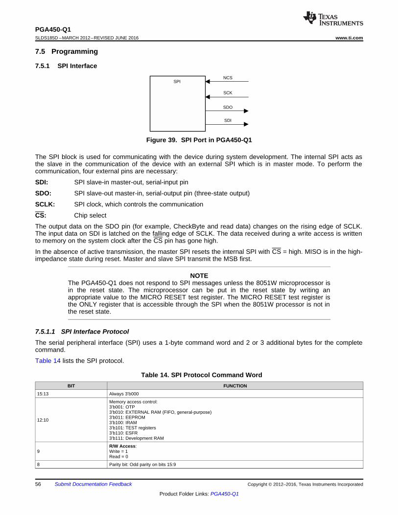
SPINCS
SCK
SDO
SDI
56
PGA450-Q1SLDS185D –MARCH 2012–REVISED JUNE 2016 www.ti.com
Product Folder Links: PGA450-Q1
Submit Documentation Feedback Copyright © 2012–2016, Texas Instruments Incorporated
7.5 Programming
7.5.1 SPI Interface
Figure 39. SPI Port in PGA450-Q1
The SPI block is used for communicating with the device during system development. The internal SPI acts asthe slave in the communication of the device with an external SPI which is in master mode. To perform thecommunication, four external pins are necessary:
SDI: SPI slave-in master-out, serial-input pin
SDO: SPI slave-out master-in, serial-output pin (three-state output)
SCLK: SPI clock, which controls the communication
CS: Chip select
The output data on the SDO pin (for example, CheckByte and read data) changes on the rising edge of SCLK.The input data on SDI is latched on the falling edge of SCLK. The data received during a write access is writtento memory on the system clock after the CS pin has gone high.
In the absence of active transmission, the master SPI resets the internal SPI with CS = high. MISO is in the high-impedance state during reset. Master and slave SPI transmit the MSB first.
NOTEThe PGA450-Q1 does not respond to SPI messages unless the 8051W microprocessor isin the reset state. The microprocessor can be put in the reset state by writing anappropriate value to the MICRO RESET test register. The MICRO RESET test register isthe ONLY register that is accessible through the SPI when the 8051W processor is not inthe reset state.
7.5.1.1 SPI Interface ProtocolThe serial peripheral interface (SPI) uses a 1-byte command word and 2 or 3 additional bytes for the completecommand.
Table 14 lists the SPI protocol.
Table 14. SPI Protocol Command WordBIT FUNCTION
15:13 Always 3’b000
12:10
Memory access control:3’b001: OTP3’b010: EXTERNAL RAM (FIFO, general-purpose)3’b011: EEPROM3’b100: IRAM3’b101: TEST registers3’b110: ESFR3’b111: Development RAM
9R/W Access:Write = 1Read = 0
8 Parity bit: Odd parity on bits 15:9

SPI Read Command 1
Response from the PGA450-Q1 device for
Read Command 1
SPI Read Command 2
Response from the PGA450-Q1 device for
Read Command 2
Time
SPI Read Command 3
57
PGA450-Q1www.ti.com SLDS185D –MARCH 2012–REVISED JUNE 2016
Product Folder Links: PGA450-Q1
Submit Documentation FeedbackCopyright © 2012–2016, Texas Instruments Incorporated
When accessing memory (IRAM, ESFR, OTP, EEPROM, FIFO RAM, DEV RAM), the internal registers bits 15:13must all be zero. If these bits are not zero, the SPI command is rejected and the SPI failure bit is set (seeCheckByte below).
7.5.1.2 Transfer WidthTable 15 lists how the SPI transfer width (number of bytes) varies depending on whether the SPI is a read orwrite to the IRAM, ESFR, EEPROM, OTP, or FIFO data access.
Table 15. SPI Protocol Transfer WidthsMEMORY ACCESS
MODEREG
ACCESSMEMORYACCESS R/W PARITY
BITTYPE OF
OPERATION ADDRESS DATA DATA TOTAL NO.OF BYTES
Byte #1 (Breakdown) Bytes
Bits 7:5 Bits 4:2 Bit 1 Bit 0 Byte #1 (Hex) Byte #2 Byte #3 Byte #4
Internal RAM write 000 100 1 1 13 8-bit RAMAddress 8-bit Write Data — 3
Internal RAM read 000 100 0 0 10 8-bit RAMAddress 8-bit Don't Care — 3
ESFR write 000 110 1 0 1A 8-bit ESFRAddress 8-bit Write Data — 3
ESFR read 000 110 0 1 19 8-bit ESFRAddress 8-bit Don't Care — 3
OTP write 000 001 1 1 07 OTP Address15:8
OTP Address7:0 8-bit write data 4
OTP read 000 001 0 0 04 OTP Address15:8
OTP Address7:0 8-bit don't care 4
EEPROM cache write 000 011 1 0 0E 8-bit EEPROMAddress 8-bit Write Data — 3
EEPROM cache read 000 011 0 1 0D 8-bit EEPROMAddress 8-bit Don't Care — 3
External RAM write 000 010 1 1 0BEXTERNALRAM Address15:8
EXTERNALAddress 7:0 8-bit write data 4
External RAM read 000 010 0 0 08 EXTERNALAddress 15:8
EXTERNALAddress 7:0 8-bit don't care 3
DEV RAM write 000 111 1 1 1F DEV RAMAddress 15:8
DEV RAMAddress 7:0 8-bit write data 4
DEV RAM read 000 111 0 0 1C DEV RAMAddress 15:8
DEV RAMAddress 7:0 8-bit don't care 4
TEST write 000 101 1 0 16 8-bit TESTAddress 8-bit Write Data — 3
TEST read 000 101 0 1 15 8-bit TESTAddress 8-bit Don't Care — 3
For a SPI transfer to the internal register file, the parity P depends on the address.
For SPI transfers to the memories (IRAM, ESFR, OTP), the read data is available on the next SPI transfer. Thatis, when reading from a memory location, the user must send a subsequent transfer to get the data back.
Figure 40. Response to SPI Read Commands Is Available When the Next Command Is Sent

SPI Read Command 1
CheckByte
SPI Read Command 2
Data
Time
Response from PGA450-Q1 for Read Command 1
15 8 7 0
58
PGA450-Q1SLDS185D –MARCH 2012–REVISED JUNE 2016 www.ti.com
Product Folder Links: PGA450-Q1
Submit Documentation Feedback Copyright © 2012–2016, Texas Instruments Incorporated
7.5.1.3 CheckByteOn every SPI transfer, the PGA450-Q1 transmits a CheckByte which is in the 8 most significant bits of thetransfer. For example, in a 16-bit transfer, the CheckByte is in bits 15:8 of the received data; similarly, for a 24 bittransfer the CheckByte is in bits 23:16 of the received data. The CheckByte can be used by the SPI master todetect SPI communication errors.
Figure 41. CheckByte Is Transmitted by PGA450-Q1 at the Beginning of Every Response
Table 16 lists the interpretation of each bit in the CheckByte transmitted by the PGA450-Q1.
For a successful SPI transfer, the CheckByte reads 8’h02. Bit 9 of the CheckByte is always set in order to assistdebugging in the lab. If the SPI transfer failed for some reason, the most significant bit (15) of the CheckByte isset. The reason for the failure is then described in bits 14:11.
Table 16. SPI Protocol, CheckByte FieldCheckByte BIT ERROR DESCRIPTION
15 (or most significant bit) SPI transfer failure SPI transfer failure14 Parity error Parity error; command-byte parity incorrect13 Illegal address Illegal address; bits 15:13 and 12:10 cannot both be active12 Illegal command Illegal command; memory access bits 12:10 invalid11 Wrong number of clocks Wrong number clocks; must only receive 16, 24, or 32 clocks10:8 Always 3’b010 Always 3’b010
7.5.1.4 ExamplesTable 17 lists a few examples of SPI transfer:
Table 17. SPI Protocol ExamplesCOMMAND SPI SLAVE TRANSFER
Read internal register 0 (revision id) ({3’h0, 3’h0, 1’b0, 1’b1}, 8’hXX)Write 0x80 to internal register 1 (MicroConfig) ({3’h1, 3’h0, 1’b1, 1’b1}, 8’hC8)Write 0x34 to internal RAM 0x7F ({3’h0, 3’h4, 1’b1, 1’b1}, 8’h7F, 8’h34)Read from ESFR 0xC0 ({3’h0, 3’h6, 1’b0, 1’b1}, 8’hC0)Write 0xD9 to OTP 0x1765 ({3’h0, 3’h1, 1’b1, 1’b1}, 8’h17, 8’h65, 8’hD9)Failed write 0xC8 to internal register 1 (bad parity) ({3’h1, 3’h0, 1’b1, 1’b0}, 8’hC8)Failed write 0xC8 to internal register 1 (illegal address) ({3’h1, 3’h1, 1’b1, 1’b0}, 8’hC8)Failed write 0x34 to memory (illegal command) ({3’h0, 3’h7, 1’b1, 1’b1}, 8’h7F, 8’h34)
7.5.2 Diagnostics
7.5.2.1 Power-Block MonitorsThe following operating-condition monitors have been implemented on the PGA450-Q1 to ensure reliable androbust performance over the lifetime of the device.• VPWR overvoltage (greater than 28 V nominal, 20-µs deglitch time)• VPWR level is such that AVDD is undervoltage (less than 6 V nominal, 2-ms deglitch time)
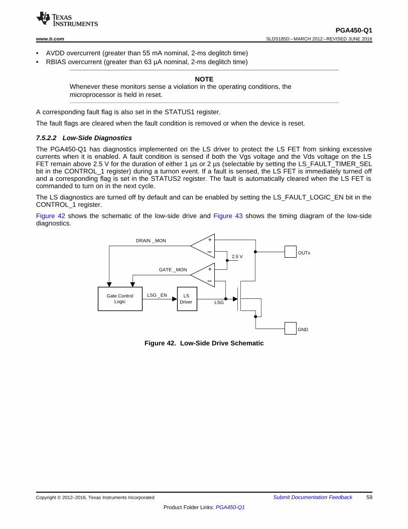
Gate Control Logic
2.5 VOUTx
GND
LS Driver
DRAIN _MON
GATE _MON
LSG _EN
LSG
+
+
59
PGA450-Q1www.ti.com SLDS185D –MARCH 2012–REVISED JUNE 2016
Product Folder Links: PGA450-Q1
Submit Documentation FeedbackCopyright © 2012–2016, Texas Instruments Incorporated
• AVDD overcurrent (greater than 55 mA nominal, 2-ms deglitch time)• RBIAS overcurrent (greater than 63 µA nominal, 2-ms deglitch time)
NOTEWhenever these monitors sense a violation in the operating conditions, themicroprocessor is held in reset.
A corresponding fault flag is also set in the STATUS1 register.
The fault flags are cleared when the fault condition is removed or when the device is reset.
7.5.2.2 Low-Side DiagnosticsThe PGA450-Q1 has diagnostics implemented on the LS driver to protect the LS FET from sinking excessivecurrents when it is enabled. A fault condition is sensed if both the Vgs voltage and the Vds voltage on the LSFET remain above 2.5 V for the duration of either 1 µs or 2 µs (selectable by setting the LS_FAULT_TIMER_SELbit in the CONTROL_1 register) during a turnon event. If a fault is sensed, the LS FET is immediately turned offand a corresponding flag is set in the STATUS2 register. The fault is automatically cleared when the LS FET iscommanded to turn on in the next cycle.
The LS diagnostics are turned off by default and can be enabled by setting the LS_FAULT_LOGIC_EN bit in theCONTROL_1 register.
Figure 42 shows the schematic of the low-side drive and Figure 43 shows the timing diagram of the low-sidediagnostics.
Figure 42. Low-Side Drive Schematic

GATE_EN
GATE
DRAIN
GATE_MON
DRAIN_MON
See note A Seenote B
Seenote C
See note D
Fau
lt tim
e
Fault condition
60
PGA450-Q1SLDS185D –MARCH 2012–REVISED JUNE 2016 www.ti.com
Product Folder Links: PGA450-Q1
Submit Documentation Feedback Copyright © 2012–2016, Texas Instruments Incorporated
A. Gate is commanded on by LS driver logic. This 0 -> 1 edge enables the LS fault diagnostic on the LS Driver if theLS_FAULT_LOGIC_EN is set.
B. Drain monitor (DRAIN_MON) senses that drain is below 2.5 V for a normal scenario, where as the drain monitoroutput remains high for the fault scenario.
C. Gate monitor (GATE_MON) senses that gate is above 2.5 V.D. For the fault scenario, bcause GATE_MON and DRAIN_MON signals have remained high for the selected fault time
(1 µs or 2 µs), a fault is sensed and the gate is immediately turned off.
Figure 43. Low-Side Fault Timing
7.5.2.3 Main Oscillator WatchdogThe PGA450-Q1 implements an internal free-running 500-kHz watchdog clock. This watchdog clock is used tomonitor the internal 16-MHz main oscillator or the external crystal oscillator. When this frequency is outside thisrange, an internal reset is generated, which resets the entire digital core; this is equivalent to POR.
The main oscillator frequency fail limits have the following ranges as shown in Figure 44:• If the main oscillator frequency is less than 5.4 MHz, the watchdog logic recognizes this as a low-frequency
fail and resets the digital core.• If the main oscillator frequency lies in the range: 5.4 MHz < Main OSC Freq < 14 MHz, there is a possibility
that the watchdog recognizes this as a low-frequency fail and resets the core, but reset is not assured.• If the main oscillator frequency lies in the range: 14 MHz < Main Osc Freq < 18 MHz, the main osc watchdog
does NOT reset the core, as this is seen as the nominal frequency of operation.• If the main oscillator frequency lies in the range 18 MHz < Main Osc Freq < 43 MHz, there is a possibility that
the watchdog recognizes this as a high-frequency fail and resets the core, but reset is not assured.• If the main oscillator frequency is greater than 43 MHz, the watchdog logic recognizes this as a high-
frequency fail and resets the digital core.

RESET
P3.7
8051W Software
Watchdog
5.4 MHZ 14 MHZ 18 MHZ 43 MHZ
NORMALMAY RESETRESET MAY RESET RESET
Main Oscillator Frequency
61
PGA450-Q1www.ti.com SLDS185D –MARCH 2012–REVISED JUNE 2016
Product Folder Links: PGA450-Q1
Submit Documentation FeedbackCopyright © 2012–2016, Texas Instruments Incorporated
Figure 44. Main Oscillator Frequency and the Corresponding PGA450-Q1 Behavior
The main oscillator watchdog can be disabled using the OSC_WD_EN bit in the WD_EN register.
NOTEA reset because of main oscillator watchdog failure causes an internal digital core reset.All ESFRs revert back to the reset sate.
7.5.2.4 Software WatchdogThe PGA450-Q1 implements a software watchdog. This watchdog must be serviced by software every 250 ms. Ifthe software does not service the watchdog within 250 ms of the last service, then the transducer drive FETs areturned OFF and the 8051W core is reset.
The software services the watchdog using port pin P3.7 as shown in Figure 45. The software services thewatchdog by toggling the state of P3.7.
Figure 45. Connection Between the 8051W and the Software Watchdog
The software watchdog can be disabled using the SW_WD_EN bit in the WD_EN register. The following lists thebehavior of this bit:• The SW_WD_EN bit is in the disabled state after power-on reset (POR).• If the 8051W is reset through the SPI, then SW_WD_EN is disabled.• If SW_WD_EN is enabled and the 8051W is reset because the software watchdog has timed out, then
SW_WD_EN remains enabled.
NOTEA reset of the 8051W does not change the state of the ESFR registers. The ESFRregisters continue to retain the state.

62
PGA450-Q1SLDS185D –MARCH 2012–REVISED JUNE 2016 www.ti.com
Product Folder Links: PGA450-Q1
Submit Documentation Feedback Copyright © 2012–2016, Texas Instruments Incorporated
7.5.2.5 Internal ASIC TRIM ValidityThe PGA450-Q1 has internal ASIC trim values. These trim values are used to fine-tune the operation of variousblocks at TI manufacturing EOL.
The PGA450-Q1 checks the validity of these ASIC trim values after power up and before the 8051W reset isdeasserted. If the internal trim values are not valid, the TRIM_FAIL bit in the STATUS1 register is set. The8051W software can be used to check this bit after 8051W reset is deasserted and the software starts execution.
7.5.2.6 FIFO RAM and External SRAM MBISTThe PGA450-Q1 verifies the integrity of FIFO RAM and RAM in the external memory space (that is, all RAM inthe external memory) with a RAM MBIST. The RAM MBIST begins immediately after POR is deasserted andtakes approximately 5 ms. See Figure 8 for power-up waveforms. The 8051W reset is deasserted while MBIST isongoing.
MBIST sets the MBIST_DONE flag in STATUS1 upon completion of MBIST. The MBIST_FLAG is set to 1 ifRAM MBIST fails.
NOTEThe 8051W microprocessor should not enable the digital datapath, should not access theFIFO RAM, and should not access RAM in the external memory space until the RAMMBIST DONE flag is set.
7.5.2.7 Thermal ShutdownThe PGA450-Q1 also has an overtemperature protection feature implemented. An overtemperature violationcauses a total shutdown of the part with the microprocessor held in reset. When the device cools down below theovertemperature threshold, the device initiates a power up again.

63
PGA450-Q1www.ti.com SLDS185D –MARCH 2012–REVISED JUNE 2016
Product Folder Links: PGA450-Q1
Submit Documentation FeedbackCopyright © 2012–2016, Texas Instruments Incorporated
7.5.3 8051W InterruptsThe MCU 8051 provides the five standard 8051-compatible legacy interrupts, plus expansion capability for afurther nine extended interrupts sourced from external user logic. The standard and extended interrupts eachhave separate enable-register bits associated with them, allowing software control. The interrupts can also havetwo levels of priority assigned to them. The interrupts are defined as follows:
Standard interrupts The five standard interrupts comprise two timer overflow interrupts, an interrupt associatedwith the built-in serial interface of the core, and two external interrupts (referred to as legacyexternal interrupts).
Timer-overflow interrupts The two timer-overflow interrupts, TF0 and TF1, are set whenever their respectivetimers timer 0 and timer 1, roll over to zero. The states of these interrupts are also stored in theTCON register. The TF0 and TF1 interrupts are automatically cleared by hardware on entry to thecorresponding interrupt service routine.
NOTEAll events on NINT0 and NINT1, whether level-triggered or edge-triggered, aredetected by sampling the relevant interrupt line on the rising edge of SCLK at theend of phase 1 of every machine cycle. Where NINT0/NINT1 is level-triggered, aresponse is made to the signal being sampled low and, to ensure detection, theexternal source must hold the line low until the resulting interrupt is generated. (Italso must ensure that the request is de-activated before the end of the associatedservice routine.) Where NINT0 or NINT1 is edge-triggered, the response is made toa transition on the signal from high to low between successive samples. Thismeans that, to ensure detection, NINT0 or NINT1 must have been high for at leasttwo clocks before it goes low and then must be held low for at least two clocks afterthis transition.
Serial interrupt The serial interrupts source comprises the logical OR of the two serial interface status bits RIand TI in register SCON. These interrupts are set automatically on receipt or transmission of a dataframe. These two bits are not cleared by hardware.
Legacy external interrupts The two legacy external interrupts, NINT0 and NINT1, are driven from inputsPORT3(2) and PORT3(3), respectively. These interrupts can be either edge- or level-sensitive,depending on settings within the TCON register. Two further TCON register bits, IE0 and IE1, actas interrupt flags. If the external interrupt is set to edge-triggered, the corresponding register bit IE0or IE1 is set by a falling edge on NINT0 or NINT1 and cleared by hardware on entry to thecorresponding interrupt service routine. If the interrupt is set to be level-sensitive, IE0or IE1 reflectsthe logic level on NINT0 or NINT1. The TCON register is described in the Timer and CounterControl Register (offset = 0x88) [reset = 0] section.
Extended interrupts Source and acknowledge signals are provided for a further nine interrupts. Theseinterrupts are driven from external user logic, typically a user ESFR. The extended interrupts areinput to the core on bits 5 to 13 of input bus XINTR_SRC, whereas acknowledge signals are outputfrom the core on bits 5 to 13 of bus XINTR_ACK. Note: If the timers or the UART are omitted fromthe design, their corresponding interrupt inputs (plus those of the legacy external interrupts wherethe timers are omitted) are made available at the core periphery as XINTR_SRC[4:0], along withcorresponding XINTR_ACK acknowledge signals, for use as additional extended interrupts.)I
The extended-interrupt lines are sampled on the rising edge of PCLK at the beginning of phase 2 of thelast cycle of the current instruction. To ensure detection, the external source must hold the XINTR_SRCline high until the resulting interrupt is generated and must also ensure that the request is deactivatedbefore the end of the associated service routine.IAny edge-triggering that is required must be taken care of by individual peripherals.

64
PGA450-Q1SLDS185D –MARCH 2012–REVISED JUNE 2016 www.ti.com
Product Folder Links: PGA450-Q1
Submit Documentation Feedback Copyright © 2012–2016, Texas Instruments Incorporated
NOTEFor additional information about these five standard interrupts, see the Intel 8-BitEmbedded Controller Handbook in the Hardware Description of the 8051, 8052 and80C51.)
7.5.3.1 Interrupt Flag ClearIf the legacy external interrupts, NINT0 and NINT1, are edge-triggered, the interrupt flag is cleared on vectoringto the service routine. If these interrupts are level-triggered, the flag is controlled by the external signal. Timerand counter flags are cleared on vectoring to the interrupt service routine, but the serial interrupt flag is notaffected by hardware. The serial interrupt flag should be cleared by software. Acknowledge signals are providedfor clearing any registers used to source the nine additional interrupts.
7.5.3.2 Priority Levels and Interrupt VectorsOne of two priority levels can be selected for each interrupt. An interrupt of high priority may interrupt the serviceroutine of a low-priority interrupt and, if two interrupts of different priority occur at the same time, the higher-levelinterrupt is serviced first. An interrupt cannot be interrupted by another interrupt of the same priority level. If twointerrupts of the same priority level occur simultaneously, a polling sequence is observed as listed in Table 18:
When an interrupt is serviced, a long call instruction is executed to one of the following locations, according tothe source of the interrupt as listed in Table 18.
Table 18. Interrupt Summary
8051W SOURCE PGA450-Q1 SOURCEVECTORADDRES
SPOLLING
SEQUENCE FLAG ENABLE PRIORITYCONTROL
External interrupt 0 LIN RX 0x0003 1 (highest) IE0 (TCON.1) EX0 (IE.0) PX0 (IP.0)
Timer and counter interrupt0 ← 0x000B 2 TF0 (TCON.5) ET0 (IE.1) PT0 (IP.1)
External interrupt 1 LIN ~RX 0x0013 3 IE1 (TCON.3) EX1 (IE.2) PX1 (IP.2)
Timer and counter interrupt1 ← 0x001B 4 TF1 (TCON.7) ET1 (IE.3) PT1 (IP.3)
Serial port 0 ← 0x0023 5RI_0(SCON0.0)TI_0(SCON0.1)
ES0 (IE.4) PS0 (IP.4)
External interrupt 5 LIN PID received 0x002B 6 — EI5 (IE.5) PI5 (IP.5)
External interrupt 6 LIN/SCI DATA received 0x0033 7 — EI6 (IE1.0) PI6 (IP1.0)
External interrupt 7 LIN/SCI data transmitcomplete 0x003B 8 — EI7 (IE1.1) PI7 (IP1.1)
External interrupt 8 LIN SYNC received 0x0043 9 — EI8 (IE1.2) PI8 (IP1.2)
External interrupt 9 0x004B 10 — EI9 (IE1.3) PI9 (IP1.3)
External interrupt 10 0x0053 11 — EI10 (IE14) P10 (IP1.4)
External interrupt 11 0x005B 12 — EI11 (IE1.5) P11 (IP1.5)
External interrupt 12 0x0063 13 — EI12 (IE1.6) P12 (IP16)
External interrupt 13 0x006B 14 (Lowest) — EI13 (IE1.7) P13 (IP.7)
7.5.3.3 Interrupt LatencyThe response time in a single interrupt system is between 3 and 9 machine cycles.
7.5.4 InstructionsThe M8051 Warp instruction set is listed in Table 20. The following sections outline some of the supportedfeatures.
7.5.4.1 Addressing ModesThe M8051 Warp provides a variety of addressing modes, which are outlined as follows.

65
PGA450-Q1www.ti.com SLDS185D –MARCH 2012–REVISED JUNE 2016
Product Folder Links: PGA450-Q1
Submit Documentation FeedbackCopyright © 2012–2016, Texas Instruments Incorporated
7.5.4.1.1 Direct Addressing
In direct addressing, the operand is specified by an 8-bit address field. Only internal data and SFRs can beaccessed using this mode.
7.5.4.1.2 Indirect Addressing
In indirect addressing, the operand is specified by an address contained in a register. Two registers (R0 and R1)from the current bank or the data pointer can be used for addressing in this mode. Both internal and externaldata memory can be indirectly addressed.
7.5.4.1.3 Register Addressing
In register addressing, the operand is specified by the top 3 bits of the opcode, which selects one of the currentbank of registers. Four banks of registers are available. The current bank is selected by bits 3 and 4 of the PSW.
7.5.4.1.4 Register Specific Addressing
Some instructions only operate on specific registers which is defined by the opcode. In particular, manyaccumulator operations and some stack pointer operations are defined in this manner.
7.5.4.1.5 Immediate Data
Instructions which use immediate data are 2 or 3 bytes long, and the immediate operand is stored in programmemory as part of the instruction.
7.5.4.1.6 Indexed Addressing
Only program memory can be addressed using indexed addressing. This memory is intended for simpleimplementation of look-up tables. A 16-bit base register (either the PC or the DPTR) is combined with an offsetstored in the accumulator to access data in program memory.
7.5.4.2 Arithmetic InstructionsThe M8051 Warp implements ADD, ADDC (add with carry), SUBB (subtract with borrow), INC (increment), andDEC (decrement) functions, which can be used in most addressing modes. There are three accumulator-specificinstructions, DA A (decimal adjust A), MUL AB (multiply A by B) and DIV AB (divide A by B).
7.5.4.3 Logical InstructionsThe M8051 Warp implements ANL (AND logical), ORL (OR logical), and XRL (exclusive-OR logical) functions,which again can be used in most addressing modes. Seven accumulator-specific instructions are available, CLRA (clear A), CPL A (complement A), RL A (rotate left A), RLC A (rotate left through carry A), RR A (rotate rightA), RRC A (rotate right through carry A), and SWAP A (swap nibbles of A).
7.5.4.4 Data Transfers
7.5.4.4.1 Internal Data Memory
Data can be moved from the accumulator to any internal data memory location, from any internal data memorylocation to the accumulator, and from any internal data memory location to any SFR or other internal datamemory location.
7.5.4.4.2 External Data Memory
Data can be moved from the accumulator to or from an external memory location in one of two addressingmodes. In 8-bit addressing mode, the external location is addressed by either R0 or R1; in 16-bit addressingmode, the location is addressed by the DPTR.

66
PGA450-Q1SLDS185D –MARCH 2012–REVISED JUNE 2016 www.ti.com
Product Folder Links: PGA450-Q1
Submit Documentation Feedback Copyright © 2012–2016, Texas Instruments Incorporated
7.5.4.5 Jump Instructions
7.5.4.5.1 Unconditional Jumps
Four sorts of unconditional jump instructions are available. Short jumps (SJMP) are relative jumps (limited to–128 to 127 bytes), long jumps (LJMP) are absolute 16-bit jumps, and absolute jumps (AJMP) are absolute 11-bit jumps (that is, within a 2K byte memory page). The last type is an indexed jump, JMP @A+DPTR, whichjumps to a location contained in the DPTR register, offset by a value stored in the accumulator.
7.5.4.5.2 Subroutine Calls and Returns
Only two sorts of subroutine call are available, ACALL and LCALL, which are absolute and long as previouslydescribed. Two return instructions are provided, RET and RETI. The latter is for interrupt service routines.
7.5.4.5.3 Conditional Jumps
Conditional jump instructions all use relative addressing and there fore are limited to the same –128- to 127-byterange as previously described.
7.5.4.6 Boolean InstructionsThe bit-addressable registers in both the direct and SFR space can be manipulated using Boolean instructions.Logical functions are available which use the carry flag and an addressable bit as the operands and eachaddressable bit can be set, cleared, or tested in a jump instruction.
7.5.4.7 FlagsTable 19 lists the instructions that affect the flags generated by the ALU.
Table 19. Flag Summary
INSTRUCTIONFLAG
INSTRUCTIONFLAG
C OV AC C OV ACADD ? ? ? CLRC 0
ADDC ? ? ? CPLC ?SUBB ? ? ? ANL C, bit ?MUL 0 ? ANL C, /bit ?DIV 0 ? ORL C, bit ?DA ? ORL C, /bit ?
RRC ? MOV C, bit ?RLC ? CJNE ?
SETB C 1
In Table 19, a 0 indicates that the flag is always cleared, a 1 indicates that the flag is always set, and a questionmark (?) indicates that the state of the flag depends on the result of the operation. The flag specified as blankmeans that the state is unknown.
7.5.4.8 Instruction TableInstructions are either 1, 2, or 3 bytes long as listed in the BYTES column of Table 20. Each instruction requireseither 1, 2 or 4 machine cycles to execute as listed in Table 20. One machine cycle comprises 2 CCLK clockcycles.
Table 20. InstructionsMNEMONIC DESCRIPTION BYTES CYCLES HEX CODEARITHMETICADD A,Rn Add register to A 1 1 28–2FADD A,dir Add direct byte to A 2 1 25ADD A,@Ri Add indirect memory to A 1 1 26–27ADD A,#data Add immediate to A 2 1 24

67
PGA450-Q1www.ti.com SLDS185D –MARCH 2012–REVISED JUNE 2016
Product Folder Links: PGA450-Q1
Submit Documentation FeedbackCopyright © 2012–2016, Texas Instruments Incorporated
Table 20. Instructions (continued)MNEMONIC DESCRIPTION BYTES CYCLES HEX CODEADDC A,Rn Add register to A with carry 1 1 38–3FADDC A,dir Add direct byte to A with carry 2 1 35ADDC A,@Ri Add indirect memory to A with carry 1 1 36–37ADDC A,#data Add immediate to A with carry 2 1 34SUBB A,Rn Subtract register from A with borrow 1 1 98–9FSUBB A,dir Subtract direct byte from A with borrow 2 1 95SUBB A,@Ri Subtract indirect memory from A with borrow 1 1 96–97SUBB A,#data Subtract immediate from A with borrowINC A Increment A 1 1 4INC Rn Increment register 1 1 08–0FINC dir Increment direct byte 2 1 5INC @Ri Increment indirect memory 1 1 06-07DEC A Decrement A 1 1 14DEC Rn Decrement register 1 1 18–1FDEC dir Decrement direct byte 2 1 15DEC @Ri Decrement indirect memory 1 1 16–17INC DPTR Increment data pointer 1 2 A3MUL AB Multiply A by B 1 4 A4DIV AB Divide A by B 1 4 84DA A Decimal Adjust A 1 1 D4LOGICALANL A,Rn AND register to A 1 1 58–5FANL A,dir AND direct byte to A 2 1 55ANL A,@Ri AND indirect memory to A 1 1 56–57ANL A,#data AND immediate to A 2 1 54ANL dir,A AND A to direct byte 2 1 52ANL dir,#data AND immediate to direct byte 3 2 53ORL A,Rn OR register to A 1 1 48–4FORL A,dir OR direct byte to A 2 1 45ORL A,@Ri OR indirect memory to A 1 1 46–47ORL A,#data OR immediate to A 2 1 44ORL dir,A OR A to direct byte 2 1 42ORL dir,#data OR immediate to direct byte 3 2 43XRL A,Rn Exclusive-OR register to A 1 1 68–6FXRL A,dir Exclusive-OR direct byte to A 2 1 65XRL A, @Ri Exclusive-OR indirect memory to A 1 1 66–67XRL A,#data Exclusive-OR immediate to A 2 1 64XRL dir,A Exclusive-OR A to direct byte 2 1 62XRL dir,#data Exclusive-OR immediate to direct byte 3 2 63CLR A Clear A 1 1 E4CPL A Complement A 1 1 F4SWAP A Swap Nibbles of A 1 1 C4RL A Rotate A left 1 1 23RLC A Rotate A left through carry 1 1 33RR A Rotate A right 1 1 3RRC A Rotate A right through carry 1 1 13

68
PGA450-Q1SLDS185D –MARCH 2012–REVISED JUNE 2016 www.ti.com
Product Folder Links: PGA450-Q1
Submit Documentation Feedback Copyright © 2012–2016, Texas Instruments Incorporated
Table 20. Instructions (continued)MNEMONIC DESCRIPTION BYTES CYCLES HEX CODEDATA TRANSFERMOV A,Rn Move register to A 1 1 E8–EFMOV A,dir Move direct byte to A 2 1 E5MOV A,@Ri Move indirect memory to A 1 1 E6–E7MOV A,#data Move immediate to A 2 1 74MOV Rn,A Move A to register 1 1 F8–FFMOV Rn,dir Move direct byte to register 2 2 A8–AFMOV Rn,#data Move immediate to register 2 1 78–7FMOV dir,A Move A to direct byte 2 1 F5MOV dir,Rn Move register to direct byte 2 2 88–8FMOV dir,dir Move direct byte to direct byte 3 2 85MOV dir,@Ri Move indirect memory to direct byte 2 2 86–87MOV dir,#data Move immediate to direct byte 3 2 75MOV @Ri,A Move A to indirect memory 1 1 F6–F7MOV @Ri,dir Move direct byte to indirect memory 2 2 A6–A7MOV @Ri,#data Move immediate to indirect memory 2 1 76–77MOV DPTR,#data Move immediate to data pointer 3 2 90MOVC A,@A+DPTR Move code byte relative DPTR to A 1 2 93MOVC A,@A+PC Move code byte relative PC to A 1 2 83MOVX A,@Ri Move external data(A8) to A 1 2 E2–E3MOVX A,@DPTR Move external data(A16) to A 1 2 E0MOVX @Ri,A Move A to external data(A8) 1 2 F2–F3MOVX @DPTR,A Move A to external data(A16) 1 2 F0PUSH dir Push direct byte onto stack 2 2 C0POP dir Pop direct byte from stack 2 2 D0XCH A,Rn Exchange A and register 1 1 C8–CFXCH A,dir Exchange A and direct byte 2 1 C5XCH A,@Ri Exchange A and indirect memory 1 1 C6–C7XCHD A,@Ri Exchange A and indirect memory nibble 1 1 D6–D7BOOLEANCLR C Clear carry 1 1 C3CLR bit Clear direct bit 2 1 C2SETB C Set carry 1 1 D3SETB bit Set direct bit 2 1 D2CPL C Complement carry 1 1 B3CPL bit Complement direct bit 2 1 B2ANL C,bit AND direct bit to carry 2 2 82ANL C,/bit AND direct bit inverse to carry 2 2 B0ORL C,bit OR direct bit to carry 2 2 72ORL C,/bit OR direct bit inverse to carry 2 2 A0MOV C,bit Move direct bit to carry 2 1 A2MOV bit,C Move carry to direct bit 2 2 92BRANCHINGACALL addr 11 Absolute jump to subroutine 2 2 11→F1LCALL addr 16 Long jump to subroutine 3 2 12RET Return from subroutine 1 2 22RETI Return from interrupt 1 2 32

69
PGA450-Q1www.ti.com SLDS185D –MARCH 2012–REVISED JUNE 2016
Product Folder Links: PGA450-Q1
Submit Documentation FeedbackCopyright © 2012–2016, Texas Instruments Incorporated
Table 20. Instructions (continued)MNEMONIC DESCRIPTION BYTES CYCLES HEX CODEAJMP addr 11 Absolute jump unconditional 2 2 01→E1LJMP addr 16 Long jump unconditional 3 2 2SJMP rel Short jump (relative address) 2 2 80JC rel Jump on carry = 1 2 2 40JNC rel Jump on carry = 0 2 2 50JB bit,rel Jump on direct bit = 1 3 2 20JNB bit,rel Jump on direct bit = 0 3 2 30JBC bit,rel Jump on direct bit = 1 and clear 3 2 10JMP @A+DPTR Jump indirect relative DPTR 1 2 73JZ rel Jump on accumulator = 0 2 2 60JNZ rel Jump on accumulator ≠ 0 2 2 70CJNE A,dir,rel Compare A,direct jne relative 3 2 B5CJNE A,#d,rel Compare A,immediate jne relative 3 2 B4CJNE Rn,#d,rel Compare register, immediate jne relative 3 2 B8–BFCJNE @Ri,#d,rel Compare indirect, immediate jne relative 3 2 B6–B7DJNZ Rn,rel Decrement register, jnz relative 2 2 D8–DFDJNZ dir,rel Decrement direct byte, jnz relative 3 2 D5MISCELLANEOUSNOP No operation 1 1 0
In Table 20, an entry such as E8–EF indicates a continuous block of hex opcodes used for 8 different registers,the register numbers of which are defined by the lowest three bits of the corresponding code. Non-continuousblocks of codes, shown as 11→F1 (for example), are used for absolute jumps and calls, with the top 3 bits of thecode being used to store the top three bits of the destination address.
The CJNE instructions use the abbreviation #d for immediate data; other instructions use #data.
7.5.5 8051W Port UsageThe 8051W has four I/O ports. lists the port usage in the PGA450-Q1 device.
Table 21. 8051W I/O Port Usage in PGA450-Q1PORT BIT USAGE IN PGA450-Q1Port 0 0 OTP security
1 OTP security2 OTP security3 OTP security4 OTP security5 OTP security6 OTP security7 OTP security
Port 1 01234567
Port 2 0 Low side A

OTP ProgramCode Area
Program CodeMemory
Not Implemented
BANK3: R7-R0
Bit-Addressable
GeneralPurpose (RAM)
Internal DataMemory
SFRs
FIFO RAM
ExternalMemory
Not Implemented
EEPROM
Development RAMProgram Code
Area
RAM
GeneralPurpose (RAM)
Direct addressingSFRs and ESFRs
0x0000
0x02FF
0x0400
0x041F
0x03FF
0x0300
0xFFFF0xFF
0xF7
0xEF
0xE7
0xDF
0xD7
0xCF
0xC7
0xBF
0xB7
0xAF
0xA7
0x9F
0x97
0x8F
0x87
0x7F
0x77
0x6F
0x67
0x5F
0x57
0x4F
0x47
0x3F
0x37
0x2F
0x27
0x1F
0x17
0x0F
0x07
0xF8
0xF0
0xE8
0xE0
0xD8
0xD0
0xC8
0xC0
0xB8
0xB0
0xA8
0xA0
0x98
0x90
0x88
0x80
0x78
0x70
0x68
0x60
0x58
0x50
0x48
0x40
0x38
0x30
0x28
0x20
0x18
0x10
0x08
0x00
BANK2: R7-R0
BANK1: R7-R0
BANK0: R7-R0
0xFFFF
0x3FFF
0x2000
0x1FFF
0x0000
70
PGA450-Q1SLDS185D –MARCH 2012–REVISED JUNE 2016 www.ti.com
Product Folder Links: PGA450-Q1
Submit Documentation Feedback Copyright © 2012–2016, Texas Instruments Incorporated
Table 21. 8051W I/O Port Usage in PGA450-Q1 (continued)PORT BIT USAGE IN PGA450-Q1
1 Low side B23 LIN Tx4567
Port 3 0 UART RxD1 UART TxD2 LIN Rx/external interrupt input 0, active-low3 ~LIN Rx/external interrupt input 1, active-low4 GPIO1/Timer 0 external input5 GPIO2/Timer 1 external input67 Software watchdog
7.6 Register MapsThe memory block consists of SRAM, OTP, and EEPROM. The SRAM is used as storage for volatile softwarevariables during program execution. The OTP consists of the program code and the EEPROM consists ofcalibrations.
Figure 46. PGA450 Memory Map

PGA450-Q1www.ti.com SLDS185D –MARCH 2012–REVISED JUNE 2016
71
Product Folder Links: PGA450-Q1
Submit Documentation FeedbackCopyright © 2012–2016, Texas Instruments Incorporated
Table 22. SFR Memory MapAddress (hex) Description D6 D5 D4 D3 D2 D1 D0 R/W POWER ON Value
80 Port 0 (P0) P0[6] P0[5] P0[4] P0[3] P0[2] P0[1] P0[0] R/W 0xFF
81 Stack Pointer SP[6] SP[5] SP[4] SP[3] SP[2] SP[1] SP[0] R/W 0
82 Data Pointer Low Byte DPTR[6] DPTR[5] DPTR[4] DPTR[3] DPTR[2] DPTR[1] DPTR[0] R/W 0
83 Data Pointer High Byte DPTR[14] DPTR[13] DPTR[12] DPTR[11] DPTR[10] DPTR[9] DPTR[8] R/W 0
87 Power control Register GF1 GF0 PD IDL R/W 0
88 Timer / Counter Control TR1 TF0 TR0 IE1 IT1 IE0 IT0 R/W 0
89 Timer / Counter Mode CNT1 M1 (1) M0 (1) GATE0 CNT0 M1 (0) M0 (0) R/W 0
8A Timer / Counter Data (TL0) TL0[6] TL0[5] TL0[4] TL0[3] TL0[2] TL0[1] TL0[0] R/W 0
8B Timer / Counter Data (TL1) TL1[6] TL1[5] TL1[4] TL1[3] TL1[2] TL1[1] TL1[0] R/W 0
8C Timer / Counter Data (TH0) TH0[6] TH0[5] TH0[4] TH0[3] TH0[2] TH0[1] TH0[0] R/W 0
8D Timer / Counter Data (TH1) TH1[6] TH1[5] TH1[4] TH1[3] TH1[2] TH1[1] TH1[0] R/W 0
90 Port 1 (P1) P1[6] P1[5] P1[4] P1[3] P1[2] P1[1] P1[0] R/W 0xFF
98 UART Control (SCON) SM1 SM2 REN TB8 RB8 TI RI R/W 0
99 UART Data (SBUF) SBUF[6] SBUF[5] SBUF[4] SBUF[3] SBUF[2] SBUF[1] SBUF[0] R/W 0
A0 Port 2 (P2) P2[6] P2[5] P2[4] P2[3] P2[2] P2[1] P2[0] R/W 0xFF
A8 Interrupt Enable Register 0 EI5 ES ET1 EX1 ET0 EX0 R/W 0
B0 Port 3 (P3) P3[6] P3[5] P3[4] P3[3] P3[2] P3[1] P3[0] R/W 0xFF
B8 Interrupt Priority Register 0 PI5 PS PT1 PX1 PT0 PX0 R/W 0
D0 Program Status Word AC F0 RS1 RS0 OV F1 P R/W 0
E0 Accumulator ACC[6] ACC[5] ACC[4] ACC[3] ACC[2] ACC[1] ACC[0] R/W 0
E8 Interrupt Enable Register 1 EI12 EI11 EI10 EI9 EI8 EI7 EI6 R/W 0
F0 Register (B) B[6] B[5] B[4] B[3] B[2] B[1] B[0] R/W 0
F8 Interrupt Priority Register 1 PI12 PI11 PI10 PI9 PI8 PI7 PI6 R/W 0

PGA450-Q1SLDS185D –MARCH 2012–REVISED JUNE 2016 www.ti.com
72
Product Folder Links: PGA450-Q1
Submit Documentation Feedback Copyright © 2012–2016, Texas Instruments Incorporated
Table 23. ESFR Memory MapAddress (hex) D7 D6 D5 D4 D3 D2 D1 D0 R/W Power Up Description (Programmable
Regs)
92 BPF_B1[15] BPF_B114] BPF_B1[13] BPF_B1[12] BPF_B1[11] BPF_B1[10] BPF_B1[9] BPF_B1[8] R/W 0 BPF_B1_MSB
93 BPF_B1[7] BPF_B1[6] BPF_B1[5] BPF_B1[4] BPF_B1[3] BPF_B1[2] BPF_B1[1] BPF_B1[0] R/W 0 BPF_B1_LSB
94 BPF_A2[15] BPF_A2[14] BPF_A2[13] BPF_A2[12] BPF_A2[11] BPF_A2[10] BPF_A2[9] BPF_A2[8] R/W 0 BPF_A2_MSB
95 BPF_A2[7] BPF_A2[6] BPF_A2[5] BPF_A2[4] BPF_A2[3] BPF_A2[2] BPF_A2[1] BPF_A2[0] R/W 0 BPF_A2_LSB
96 BPF_A3[15] BPF_A3[14] BPF_A3[13] BPF_A3[12] BPF_A3[11] BPF_A3[10] BPF_A3[9] BPF_A3[8] R/W 0 BPF_A3_MSB
97 BPF_A3[7] BPF_A3[6] BPF_A3[5] BPF_A3[4] BPF_A3[3] BPF_A3[2] BPF_A3[1] BPF_A3[0] R/W 0 BPF_A3_LSB
A1 LPF_B1[14] LPF_B1[13] LPF_B1[12] LPF_B1[11] LPF_B1[10] LPF_B1[9] LPF_B1[8] R/W 0 LPF_B1_MSB
A2 LPF_B1[7] LPF_B1[6] LPF_B1[5] LPF_B1[4] LPF_B1[3] LPF_B1[2] LPF_B1[1] LPF_B1[0] R/W 0 LPF_B1_LSB
A3 LPF_A2[14] LPF_A2[13] LPF_A2[12] LPF_A2[11] LPF_A2[10] LPF_A2[9] LPF_A2[8] R/W 0 LPF_A2_MSB
A4 LPF_A2[7] LPF_A2[6] LPF_A2[5] LPF_A2[4] LPF_A2[3] LPF_A2[2] LPF_A2[1] LPF_A2[0] R/W 0 LPF_A2_LSB
A5 DS5 DS4 DS3 DS2 DS1 DS0 R/W 0 DOWNSAMPLE
A6 ONA[10] ONA[9] ONA[8] R/W 0 ONA_MSB
A7 ONA[7] ONA[6] ONA[5] ONA[4] ONA[3] ONA[2] ONA[1] ONA[0] R/W 0 ONA_LSB
A9 OFFA[10] OFFA[9] OFFA[8] R/W 0 OFFA_MSB
AA OFFA[7] OFFA[6] OFFA[5] OFFA[4] OFFA[3] OFFA[2] OFFA[1] OFFA[0] R/W 0 OFFA_LSB
AB ONB[10] ONB[9] ONB[8] R/W 0 ONB_MSB
AC ONB[7] ONB[6] ONB[5] ONB[4] ONB[3] ONB[2] ONB[1] ONB[0] R/W 0 ONB_LSB
AD OFFB[10] OFFB[9] OFFB[8] R/W 0 OFFB_MSB
AE OFFB[7] OFFB[6] OFFB[5] OFFB[4] OFFB[3] OFFB[2] OFFB[1] OFFB[0] R/W 0 OFFB_LSB
AF PCA5 PCA4 PCA3 PCA2 PCA1 PCA0 R/W 0 PULSE_CNTA
B1 PCB5 PCB4 PCB3 PCB2 PCB1 PCB0 R/W 0 PULSE_CNTB
B2 DT7 DT6 DT5 DT4 DT3 DT2 DT1 DT0 R/W 0 DEADTIME
B3 BMODE2 BMODE1 BMODE0 R/W 0 BURST_MODE
B4 TS7 TS6 TS5 TS4 TS3 TS2 TS1 TS0 R 0 TEMP_SENS
B5 SD7 SD6 SD5 SD4 SD3 SD2 SD1 SD0 R/W 0 SAT_DEGLITCH
B6 ST7 ST6 ST5 ST4 ST3 ST2 ST1 ST0 R 0 SAT_TIME
B7 LS_FAULT_LOGIC_EN
LS_FAULT_TIMER_SEL LNA_GAIN1 LNA_GAIN0 SAT_SEL1 SAT_SEL0 R/W 0 CONTROL_1
B9 BT7 BT6 BT5 BT4 BT3 BT2 BT1 BT0 R/W 0 BLANKING_TIMER
BA FRT[15] FRT[14] FRT[13] FRT[12] FRT[11] FRT[10] FRT[9] FRT[8] R 0 FRT_MSB
BB FRT[7] FRT[6] FRT[5] FRT[4] FRT[3] FRT[2] FRT[1] FRT[0] R 0 FRT_LSB
BC MICRO_LIN_TX UARTTX_CONFIG
GPIO2_CONFIG2
GPIO2_CONFIG1
GPIO2_CONFIG0
GPIO1_CONFIG2
GPIO1_CONFIG1
GPIO1_CONFIG0 R/W 0 GPIO_CTRL
BD CLK_SEL1 CLK_SEL0 R/W 0 CLK_SEL
BE SW_WD_EN OSC_WD_EN R/W 0 WD_EN
BF LIN_SCI R/W 0 LIN_SCI
C0 RELOAD WRITE/EE_STATUS R/W 0 EE_CTRL
C1 TRIM_FAIL MBIST_DONE MBIST_FAIL VPWR_OV AVDD_UV AVDD_OC RBIAS_OC R N/A STATUS1
C2 WD_TO_OSC LSB_FAULT LSA_FAULT WD_TO_SW SAT_DONE VREG_READY R N/A STATUS2

PGA450-Q1www.ti.com SLDS185D –MARCH 2012–REVISED JUNE 2016
73
Product Folder Links: PGA450-Q1
Submit Documentation FeedbackCopyright © 2012–2016, Texas Instruments Incorporated
Table 23. ESFR Memory Map (continued)Address (hex) D7 D6 D5 D4 D3 D2 D1 D0 R/W Power Up Description (Programmable
Regs)
C3 VREG_EN ACTIVE_EN R/W 0 PWR_MODE
C4 FIFO_ADC SCI_TX_EN FIFO_PEAKDET R/W 0 DP_SCI_CTRL
C5 NROLLOVER FMODE1 FMODE0 R/W 0 FIFO_CTRL
C8 CAP_FR_TIMER ECHO_EN SAT_EN BURST_B_EN BURST_EN R N/A EN_CTRL
C9 RX_DATA1[7] RX_DATA1[6] RX_DATA1[5] RX_DATA1[4] RX_DATA1[3] RX_DATA1[2] RX_DATA1[1] RX_DATA1[0] R N/A RX_DATA1
CA RX_DATA2[7] RX_DATA2[6] RX_DATA2[5] RX_DATA2[4] RX_DATA2[3] RX_DATA2[2] RX_DATA2[1] RX_DATA2[0] R N/A RX_DATA2
CB RX_DATA3[7] RX_DATA3[6] RX_DATA3[5] RX_DATA3[4] RX_DATA3[3] RX_DATA3[2] RX_DATA3[1] RX_DATA3[0] R N/A RX_DATA3
CC RX_DATA4[7] RX_DATA4[6] RX_DATA4[5] RX_DATA4[4] RX_DATA4[3] RX_DATA4[2] RX_DATA4[1] RX_DATA4[0] R N/A RX_DATA4
CD RX_DATA5[7] RX_DATA5[6] RX_DATA5[5] RX_DATA5[4] RX_DATA5[3] RX_DATA5[2] RX_DATA5[1] RX_DATA5[0] R N/A RX_DATA5
CE RX_DATA6[7] RX_DATA6[6] RX_DATA6[5] RX_DATA6[4] RX_DATA6[3] RX_DATA6[2] RX_DATA6[1] RX_DATA6[0] R N/A RX_DATA6
CF RX_DATA7[7] RX_DATA7[6] RX_DATA7[5] RX_DATA7[4] RX_DATA7[3] RX_DATA7[2] RX_DATA7[1] RX_DATA7[0] R N/A RX_DATA7
D1 RX_DATA8[7] RX_DATA8[6] RX_DATA8[5] RX_DATA8[4] RX_DATA8[3] RX_DATA8[2] RX_DATA8[1] RX_DATA8[0] R N/A RX_DATA8
D2 PID7 PID6 PID5 PID4 PID3 PID2 PID1 PID0 R N/A LIN_PID
D3 TX_DATA1[7] TX_DATA1[6] TX_DATA1[5] TX_DATA1[4] TX_DATA1[3] TX_DATA1[2] TX_DATA1[1] TX_DATA1[0] R/W N/A TX_DATA1
D4 TX_DATA2[7] TX_DATA2[6] TX_DATA2[5] TX_DATA2[4] TX_DATA2[3] TX_DATA2[2] TX_DATA2[1] TX_DATA2[0] R/W N/A TX_DATA2
D5 TX_DATA3[7] TX_DATA3[6] TX_DATA3[5] TX_DATA3[4] TX_DATA3[3] TX_DATA3[2] TX_DATA3[1] TX_DATA3[0] R/W N/A TX_DATA3
D6 TX_DATA4[7] TX_DATA4[6] TX_DATA4[5] TX_DATA4[4] TX_DATA4[3] TX_DATA4[2] TX_DATA4[1] TX_DATA4[0] R/W N/A TX_DATA4
D7 TX_DATA5[7] TX_DATA5[6] TX_DATA5[5] TX_DATA5[4] TX_DATA5[3] TX_DATA5[2] TX_DATA5[1] TX_DATA5[0] R/W N/A TX_DATA5
D8 TX_DATA6[7] TX_DATA6[6] TX_DATA6[5] TX_DATA6[4] TX_DATA6[3] TX_DATA6[2] TX_DATA6[1] TX_DATA6[0] R/W N/A TX_DATA6
D9 TX_DATA7[7] TX_DATA7[6] TX_DATA7[5] TX_DATA7[4] TX_DATA7[3] TX_DATA7[2] TX_DATA7[1] TX_DATA7[0] R/W N/A TX_DATA7
DA TX_DATA8[7] TX_DATA8[6] TX_DATA8[5] TX_DATA8[4] TX_DATA8[3] TX_DATA8[2] TX_DATA8[1] TX_DATA8[0] R/W N/A TX_DATA8
DB CNT3 CNT2 CNT1 CNT0 R/W N/A DATA_CNT
DC BIT_TOL CS_METHOD CLR_ERR INTERBYTE_SPC HOLD IGNORE_DIAG R/W 0x40 LIN_CFG
DD RX_TX R/W N/A LIN_CTRL
DE BREAK_DEL SYNC_LONG SYNC_SHORT STOP_BIT_SHORT STOP_BIT_VAL PARITY CHECKSUM R N/A LIN_STATUS
DF FIFO_PTR[9] FIFO_PTR[8] R/W N/A FIFO_POINTER_MSB
E1 FIFO_PTR[7] FIFO_PTR[6] FIFO_PTR[5] FIFO_PTR[4] FIFO_PTR[3] FIFO_PTR[2] FIFO_PTR[1] FIFO_PTR[0] R N/A FIFO_POINTER_LSB
E2 VREG_SEL3 VREG_SEL2 VREG_SEL1 VREG_SEL0 R/W 0 VREG_SEL
E3 SC[15] SC[14] SC[13] SC[12] SC[11] SC[10] SC[9] SC[8] R/W 0 SYNC_COUNT_MSB
E4 SC[7] SC[6] SC[5] SC[4] SC[3] SC[2] SC[1] SC[0] R/W 0 SYNC_COUNT_LSB
E5 TS_DAC_MODE TS_DAC_EN R/W 0 TEMP_DAC_CTRL
E6 OVR OS5 OS4 OS3 OS2 OS1 OS0 R/W 0 OSC_SYNC_CTRL
E9 AMUX3 AMUX2 AMUX1 AMUX0 R/W 0 ANALOG_MUX
EA DMUX4 DMUX3 DMUX2 DMUX1 DMUX0 R/W 0 DIGITAL_MUX

74
PGA450-Q1SLDS185D –MARCH 2012–REVISED JUNE 2016 www.ti.com
Product Folder Links: PGA450-Q1
Submit Documentation Feedback Copyright © 2012–2016, Texas Instruments Incorporated
7.6.1 SFR Registers
7.6.1.1 I/O Ports (P0, P1, P2, P3) RegistersP0, P1, P2, and P3 are latches used to drive the 32 quasi-bidirectional I/O lines. On reset, these registers are allset to the value FF hex, which is input mode. Table 21 lists the port usage in the PGA450-Q1 device.
7.6.1.1.1 I/O Port 3 Register (offset = 0xB0) [reset = 0xFF]
Bit addressable
Figure 47. I/O Port 3 (P3) Register
7 6 5 4 3 2 1 0P3[7] P3[6] P3[5] P3[4] P3[3] P3[2] P3[1] P3[0]R/W-1 R/W-1 R/W-1 R/W-1 R/W-1 R/W-1 W-1 R-1
Table 24. P3 Register Field DescriptionsBit Field Type Reset Description7 P3[7] R/W 16 P3[6] R/W 15 P3[5] R/W 1 This bit has an alternate function as a T1 input4 P3[4] R/W 1 This bit has an alternate function as a T0 input3 P3[3] R/W 1 This bit has an alternate function as an NINT1 input2 P3[2] R/W 1 This bit has an alternate function as an NINT0 input1 P3[1] W 1 This bit has an alternate function as a TXD output. When
functioning as a TXD output, this bit serial transmits data fromthe UART and transmit clock in UART mode 0.
0 P3[0] R 1 This bit has an alternate function as a RXD input. Whenfunctioning as a RXD inupt, this bit serial receives data to theUART.
7.6.1.1.2 I/O Port 2 Register (offset = 0xA0) [reset = 0xFF]
Figure 48. I/O Port 2 (P2)
7 6 5 4 3 2 1 0P2[7] P2[6] P2[5] P2[4] P2[3] P2[2] P2[1] P2[0]R/W-1 R/W-1 R/W-1 R/W-1 R/W-1 R/W-1 R/W-1 R/W-1
Table 25. P2 Register Field DescriptionsBit Field Type Reset Description7-0 P2[7:0] R/W 1
7.6.1.1.3 I/O Port 1 Register (offset = 0x90) [reset = 0xFF]
Figure 49. I/O Port 1 (P1) Register
7 6 5 4 3 2 1 0P1[7] P1[6] P1[5] P1[4] P1[3] P1[2] P1[1] P1[0]R/W-1 R/W-1 R/W-1 R/W-1 R/W-1 R/W-1 R/W-1 R/W-1
Table 26. P1 Register Field DescriptionsBit Field Type Reset Description7-0 P1[7:0] R/W 1

75
PGA450-Q1www.ti.com SLDS185D –MARCH 2012–REVISED JUNE 2016
Product Folder Links: PGA450-Q1
Submit Documentation FeedbackCopyright © 2012–2016, Texas Instruments Incorporated
7.6.1.1.4 I/O Port 0 (P0) (offset = 0x80) [reset = 0xFF]
Figure 50. I/O Port 0 (P0) Register
7 6 5 4 3 2 1 0P0[7] P0[6] P0[5] P0[4] P0[3] P0[2] P0[1] P0[0]R/W-1 R/W-1 R/W-1 R/W-1 R/W-1 R/W-1 R/W-1 R/W-1
Table 27. P0 Register Field DescriptionsBit Field Type Reset Description7-0 P0[7:0] R/W 1
7.6.1.2 Stack Pointer Register (offset = 0x81) [reset = 0]Not bit-addressable
The SP register contains the stack pointer. The stack pointer is used to load the program counter into internaldata memory during LCALL and ACALL instructions and is used to retrieve the program counter from memoryduring RET and RETI instructions. Data can also be saved on or retrieved from the stack using PUSH and POPinstructions. Instructions that use the stack automatically pre-increment or post-decrement the stack pointer sothat the stack pointer always points to the last byte written to the stack, that is, the top of the stack. On reset thestack pointer is set to 07h. The user must ensure that the location of the stack in internal data memory does notinterfere with other data stored therein.
Another use of the scratchpad area is for the programmer stack. This area is selected using the stack pointer(SP, SFR 81h). Whenever a call or interrupt is invoked, the return address is placed on the stack. The stack isalso available to the user for variables, and so forth, because the stack can be moved and there is no fixedlocation within the RAM designated as stack. The stack pointer defaults to 07h on reset, and the user can thenmove it as needed. The SP points to the last used value. Therefore, the next value placed on the stack is put atSP + 1. Each PUSH or CALL increments the SP by the appropriate value, and each POP or RET decrements it.
Figure 51. Stack Pointer (SP) Register
7 6 5 4 3 2 1 0SP[7] SP[6] SP[5] SP[4] SP[3] SP[2] SP[1] SP[0]R/W-0 R/W-0 R/W-0 R/W-0 R/W-0 R/W-1 R/W-1 R/W-1
Table 28. SP Register Field DescriptionsBit Field Type Reset Description7-0 SP[7:0] R/W 0

76
PGA450-Q1SLDS185D –MARCH 2012–REVISED JUNE 2016 www.ti.com
Product Folder Links: PGA450-Q1
Submit Documentation Feedback Copyright © 2012–2016, Texas Instruments Incorporated
7.6.1.3 Data Pointer RegistersNot bit-addressable.
The data pointer (DPTR) is a 16-bit register that may be accessed through the two SFR locations, data-pointerhigh byte (DPH) and data-pointer low byte (DPL). Two true 16-bit operations are allowed on the data pointer,load immediate and increment. The data pointer is used to form 16-bit addresses for external data memoryaccesses (MOVX), for program byte moves (MOVC) and for indirect program jumps (JMP @A+DPTR). On reset,the data pointer is set to 0000h.
7.6.1.3.1 Data Pointer Register (offset = 0x82) [reset = 0]
This is the 8 LSB of the data pointer.
Figure 52. Data Pointer (DPL) Register
7 6 5 4 3 2 1 0DPTR[7] DPTR[6] DPTR[5] DPTR[4] DPTR[3] DPTR[2] DPTR[1] DPTR[0]R/W-0 R/W-0 R/W-0 R/W-0 R/W-0 R/W-0 R/W-0 R/W-0
Table 29. DPL Register Field DescriptionsBit Field Type Reset Description7-0 DPTR[7:0] R/W 0
7.6.1.3.2 Data Pointer Register (offset = 0x83) [reset = 0]
This is the 8 MSB of the data pointer.
Figure 53. Data Pointer (DPH) Register
7 6 5 4 3 2 1 0DPTR[15] DPTR[14] DPTR[13] DPTR[12] DPTR[11] DPTR[10] DPTR[9] DPTR[8]
R/W-0 R/W-0 R/W-0 R/W-0 R/W-0 R/W-0 R/W-0 R/W-0
Table 30. DPH Register Field DescriptionsBit Field Type Reset Description7-0 DPTR[15:8] R/W 0
7.6.1.4 Power Control Register (offset = 0x87) [reset = 0]Not bit-addressable.
Figure 54. Power Control (PCON) Register
7 6 5 4 3 2 1 0SMOD — GF[1:0] PD IDLR/W-0 R-0 R/W-0 R/W-0 R/W-0
Table 31. PCON Register Field DescriptionsBit Field Type Reset Description7 SMOD R/W 0 Double baud rate bit. For use, see Table 40.
6-4 R 03-2 GF[1:0] R/W 0 General-purpose flag bit1 PD R/W 0 Power-down bit. If 1, power-down mode is entered.0 IDL R/W 0 Idle bit. If 1, idle mode is entered.

77
PGA450-Q1www.ti.com SLDS185D –MARCH 2012–REVISED JUNE 2016
Product Folder Links: PGA450-Q1
Submit Documentation FeedbackCopyright © 2012–2016, Texas Instruments Incorporated
7.6.1.5 Timer and Counter Control Register (offset = 0x88) [reset = 0]Bit Addressable.
Two 16-bit timer and counters are provided. The TCON and TMOD bits are used to set the mode of operationand to control the running and interrupt generation of the timer and counters. The timer andcounter values arestored in two pairs of 8-bit registers (TL0, TH0, TL1, and TH1).
Figure 55. Timer and Counter Control (TCON) Register
7 6 5 4 3 2 1 0TF1 TR1 TF0 TR0 IE1 IT1 IE0 IT0
R/W-0 R/W-0 R/W-0 R/W-0 R/W-0 R/W-0 R/W-0 R/W-0
Table 32. TCON Register Field DescriptionsBit Field Type Reset Description7 TF1 R/W 0 Timer 1 overflow flag. Set by hardware when timer and counter
1 overflows. Cleared by hardware when the processor calls theinterrupt service routine.
6 TR1 R/W 0 Timer 1 run control. If 1, timer runs; if 0, timer is halted.5 TF0 R/W 0 Timer 0 overflow flag. Set by hardware when timer and counter
0 overflows. Cleared by hardware when the processor calls theinterrupt service routine.
4 TR0 R/W 0 Timer 0 run control. If 1, timer runs; if 0, timer is halted.3 IE1 R/W 0 External Interrupt 1 edge flag. Set by hardware when an external
interrupt 1 edge is detected.2 IT1 R/W 0 External Interrupt 1 control bit. If 1, external interrupt 1 is edge-
triggered; if 0, external interrupt 1 is level-triggered.1 IE0 R/W 0 External Interrupt 0 edge flag. Set by hardware when an external
interrupt 0 edge is detected.0 IT0 R/W 0 External Interrupt 0 control bit. If 1, external interrupt 0 is edge-
triggered; if 0, external interrupt 0 is level-triggered

78
PGA450-Q1SLDS185D –MARCH 2012–REVISED JUNE 2016 www.ti.com
Product Folder Links: PGA450-Q1
Submit Documentation Feedback Copyright © 2012–2016, Texas Instruments Incorporated
7.6.1.6 Timer and Counter Mode Register (offset = 0x89) [reset = 0]Not Bit Addressable.
Figure 56. Timer and Counter Mode (TMOD) Register
7 6 5 4 3 2 1 0GATE1 CNT1 M1 (1) M0 (1) GATE0 CNT0 M1 (0) M0 (0)R/W-0 R/W-0 R/W-0 R/W-0 R/W-0 R/W-0 R/W-0 R/W-0
Table 33. TMOD Register Field DescriptionsBit Field Type Reset Description7 GATE1 R/W 0 Timer 1 gate flag. When TR1 is set and GATE1= 1, timer and
counter 1 only runs if the NINT1 pin is 1 (hardware control).When GATE1 = 0, timer and counter 1 only runs if TR1 = 1(software control).
6 CNT1 R/W 0 Timer and counter-1 selector. If 0, input is from the internalsystem clock; if 1, input is from the T1 pin.
5 M1 (1) R/W 0 Timer 1 mode-control bit M1.4 M0 (1) R/W 0 Timer 1 mode-control bit M0.3 GATE0 R/W 0 Timer 0 gate flag. When TR0 is set and GATE0 = 1, timer and
counter 0 only runs if NINT0 pin is 1 (hardware control). WhenGATE0 = 0, timer and counter 0 only runs if TR0 = 1 (softwarecontrol).
2 CNT0 R/W 0 Timer and counter 0 selector. If 0, input is from the internalsystem clock; if 1, input is from the T0 pin.
1 M1 (0) R/W 0 Timer 0 mode-control bit M10 M0 (0) R/W 0 Timer 0 mode-control bit M0
Table 34. Timer Mode Control BitsM1 M0 Operating Mode0 0 13-bit timer and counter (M8048-compatible mode)0 1 16-bit timer and counter1 0 8-bit auto-reload timer and counter
1 1
Timer 0 is split into two halves. TL0 is an 8-bit timer and countercontrolled by the standard timer 0 control bits. TH0 is an 8-bit timer andcounter controlled by the standard timer 1 control bits. TH1 and TL1are held (timer 1 is stopped).

79
PGA450-Q1www.ti.com SLDS185D –MARCH 2012–REVISED JUNE 2016
Product Folder Links: PGA450-Q1
Submit Documentation FeedbackCopyright © 2012–2016, Texas Instruments Incorporated
7.6.1.7 Timer and Counter Data Registers (TL0, TL1, TH0, TH1)Not bit-addressable.
TL0 and TH0 are the low and high bytes, respectively, of timer and counter 0. TL1 and TH1 are the low and highbytes, respectively, of timer and counter 1. In mode 2, the TL register is an 8-bit counter, and TH stores thereload value. On reset, all timer and counter registers are 00h.
The timer-clock resolution is 8 MHz.
7.6.1.7.1 TL0 Register (offset = 0x8A) [reset = 0]
Figure 57. TL0 Register
7 6 5 4 3 2 1 0TL0[7] TL0[6] TL0[5] TL0[4] TL0[3] TL0[2] TL0[1] TL0[0]R/W-0 R/W-0 R/W-0 R/W-0 R/W-0 R/W-0 R/W-0 R/W-0
Table 35. TL0 Register Field DescriptionsBit Field Type Reset Description7-0 TL0[7:0] R/W 0
7.6.1.7.2 TL1 Register (offset = 0x8B) [reset = 0]
Figure 58. TL1 Register
7 6 5 4 3 2 1 0TL1[7] TL1[6] TL1[5] TL1[4] TL1[3] TL1[2] TL1[1] TL1[0]R/W-0 R/W-0 R/W-0 R/W-0 R/W-0 R/W-0 R/W-0 R/W-0
Table 36. TL1 Register Field DescriptionsBit Field Type Reset Description7-0 TL1[7:0] R/W 0
7.6.1.7.3 TH0 Register (offset = 0x8C) [reset = 0]
Figure 59. TH0 Register
7 6 5 4 3 2 1 0TH0[7] TH0[6] TH0[5] TH0[4] TH0[3] TH0[2] TH0[1] TH0[0]R/W-0 R/W-0 R/W-0 R/W-0 R/W-0 R/W-0 R/W-0 R/W-0
Table 37. TH0 Register Field DescriptionsBit Field Type Reset Description7-0 TH0[7:0] R/W 0

80
PGA450-Q1SLDS185D –MARCH 2012–REVISED JUNE 2016 www.ti.com
Product Folder Links: PGA450-Q1
Submit Documentation Feedback Copyright © 2012–2016, Texas Instruments Incorporated
7.6.1.7.4 TH1 Register (offset = 0x8D) [reset = 0]
Figure 60. TH1 Register
7 6 5 4 3 2 1 0TH1[7] TH1[6] TH1[5] TH1[4] TH1[3] TH1[2] TH1[1] TH1[0]R/W-0 R/W-0 R/W-0 R/W-0 R/W-0 R/W-0 R/W-0 R/W-0
Table 38. TH1 Register Field DescriptionsBit Field Type Reset Description7-0 TH1[7:0] R/W 0
7.6.1.8 UART Control Register (offset = 0x98) [reset = 0]Bit-addressable
The UART uses two SFRs: SCON and SBUF. SCON is the control register and SBUF is the data register. Datais written to SBUF for transmission and SBUF is read to obtain received data. The received-data and transmitted-data registers are independent.
SM2 enables multi-processor communication over a single serial line and modifies the foregoing as listed inTable 40. In modes 2 and 3, if SM2 is set then the receive interrupt is not generated if the received 9th data bit is0. In mode 1, the receive interrupt is not generated unless a valid stop bit is received. In mode 0, SM2 should be0.
Figure 61. UART Control (SCON) Register
7 6 5 4 3 2 1 0SM0 SM1 SM2 REN TB8 RB8 TI RI
R/W-0 R/W-0 R/W-0 R/W-0 R/W-0 R/W-0 R/W-0 R/W-0
Table 39. SCON Register Field DescriptionsBit Field Type Reset Description7 SM0 R/W 0 UART mode specifier6 SM1 R/W 0 UART mode specifier5 SM2 R/W 0 UART mode specifier4 REN R/W 0 If 1, enables reception; if 0, disables reception3 TB8 R/W 0 In modes 2 and 3, this is the 9th data bit sent.2 RB8 R/W 0 In modes 2 and 3, this is the 9th data bit received. In mode 1, if
SM2 = 0, this is the stop bit received. In mode 0, this bit is notused.
1 TI R/W 0 Transmit interrupt flag. This is set by hardware at the end of the8th bit in mode 0, or at the beginning of the stop bit in othermodes. Must be cleared by software.
0 RI R/W 0 Receive interrupt flag. This is set by hardware at the end of the8th bit in mode 0, or at the half-point of the stop bit in othermodes. Must be cleared by software.
(1) ftimer_clk is the frequency of the TIMER_CLK input (8 MHz)
Table 40. Mode Control Bit Operation (1)
Mode SM0 SM1 Operating Mode Baud RateMode 0 0 0 Mode 0: 8-bit shift register. ftimer_clk /2 Baud rate = ftimer_clk / 2
Mode 1 0 1 Mode 1: 8 bit UART. Baud rate = (SMOD+1) × ftimer_clk / (32 ×(256 – TH1))
Mode 2 1 0 Mode 2: 9 bit UART. Baud rate = (SMOD + 1) × ftimer_clk / 64
Mode 3 1 1 Mode 3: 9 bit UART. Baud rate = (SMOD + 1) × ftimer_clk / (32 ×(256 – TH1))

81
PGA450-Q1www.ti.com SLDS185D –MARCH 2012–REVISED JUNE 2016
Product Folder Links: PGA450-Q1
Submit Documentation FeedbackCopyright © 2012–2016, Texas Instruments Incorporated
7.6.1.9 UART Data Register (offset = 0x99) [reset = 0]Not bit-addressable
This register is used for both transmit and receive data. Transmit data is written to this location and receive datais read from this location, but the two paths are independent.
Figure 62. UART Data (SBUF) Register
7 6 5 4 3 2 1 0SBUF[7] SBUF[6] SBUF[5] SBUF[4] SBUF[3] SBUF[2] SBUF[1] SBUF[0]R/W-0 R/W-0 R/W-0 R/W-0 R/W-0 R/W-0 R/W-0 R/W-0
Table 41. SBUF Register Field DescriptionsBit Field Type Reset Description7-0 SBUF[7:0] R/W 0
7.6.1.10 Interrupt Enable Register 0 (offset = 0xA8) [reset = 0]Bit-addressable.
The two interrupt enable registers (IE0 and IE1) control the 14 available interrupts. Five of these interrupts arestandard 8051-compatible legacy interrupts. The other nine are specific to the PGA450-Q1 device. Moreinformation on interrupts can be found in the 8051W Interrupts section.
For each bit in this register, a 1 enables the corresponding interrupt, and a 0 disables it.
Figure 63. Interrupt Enable Register 0 (IE0)
7 6 5 4 3 2 1 0EA — EI5 ES ET1 EX1 ET0 EX0
R/W-0 R-0 R/W-0 R/W-0 R/W-0 R/W-0 R/W-0 R/W-0
Table 42. IE0 Register Field DescriptionsBit Field Type Reset Description7 EA R/W 0 Enable or disable all interrupt bits.6 R 05 EI5 R/W 0 Enable external Interrupt 5, the LIN PID received interrupt.4 ES R/W 0 Enable serial port interrupt.3 ET1 R/W 0 Enable timer 1 overflow interrupt.2 EX1 R/W 0 Enable external interrupt 1, the NINT1 interrupt.1 ET0 R/W 0 Enable timer 0 overflow interrupt.0 EX0 R/W 0 Enable external interrupt 0, the NINT0 interrupt.

82
PGA450-Q1SLDS185D –MARCH 2012–REVISED JUNE 2016 www.ti.com
Product Folder Links: PGA450-Q1
Submit Documentation Feedback Copyright © 2012–2016, Texas Instruments Incorporated
7.6.1.11 Interrupt Enable Register 1 (offset = 0xE8) [reset = 0]Bit-addressable.
See the 8051W Interrupts section for more information on available interrupts.
For each bit in this register, a 1 enables the corresponding interrupt, and a 0 disables it.
Figure 64. Interrupt Enable Register 1 (IE1)
7 6 5 4 3 2 1 0EI13 EI12 EI11 EI10 EI9 EI8 EI7 EI6
R/W-0 R/W-0 R/W-0 R/W-0 R/W-0 R/W-0 R/W-0 R/W-0
Table 43. IE1 Register Field DescriptionsBit Field Type Reset Description7 EI13 R/W 0 Enable external interrupt 13.6 EI12 R/W 0 Enable external interrupt 12.5 EI11 R/W 0 Enable external interrupt 11.4 EI10 R/W 0 Enable external interrupt 10.3 EI9 R/W 0 Enable external interrupt 9.2 EI8 R/W 0 Enable external interrupt 8, the LIN SYNC received interrupt.1 EI7 R/W 0 Enable external interrupt 7, the LIN/SCI data transmit complete interrupt.0 EI6 R/W 0 Enable external interrupt 6, the LIN/SCI data received interrupt.
7.6.1.12 Interrupt Priority Register 0 (offset = 0xB8) [reset = 0]Bit-addressable.
For each bit in this register, a setting of 1 selects high priority for the corresponding interrupt, and a setting of 0selects low priority. While an interrupt is being serviced, it may only be interrupted by a higher priority interrupt.See the 8051W Interrupts section for more information on available interrupts.
Figure 65. Interrupt Priority Register 0 (IP0)
7 6 5 4 3 2 1 0— PI5 PS PT1 PX1 PT0 PX0
R-0 R/W-0 R/W-0 R/W-0 R/W-0 R/W-0 R/W-0
Table 44. IP0 Register Field DescriptionsBit Field Type Reset Description7-6 R 05 PI5 R/W 0 Select priority for external interrupt 5, the LIN PID received interrupt.4 PS R/W 0 Select priority for serial port interrupt.3 PT1 R/W 0 Select priority for timer 1 overflow interrupt.2 PX1 R/W 0 Select priority for external interrupt 1, the NINT1 interrupt.1 PT0 R/W 0 Select priority for timer 0 overflow interrupt.0 PX0 R/W 0 Select priority for external interrupt 0, the NINT0 interrupt.

83
PGA450-Q1www.ti.com SLDS185D –MARCH 2012–REVISED JUNE 2016
Product Folder Links: PGA450-Q1
Submit Documentation FeedbackCopyright © 2012–2016, Texas Instruments Incorporated
7.6.1.13 Interrupt Priority Register 1 (offset = 0xF8) [reset = 0]Bit-addressable
For each bit in this register, a setting of 1 selects high priority for the corresponding interrupt, and a setting 0selects low priority. While an interrupt is being serviced, it may only be interrupted by a higher priority interrupt.See the 8051W Interrupts section for more information on available interrupts.
Figure 66. Interrupt Priority Register 1 (IP1)
7 6 5 4 3 2 1 0PI13 PI12 PI11 PI10 PI9 PI8 PI7 PI6
R/W-0 R/W-0 R/W-0 R/W-0 R/W-0 R/W-0 R/W-0 R/W-0
Table 45. IP1 Register Field DescriptionsBit Field Type Reset Description7 PI13 R/W 0 Select priority for external interrupt 13.6 PI12 R/W 0 Select priority for external interrupt 12.5 PI11 R/W 0 Select priority for external interrupt 11.4 PI10 R/W 0 Select priority for external interrupt 10.3 PI9 R/W 0 Select priority for external interrupt 9.2 PI8 R/W 0 Select priority for external interrupt 8, the LIN SYNC received interrupt.1 PI7 R/W 0 Select priority for external interrupt 7, the LIN/SCI data transmit complete
interrupt.0 PI6 R/W 0 Select priority for external interrupt 6, the LIN/SCI data received interrupt.
7.6.1.14 Program Status Word Register (offset = 0xD0) [reset = 0]Bit-addressable
This register contains status information resulting from CPU and ALU operation.
Figure 67. Program Status Word (PSW) Register
7 6 5 4 3 2 1 0CY AC F0 RS1 RS0 OV F1 P
R/W-0 R/W-0 R/W-0 R/W-0 R/W-0 R/W-0 R/W-0 R/W-0
Table 46. PSW Register Field DescriptionsBit Field Type Reset Description7 CY R/W 0 ALU carry flag6 AC R/W 0 ALU auxiliary carry flag5 F0 R/W 0 General-purpose user-definable flag4 RS1 R/W 0 Register bank-select bit 13 RS0 R/W 0 Register bank-select bit 02 OV R/W 0 ALU overflow flag1 F1 R/W 0 User-definable flag0 P R/W 0 Parity flag. Set each instruction cycle to indicate odd or even parity in the
accumulator.
Table 47. Register Bank-Select Bit OperationRS1 RS0 Register Bank Select
0 0 RB0: registers from 0x00–0x070 1 RB1: Registers from 0x08–0x0F1 0 RB2: Registers from 0x10–0x171 1 RB3: Registers from 0x18–0x1F

84
PGA450-Q1SLDS185D –MARCH 2012–REVISED JUNE 2016 www.ti.com
Product Folder Links: PGA450-Q1
Submit Documentation Feedback Copyright © 2012–2016, Texas Instruments Incorporated
7.6.1.15 Accumulator Register (offset = 0xE0) [reset = 0]Bit-addressable
This register provides one of the operands for most ALU operations which is denoted as A in the instructiontable.
Figure 68. Accumulator (ACC) Register
7 6 5 4 3 2 1 0ACC[7] ACC[6] ACC[5] ACC[4] ACC[3] ACC[2] ACC[1] ACC[0]R/W-0 R/W-0 R/W-0 R/W-0 R/W-0 R/W-0 R/W-0 R/W-0
Table 48. ACC Register Field DescriptionsBit Field Type Reset Description7-0 ACC[7:0] R/W 0
7.6.1.16 B Register (offset = 0xF0) [reset = 0]Bit-addressable
This register provides the second operand for multiply or divide instructions which is denoted as B in theinstruction table. Otherwise, the register may be used as a scratch pad register.
Figure 69. B Register
7 6 5 4 3 2 1 0B[7] B[6] B[5] B[4] B[3] B[2] B[1] B[0]
R/W-0 R/W-0 R/W-0 R/W-0 R/W-0 R/W-0 R/W-0 R/W-0
Table 49. B Register Field DescriptionsBit Field Type Reset Description7-0 B[7:0] R/W 0

85
PGA450-Q1www.ti.com SLDS185D –MARCH 2012–REVISED JUNE 2016
Product Folder Links: PGA450-Q1
Submit Documentation FeedbackCopyright © 2012–2016, Texas Instruments Incorporated
7.6.2 ESFR Registers
7.6.2.1 Bandpass Filter Coefficient B1 (BPF_B1) RegisterNot bit-addressable.
These registers store the B1 coefficient value for the 2nd order Butterworth bandpass IIR filter. The B1 coefficienthelps set the bandwidth of the bandpass filter, which can be programmed from 4 kHz to 7kHz. The specificvalues to program into these registers for each bandwidth are listed in Table 7.
7.6.2.1.1 Bandpass Filter B1 MSB Register (offset = 0x92) [reset = 0]
Figure 70. Bandpass Filter B1 MSB (BPF_B1_MSB) Register
7 6 5 4 3 2 1 0BPF_B1[15] BPF_B1[14] BPF_B1[13] BPF_B1[12] BPF_B1[11] BPF_B1[10] BPF_B1[9] BPF_B1[8]
R/W-0 R/W-0 R/W-0 R/W-0 R/W-0 R/W-0 R/W-0 R/W-0
Table 50. BPF_B1_MSB Register Field DescriptionsBit Field Type Reset Description7-0 BPF_B1[15:8] R/W 0
7.6.2.1.2 Bandpass Filter B1 LSB Register (offset = 0x93) [reset = 0]
Figure 71. Bandpass Filter B1 LSB (BPF_B1_LSB) Register
7 6 5 4 3 2 1 0BPF_B1[7] BPF_B1[6] BPF_B1[5] BPF_B1[4] BPF_B1[3] BPF_B1[2] BPF_B1[1] BPF_B1[0]
R/W-0 R/W-0 R/W-0 R/W-0 R/W-0 R/W-0 R/W-0 R/W-0
Table 51. BPF_B1_LSB Register Field DescriptionsBit Field Type Reset Description7-0 BPF_B1[7:0] R/W 0
7.6.2.2 Bandpass Filter Coefficient A2 (BPF_A2) RegistersNot bit-addressable
These registers store the A2 coefficient value for the 2nd order Butterworth bandpass IIR filter. The A2 coefficienthelps set the center frequency of the bandpass filter, which can be programmed from 40 kHz to 70 kHz. Thespecific values to program into these registers for each center frequency are listed in Table 8.
7.6.2.2.1 Bandpass Filter Coefficient A2 MSB Register (offset = 0x94) [reset = 0]
Figure 72. Bandpass Filter Coefficient A2 MSB (BPF_A2_MSB) Register
7 6 5 4 3 2 1 0BPF_A2[15] BPF_A2[14] BPF_A2[13] BPF_A2[12] BPF_A2[11] BPF_A2[10] BPF_A2[9] BPF_A2[8]
R/W-0 R/W-0 R/W-0 R/W-0 R/W-0 R/W-0 R/W-0 R/W-0
Table 52. BPF_A2_MSB Register Field DescriptionsBit Field Type Reset Description7-0 BPF_A2[15:8] R/W 0

86
PGA450-Q1SLDS185D –MARCH 2012–REVISED JUNE 2016 www.ti.com
Product Folder Links: PGA450-Q1
Submit Documentation Feedback Copyright © 2012–2016, Texas Instruments Incorporated
7.6.2.2.2 Bandpass Filter Coefficient A2 LSB Register (offset = 0x95) [reset = 0]
Figure 73. Bandpass Filter Coefficient A2 LSB (BPF_A2_LSB) Register
7 6 5 4 3 2 1 0BPF_A2[7] BPF_A2[6] BPF_A2[5] BPF_A2[4] BPF_A2[3] BPF_A2[2] BPF_A2[1] BPF_A2[0]
R/W-0 R/W-0 R/W-0 R/W-0 R/W-0 R/W-0 R/W-0 R/W-0
Table 53. BPF_A2_LSB Register Field DescriptionsBit Field Type Reset Description7-0 BPF_A2[7:0] R/W 0
7.6.2.3 Band-Pass Filter Coefficient A3 (BPF_A3) RegisterNot bit-addressable
These registers store the A3 coefficient value for the 2nd order Butterworth bandpass IIR filter. The A3 coefficienthelps set the bandwidth of the bandpass filter, which can be programmed from 4 kHz to 7kHz. The specificvalues to program into these registers for each bandwidth are listed in Table 7.
7.6.2.3.1 Band-Pass Filter Coefficient A3 MSB Register (offset = 0x96) [reset = 0]
Figure 74. Band-Pass Filter Coefficient A3 MSB (BPF_A3_MSB) Register
7 6 5 4 3 2 1 0BPF_A3[15] BPF_A3[14] BPF_A3[13] BPF_A3[12] BPF_A3[11] BPF_A3[10] BPF_A3[9] BPF_A3[8]
R/W-0 R/W-0 R/W-0 R/W-0 R/W-0 R/W-0 R/W-0 R/W-0
Table 54. BPF_A3_MSB Register Field DescriptionsBit Field Type Reset Description7-0 BPF_A3[15:8] R/W 0
7.6.2.3.2 Band-Pass Filter Coefficient A3 LSB Register (offset = 0x97) [reset = 0]
Figure 75. Band-Pass Filter Coefficient A3 LSB (BPF_A3_LSB) Register
7 6 5 4 3 2 1 0BPF_A3[7] BPF_A3[6] BPF_A3[5] BPF_A3[4] BPF_A3[3] BPF_A3[2] BPF_A3[1] BPF_A3[0]
R/W-0 R/W-0 R/W-0 R/W-0 R/W-0 R/W-0 R/W-0 R/W-0
Table 55. BPF_A3_LSB Register Field DescriptionsBit Field Type Reset Description7-0 BPF_A3[7:0] R/W 0

87
PGA450-Q1www.ti.com SLDS185D –MARCH 2012–REVISED JUNE 2016
Product Folder Links: PGA450-Q1
Submit Documentation FeedbackCopyright © 2012–2016, Texas Instruments Incorporated
7.6.2.4 Low-Pass Filter Coefficient B1 (LPF_B1) RegistersNot bit-addressable
These registers store the B1 coefficient value for the 1st order Butterworth low-pass IIR filter. The low-pass filtercan be programmed with a cut-off frequency from 0.5 to 4 kHz. The specific values to program into theseregisters for each cut-off frequency are listed in Table 9.
7.6.2.4.1 Low-Pass Filter Coefficient B1 MSB Register (offset = 0xA1) [reset = 0]
Figure 76. Low-Pass Filter Coefficient B1 MSB (LPF_B1_MSB) Register
7 6 5 4 3 2 1 0— LPF_B1[14] LPF_B1[13] LPF_B1[12] LPF_B1[11] LPF_B1[10] LPF_B1[9] LPF_B1[8]
R/W-0 R/W-0 R/W-0 R/W-0 R/W-0 R/W-0 R/W-0 R/W-0
Table 56. LPF_B1_MSB Register Field DescriptionsBit Field Type Reset Description7 R/W 0
6-0 LPF_B1[14:8] R/W 0
7.6.2.4.2 Low-Pass Filter Coefficient B1 LSB Register (offset = 0xA2) [reset = 0]
Figure 77. Low-Pass Filter Coefficient B1 LSB (LPF_B1_LSB) Register
7 6 5 4 3 2 1 0LPF_B1[7] LPF_B1[6] LPF_B1[5] LPF_B1[4] LPF_B1[3] LPF_B1[2] LPF_B1[1] LPF_B1[0]
R/W-0 R/W-0 R/W-0 R/W-0 R/W-0 R/W-0 R/W-0 R/W-0
Table 57. LPF_B1_LSB Register Field DescriptionsBit Field Type Reset Description7-0 LPF_B1[7:0] R/W 0

88
PGA450-Q1SLDS185D –MARCH 2012–REVISED JUNE 2016 www.ti.com
Product Folder Links: PGA450-Q1
Submit Documentation Feedback Copyright © 2012–2016, Texas Instruments Incorporated
7.6.2.5 Low-Pass Filter Coefficient A2 (LPF_A2) RegistersNot bit-addressable
These registers store the A2 coefficient value for the 1st order Butterworth low-pass IIR filter. The low-pass filtercan be programmed with a cut-off frequency from 0.5 to 4 kHz. The specific values to program into theseregisters for each cut-off frequency are listed in Table 9.
7.6.2.5.1 Low-Pass Filter Coefficient A2 MSB Register (offset = 0xA3) [reset = 0]
Figure 78. Low-Pass Filter Coefficient A2 MSB (LPF_A2_MSB) Register
7 6 5 4 3 2 1 0— LPF_A2[14] LPF_A2[13] LPF_A2[12] LPF_A2[11] LPF_A2[10] LPF_A2[9] LPF_A2[8]
R/W-0 R/W-0 R/W-0 R/W-0 R/W-0 R/W-0 R/W-0 R/W-0
Table 58. LPF_A2_MSB Register Field DescriptionsBit Field Type Reset Description7 R/W 0
6-0 LPF_A2[14:8] R/W 0
7.6.2.5.2 Low-Pass Filter Coefficient A2 LSB Register (offset = 0xA4) [reset = 0]
Figure 79. Low-Pass Filter Coefficient A2 LSB (LPF_A2_LSB) Register
7 6 5 4 3 2 1 0LPF_A2[7] LPF_A2[6] LPF_A2[5] LPF_A2[4] LPF_A2[3] LPF_A2[2] LPF_A2[1] LPF_A2[0]
R/W-0 R/W-0 R/W-0 R/W-0 R/W-0 R/W-0 R/W-0 R/W-0
Table 59. LPF_A2_LSB Register Field DescriptionsBit Field Type Reset Description7-0 LPF_A2[7:0] R/W 0

89
PGA450-Q1www.ti.com SLDS185D –MARCH 2012–REVISED JUNE 2016
Product Folder Links: PGA450-Q1
Submit Documentation FeedbackCopyright © 2012–2016, Texas Instruments Incorporated
7.6.2.6 Downsample Register (offset = 0xA5) [reset = 0]Not bit-addressable.
This register sets the downsample rate in the datapath. If the low-pass filter is needed, then the downsamplingrate must be set between 25 and 50. If the low-pass filter is not needed, then the DOWNSAMPLE register mustbe set between 1 and 63.
Figure 80. Downsample (DOWNSAMPLE) Register
7 6 5 4 3 2 1 0– DS5 DS4 DS3 DS2 DS1 DS0
R/W-0 R/W-0 R/W-0 R/W-0 R/W-0 R/W-0 R/W-0
Table 60. DOWNSAMPLE Register Field DescriptionsBit Field Type Reset Description7-6 R/W 05 DS5 R/W 04 DS4 R/W 03 DS3 R/W 02 DS2 R/W 01 DS1 R/W 00 DS0 R/W 0
7.6.2.7 BURST ON A Duration (ON_A) RegistersNot bit-addressable
The ON_A register sets the duration that OUTA is held high during one burst. To generate a square wave of aparticular frequency (fburst):
ON_A = dec2hex(FOSC / fburst / 2) (5)
The resolution is 62.5 ns.
7.6.2.7.1 BURST ON A Duration MSB Register (offset = 0xA6) [reset = 0]
Figure 81. BURST ON A Duration MSB (ONA_MSB) Register
7 6 5 4 3 2 1 0— ONA[10] ONA[9] ONA[8]
R/W-0 R/W-0 R/W-0 R/W-0
Table 61. ONA_MSB Register Field DescriptionsBit Field Type Reset Description7-3 R/W 02-0 ONA[10:8] R/W 0

90
PGA450-Q1SLDS185D –MARCH 2012–REVISED JUNE 2016 www.ti.com
Product Folder Links: PGA450-Q1
Submit Documentation Feedback Copyright © 2012–2016, Texas Instruments Incorporated
7.6.2.7.2 BURST ON A Duration LSB Register (offset = 0xA7) [reset = 0]
Figure 82. BURST ON A Duration LSB (ONA_LSB) Register
7 6 5 4 3 2 1 0ONA[7] ONA[6] ONA[5] ONA[4] ONA[3] ONA[2] ONA[1] ONA[0]R/W-0 R/W-0 R/W-0 R/W-0 R/W-0 R/W-0 R/W-0 R/W-0
Table 62. ONA_LSB Register Field DescriptionsBit Field Type Reset Description7-0 ONA[7:0] R/W 0
7.6.2.8 BURST OFFA Duration (OFF_A) RegisterNot bit-addressable
The OFF_A register sets the duration that OUTA is held low during one bust. To generate a square wave of aparticular frequency, set OFF_A = ON_A. The resolution is 62.5 ns.
7.6.2.8.1 BURST OFFA Duration MSB Register (offset = 0xA9) [reset = 0]
Figure 83. BURST OFFA Duration MSB (OFFA_MSB) Register
7 6 5 4 3 2 1 0— OFFA[10] OFFA[9] OFFA[8]
R/W-0 R/W-0 R/W-0 R/W-0
Table 63. OFFA_MSB Register Field DescriptionsBit Field Type Reset Description7-3 R/W 02-0 OFFA[10:8] R/W 0
7.6.2.8.2 BURST OFFA Duration LSB Register (offset = 0xAA) [reset = 0]
Figure 84. BURST OFFA Duration LSB (OFFA_LSB) Register
7 6 5 4 3 2 1 0OFFA[7] OFFA[6] OFFA[5] OFFA[4] OFFA[3] OFFA[2] OFFA[1] OFFA[0]R/W-0 R/W-0 R/W-0 R/W-0 R/W-0 R/W-0 R/W-0 R/W-0
Table 64. OFFA_LSB Register Field DescriptionsBit Field Type Reset Description7-0 OFFA[7:0] R/W 0

91
PGA450-Q1www.ti.com SLDS185D –MARCH 2012–REVISED JUNE 2016
Product Folder Links: PGA450-Q1
Submit Documentation FeedbackCopyright © 2012–2016, Texas Instruments Incorporated
7.6.2.9 BURST ON B Duration (ON_B) RegistersNot bit-addressable
The ON_B register sets the duration that OUTB is held high during one burst. To generate a square wave of aparticular frequency (fburst):
ON_B = dec2hex(FOSC / fburst / 2) (6)
The resolution is 62.5 ns.
7.6.2.9.1 BURST ON B Duration MSB Register (offset = 0xAB) [reset = 0]
Figure 85. BURST ON B Duration MSB (ONB_MSB) Register
7 6 5 4 3 2 1 0— ONB[10] ONB[9] ONB[8]
R/W-0 R/W-0 R/W-0 R/W-0
Table 65. ONB_MSB Register Field DescriptionsBit Field Type Reset Description7-3 R/W 02-0 ONB[10:8] R/W 0
7.6.2.9.2 BURST ON B Duration LSB Register (offset = 0xAC) [reset = 0]
Figure 86. BURST ON B Duration LSB (ONB_LSB) Register
7 6 5 4 3 2 1 0ONB[7] ONB[6] ONB[5] ONB[4] ONB[3] ONB[2] ONB[1] ONB[0]R/W-0 R/W-0 R/W-0 R/W-0 R/W-0 R/W-0 R/W-0 R/W-0
Table 66. ONB_LSB Register Field DescriptionsBit Field Type Reset Description7-0 ONB[7:0] R/W 0
7.6.2.10 BURST OFF B Duration (OFF_B) RegisterNot bit-addressable
The OFF_B register sets the duration that OUTB is held low during one bust. To generate a square wave of aparticular frequency, set OFF_B = ON_B. The resolution is 62.5 ns.
7.6.2.10.1 BURST OFF B Duration MSB Register (offset = 0xAD) [reset = 0]
Figure 87. BURST OFF B Duration MSB (OFFB_MSB) Register
7 6 5 4 3 2 1 0— OFFB[10] OFFB[9] OFFB[8]
R/W-0 R/W-0 R/W-0 R/W-0
Table 67. OFFB_MSB Register Field DescriptionsBit Field Type Reset Description7-3 R/W 02-0 OFFB[10:8] R/W 0

92
PGA450-Q1SLDS185D –MARCH 2012–REVISED JUNE 2016 www.ti.com
Product Folder Links: PGA450-Q1
Submit Documentation Feedback Copyright © 2012–2016, Texas Instruments Incorporated
7.6.2.10.2 BURST OFF B Duration LSB Register (offset = 0xAE) [reset = 0]
Figure 88. BURST OFF B Duration LSB (OFFB_LSB) Register
7 6 5 4 3 2 1 0OFFB[7] OFFB[6] OFFB[5] OFFB[4] OFFB[3] OFFB[2] OFFB[1] OFFB[0]R/W-0 R/W-0 R/W-0 R/W-0 R/W-0 R/W-0 R/W-0 R/W-0
Table 68. OFFB_LSB Register Field DescriptionsBit Field Type Reset Description7-0 OFFB[7:0] R/W 0
7.6.2.11 Pulse Count A Register (offset = 0xAF) [reset = 0]Not bit-addressable
The PULSE_CNTA register sets the number of pulses that occur on OUTA when a burst is initiated. The numberof pulses can be set from 0 to 63.
Figure 89. Pulse Count A (PULSE_CNTA) Register
7 6 5 4 3 2 1 0— PC5 PCA4 PCA3 PCA2 PCA1 PCA0
R/W-0 R/W-0 R/W-0 R/W-0 R/W-0 R/W-0 R/W-0
Table 69. PULSE_CNTA Register Field DescriptionsBit Field Type Reset Description7-6 R/W 05 PC5 R/W 04 PCA4 R/W 03 PCA3 R/W 02 PCA2 R/W 01 PCA1 R/W 00 PCA0 R/W 0

93
PGA450-Q1www.ti.com SLDS185D –MARCH 2012–REVISED JUNE 2016
Product Folder Links: PGA450-Q1
Submit Documentation FeedbackCopyright © 2012–2016, Texas Instruments Incorporated
7.6.2.12 Pulse Count B Register (offset = 0xB1) [reset = 0]Not bit-addressable
The PULSE_CNTB register sets the number of pulses that occur on OUTB when a burst is initiated. The numberof pulses can be set from 0 to 63.
Figure 90. Pulse Count B (PULSE_CNTB) Register
7 6 5 4 3 2 1 0— PCB5 PCB4 PCB3 PCB2 PCB1 PCB0
R/W-0 R/W-0 R/W-0 R/W-0 R/W-0 R/W-0 R/W-0
Table 70. PULSE_CNTB Register Field DescriptionsBit Field Type Reset Description7-6 R/W 05 PCB5 R/W 04 PCB4 R/W 03 PCB3 R/W 02 PCB2 R/W 01 PCB1 R/W 00 PCB0 R/W 0
7.6.2.13 Deadtime Register (offset = 0xB2) [reset = 0]Not bit-addressable
The deadtime is the time both OUTA and OUTB are held low before one or the other turns on. This time isshaved off of the end of the time set in the ON_A and ON_B registers.
DEADTIME = FOSC × tdeadtime (7)
The resolution is 62.5 ns .
Figure 91. Deadtime (DEADTIME) Register
7 6 5 4 3 2 1 0DT7 DT6 DT5 DT4 DT3 DT2 DT1 DT0
R/W-0 R/W-0 R/W-0 R/W-0 R/W-0 R/W-0 R/W-0 R/W-0
Table 71. DEADTIME Register Field DescriptionsBit Field Type Reset Description7 DT7 R/W 06 DT6 R/W 05 DT5 R/W 04 DT4 R/W 03 DT3 R/W 02 DT2 R/W 01 DT1 R/W 00 DT0 R/W 0

94
PGA450-Q1SLDS185D –MARCH 2012–REVISED JUNE 2016 www.ti.com
Product Folder Links: PGA450-Q1
Submit Documentation Feedback Copyright © 2012–2016, Texas Instruments Incorporated
7.6.2.14 Burst Mode Register (offset = 0xB3) [reset = 0]Not bit-addressable
The BURST_MODE register selects from five possible burst configurations. See Table 4 for additional detail.
Figure 92. Burst Mode (BURST_MODE) Register
7 6 5 4 3 2 1 0— BMODE2 BMODE1 BMODE0
R/W-0 R/W-0 R/W-0 R/W-0
Table 72. BURST_MODE Register Field DescriptionsBit Field Type Reset Description7-3 R/W 02 BMODE2 R/W 0 See Table 73.1 BMODE1 R/W 0 See Table 73.0 BMODE0 R/W 0 See Table 73.
Table 73. Burst Mode Bit ConfigurationsBMODE2 BMODE1 BMODE0 BURST MODE DESCRIPTION
0 0 0 Push-pull mode0 0 1 Single-ended on OUTA, micro control on OUTB0 1 0 Single-ended on OUTB, micro control on OUTA0 1 1 Single-ended on OUTA, single-ended on OUTB1 0 0 Micro on OUTA, micro on OUTB1 0 1 For TI use only1 1 0 Illegal1 1 1 Illegal
7.6.2.15 Temperature Sensor Register (offset = 0xB4) [reset = 0]Not bit-addressable
Figure 93. Temperature Sensor (TEMP_SENS) Register
7 6 5 4 3 2 1 0TS7 TS6 TS5 TS4 TS3 TS2 TS1 TS0R-0 R-0 R-0 R-0 R-0 R-0 R-0 R-0
Table 74. TEMP_SENS Register Field DescriptionsBit Field Type Reset Description7 TS7 R 06 TS6 R 05 TS5 R 04 TS4 R 03 TS3 R 02 TS2 R 01 TS1 R 00 TS0 R 0

95
PGA450-Q1www.ti.com SLDS185D –MARCH 2012–REVISED JUNE 2016
Product Folder Links: PGA450-Q1
Submit Documentation FeedbackCopyright © 2012–2016, Texas Instruments Incorporated
7.6.2.16 Saturation Deglitch Time Register (offset = 0xB5) [reset = 0]Not bit-addressable
The saturation deglitch timer begins when the voltage envelope at the LIM pin drops below a value set in theSAT_CTRL register. When the deglitch timer is finished, the SAT_DONE bit in the STATUS2 register is set to 1,then the time because SAT_EN was set to 1 is captured into the SAT_TIME register. Further details about thisprocess can be found in the Transducer Saturation Time section.
SAT_DEGLITCH = tdeglitch / 2 µs (8)
Figure 94. Saturation Deglitch Time (SAT_DEGLITCH) Register
7 6 5 4 3 2 1 0SD7 SD6 SD5 SD4 SD3 SD2 SD1 SD0
R/W-0 R/W-0 R/W-0 R/W-0 R/W-0 R/W-0 R/W-0 R/W-0
Table 75. SAT_DEGLITCH Register Field DescriptionsBit Field Type Reset Description7 SD7 R/W 06 SD6 R/W 05 SD5 R/W 04 SD4 R/W 03 SD3 R/W 02 SD2 R/W 01 SD1 R/W 00 SD0 R/W 0
7.6.2.17 Saturation Time Capture Register (offset = 0xB6) [reset = 0]Not bit-addressable
The saturation timer starts when SAT_EN is set to 1 (coincident with the start of a burst). The value of the timeris captured into the SAT_TIME register when the saturation deglitch timer reaches its programmed value (set inthe SAT_DELGLITCH register). The saturation deglitch timer does not begin until after the voltage envelope atthe LIM pin drops below the value programmed by the SAT_CTRL register.tsat = SAT_TIME × 16 µs (9)
Figure 95. Saturation Time Capture (SAT_TIME) Register
7 6 5 4 3 2 1 0ST7 ST6 ST5 ST4 ST3 ST2 ST1 ST0R-0 R-0 R-0 R-0 R-0 R-0 R-0 R-0
Table 76. SAT_TIME Register Field DescriptionsBit Field Type Reset Description7 ST7 R 06 ST6 R 05 ST5 R 04 ST4 R 03 ST3 R 02 ST2 R 01 ST1 R 00 ST0 R 0

96
PGA450-Q1SLDS185D –MARCH 2012–REVISED JUNE 2016 www.ti.com
Product Folder Links: PGA450-Q1
Submit Documentation Feedback Copyright © 2012–2016, Texas Instruments Incorporated
7.6.2.18 Control 1 Register (offset = 0xB7) [reset = 0]Not bit-addressable
The SAT_SEL0 and SAT_SEL1 bits set the threshold level for the voltage envelope at the LIM pin. When theenvelope at the LIM pin drops below the threshold, the saturation deglitch timer starts.
The LNA_GAIN0 and LNA_GAIN1 bits configure the gain of the LNA as shown in Table 78.
LS_FAULT_LOGIC_EN enables the low-side FET diagnostics. A fault is detected if both the VGS and VDSvoltages on the LS FET remain above 2.5 V for either 1 µs or 2 µs (selectable through theLS_FAULT_TIMER_SEL bit). See the Diagnostics section for additional information.
Figure 96. Control 1 (CONTROL_1) Register
7 6 5 4 3 2 1 0— LS_FAULT_LO
GIC_ENLS_FAULT_TI
MER_SELLNA_GAIN1 LNA_GAIN0 SAT_SEL1 SAT_SEL0
R/W-0 R/W-0 R/W-0 R/W-0 R/W-0 R/W-0 R/W-0
Table 77. CONTROL_1 Register Field DescriptionsBit Field Type Reset Description7-6 R/W 05 LS_FAULT_LOGIC_EN R/W 0 0: Low-side fault-monitoring deglitch time is 2 µs.
1: Low-side fault-monitoring deglitch time is 1 µs4 LS_FAULT_TIMER_SEL R/W 0 0: Low-side fault monitoring is disabled.
1: Low-side fault monitoring is enabled.3 LNA_GAIN1 R/W 0 See Table 79.2 LNA_GAIN0 R/W 0 See Table 79.1 SAT_SEL1 R/W 0 See Table 78.0 SAT_SEL0 R/W 0 See Table 78.
Table 78. SAT_SELx Bit Configuration
Bit SAT_SEL1
SAT_SEL0 Nominal Saturation Threshold
SAT_SEL00 0 200 mV0 1 300 mV
SAT_SEL11 0 400 mV1 1 600 mV
Table 79. LNA_GAINx Bit Configuration
Bit LNA_GAIN1
LNA_GAIN0 Nominal Gain Value
BIT2:LNA_GAIN0
0 0 1750 V/V (63.52 dB)0 1 930 V/V (59.08 dB)
BIT3:LNA_GAIN1
1 0 517V/V (53.98 dB)1 1 104 V/V (40.00 dB)

97
PGA450-Q1www.ti.com SLDS185D –MARCH 2012–REVISED JUNE 2016
Product Folder Links: PGA450-Q1
Submit Documentation FeedbackCopyright © 2012–2016, Texas Instruments Incorporated
7.6.2.19 Blanking Timer Register (offset = 0xB9) [reset = 0]Not bit-addressable
The blanking time is how long after echo processing is enabled before the FIFO starts filling up. Echo processingis enabled when ECHO_EN = 1, which is when the blanking timer starts. Typically this is set concurrently withthe start of a burst. See the Datapath Activation and Blanking Timer section for additional information.
BLANKING_TIMER = tblanking / 16 µs (10)
Figure 97. Blanking Timer (BLANKING_TIMER) Register
7 6 5 4 3 2 1 0BT7 BT6 BT5 BT4 BT3 BT2 BT1 BT0
R/W-0 R/W-0 R/W-0 R/W-0 R/W-0 R/W-0 R/W-0 R/W-0
Table 80. BLANKING_TIMER Register Field DescriptionsBit Field Type Reset Description7 BT7 R/W 06 BT6 R/W 05 BT5 R/W 04 BT4 R/W 03 BT3 R/W 02 BT2 R/W 01 BT1 R/W 00 BT0 R/W 0
7.6.2.20 Free Running Timer (FRT) RegistersNot bit-addressable
The FRT register is a shadow of the free running timer. The current value of the free running timer is copied intothe FRT register when a 1 is written to the CAP_FR_TMR bit in the EN_CTRL register. The resolution of theregister is 1 µs. See the Free-Running Timer section for additional information.
7.6.2.20.1 Free Running Timer MSB Registers (offset = 0xBA) [reset = 0]
Figure 98. Free Running Timer MSB (FRT_MSB) Registers
7 6 5 4 3 2 1 0FRT[15] FRT[14] FRT[13] FRT[12] FRT[11] FRT[10] FRT[9] FRT[8]
R-0 R-0 R-0 R-0 R-0 R-0 R-0 R-0
Table 81. FRT_MSB Register Field DescriptionsBit Field Type Reset Description7-0 FRT[15:8] R 0
7.6.2.20.2 Free Running Timer LSB Registers (offset = 0xBB) [reset = 0]
Figure 99. Free Running Timer LSB (FRT_LSB) Registers
7 6 5 4 3 2 1 0FRT[7] FRT[6] FRT[5] FRT[4] FRT[3] FRT[2] FRT[1] FRT[0]
R-0 R-0 R-0 R-0 R-0 R-0 R-0 R-0
Table 82. FRT_LSB Register Field DescriptionsBit Field Type Reset Description7-0 FRT[7:0] R 0
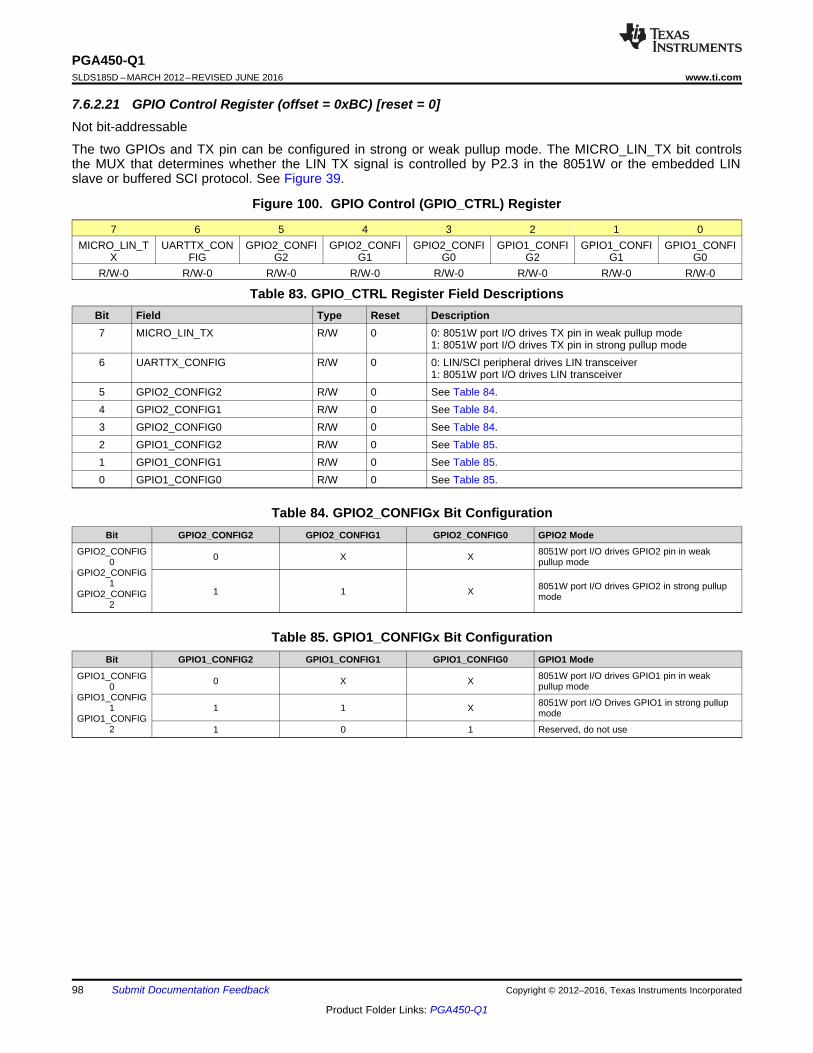
98
PGA450-Q1SLDS185D –MARCH 2012–REVISED JUNE 2016 www.ti.com
Product Folder Links: PGA450-Q1
Submit Documentation Feedback Copyright © 2012–2016, Texas Instruments Incorporated
7.6.2.21 GPIO Control Register (offset = 0xBC) [reset = 0]Not bit-addressable
The two GPIOs and TX pin can be configured in strong or weak pullup mode. The MICRO_LIN_TX bit controlsthe MUX that determines whether the LIN TX signal is controlled by P2.3 in the 8051W or the embedded LINslave or buffered SCI protocol. See Figure 39.
Figure 100. GPIO Control (GPIO_CTRL) Register
7 6 5 4 3 2 1 0MICRO_LIN_T
XUARTTX_CON
FIGGPIO2_CONFI
G2GPIO2_CONFI
G1GPIO2_CONFI
G0GPIO1_CONFI
G2GPIO1_CONFI
G1GPIO1_CONFI
G0R/W-0 R/W-0 R/W-0 R/W-0 R/W-0 R/W-0 R/W-0 R/W-0
Table 83. GPIO_CTRL Register Field DescriptionsBit Field Type Reset Description7 MICRO_LIN_TX R/W 0 0: 8051W port I/O drives TX pin in weak pullup mode
1: 8051W port I/O drives TX pin in strong pullup mode6 UARTTX_CONFIG R/W 0 0: LIN/SCI peripheral drives LIN transceiver
1: 8051W port I/O drives LIN transceiver5 GPIO2_CONFIG2 R/W 0 See Table 84.4 GPIO2_CONFIG1 R/W 0 See Table 84.3 GPIO2_CONFIG0 R/W 0 See Table 84.2 GPIO1_CONFIG2 R/W 0 See Table 85.1 GPIO1_CONFIG1 R/W 0 See Table 85.0 GPIO1_CONFIG0 R/W 0 See Table 85.
Table 84. GPIO2_CONFIGx Bit ConfigurationBit GPIO2_CONFIG2 GPIO2_CONFIG1 GPIO2_CONFIG0 GPIO2 Mode
GPIO2_CONFIG0
GPIO2_CONFIG1
GPIO2_CONFIG2
0 X X 8051W port I/O drives GPIO2 pin in weakpullup mode
1 1 X 8051W port I/O drives GPIO2 in strong pullupmode
Table 85. GPIO1_CONFIGx Bit ConfigurationBit GPIO1_CONFIG2 GPIO1_CONFIG1 GPIO1_CONFIG0 GPIO1 Mode
GPIO1_CONFIG0
GPIO1_CONFIG1
GPIO1_CONFIG2
0 X X 8051W port I/O drives GPIO1 pin in weakpullup mode
1 1 X 8051W port I/O Drives GPIO1 in strong pullupmode
1 0 1 Reserved, do not use

99
PGA450-Q1www.ti.com SLDS185D –MARCH 2012–REVISED JUNE 2016
Product Folder Links: PGA450-Q1
Submit Documentation FeedbackCopyright © 2012–2016, Texas Instruments Incorporated
7.6.2.22 Clock Select Register (offset = 0xBD) [reset = 0]Not bit-addressable
This register controls the MUX that determines the source of the system clock. See the Clock section foradditional information.
Figure 101. Clock Select (CLK_SEL) Register
7 6 5 4 3 2 1 0— CLK_SEL1 CLK_SEL0
R/W-0 R/W-0 R/W-0
Table 86. CLK_SEL Register Field DescriptionsBit Field Type Reset Description7-2 R/W 01 CLK_SEL1 R/W 0 See Table 87.0 CLK_SEL0 R/W 0 See Table 87.
Table 87. CLK_SELx Bit ConfigurationsCLK_SEL1 CLK_SEL0 CLOCK MODE0 0 Internal clock. Ignore synchronization pulse received on the LIN bus0 1 Internal clock. Process synchronization pulse received on the LIN bus1 0 External crystal clock1 1 Internal clock. Ignore synchronization pulse received on the LIN bus.
7.6.2.23 Watchdog Enable Register (offset = 0xBE) [reset = 0]Not bit-addressable
The oscillator watchdog resets the 8051W core if the main oscillator or external crystal oscillator falls outside thevalid range. The software watchdog must be serviced by software every 250ms or it will reset the 8051W core.Both of these watchdogs can be enabled or disabled with this register. See the Main Oscillator Watchdog sectionfor additional information on both of these watchdogs.
Figure 102. Watchdog Enable (WD_EN) Register
7 6 5 4 3 2 1 0— SW_WD_EN OSC_WD_EN
R/W-0 R/W-0 R/W-0
Table 88. WD_EN Register Field DescriptionsBit Field Type Reset Description7-2 R/W 01 SW_WD_EN R/W 0 0: Disable software watchdog.
1: Enable software watchdog.0 OSC_WD_EN R/W 0 0: Disable oscillator watchdog.
1: Enable oscillator watchdog.

100
PGA450-Q1SLDS185D –MARCH 2012–REVISED JUNE 2016 www.ti.com
Product Folder Links: PGA450-Q1
Submit Documentation Feedback Copyright © 2012–2016, Texas Instruments Incorporated
7.6.2.24 LIN/SCI Select Register (offset = 0xBF) [reset = 0]Not bit-addressable
The LIN_SCI bit selects between using the embedded LIN2.1 slave protocol or SCI buffered mode. SCI bufferedmode can transmit or receive 8 bytes of data, beyond that the communication protocol is determined by what isprogrammed in the 8051W software. See the LIN 2.1 Slave and Buffered SCI section for additional information.
Figure 103. LIN/SCI Select (LIN_SCI) Register
7 6 5 4 3 2 1 0— LIN_SCI
R/W-0 R/W-0
Table 89. LIN_SCI Register Field DescriptionsBit Field Type Reset Description7-1 R/W 00 LIN_SCI R/W 0 0: LIN bus operates with LIN protocol.
1: LIN bus operates in SCI mode.
7.6.2.25 EEPROM Control Register (offset = 0xC0) [reset = 0]Bit-addressable
The RELOAD bit in this register copies the contents of the EEPROM into the EEPROM cahce. The WRITE bitprograms the EEPROM with the values stored in the EEPROM cache. Programming starts when the WRITE bitis set to 1. The WRITe bit reamins at 1 until the programming is completed, at which point it drops back to 0. Seethe EEPROM Memory Organization section for additional information.
Figure 104. EEPROM Control (EE_CTRL) Register
7 6 5 4 3 2 1 0— — RELOAD WRITE/EE_ST
ATUSR/W-0 R-0 W-0 R/W-0
Table 90. EE_CTRL Register Field DescriptionsBit Field Type Reset Description7-3 R/W 02 R 01 RELOAD W 0 0: No action
1: Reload EEPROM contents to EEPROM buffer.0 WRITE/EE_STATUS R/W 0 Write:
0: No action1: Program data in EEPROM buffer into EEPROM.Read:0: EEPROM programming is idle.1: EEPROM is being programmed.

101
PGA450-Q1www.ti.com SLDS185D –MARCH 2012–REVISED JUNE 2016
Product Folder Links: PGA450-Q1
Submit Documentation FeedbackCopyright © 2012–2016, Texas Instruments Incorporated
7.6.2.26 Status 1 (STATUS1) Register (offset = 0xC1) [reset = 0]Not bit-addressable
This register stores power-block diagnostic information as well as information about self-tests. For moreinformation see the Diagnostics section and the Internal ASIC TRIM Validity for the trim test and the FIFO RAMtest.
Figure 105. Status 1 (STATUS1) Register
7 6 5 4 3 2 1 0– TRIM_FAIL MBIST_DONE MBIST_FAIL VPWR_OV AVDD_UV AVDD_OC RBIAS_OC
R/W-0 R-0 R-0 R-0 R-0 R-0 R-0 R-0
Table 91. STATUS1 Register Field DescriptionsBit Field Type Reset Description7 R/W 06 TRIM_FAIL R 0 0: Internal ASIC trim values not corrupted
1: Internal ASIC trim values corrupted5 MBIST_DONE R 0 0: FIFO RAM built-in self-test complete
1: FIFO RAM built-in self-test did not complete.4 MBIST_FAIL R 0 0: FIFO RAM built-in self-test passed.
1: FIFO RAM built-in self-test did not pass or did not start.3 VPWR_OV R 0 0: No overvoltage on VPWR pin
1: Overvoltage on VPWR pin2 AVDD_UV R 0 0: No undervoltage on AVDD pin
1: AVDD pin voltage < 4.2 V nominal1 AVDD_OC R 0 0: No overcurrent on AVDD pin
1: AVDD pin current > 55 mA nominal0 RBIAS_OC R 0 0: No overcurrent on RBIAS pin
1: RBIAS pin current > 63 µA nominal

102
PGA450-Q1SLDS185D –MARCH 2012–REVISED JUNE 2016 www.ti.com
Product Folder Links: PGA450-Q1
Submit Documentation Feedback Copyright © 2012–2016, Texas Instruments Incorporated
7.6.2.27 Status 2 Register (offset = 0xC2) [reset = 0]Not bit-addressable
The VREG_RDY bit is set to 1 when the VREG pin is close to the programmed voltage. The VREG pin should beready before starting a burst. After the burst is completed, the SAT_DONE bit indicates when the voltageenvelope at the LIM pin has decreased to below the programmed saturation threshold. The time that this takes isstored in the SAT_TIME register.
The WD_TO_SW and WD_TO_OSC bits indicate the status of the software and oscillator watchdogs. Note thatboth watchdogs must be enabled in the WD_EN register to use.
The LSA_FLT and LSB_FLT bits are diagnostic flags for the low-side FET drivers which protect the FETs fromsinking excessive currents. This diagnostic must be enabled in the LS_FAULT_LOGIC_EN bit in CONTROL_1register before use.
Figure 106. Status 2 (STATUS2) Register
7 6 5 4 3 2 1 0— WD_TO_OSC LSB_FAULT LSA_FAULT WD_TO_SW SAT_DONE VREG_READY
R/W-0 R-0 R-0 R-0 R-0 R-0 R-0
Table 92. STATUS2 Register Field DescriptionsBit Field Type Reset Description7-0 R/W 05 WD_TO_OSC R 0 0: Internal ocillator is normal.
1: Internal oscillator is abrnormal.4 LSB_FAULT R 0 0: No Fault on LSB
1: Fault on LSB3 LSA_FAULT R 0 0: No fault on LSA
1: Fault on LSA2 WD_TO_SW R 0 0: Software watchdog has not timed out.
1: Software watchdog has timed out and the micro has beenreset.
1 SAT_DONE R 0 0: Echo signal is not below saturation threshold.1: Echo signal is below saturation threshold.
0 VREG_READY R 0 0: VREG is not in regulation.1: VREG is less than 200 mV (nominal) below set point selectedby VREG_SEL bits.

103
PGA450-Q1www.ti.com SLDS185D –MARCH 2012–REVISED JUNE 2016
Product Folder Links: PGA450-Q1
Submit Documentation FeedbackCopyright © 2012–2016, Texas Instruments Incorporated
7.6.2.28 Power Mode Register (offset = 0xC3) [reset = 0]Not bit-addressable
The ACTIVE_EN bit enables the support circtuitry related to burst generation and echo processing. This bit mustbe set before enabling burst generation or echo processing (both enabled in the EN_CTRL register).
The VREG_EN bit enables a 100-mA current source to charge an external capacitor. This can then be used todrive the primary of a trasformer. The VREG voltage can be controlled through the VREG_SEL register. See theVREG section for additional information.
Figure 107. Power Mode (PWR_MODE) Register
7 6 5 4 3 2 1 0— VREG_EN ACTIVE_EN
R/W-0 R/W-1 R/W-0
Table 93. PWR_MODE Register Field DescriptionsBit Field Type Reset Description7-2 R/W 01 VREG_EN R/W 0 0: VREG is disabled.
1: VREG is enabled.0 ACTIVE_EN R/W 0 0: EEPROM, VPWR_MON, LNA, LS diagnostics, OUTA, OUTB,
ADC are disabled.1: All the foregoing are enabled.
7.6.2.29 Datapath and SCI Control Register (offset = 0xC4) [reset = 0]Not bit-addressable
This register controls what is loaded into the FIFO RAM. By default, the FIFO is loaded with the digital datapathoutput, but the FIFO_ADC gives the option of bypassing the datapath altogether and loading the FIFO directlyfrom the ADC. The FIFO_PEAKDET bit determines whether or not the low-pass filter is used in the digitaldatapath.
The SCI_TX_EN bit is used while transmitting through SCI. See the SCI Buffered Mode section for additionalinformation on SCI communication procedures.
Figure 108. Datapath and SCI Control (DP_SCI_CTRL) Register
7 6 5 4 3 2 1 0— FIFO_ADC SCI_TX_EN FIFO_PEAKDE
TR/W-0 R/W-0 R/W-1 R/W-1
Table 94. DP_SCI_CTRL Register Field DescriptionsBit Field Type Reset Description7-3 R/W 02 FIFO_ADC R/W 0 0: FIFO is loaded with digital datapath output
1: FIFO is loaded with ADC output.1 SCI_TX_EN R/W 0 0: No action
1: SCI transmit enable0 FIFO_PEAKDET R/W 0 0: In the digital datapath, the lowpass filter is used.
1: In the digital datapath, the lowpass filter is bypassed and thepeak-detector output is used (No low-pass filtering).

104
PGA450-Q1SLDS185D –MARCH 2012–REVISED JUNE 2016 www.ti.com
Product Folder Links: PGA450-Q1
Submit Documentation Feedback Copyright © 2012–2016, Texas Instruments Incorporated
7.6.2.30 FIFO Control Register (offset = 0xC5) [reset = ]Not bit-addressable
The digital datapath has a resolution of 12 bits; however, to conserve space in the FIFO RAM, there are severaloptions about how to store the data from the datapath into the FIFO. All 12 bits can be stored, which effectivelyhalves the number of data points that can be stored in the FIFO. The other three options include the lower eightbits, the upper eight bits, and the middle eight bits. The lower and middle eight bit options also include asaturation check. If there is an overflow, then 0xFF is stored instead of what the lower or middle eight bitsactually was.
If FIFO rollover mode is enabled, then the FIFO write pointer will roll over to 0 after all 768 bytes in the FIFOhave been written to. After the write pointer rolls over, the FIFO RAM will continue to fill with samples from thedigital datapath.
Figure 109. FIFO Control (FIFO_CTRL) Register
7 6 5 4 3 2 1 0— ROLLOVER FMODE1 FMODE0
R/W-0 R/W-0 R/W-1 R/W-1
Table 95. FIFO_CTRL Register Field DescriptionsBit Field Type Reset Description7 R/W 02 ROLLOVER R/W 0 0: FIFO rolls at the end.
1: No rollover of the FIFO1 FMODE1 R/W 0 See Table 96.0 FMODE0 R/W 0 See Table 96.
Table 96. FMODEx Bit ConfigurationFMODE1 FMODE0 DATAPATH BITS STORED INTO THE FIFO
0 0 datapath bits [11:0]0 1 datapath bits [11:4]1 0 datapath bits [7:0] with saturation check on datapath bits [11:8]1 1 datapath bits [10:3] with saturation check on datapath bit [11]

105
PGA450-Q1www.ti.com SLDS185D –MARCH 2012–REVISED JUNE 2016
Product Folder Links: PGA450-Q1
Submit Documentation FeedbackCopyright © 2012–2016, Texas Instruments Incorporated
7.6.2.31 Enable Control Register (offset = 0xC8) [reset = 0]Bit Addressable
The EN_CTRL register is used to initiate a distance measurement. BURST_X_EN enables a burst on the low-side drivers, ECHO_EN starts to fill the FIFO with data from the digital datapath, SAT_EN triggers a saturationmeasurement for diagnostic purposes, and CAP_FR_TMR captures the free running timer to the free runningtimer shadow register. These can all be triggered at the same time or individually depending on the application.
Figure 110. Enable Control (EN_CTRL) Register
7 6 5 4 3 2 1 0CAP_FR_TMR — ECHO_EN SAT_EN BURST_B_EN BURST_A_EN
W-0 R/W-0 R/W-0 R/W-0 W-0 W-0
Table 97. EN_CTRL Register Field DescriptionsBit Field Type Reset Description7 CAP_FR_TMR W 0 0: No action
1: Capture free-running timer value to ESFR FRT.6-4 R/W 03 ECHO_EN R/W 0 0: Disable echo processing – the FIFO is not filled.
1: Enable echo processing – the FIFO starts filling after theblanking timer expires.
2 SAT_EN R/W 0 0: Disable saturation monitor function.1: Enable saturation monitor function.
1 BURST_B_EN W 0 0: No Action1: Enable burst on OUTB in single-ended
0 BURST_A_EN W 0 0: No action1: Enable burst on OUTA in single-ended and OUTA/OUTB inpush-pull.
7.6.2.32 LIN/SCI Rx Data (RX_DATAx) Register (offset = 0xC9 to 0xD1) [reset = 0]Not bit-addressable
Received data from LIN/SCI is stored in the RX_DATAx register. See the LIN 2.1 Slave and Buffered SCI sectionfor more information about LIN/SCI communication.
Figure 111. LIN/SCI Rx Data (RX_DATAx) Register
7 6 5 4 3 2 1 0RX_DATAx[7] RX_DATAx[6] RX_DATAx[5] RX_DATAx[4] RX_DATAx[3] RX_DATAx[2] RX_DATAx[1] RX_DATAx[0]
R-0 R-0 R-0 R-0 R-0 R-0 R-0 R-0
Table 98. RX_DATAx Register Field DescriptionsBit Field Type Reset Description7-0 RX_DATAx[7:0] R 0

106
PGA450-Q1SLDS185D –MARCH 2012–REVISED JUNE 2016 www.ti.com
Product Folder Links: PGA450-Q1
Submit Documentation Feedback Copyright © 2012–2016, Texas Instruments Incorporated
7.6.2.33 LIN PID Register (offset = 0xD2) [reset = 0]Not bit-addressable
The LIN_PID register is used to store the received PID frame from the most recent LIN message. This can beinterpreted by the PGA450-Q1 application firmware to determine how to respond to the message. See the LIN2.1 Slave and Buffered SCI section for more information about LIN/SCI communication.
Figure 112. LIN PID (LIN_PID) Register
7 6 5 4 3 2 1 0PID7 PID6 PID5 PID4 PID3 PID2 PID1 PID0R-0 R-0 R-0 R-0 R-0 R-0 R-0 R-0
Table 99. LIN_PID Register Field DescriptionsBit Field Type Reset Description7 PID7 R 06 PID6 R 05 PID5 R 04 PID4 R 03 PID3 R 02 PID2 R 01 PID1 R 00 PID0 R 0
7.6.2.34 LIN/SCI Tx Data Registers (offset = 0xD3 to 0xDA) [reset = 0]Not bit-addressable
Data to be transmitted over LIN/SCI from the PGA450-Q1 must be programmed to the TX_DATAx registerbefore triggering a transmit message via the RX_TX bit in the LIN_CTRL register. The number of bytestransmitted is set by the DATA_CNT register. See the LIN 2.1 Slave and Buffered SCI section for moreinformation about LIN/SCI communication.
Figure 113. LIN/SCI Tx Data (TX_DATAx) Registers
7 6 5 4 3 2 1 0TX_DATAx[7] TX_DATAx[6] TX_DATAx[5] TX_DATAx[4] TX_DATAx[3] TX_DATAx[2] TX_DATAx[1] TX_DATAx[0]
R/W-0 R/W-0 R/W-0 R/W-0 R/W-0 R/W-0 R/W-0 R/W-0
Table 100. TX_DATAx Register Field DescriptionsBit Field Type Reset Description7-0 TX_DATAx[7:0] R/W 0

107
PGA450-Q1www.ti.com SLDS185D –MARCH 2012–REVISED JUNE 2016
Product Folder Links: PGA450-Q1
Submit Documentation FeedbackCopyright © 2012–2016, Texas Instruments Incorporated
7.6.2.35 LIN/SCI Data Count Register (offset = 0xDB) [reset = 0]Not bit-addressable
The DATA_CNT register determines how many bytes of data will be sent from the TX_DATAx register when aLIN/SCI transmit is initiated. When in SCI mode, the minimum DATA_CNT should be. In both LIN and SCI mode,the maximum value of DATA_CNT should be 8. See the LIN 2.1 Slave and Buffered SCI section for moreinformation about LIN/SCI communication.
Figure 114. LIN/SCI Data Count (DATA_CNT) Register
7 6 5 4 3 2 1 0— CNT3 CNT2 CNT1 CNT0
R/W-0 R/W-0 R/W-0 R/W-0 R/W-0
Table 101. DATA_CNT Register Field DescriptionsBit Field Type Reset Description7-4 R/W 03 CNT3 R/W 02 CNT2 R/W 01 CNT1 R/W 00 CNT0 R/W 0
7.6.2.36 LIN Configuration Register (offset = 0xDC) [reset = 0x40]Not bit-addressable
The LIN_CFG register sets the checksum type used and LIN diagnostics used. See the LIN 2.1 Slave andBuffered SCI section for more information about LIN/SCI communication.
Figure 115. LIN Configuration (LIN_CFG) Register
7 6 5 4 3 2 1 0BIT_TOL CS_METHOD CLR_ERR INTERBYTE_S
PCHOLD — IGNORE_DIAG —
R/W-0 R/W-1 R/W-0 R/W-0 R/W-0 R/W-0 R/W-0 R/W-0
Table 102. LIN_CFG Register Field DescriptionsBit Field Type Reset Description7 BIT_TOL R/W 0 0: Normal bit-time tolerance for the STOP bit transmitted after
PID and data. The nominal is 15% of the expected bit rate.1: Doubles the bit-time tolerance to 30% for the STOP bittransmitted after PID and data.
6 CS_METHOD R/W 1 0: Classic checksum1: Enhanced checksum
5 CLR_ERR R/W 0 0: Do not clear LIN error log register (LIN_STATUS). The clearoccurs only between frames.1: Clear error log register (LIN_STATUS).
4 INTERBYTE_SPC R/W 0 0: 1 bit of inter-byte space during transmission of data bytes byPGA450-Q11: 2 bits of inter-byte space during transmission of data bytes byPGA450-Q1
3 HOLD R/W 0 0: LIN frame is not ignored.1: LIN Frame is ignored; that is, the LIN slave protocol does notprocess the break field.
2 R/W 0 This bit should always be written as 0; the user software shouldnot write a 1 to this bit.
1 IGNORE_DIAG R/W 0 0: Wait for data bytes after PID is received.1: Wait for break field after PID is received.
0 R/W 0 This bit should always be written as 0; the user software shouldnot write a 1 to this bit.

108
PGA450-Q1SLDS185D –MARCH 2012–REVISED JUNE 2016 www.ti.com
Product Folder Links: PGA450-Q1
Submit Documentation Feedback Copyright © 2012–2016, Texas Instruments Incorporated
7.6.2.37 LIN Control Register (offset = 0xDD) [reset = 0]Not bit-addressable
The RX_TX bit initiates a receive or transmit for LIN or SC depending on the mode currently chosen by theLIN_SCI register. See the LIN 2.1 Slave and Buffered SCI section for more information about LIN/SCIcommunication.
Figure 116. LIN Control (LIN_CTRL) Register
7 6 5 4 3 2 1 0— RX_TX
R/W-0 R/W-0
Table 103. LIN_CTRL Register Field DescriptionsBit Field Type Reset Description7-1 R/W 00 RX_TX R/W 0 0: Receive data on LIN bus
1: Transmit data on LIN bus
7.6.2.38 LIN STATUS Register (offset = 0xDE) [reset = 0]Not bit-addressable
The LIN_STATUS register holds the LIN diagnostics, parity, and checksum information. See the LIN 2.1 Slaveand Buffered SCI section for more information about LIN/SCI communication.
Figure 117. LIN STATUS (LIN_STATUS) Register
7 6 5 4 3 2 1 0— BREAK_DEL SYNC_LONG SYNC_SHORT STOP_BIT_SH
ORTSTOP_BIT_VA
LPARITY CHECKSUM
R-0 R-0 R-0 R-0 R-0 R-0 R-0 R-0
Table 104. LIN_STATUS Register Field DescriptionsBit Field Type Reset Description7 R 06 BREAK_DEL R 0 0: Break delimiter normal
1: Break delimiter is shorter than expected.5 SYNC_LONG R 0 0: Sync is not long.
1: Sync is longer than expected (based on fixed time of 50µs/bit)
4 SYNC_SHORT R 0 0: Sync is not short.1: Sync is shorter than expected (based on fixed time of 50µs/bit).
3 STOP_BIT_SHORT R 0 0: Stop bit is normal.1: Stop bit of PID and data is short (based on configuration of bitrate tolerance).
2 STOP_BIT_VAL R 0 0: Stop bit valid1: Stop bit was not set after 8th LIN bit was received ortransmitted
1 PARITY R 0 0: PID parity no error1: PID parity error
0 CHECKSUM R 0 0: Checksum normal1: Checksum error

109
PGA450-Q1www.ti.com SLDS185D –MARCH 2012–REVISED JUNE 2016
Product Folder Links: PGA450-Q1
Submit Documentation FeedbackCopyright © 2012–2016, Texas Instruments Incorporated
7.6.2.39 FIFO Pointer (FIFO_POINTER) RegistersNot bit-addressable
The FIFO pointer registers indicate the current location in the FIFO RAM read to be written to once a sample isavailable from the digital datapath. By checking the current status of the FIFO pointer in the PGA450-Q1application firmware, the user can ensure that the algorithm processing the echo data in the FIFO does notsurpass the valid available data.
7.6.2.39.1 FIFO Pointer MSB Register (offset = 0xDF) [reset = 0]
Figure 118. FIFO Pointer MSB (FIFO_POINTER_MSB) Register
7 6 5 4 3 2 1 0— FIFO_PTR[9] FIFO_PTR[8]
R-0 R-0 R-0
Table 105. FIFO_POINTER_MSB Register Field DescriptionsBit Field Type Reset Description7-2 R 01-0 FIFO_PTR[9:8] R 0

110
PGA450-Q1SLDS185D –MARCH 2012–REVISED JUNE 2016 www.ti.com
Product Folder Links: PGA450-Q1
Submit Documentation Feedback Copyright © 2012–2016, Texas Instruments Incorporated
7.6.2.39.2 FIFO Pointer LSB Register (offset = 0xE1) [reset = 0]
Figure 119. FIFO Pointer LSB (FIFO_POINTER_LSB) Register
7 6 5 4 3 2 1 0FIFO_PTR[7] FIFO_PTR[6] FIFO_PTR[5] FIFO_PTR[4] FIFO_PTR[3] FIFO_PTR[2] FIFO_PTR[1] FIFO_PTR[0]
R-0 R-0 R-0 R-0 R-0 R-0 R-0 R-0
Table 106. FIFO_POINTER_LSB Register Field DescriptionsBit Field Type Reset Description7-0 FIFO_PTR[7:0] R 0
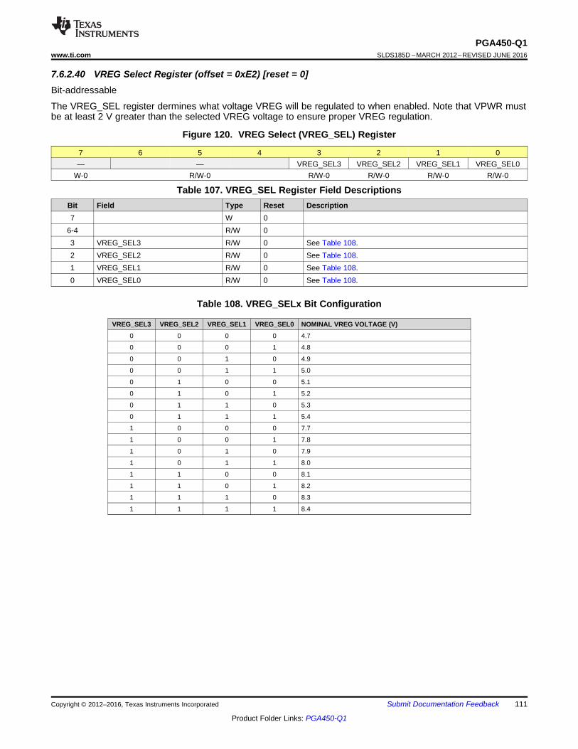
111
PGA450-Q1www.ti.com SLDS185D –MARCH 2012–REVISED JUNE 2016
Product Folder Links: PGA450-Q1
Submit Documentation FeedbackCopyright © 2012–2016, Texas Instruments Incorporated
7.6.2.40 VREG Select Register (offset = 0xE2) [reset = 0]Bit-addressable
The VREG_SEL register dermines what voltage VREG will be regulated to when enabled. Note that VPWR mustbe at least 2 V greater than the selected VREG voltage to ensure proper VREG regulation.
Figure 120. VREG Select (VREG_SEL) Register
7 6 5 4 3 2 1 0— — VREG_SEL3 VREG_SEL2 VREG_SEL1 VREG_SEL0
W-0 R/W-0 R/W-0 R/W-0 R/W-0 R/W-0
Table 107. VREG_SEL Register Field DescriptionsBit Field Type Reset Description7 W 0
6-4 R/W 03 VREG_SEL3 R/W 0 See Table 108.2 VREG_SEL2 R/W 0 See Table 108.1 VREG_SEL1 R/W 0 See Table 108.0 VREG_SEL0 R/W 0 See Table 108.
Table 108. VREG_SELx Bit Configuration
VREG_SEL3 VREG_SEL2 VREG_SEL1 VREG_SEL0 NOMINAL VREG VOLTAGE (V)
0 0 0 0 4.7
0 0 0 1 4.8
0 0 1 0 4.9
0 0 1 1 5.0
0 1 0 0 5.1
0 1 0 1 5.2
0 1 1 0 5.3
0 1 1 1 5.4
1 0 0 0 7.7
1 0 0 1 7.8
1 0 1 0 7.9
1 0 1 1 8.0
1 1 0 0 8.1
1 1 0 1 8.2
1 1 1 0 8.3
1 1 1 1 8.4

112
PGA450-Q1SLDS185D –MARCH 2012–REVISED JUNE 2016 www.ti.com
Product Folder Links: PGA450-Q1
Submit Documentation Feedback Copyright © 2012–2016, Texas Instruments Incorporated
7.6.2.41 Sync Count (SYNC_COUNT) RegistersNot bit-addressable
The SYNC_COUNT register can be used to determine the success of a LIN sync operation. This register storesthe measured width of the LIN sync field. See the Clock Synchronizer Using the SYNC Field in the LIN Bussection for more details.
7.6.2.41.1 Sync Count MSB Register (offset = 0xE3) [reset = 0]
Figure 121. Sync Count MSB (SYNC_COUNT_MSB) Register
7 6 5 4 3 2 1 0SC[15] SC[14] SC[13] SC[12] SC[11] SC[10] SC[9] SC[8]
R-0 R-0 R-0 R-0 R-0 R-0 R-0 R-0
Table 109. SYNC_COUNT_MSB Register Field DescriptionsBit Field Type Reset Description7-0 SC[15:8] R 0
7.6.2.41.2 Sync Count LSB Register (offset = 0xE4) [reset = 0]
Figure 122. Sync Count LSB (SYNC_COUNT_LSB) Register
7 6 5 4 3 2 1 0SC[7] SC[6] SC[5] SC[4] SC[3] SC[2] SC[1] SC[0]R-0 R-0 R-0 R-0 R-0 R-0 R-0 R-0
Table 110. SYNC_COUNT_LSB Register Field DescriptionsBit Field Type Reset Description7-0 SC[7:0] R 0

113
PGA450-Q1www.ti.com SLDS185D –MARCH 2012–REVISED JUNE 2016
Product Folder Links: PGA450-Q1
Submit Documentation FeedbackCopyright © 2012–2016, Texas Instruments Incorporated
7.6.2.42 TEMP/DAC Control Register (offset = 0xE5) [reset = 0]Bit-addressable
Figure 123. TEMP/DAC Control (TEMP_DAC_CTRL) Register
7 6 5 4 3 2 1 0— — TS_DAC_MOD
ETS_DAC_EN
W-0 R/W-0 W-0 W-0
Table 111. TEMP_DAC_CTRL Register Field DescriptionsBit Field Type Reset Description7 W 0
6-2 R/W 01 TS_DAC_MODE W 0 0: Temperature sensor
1: Digital datapath0 TS_DAC_EN W 0 0: Temperature sensor DAC powered off
1: Temperature sensor DAC powered on
7.6.2.43 Oscillator Sync Control Register (offset = 0xE6) [reset = 0]Bit-addressable
The OSx bits determine how much of an oscillator frequency shift is implemented. This can be determined fromthe LIN synchronization algorithm or directly from the 8051W application code. See Table 3 for details on whatfrequency shifts are implemented from the OSx bits.
Figure 124. Oscillator Sync Control (OSC_SYNC_CTRL) Register
7 6 5 4 3 2 1 0— OVR OS5 OS4 OS3 OS2 OS1 OS0
W-0 R/W-0 R/W-0 R/W-0 R/W-0 R/W-0 W-0 W-0
Table 112. OSC_SYNC_CTRL Register Field DescriptionsBit Field Type Reset Description7 W 06 OVR R/W 0 0: OS[5:0] are read-only for 8051W, clock synchronization
algorithm updates OS[5:0] bits.1: 8051W updates OS[5:0] bits, clock synchronization algorithmdoes not update OS[5:0] bits.
5 OS5 R/W 04 OS4 R/W 03 OS3 R/W 02 OS2 R/W 01 OS1 W 00 OS0 W 0

114
PGA450-Q1SLDS185D –MARCH 2012–REVISED JUNE 2016 www.ti.com
Product Folder Links: PGA450-Q1
Submit Documentation Feedback Copyright © 2012–2016, Texas Instruments Incorporated
7.6.3 TEST Registers
7.6.3.1 ANALOG Test MUX Register (offset = 0xE9) [reset = 0]Not bit-addressable
The AMUX register determines what the output of the DACO pin is. Both options for the DAC output are intendedfor development purposes as they provide ways to view the echo signal on an oscilloscope before and after thedigital datapath.
Figure 125. ANALOG Test MUX (AMUX) Register
7 6 5 4 3 2 1 0— AMUX3 AMUX2 AMUX1 AMUX0
R/W-0 R/W-0 R/W-0 R/W-0 R/W-0
Table 113. AMUX Register Field DescriptionsBit Field Type Reset Description7-4 R/W 03 AMUX3 R/W 0 See Table 114.2 AMUX2 R/W 0 See Table 114.1 AMUX1 R/W 0 See Table 114.0 AMUX0 R/W 0 See Table 114.
Table 114. AMUX3:0 Bit ConfigurationAMUX3:AMUX0 (Hexadecimal) Output on TESTO_A Description
01 DAC OUTPUT Digital datapath output voltage04 LNA OUTPUT Low-noise amplifier output

115
PGA450-Q1www.ti.com SLDS185D –MARCH 2012–REVISED JUNE 2016
Product Folder Links: PGA450-Q1
Submit Documentation FeedbackCopyright © 2012–2016, Texas Instruments Incorporated
7.6.3.2 DIGITAL Test MUX Register (offset = 0xEA) [reset = 0]Not bit-addressable
Figure 126. DIGITAL Test MUX (DMUX) Register
7 6 5 4 3 2 1 0— DMUX4 DMUX3 DMUX2 DMUX1 DMUX0
R/W-0 R/W-0 R/W-0 R/W-0 R/W-0 R/W-0
Table 115. DMUX Register Field DescriptionsBit Field Type Reset Description7-5 R/W 04 DMUX4 R/W 0 See Table 116.3 DMUX3 R/W 0 See Table 116.2 DMUX2 R/W 0 See Table 116.1 DMUX1 R/W 0 See Table 116.0 DMUX0 R/W 0 See Table 116.
Table 116. DMUX4:0 Bit ConfigurationDMUX4:DMUX0(Hexadecimal)
Output onTESTO_D Description Output on GPIO1 Description Output on GPIO2 Description
01 SAT_EN Saturation enable SAT_DONE Saturation Done SAT_MONSaturation
ComparatorOutput
04 LIN_RXD LIN receive LIN_TXD LIN Transmit
08 FIFO_UPDATE
Pulse isgenerated whenFIFO pointer is
updated.0A CLK System clock INT_CLK Internal Clock EXT_CLK External Clock

116
PGA450-Q1SLDS185D –MARCH 2012–REVISED JUNE 2016 www.ti.com
Product Folder Links: PGA450-Q1
Submit Documentation Feedback Copyright © 2012–2016, Texas Instruments Incorporated
8 Application and Implementation
NOTEInformation in the following applications sections is not part of the TI componentspecification, and TI does not warrant its accuracy or completeness. TI’s customers areresponsible for determining suitability of components for their purposes. Customers shouldvalidate and test their design implementation to confirm system functionality.
8.1 Application InformationThe PGA450-Q1 must be paired with an external transducer. The PGA450-Q1 drives the transducer and thenfilters and processes the returned echo signal sensed by the transducer. The transducer should be chosenbased on the resonant frequency, input voltage requirements, sensitivity, beam pattern, and decay time. ThePGA450-Q1 meets most transducer requirements by adjusting the driving frequency, driving voltage, andbandpass center frequency. The external transformer should be chosen to meet the input voltage requirementsof the transducer and to have a high-enough saturation current.
The interface options include LIN, SCI, UART, and SPI. The SPI must be used when programming the memoryof the PGA450-Q1, but after that any of the other interfaces can be used for communication. After a distancemeasurement is initiated, the PGA450-Q1 can return the measured distance through a communication interface.
8.2 Typical ApplicationIn the typical application, the PGA450-Q1 is paired with one transducer which are located on one PCB as onesense node. Each PCB uses a three-wire interface, power, ground, and LIN. Multiple PCBs can be connected inparallel as shown in Figure 127. If a different communication method is used, then more wires may be needed.

.
.
.
ECU
LINTransceiver
VBAT
Data Bus
GND VPWR
GND
GND
OUTA
GND
CS
SCLK
Drive_A
LNA
8-bit Core
Digital Datapath
VREG
Oscillator
SDI
SDO
OTP
LIN
EEPROM
PCB
IN
OUTB
Drive_B
AVDD
DVDD
VREGVSUPPLY
X1
X2
VREF
LIM
RBIAS
Data Bus
GND VPWR
OUTA
GND
Drive_A
LNA
VREG
Oscillator
LIN
PGA450-Q1
PCB
IN
OUTB
Drive_B
AVDD
DVDD
VREGVSUPPLY
VREF
LIM
RBIAS
CIN
LIN
LIN
PGA450-Q1
ADC
ADC
GND
GND
CS
SCLK
8-bit Core
Digital Datapath
SDI
SDO
OTP
EEPROM
X1
X2
CIN
117
PGA450-Q1www.ti.com SLDS185D –MARCH 2012–REVISED JUNE 2016
Product Folder Links: PGA450-Q1
Submit Documentation FeedbackCopyright © 2012–2016, Texas Instruments Incorporated
Typical Application (continued)
Figure 127. Typical Application Schematic

T TTUNE PT
SEC
C LC C
L
u �
LSEC
RT
CTUNE CPT
LT
CT
Transducer
118
PGA450-Q1SLDS185D –MARCH 2012–REVISED JUNE 2016 www.ti.com
Product Folder Links: PGA450-Q1
Submit Documentation Feedback Copyright © 2012–2016, Texas Instruments Incorporated
Typical Application (continued)8.2.1 Design ParametersFor this design example, use the following parameters:• ftransducer = 58 kHz• VPWR = 12 V• dmin = 15 cm• dmax = 5 m
8.2.2 Detailed Design Procedure
8.2.2.1 HardwareThe hardware design for the PGA450 consists of selecting a transducer and supporting passive components.When a transducer is selected, the next step in the design process is to select a transformer based on thecharacteristics of the transducer. Figure 128 shows the electrical model of the transducer. The secondarywinding of the transformer should be selected to match the resonant frequency of the transducer. A tuningcapacitor can be used to assist with this requirement.
Figure 128. Transducer and Transformer Electrical Model
(11)
The low-side drivers force a voltage across the transducers equal to the VREG voltage. Either low-side drivercan be used with a single-ended transformer or a center-tapped transformer can be used with both low-sidedrivers for push-pull mode. Single-ended mode causes the voltage on the secondary side of the windings to beapproximately the turn ratio multiplied by the VREG voltage. Push-pull mode doubles the voltage. Select thetransformer, the value of VREG, and circuit configuration based on the VPP value of the transducer. Also considerthat as current is pulled from the VREG capacitor, the voltage at the VREG pin will droop. Finally, ensure that thetransformer saturation current is sufficient.
8.2.2.2 FirmwareThe PGA450-Q1 must be programmed to work with the selected transducer and can be optimized for the desiredrange. For this example, two different firmware settings will be used: one to optimize short-distance detection andone to optimize long-distance detection. Program the registers listed in Table 117 to program the device to workwith the selected transducer.

max sMIN
sound
2 d fDOWNSAMPLE
FIFO V
u u
u
119
PGA450-Q1www.ti.com SLDS185D –MARCH 2012–REVISED JUNE 2016
Product Folder Links: PGA450-Q1
Submit Documentation FeedbackCopyright © 2012–2016, Texas Instruments Incorporated
Typical Application (continued)Table 117. Registers to Tune for Optimization
SHORT DISTANCE OPTIMIZATION LONG DISTANCE OPTIMIZATION
Bandpass filter
BPF_B1_MSB = 0x03BPF_B1_LSB = 0x2DBPF_A2_MSB = 0xECBPF_A2_LSB = 0x3DBPF_A3_MSB = 0xF9BPF_A3_LSB = 0xA5
Downsample rate DOWNSAMPLE = 0x28Low-pass filter LPF_B1_MSB = 0x2D
LPF_B1_LSB = 0x68LPF_A2_MSB = 0x25LPF_A2_LSB = 0x30
Low-side drivers BURST_ONA_MSB = 0x00BURST_ONA_LSB = 0x8A
BURST_OFFA_MSB = 0x00BURST_OFFA_LSB = 0x8ABURST_ONB_MSB = 0x00BURST_ONB_LSB = 0x8A
BURST_OFFB_MSB = 0x00BURST_OFFB_LSB = 0x8A
Pulse count PULSE_CNTA = 0x01 PULSE_CNTA = 0x12Blanking timer BLANKING_TIMER = 0x27 BLANKING_TIMER = 0xFFFIFO mode FIFO_CTRL = 0x07 FIFO_CTRL = 0x06
8.2.2.2.1 Band-pass Filter Coefficients
The bandpass filter coefficients are selected by referring to Table 6 and Table 7. A bandwidth of 4 kHz wasselected for this example. A wider bandwidth can be used if the transducer center frequency has more variationor for applications that must pick up possible frequency shifts caused by movement or environmental conditions.A wider bandwidth corresponds to more noise, therefore, the smallest bandwidth that fits the application shouldbe selected.• BPF_B1_MSB = 0x03• BPF_B1_LSB = 0x2D• BPF_A2_MSB = 0xEC• BPF_A2_LSB = 0x3D• BPF_A3_MSB = 0xF9• BPF_A3_LSB = 0xA5
8.2.2.2.2 Downsample Rate
With only 768 bytes available in the FIFO RAM, the downsample rate allows some flexibility for selecting howoften samples are stored. A smaller downsample rate provides more resolution but the maximum distance storedwill be shorter.
where• dmax = maximum distance detection required of application.• fs = ADC sampling frequency, 1 MHz.• FIFO = FIFO RAM memory size, 768.• vsound = speed of sound, through air at room temp = 343 m/s. (12)
OSC
transducer
FOUT _ A _ON OUT _ A _OFF OUT _B_ON OUT _B_OFF 0x8A
2 f
u
MIN2 5 m 1MHz
DOWNSAMPLE 38768 343 m / su u
u
120
PGA450-Q1SLDS185D –MARCH 2012–REVISED JUNE 2016 www.ti.com
Product Folder Links: PGA450-Q1
Submit Documentation Feedback Copyright © 2012–2016, Texas Instruments Incorporated
(13)
To add some margin, a downsampling rate of 40 was selected for this example, which is 0x28 in hexadecimal.
DOWNSAMPLE = 0x28
8.2.2.2.3 Low-Pass Filter Coefficients
The low-pass filter coefficients are selected by referring to Table 8. For this example, a cutoff frequency of 4 kHzis used. A smaller cutoff frequency can be used to further zoom in around the center frequency of the transducer;however, ensure to consider the transducer frequency variation across process and temperature.• LPF_B1_MSB = 0x2D• LPF_B1_LSB = 0x68• LPF_A2_MSB = 0x25• LPF_A2_LSB = 0x30
8.2.2.2.4 Pulse Count
Th pulse count sets the number of pulses driven by the low-side drivers per measurement burst. To optimize theminimum measurable distance, a small number of pulses should be used. To detect distances farther away,more pulses should be sent to maximize the sent signal strength.• Short distance mode, 1 pulse:
– PULSE_CNTA = 0x01• Long distance mode, 16 pulses:
– PULSE_CNTA = 0x12
8.2.2.2.5 Blanking Timer
The blanking timer setting allows the user to delay when the FIFO RAM begins storing samples. Immediatelyafter the transducer is excited, the signal is too large to extract useful information from. To maximize theefficiency of the data stored in the FIFO, the blanking timer can be used so that this initial saturated section ofdata is not stored. For this example, the blanking time was selected by first examining the resulting waveformwhen the blanking time was 0. From this, the saturated region can be observed. Set the blanking timer to removemost of this saturated region.• Short distance mode, set to remove the saturated echo region from the echo data:
– BLANKING_TIMER = 0x27• Long distance mode, maximize blanking timer to increase maximum distance:
– BLANKING_TIMER = 0xFF
8.2.2.2.6 FIFO Mode
The digital datapath of the PGA450-Q1 is 12 bits; however, storing all 12 bits quickly uses up more of the 768bytes of FIFO RAM which reduces the range of distances that can be measured. An alternative is to store only 8bits in the FIFO RAM. Storing the lower 8 bits maximizes the resolution and is helpful for measuring longdistances. For measuring short distances, minimizing the saturation time is important, therefore, the middle 8 bitscan be used.• Short distance mode, middle 8 bits are stored [10:3]
– FIFO_CTRL = 0x07• Long distance mode, lower 8 bits are stored:
– FIFO_CTRL = 0x06
8.2.2.3 OUT_A and OUT_B On and Off TimesThese on and off times dictate the driving frequency of the low-side drivers. Typically these times will match thecenter frequency of the transducer.
(14)

Distance (m)
Am
plitu
de (
m)
0 200 400 600 800 10000
50
100
150
200
250
300
D002
1 m2 m3 m4 m5 m6 mThreshold in EEPROM
Distance (m)A
mpl
itude
(cm
)0 0.2 0.4 0.6 0.8 1
0
50
100
150
200
250
300
D001
20 cm30 cm50 cmThreshold in EEPROM
121
PGA450-Q1www.ti.com SLDS185D –MARCH 2012–REVISED JUNE 2016
Product Folder Links: PGA450-Q1
Submit Documentation FeedbackCopyright © 2012–2016, Texas Instruments Incorporated
8.2.3 Application CurvesThese application curves show the results of using the settings derived above to measure a 1-m tall, 76-mm widePVC pipe at various distances. Several runs are plotted on top of each other. The y-axis shows the signalstrength of the returned signal and the x-axis shows the distance. To determine where the object is located, athreshold can be used to compare the amplitude of the echo data at each FIFO memory location. When theincoming data surpasses the threshold, the PGA450-Q1 can flag that location as the measured distance. Thisthreshold scheme must be programmed into the microcontroller of the PGA450-Q1.
Figure 129. Long Distance Measurements Figure 130. Short Distance Measurements
9 Power Supply RecommendationsThe PGA450-Q1 can operate from a 7- to 18-V power supply. The device can be connected directly to a batterythrough a reverse battery-protection diode. The ramp-down rate of the power supply must be faster than 1V/msso that the AVDD UV flag remains valid. Read SLDA028 for a full description of this requirement.
The VREG pin can be programmed to regulate from 4.7 to 8.4 V. The VPWR supply voltage must be 2-V greaterthan the VREG voltage to ensure proper regulation.
10 Layout
10.1 Layout GuidelinesThe grounding scheme of the PGA450-Q1 must be planned to reduce noise interference. In particular, thetransducer and supporting circuitry should each have a ground plane connected to the main ground at one point.The LIN line should have a separate ground as well which should also be connected to the main ground at onepoint. This separate ground for LIN is only necessary if a capacitor from the LIN pin to ground is put on thePGA450 PCB. The third grounding network should include everything else, including the power ground.
The PCB trace should go from the LIN pin to the PCB connector in as direct a route as possible to reduce anypossible noise interference. The most noise-sensitive portion of the application circuit is from the transducer tothe IN and LIM pins. This layout should be as direct as possible and should avoid crossing any noisy signalpaths.

VPWR
VREG
LIN
GND
DVDD
XIN
XOUT
GPIO1
GPIO2
RxD
TxD
CIN
IN
LIM
AVDD
VPROG_OTP
VREF
OUTA
GND
OUTB
SDO
SDI
SCLK
CS
GND
RBIAS
DAC0
GND
3 Pin Connector
Sensor Ground
Power Ground
Connect power ground to sensor ground at
one point
Connect OUTA and OUTB to two primary pins of
transformer through vias
Via
Copper trace and pour
Copper trace and pour on bottom layerComponent on bottom layer
VIN LIN GND
Transformer on bottom layer
Transducer
122
PGA450-Q1SLDS185D –MARCH 2012–REVISED JUNE 2016 www.ti.com
Product Folder Links: PGA450-Q1
Submit Documentation Feedback Copyright © 2012–2016, Texas Instruments Incorporated
10.2 Layout Example
Figure 131. PGA450-Q1 Layout Example

123
PGA450-Q1www.ti.com SLDS185D –MARCH 2012–REVISED JUNE 2016
Product Folder Links: PGA450-Q1
Submit Documentation FeedbackCopyright © 2012–2016, Texas Instruments Incorporated
11 Device and Documentation Support
11.1 Documentation Support
11.1.1 Related DocumentationFor related documentation see the following:• Automatic Slave Node Position Detection (SNPD), SLDA038• LIN Demonstration Using PGA450Q1EVM Firmware Rev 2.1, SLDA035• Optimizing Performance of the PGA450-Q1, SLDA037• PGA450-Q1 EVM User’s Guide, SLDU007• PGA450Q1EVM-S User's Guide and TIDA-00151 UART Demo Instructional, SLDU019• PGA450-Q1 Reset Issue During VPWR Ramp Down, SLDA028
11.2 Community ResourceThe following links connect to TI community resources. Linked contents are provided "AS IS" by the respectivecontributors. They do not constitute TI specifications and do not necessarily reflect TI's views; see TI's Terms ofUse.
TI E2E™ Online Community TI's Engineer-to-Engineer (E2E) Community. Created to foster collaborationamong engineers. At e2e.ti.com, you can ask questions, share knowledge, explore ideas and helpsolve problems with fellow engineers.
Design Support TI's Design Support Quickly find helpful E2E forums along with design support tools andcontact information for technical support.
11.3 TrademarksE2E is a trademark of Texas Instruments.All other trademarks are the property of their respective owners.
11.4 Electrostatic Discharge CautionThese devices have limited built-in ESD protection. The leads should be shorted together or the device placed in conductive foamduring storage or handling to prevent electrostatic damage to the MOS gates.
11.5 GlossarySLYZ022 — TI Glossary.
This glossary lists and explains terms, acronyms, and definitions.
12 Mechanical, Packaging, and Orderable InformationThe following pages include mechanical, packaging, and orderable information. This information is the mostcurrent data available for the designated devices. This data is subject to change without notice and revision ofthis document. For browser-based versions of this data sheet, refer to the left-hand navigation.

PACKAGE OPTION ADDENDUM
www.ti.com 9-May-2016
Addendum-Page 1
PACKAGING INFORMATION
Orderable Device Status(1)
Package Type PackageDrawing
Pins PackageQty
Eco Plan(2)
Lead/Ball Finish(6)
MSL Peak Temp(3)
Op Temp (°C) Device Marking(4/5)
Samples
PGA450TPWRQ1 ACTIVE TSSOP PW 28 2000 Green (RoHS& no Sb/Br)
CU NIPDAU Level-2-260C-1 YEAR -40 to 125 PGA450
(1) The marketing status values are defined as follows:ACTIVE: Product device recommended for new designs.LIFEBUY: TI has announced that the device will be discontinued, and a lifetime-buy period is in effect.NRND: Not recommended for new designs. Device is in production to support existing customers, but TI does not recommend using this part in a new design.PREVIEW: Device has been announced but is not in production. Samples may or may not be available.OBSOLETE: TI has discontinued the production of the device.
(2) Eco Plan - The planned eco-friendly classification: Pb-Free (RoHS), Pb-Free (RoHS Exempt), or Green (RoHS & no Sb/Br) - please check http://www.ti.com/productcontent for the latest availabilityinformation and additional product content details.TBD: The Pb-Free/Green conversion plan has not been defined.Pb-Free (RoHS): TI's terms "Lead-Free" or "Pb-Free" mean semiconductor products that are compatible with the current RoHS requirements for all 6 substances, including the requirement thatlead not exceed 0.1% by weight in homogeneous materials. Where designed to be soldered at high temperatures, TI Pb-Free products are suitable for use in specified lead-free processes.Pb-Free (RoHS Exempt): This component has a RoHS exemption for either 1) lead-based flip-chip solder bumps used between the die and package, or 2) lead-based die adhesive used betweenthe die and leadframe. The component is otherwise considered Pb-Free (RoHS compatible) as defined above.Green (RoHS & no Sb/Br): TI defines "Green" to mean Pb-Free (RoHS compatible), and free of Bromine (Br) and Antimony (Sb) based flame retardants (Br or Sb do not exceed 0.1% by weightin homogeneous material)
(3) MSL, Peak Temp. - The Moisture Sensitivity Level rating according to the JEDEC industry standard classifications, and peak solder temperature.
(4) There may be additional marking, which relates to the logo, the lot trace code information, or the environmental category on the device.
(5) Multiple Device Markings will be inside parentheses. Only one Device Marking contained in parentheses and separated by a "~" will appear on a device. If a line is indented then it is a continuationof the previous line and the two combined represent the entire Device Marking for that device.
(6) Lead/Ball Finish - Orderable Devices may have multiple material finish options. Finish options are separated by a vertical ruled line. Lead/Ball Finish values may wrap to two lines if the finishvalue exceeds the maximum column width.
Important Information and Disclaimer:The information provided on this page represents TI's knowledge and belief as of the date that it is provided. TI bases its knowledge and belief on informationprovided by third parties, and makes no representation or warranty as to the accuracy of such information. Efforts are underway to better integrate information from third parties. TI has taken andcontinues to take reasonable steps to provide representative and accurate information but may not have conducted destructive testing or chemical analysis on incoming materials and chemicals.TI and TI suppliers consider certain information to be proprietary, and thus CAS numbers and other limited information may not be available for release.
In no event shall TI's liability arising out of such information exceed the total purchase price of the TI part(s) at issue in this document sold by TI to Customer on an annual basis.

PACKAGE OPTION ADDENDUM
www.ti.com 9-May-2016
Addendum-Page 2


IMPORTANT NOTICE
Texas Instruments Incorporated and its subsidiaries (TI) reserve the right to make corrections, enhancements, improvements and otherchanges to its semiconductor products and services per JESD46, latest issue, and to discontinue any product or service per JESD48, latestissue. Buyers should obtain the latest relevant information before placing orders and should verify that such information is current andcomplete. All semiconductor products (also referred to herein as “components”) are sold subject to TI’s terms and conditions of salesupplied at the time of order acknowledgment.TI warrants performance of its components to the specifications applicable at the time of sale, in accordance with the warranty in TI’s termsand conditions of sale of semiconductor products. Testing and other quality control techniques are used to the extent TI deems necessaryto support this warranty. Except where mandated by applicable law, testing of all parameters of each component is not necessarilyperformed.TI assumes no liability for applications assistance or the design of Buyers’ products. Buyers are responsible for their products andapplications using TI components. To minimize the risks associated with Buyers’ products and applications, Buyers should provideadequate design and operating safeguards.TI does not warrant or represent that any license, either express or implied, is granted under any patent right, copyright, mask work right, orother intellectual property right relating to any combination, machine, or process in which TI components or services are used. Informationpublished by TI regarding third-party products or services does not constitute a license to use such products or services or a warranty orendorsement thereof. Use of such information may require a license from a third party under the patents or other intellectual property of thethird party, or a license from TI under the patents or other intellectual property of TI.Reproduction of significant portions of TI information in TI data books or data sheets is permissible only if reproduction is without alterationand is accompanied by all associated warranties, conditions, limitations, and notices. TI is not responsible or liable for such altereddocumentation. Information of third parties may be subject to additional restrictions.Resale of TI components or services with statements different from or beyond the parameters stated by TI for that component or servicevoids all express and any implied warranties for the associated TI component or service and is an unfair and deceptive business practice.TI is not responsible or liable for any such statements.Buyer acknowledges and agrees that it is solely responsible for compliance with all legal, regulatory and safety-related requirementsconcerning its products, and any use of TI components in its applications, notwithstanding any applications-related information or supportthat may be provided by TI. Buyer represents and agrees that it has all the necessary expertise to create and implement safeguards whichanticipate dangerous consequences of failures, monitor failures and their consequences, lessen the likelihood of failures that might causeharm and take appropriate remedial actions. Buyer will fully indemnify TI and its representatives against any damages arising out of the useof any TI components in safety-critical applications.In some cases, TI components may be promoted specifically to facilitate safety-related applications. With such components, TI’s goal is tohelp enable customers to design and create their own end-product solutions that meet applicable functional safety standards andrequirements. Nonetheless, such components are subject to these terms.No TI components are authorized for use in FDA Class III (or similar life-critical medical equipment) unless authorized officers of the partieshave executed a special agreement specifically governing such use.Only those TI components which TI has specifically designated as military grade or “enhanced plastic” are designed and intended for use inmilitary/aerospace applications or environments. Buyer acknowledges and agrees that any military or aerospace use of TI componentswhich have not been so designated is solely at the Buyer's risk, and that Buyer is solely responsible for compliance with all legal andregulatory requirements in connection with such use.TI has specifically designated certain components as meeting ISO/TS16949 requirements, mainly for automotive use. In any case of use ofnon-designated products, TI will not be responsible for any failure to meet ISO/TS16949.
Products ApplicationsAudio www.ti.com/audio Automotive and Transportation www.ti.com/automotiveAmplifiers amplifier.ti.com Communications and Telecom www.ti.com/communicationsData Converters dataconverter.ti.com Computers and Peripherals www.ti.com/computersDLP® Products www.dlp.com Consumer Electronics www.ti.com/consumer-appsDSP dsp.ti.com Energy and Lighting www.ti.com/energyClocks and Timers www.ti.com/clocks Industrial www.ti.com/industrialInterface interface.ti.com Medical www.ti.com/medicalLogic logic.ti.com Security www.ti.com/securityPower Mgmt power.ti.com Space, Avionics and Defense www.ti.com/space-avionics-defenseMicrocontrollers microcontroller.ti.com Video and Imaging www.ti.com/videoRFID www.ti-rfid.comOMAP Applications Processors www.ti.com/omap TI E2E Community e2e.ti.comWireless Connectivity www.ti.com/wirelessconnectivity
Mailing Address: Texas Instruments, Post Office Box 655303, Dallas, Texas 75265Copyright © 2016, Texas Instruments Incorporated