dac128s085 12-bit micro-power octal digital-to-analog ... · outa outb outc outd oute outf outg...
TRANSCRIPT

OUTA
OUTB
OUTC
OUTD
OUTE
OUTF
OUTG
OUTH
GND
4-wire SPIMCU
(Master)
CO
NT
RO
LLER
VREF1VREF2VDD
2 Individual
References
independent of
VDD
Digital I/O
tolerant of
Master to DAC
rail potential
mismatch
Wide supply range
Product
Folder
Sample &Buy
Technical
Documents
Tools &
Software
Support &Community
DAC128S085SNAS407H –AUGUST 2007–REVISED APRIL 2015
DAC128S085 12-Bit Micro-Power OCTAL Digital-to-Analog Converter With Rail-to-RailOutputs
1 Features 3 DescriptionThe DAC128S085 is a full-featured, general-purpose
1• Ensured MonotonicityOCTAL 12-bit voltage-output digital-to-analog• Low Power Operation converter (DAC) that can operate from a single 2.7-V
• Rail-to-Rail Voltage Output to 5.5-V supply and consumes 1.95 mW at 3 V and4.85 mW at 5 V. The DAC128S085 is packaged in a• Daisy-Chain Capability16-lead WQFN package and a 16-lead TSSOP• Power-on Reset to 0 V package. The WQFN package makes the
• Simultaneous Output Updating DAC128S085 the smallest OCTAL DAC in its class.The on-chip output amplifiers allow rail-to-rail output• Individual Channel Power-Down Capabilityswing, and the 3-wire serial interface operates at• Wide Power Supply Range (2.7 V to 5.5 V)clock rates up to 40 MHz over the entire supply• Dual Reference Voltages With Range of 0.5 V to voltage range. Competitive devices are limited to 25-
VA MHz clock rates at supply voltages in the 2.7-V to• Operating Temperature Range of −40°C to 125°C 3.6-V range. The serial interface is compatible with
standard SPI™, QSPI, MICROWIRE, and DSP• Smallest Package in the Industryinterfaces. The DAC128S085 also offers daisy-chain• Resolution 12 Bits operation, where an unlimited number of
• INL ±8 LSB (Maximum) DAC128S085s can be updated simultaneously usinga single serial interface.• DNL 0.75 / −0.4 LSB (Maximum)
• Settling Time 8.5 μs (Maximum) There are two references for the DAC128S085. Onereference input serves channels A through D, while• Zero Code Error 15 mV (Maximum)the other reference serves channels E through H.• Full-Scale Error −0.75 %FSR (Maximum) Each reference can be set independently between
• Supply Power 0.5 V and VA, providing the widest possible outputdynamic range. The DAC128S085 has a 16-bit input– 1.95 mW (3 V) / 4.85 mW (5 V) Typicalshift register that controls the mode of operation, the– Power Down 0.3 μW (3 V) / 1 μW (5 V) Typicalpower-down condition, and the register/output valueof the DAC channels. All eight DAC outputs can be2 Applications updated simultaneously or individually.
• Battery-Powered InstrumentsDevice Information(1)
• Digital Gain and Offset AdjustmentPART NUMBER PACKAGE BODY SIZE (NOM)• Programmable Voltage and Current Sources
TSSOP (16) 5.00 mm × 4.4 mm• Programmable Attenuators DAC128S085WQFN (16) 4.00 mm × 4.00 mm
• Voltage Reference for ADCs(1) For all available packages, see the orderable addendum at• Sensor Supply Voltage the end of the datasheet.
• Range Detectors
Simplified Schematic
1
An IMPORTANT NOTICE at the end of this data sheet addresses availability, warranty, changes, use in safety-critical applications,intellectual property matters and other important disclaimers. PRODUCTION DATA.

DAC128S085SNAS407H –AUGUST 2007–REVISED APRIL 2015 www.ti.com
Table of Contents8.3 Feature Description................................................. 161 Features .................................................................. 18.4 Device Functional Modes........................................ 202 Applications ........................................................... 18.5 Programming........................................................... 213 Description ............................................................. 1
9 Application and Implementation ........................ 224 Revision History..................................................... 29.1 Application Information............................................ 225 Description (continued)......................................... 39.2 Typical Application ................................................. 226 Pin Configuration and Functions ......................... 4
10 Power Supply Recommendations ..................... 237 Specifications......................................................... 511 Layout................................................................... 237.1 Absolute Maximum Ratings ...................................... 5
11.1 Layout Guidelines ................................................. 237.2 ESD Ratings ............................................................ 511.2 Layout Example .................................................... 247.3 Recommended Operating Conditions....................... 5
12 Device and Documentation Support ................. 257.4 Thermal Information .................................................. 612.1 Device Support...................................................... 257.5 Electrical Characteristics........................................... 612.2 Documentation Support ........................................ 267.6 AC and Timing Characteristics ................................. 912.3 Trademarks ........................................................... 267.7 Typical Characteristics ............................................ 1112.4 Electrostatic Discharge Caution............................ 268 Detailed Description ............................................ 1512.5 Glossary ................................................................ 268.1 Overview ................................................................. 15
13 Mechanical, Packaging, and Orderable8.2 Functional Block Diagram ....................................... 15Information ........................................................... 26
4 Revision History
Changes from Revision G (January 2015) to Revision H Page
• Switched WQFN and TSSOP pinouts to their correct titles .................................................................................................. 4• Re-drew TSSOP pinout as a square to better reflect mechanical packaging drawings ........................................................ 4
Changes from Revision F (March 2013) to Revision G Page
• Added Pin Configuration and Functions section, ESD Ratings table, Feature Description section, Device FunctionalModes, Application and Implementation section, Power Supply Recommendations section, Layout section, Deviceand Documentation Support section, and Mechanical, Packaging, and Orderable Information section .............................. 1
Changes from Revision E (March 2013) to Revision F Page
• Changed layout of National Data Sheet to TI format ........................................................................................................... 23
2 Submit Documentation Feedback Copyright © 2007–2015, Texas Instruments Incorporated
Product Folder Links: DAC128S085
DAC128S085www.ti.com SNAS407H –AUGUST 2007–REVISED APRIL 2015
5 Description (continued)A power-on reset circuit ensures that the DAC outputs power up to zero volts and remain there until there is avalid write to the device. The power-down feature of the DAC128S085 allows each DAC to be independentlypowered with three different termination options. With all the DAC channels powered down, power consumptionreduces to less than 0.3 µW at 3 V and less than 1 µW at 5 V. The low power consumption and small packagesof the DAC128S085 make it an excellent choice for use in battery-operated equipment.
The DAC128S085 is one of a family of pin-compatible DACs, including the 8-bit DAC088S085 and the 10-bitDAC108S085. All three parts are offered with the same pinout, allowing system designers to select a resolutionappropriate for their application without redesigning their printed circuit board. The DAC128S085 operates overthe extended industrial temperature range of −40°C to 125°C.
Copyright © 2007–2015, Texas Instruments Incorporated Submit Documentation Feedback 3
Product Folder Links: DAC128S085
1
2
3
4
5 6 7 813141516
9
10
11
12
DAC128S085
VOUTA
VOUTB
VOUTC
VOUTD
GN
DVA
VR
EF
2
VR
EF
1
VOUTG
VOUTF
VOUTH
VOUTE
DIN
SC
LK
DO
UT
SY
NC
DAC128S085
1
2
3
4
5
6
7
8
13
14
15
16
9
10
11
12
SCLK
SYNC
VOUTG
VOUTF
VOUTH
VOUTE
GND
VREF2
VOUTA
VA
VOUTB
VOUTC
VOUTD
VREF1
DIN
DOUT
DAC128S085SNAS407H –AUGUST 2007–REVISED APRIL 2015 www.ti.com
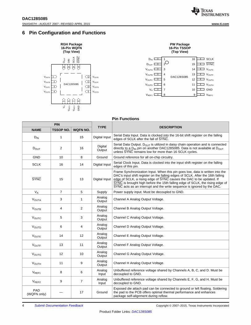
6 Pin Configuration and Functions
RGH Package PW Package16-Pin WQFN 16-Pin TSSOP
(Top View) (Top View)
Pin FunctionsPIN
TYPE DESCRIPTIONNAME TSSOP NO. WQFN NO.
Serial Data Input. Data is clocked into the 16-bit shift register on the fallingDIN 1 15 Digital Input edges of SCLK after the fall of SYNC.Serial Data Output. DOUT is utilized in daisy chain operation and is connectedDigitalDOUT 2 16 directly to a DIN pin on another DAC128S085. Data is not available at DOUTOutput unless SYNC remains low for more than 16 SCLK cycles.
GND 10 8 Ground Ground reference for all on-chip circuitry.Serial Clock Input. Data is clocked into the input shift register on the fallingSCLK 16 14 Digital Input edges of this pin.Frame Synchronization Input. When this pin goes low, data is written into theDAC's input shift register on the falling edges of SCLK. After the 16th falling
SYNC 15 13 Digital Input edge of SCLK, a rising edge of SYNC causes the DAC to be updated. IfSYNC is brought high before the 15th falling edge of SCLK, the rising edge ofSYNC acts as an interrupt and the write sequence is ignored by the DAC.
VA 7 5 Supply Power supply input. Must be decoupled to GND.AnalogVOUTA 3 1 Channel A Analog Output Voltage.OutputAnalogVOUTB 4 2 Channel B Analog Output Voltage.OutputAnalogVOUTC 5 3 Channel C Analog Output Voltage.OutputAnalogVOUTD 6 4 Channel D Analog Output Voltage.OutputAnalogVOUTE 14 12 Channel E Analog Output Voltage.OutputAnalogVOUTF 13 11 Channel F Analog Output Voltage.OutputAnalogVOUTG 12 10 Channel G Analog Output Voltage.OutputAnalogVOUTH 11 9 Channel H Analog Output Voltage.OutputAnalog Unbuffered reference voltage shared by Channels A, B, C, and D. Must beVREF1 8 6 Input decoupled to GND.Analog Unbuffered reference voltage shared by Channels E, F, G, and H. Must beVREF2 9 7 Input decoupled to GND.
Exposed die attach pad can be connected to ground or left floating. SolderingPAD — 17 Ground the pad to the PCB offers optimal thermal performance and enhances(WQFN only) package self-alignment during reflow.
4 Submit Documentation Feedback Copyright © 2007–2015, Texas Instruments Incorporated
Product Folder Links: DAC128S085

I/O
GND
TO INTERNAL
CIRCUITRY
DAC128S085www.ti.com SNAS407H –AUGUST 2007–REVISED APRIL 2015
7 Specifications
7.1 Absolute Maximum Ratingsover operating free-air temperature range (unless otherwise noted) (1) (2)
MIN MAX UNITSupply Voltage, VA 6.5 VVoltage on any Input Pin −0.3 6.5 VInput Current at Any Pin (3) 10 mAPackage Input Current (3) 30 mAPower Consumption at TA = 25°C See (4)
Junction Temperature 150 °CStorage Temperature, Tstg −65 150 °C
(1) Absolute Maximum Ratings indicate limits beyond which damage to the device may occur. Recomended Operating Ratings indicateconditions for which the device is functional, but do not specify specific performance limits. For ensured specifications and testconditions, see Electrical Characteristics. The ensured specifications apply only for the test conditions listed. Some performancecharacteristics may degrade when the device is not operated under the listed test conditions. Operation of the device beyond theAbsolute Maximum Ratings is not recommended.
(2) All voltages are measured with respect to GND = 0 V, unless otherwise specified.(3) When the input voltage at any pin exceeds 5.5 V or is less than GND, the current at that pin should be limited to 10 mA. The 30-mA
maximum package input current rating limits the number of pins that can safely exceed the power supplies with an input current of 10mA to three.
(4) The absolute maximum junction temperature (TJmax) for this device is 150°C. The maximum allowable power dissipation is dictated byTJmax, the junction-to-ambient thermal resistance (RθJA), and the ambient temperature (TA), and can be calculated using the formulaPDMAX = (TJmax − TA) / RθJA. The values for maximum power dissipation will be reached only when the device is operated in a severefault condition (for example, when input or output pins are driven beyond the operating ratings, or the power supply polarity is reversed).Such conditions should always be avoided.
7.2 ESD RatingsVALUE UNIT
Human body model (HBM), per ANSI/ESDA/JEDEC JS-001 (1) ±2500Charged-device model (CDM), per JEDEC specification JESD22- ±1000V(ESD) Electrostatic discharge VC101 (2)
Machine Model ±250
(1) JEDEC document JEP155 states that 500-V HBM allows safe manufacturing with a standard ESD control process.(2) JEDEC document JEP157 states that 250-V CDM allows safe manufacturing with a standard ESD control process.
7.3 Recommended Operating Conditionsover operating free-air temperature range (unless otherwise noted)
MIN MAX UNITOperating Temperature Range −40 ≤ TA ≤ °C
+125Supply Voltage, VA 2.7 5.5 VReference Voltage, VREF1,2 0.5 VA VDigital Input Voltage (1) 0.0 5.5 VOutput Load 0 1500 pFSCLK Frequency 40 MHz
(1) The inputs are protected as shown below. Input voltage magnitudes up to 5.5 V, regardless of VA, will not cause errors in the conversionresult. For example, if VA is 3 V, the digital input pins can be driven with a 5-V logic device.
Copyright © 2007–2015, Texas Instruments Incorporated Submit Documentation Feedback 5
Product Folder Links: DAC128S085
DAC128S085SNAS407H –AUGUST 2007–REVISED APRIL 2015 www.ti.com
7.4 Thermal InformationDAC128S085
THERMAL METRIC (1) PW (TSSOP) RGH (WQFN) UNIT16 PINS 16 PINS
RθJA Junction-to-ambient thermal resistance 98 34RθJA Junction-to-ambient thermal resistance 31 25RθJA Junction-to-ambient thermal resistance 43 11 °C/WφJT Junction-to-top characterization parameter 2 0.2φJB Junction-to-board characterization parameter 43 11
(1) For more information about traditional and new thermal metrics, see the IC Package Thermal Metrics application report, SPRA953.
7.5 Electrical CharacteristicsThe following specifications apply for VA = 2.7 V to 5.5 V, VREF1 = VREF2 = VA, CL = 200 pF to GND, fSCLK = 30 MHz, inputcode range 48 to 4047. All limits are at TA = 25°C, unless otherwise specified.
PARAMETER TEST CONDITIONS MIN (1) TYP MAX (1) UNITSTATIC PERFORMANCE
Resolution TMIN ≤ TA ≤ TMAX 12 BitsMonotonicity TMIN ≤ TA ≤ TMAX 12 Bits
±2INL Integral Non-Linearity LSB
TMIN ≤ TA ≤ TMAX ±80.15 LSB
TMIN ≤ TA ≤ TMAX 0.75DNL Differential Non-Linearity
−0.09 LSBTMIN ≤ TA ≤ TMAX −0.4IOUT = 0 +5
ZE Zero Code Error mVTMIN ≤ TA ≤ TMAX 15IOUT = 0 −0.1%
FSE Full-Scale Error FSRTMIN ≤ TA ≤ TMAX −0.75%
−0.2%GE Gain Error FSR
TMIN ≤ TA ≤ TMAX −1 %ZCED Zero Code Error Drift −20 µV/°CTC GE Gain Error Tempco −1 ppm/°COUTPUT CHARACTERISTICS
Output Voltage Range TMIN ≤ TA ≤ TMAX 0 VREF1,2 VHigh-Impedance OutputIOZ TMIN ≤ TA ≤ TMAX ±1 µALeakage Current (2)
VA = 3 V, IOUT = 200 µA 10 mVVA = 3 V, IOUT = 1 mA 45 mV
ZCO Zero Code OutputVA = 5 V, IOUT = 200 µA 8 mVVA = 5 V, IOUT = 1 mA 34 mVVA = 3 V, IOUT = 200 µA 2.984 VVA = 3 V, IOUT = 1 mA 2.933 V
FSO Full Scale OutputVA = 5 V, IOUT = 200 µA 4.987 VVA = 5 V, IOUT = 1 mA 4.955 V
(1) Test limits are ensured to TI's AOQL (Average Outgoing Quality Level).(2) This parameter is ensured by design and/or characterization and is not tested in production.
6 Submit Documentation Feedback Copyright © 2007–2015, Texas Instruments Incorporated
Product Folder Links: DAC128S085

DAC128S085www.ti.com SNAS407H –AUGUST 2007–REVISED APRIL 2015
Electrical Characteristics (continued)The following specifications apply for VA = 2.7 V to 5.5 V, VREF1 = VREF2 = VA, CL = 200 pF to GND, fSCLK = 30 MHz, inputcode range 48 to 4047. All limits are at TA = 25°C, unless otherwise specified.
PARAMETER TEST CONDITIONS MIN (1) TYP MAX (1) UNITVA = 3 V, VOUT = 0 V, −50 mAInput Code = FFFhOutput Short Circuit CurrentIOS (source) (3) VA = 5 V, VOUT = 0 V, −60 mAInput Code = FFFhVA = 3 V, VOUT = 3 V, 50 mAInput Code = 000hOutput Short Circuit CurrentIOS (sink) (3) VA = 5 V, VOUT = 5 V, 70 mAInput Code = 000hTA = 105°C 10 mATMIN ≤ TA ≤ TMAXContinuous Output Current perIO channel (2) TA = 125°C 6.5 mATMIN ≤ TA ≤ TMAX
RL = ∞ 1500 pFCL Maximum Load Capacitance
RL = 2 kΩ 1500 pFZOUT DC Output Impedance 8 ΩREFERENCE INPUTCHARACTERISTICS
0.5Input Range Minimum V
TMIN ≤ TA ≤ TMAX 2.7VREF1,2
Input Range Maximum TMIN ≤ TA ≤ TMAX VA VInput Impedance 30 kΩ
LOGIC INPUT CHARACTERISTICSIIN Input Current (2) TMIN ≤ TA ≤ TMAX ±1 µA
VA = 2.7 V to 3.6 V 1V
TMIN ≤ TA ≤ TMAX 0.6VIL Input Low Voltage
VA = 4.5 V to 5.5 V 1.1V
0.8VA = 2.7 V to 3.6 V 1.4
VTMIN ≤ TA ≤ TMAX 2.1
VIH Input High VoltageVA = 4.5 V to 5.5 V 2
VTMIN ≤ TA ≤ TMAX 2.4
CIN Input Capacitance (2) TMIN ≤ TA ≤ TMAX 3 pF
(3) This parameter does not represent a condition which the DAC can sustain continuously. See the continuous output current specificationfor the maximum DAC output current per channel.
Copyright © 2007–2015, Texas Instruments Incorporated Submit Documentation Feedback 7
Product Folder Links: DAC128S085

DAC128S085SNAS407H –AUGUST 2007–REVISED APRIL 2015 www.ti.com
Electrical Characteristics (continued)The following specifications apply for VA = 2.7 V to 5.5 V, VREF1 = VREF2 = VA, CL = 200 pF to GND, fSCLK = 30 MHz, inputcode range 48 to 4047. All limits are at TA = 25°C, unless otherwise specified.
PARAMETER TEST CONDITIONS MIN (1) TYP MAX (1) UNITPOWER REQUIREMENTS
Supply Voltage Minimum TMIN ≤ TA ≤ TMAX 2.7 VVA Supply Voltage Maximum TMIN ≤ TA ≤ TMAX 5.5 V
VA = 2.7 V to 4603.6 VµA
TMIN ≤ TA ≤ 560Normal Supply Current for fSCLK = 30 MHz, TMAXsupply pin VA output unloadedVA = 4.5 V to 6505.5 V µA
830IN VA = 2.7 V to 953.6 V
µATMIN ≤ TA ≤ 130Normal Supply Current for fSCLK = 30 MHz, TMAXVREF1 or VREF2 output unloadedVA = 4.5 V to 1605.5 V µA
220VA = 2.7 V to 370 µA3.6 VStatic Supply Current for fSCLK = 0,
supply pin VA output unloaded VA = 4.5 V to 440 µA5.5 VIST VA = 2.7 V to 95 µA3.6 VStatic Supply Current for fSCLK = 0,
VREF1 or VREF2 output unloaded VA = 4.5 V to 160 µA5.5 VVA = 2.7 V to 0.23.6 V µA
fSCLK = 30 MHz, 1.5SYNC = VA and
VA = 4.5 V toDIN = 0V after PD 0.55.5 Vmode loaded µATMIN ≤ TA ≤ 3TMAXTotal Power Down Supply
IPD Current for all PD Modes VA = 2.7 V to 0.1(2) 3.6 VµA
TMIN ≤ TA ≤fSCLK = 0, SYNC = 1TMAXVA and DIN = 0Vafter PD mode VA = 4.5 V to 0.2loaded 5.5 V
µATMIN ≤ TA ≤ 2TMAX
VA = 2.7 V to 1.953.6 VmW
TMIN ≤ TA ≤ 3TMAXfSCLK = 30 MHzoutput unloaded VA = 4.5 V to 4.855.5 VTotal Power ConsumptionPN mW(output unloaded) TMIN ≤ TA ≤ 7TMAX
VA = 2.7 V to 1.68 mW3.6 VfSCLK = 0output unloaded VA = 4.5 V to 3.80 mW5.5 V
8 Submit Documentation Feedback Copyright © 2007–2015, Texas Instruments Incorporated
Product Folder Links: DAC128S085

DAC128S085www.ti.com SNAS407H –AUGUST 2007–REVISED APRIL 2015
Electrical Characteristics (continued)The following specifications apply for VA = 2.7 V to 5.5 V, VREF1 = VREF2 = VA, CL = 200 pF to GND, fSCLK = 30 MHz, inputcode range 48 to 4047. All limits are at TA = 25°C, unless otherwise specified.
PARAMETER TEST CONDITIONS MIN (1) TYP MAX (1) UNITVA = 2.7 V to 0.63.6 V
µWTMIN ≤ TA ≤fSCLK = 30 MHz, 5.4TMAXSYNC = VA and
DIN = 0V after PD VA = 4.5V to 2.5mode loaded 5.5VµW
TMIN ≤ TA ≤ 16.5Total Power Consumption in TMAXPPD all PD Modes,VA = 2.7 V to(2) 0.33.6 V
µWTMIN ≤ TA ≤fSCLK = 0, SYNC = 3.6TMAXVA and DIN = 0V
after PD mode VA = 4.5 V to 1loaded 5.5 VµW
TMIN ≤ TA ≤ 11TMAX
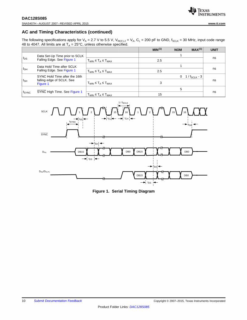
7.6 AC and Timing CharacteristicsThe following specifications apply for VA = 2.7 V to 5.5 V, VREF1,2 = VA, CL = 200 pF to GND, fSCLK = 30 MHz, input code range48 to 4047. All limits are at TA = 25°C, unless otherwise specified.
MIN (1) NOM MAX (1) UNIT40
fSCLK SCLK Frequency MHzTMIN ≤ TA ≤ TMAX 30400h to C00h code change 6Output Voltage Settling Time RL = 2 kΩ, CL = 200 pFts µs(2)TMIN ≤ TA ≤ TMAX 8.5
SR Output Slew Rate 1 V/µsGI Glitch Impulse Code change from 800h to 7FFh 40 nV-secDF Digital Feedthrough 0.5 nV-secDC Digital Crosstalk 0.5 nV-secCROSS DAC-to-DAC Crosstalk 1 nV-secMBW Multiplying Bandwidth VREF1,2 = 2.5 V ± 2 Vpp 360 kHz
Total Harmonic Distortion Plus VREF1,2 = 2.5 V ± 0.5 VppTHD+N −80 dBNoise 100 Hz < fIN < 20 kHzONSD Output Noise Spectral Density DAC Code = 800 h, 10 kHz 40 nV/sqrt (Hz)ON Output Noise BW = 30 kHz 14 µV
VA = 3 V 3 µsectWU Wake-Up Time
VA = 5 V 20 µsec25
1/fSCLK SCLK Cycle Time. See Figure 1 nsTMIN ≤ TA ≤ TMAX 33
7tCH SCLK High time. See Figure 1 ns
TMIN ≤ TA ≤ TMAX 107
tCL SCLK Low Time. See Figure 1 nsTMIN ≤ TA ≤ TMAX 10
3 1 / fSCLK - 3SYNC Set-up Time prior totSS nsSCLK Falling Edge. See Figure 1 TMIN ≤ TA ≤ TMAX 10
(1) Test limits are ensured to TI's AOQL (Average Outgoing Quality Level).(2) This parameter is ensured by design and/or characterization and is not tested in production.
Copyright © 2007–2015, Texas Instruments Incorporated Submit Documentation Feedback 9
Product Folder Links: DAC128S085
DB15
SCLK
DIN1
SYNC
tDS
tDH
||
|
1 2 15 16
DB15 DB0
DIN2/DOUT1
tDS
||
DB0 DB0
||
||
tDH
|
tSYNCtSS tCL tCH
tSH
1 / fSCLK
|
1 2 15 16
DB15
DAC128S085SNAS407H –AUGUST 2007–REVISED APRIL 2015 www.ti.com
AC and Timing Characteristics (continued)The following specifications apply for VA = 2.7 V to 5.5 V, VREF1,2 = VA, CL = 200 pF to GND, fSCLK = 30 MHz, input code range48 to 4047. All limits are at TA = 25°C, unless otherwise specified.
MIN (1) NOM MAX (1) UNIT1Data Set-Up Time prior to SCLKtDS nsFalling Edge. See Figure 1 TMIN ≤ TA ≤ TMAX 2.51Data Hold Time after SCLKtDH nsFalling Edge. See Figure 1 TMIN ≤ TA ≤ TMAX 2.5
SYNC Hold Time after the 16th 0 1 / fSCLK - 3tSH falling edge of SCLK. See ns
TMIN ≤ TA ≤ TMAX 3Figure 15
tSYNC SYNC High Time. See Figure 1 nsTMIN ≤ TA ≤ TMAX 15
Figure 1. Serial Timing Diagram
10 Submit Documentation Feedback Copyright © 2007–2015, Texas Instruments Incorporated
Product Folder Links: DAC128S085

DAC128S085www.ti.com SNAS407H –AUGUST 2007–REVISED APRIL 2015
7.7 Typical CharacteristicsVA = 2.7 V to 5.5 V, VREF1,2 = VA, fSCLK = 30 MHz, TA = 25°C, unless otherwise stated
Figure 2. INL vs Code Figure 3. DNL vs Code
Figure 4. INL / DNL vs VREF Figure 5. INL / DNL vs FSCLK
Figure 6. INL / DNL vs VA Figure 7. INL / DNL vs Temperature
Copyright © 2007–2015, Texas Instruments Incorporated Submit Documentation Feedback 11
Product Folder Links: DAC128S085
DAC128S085SNAS407H –AUGUST 2007–REVISED APRIL 2015 www.ti.com
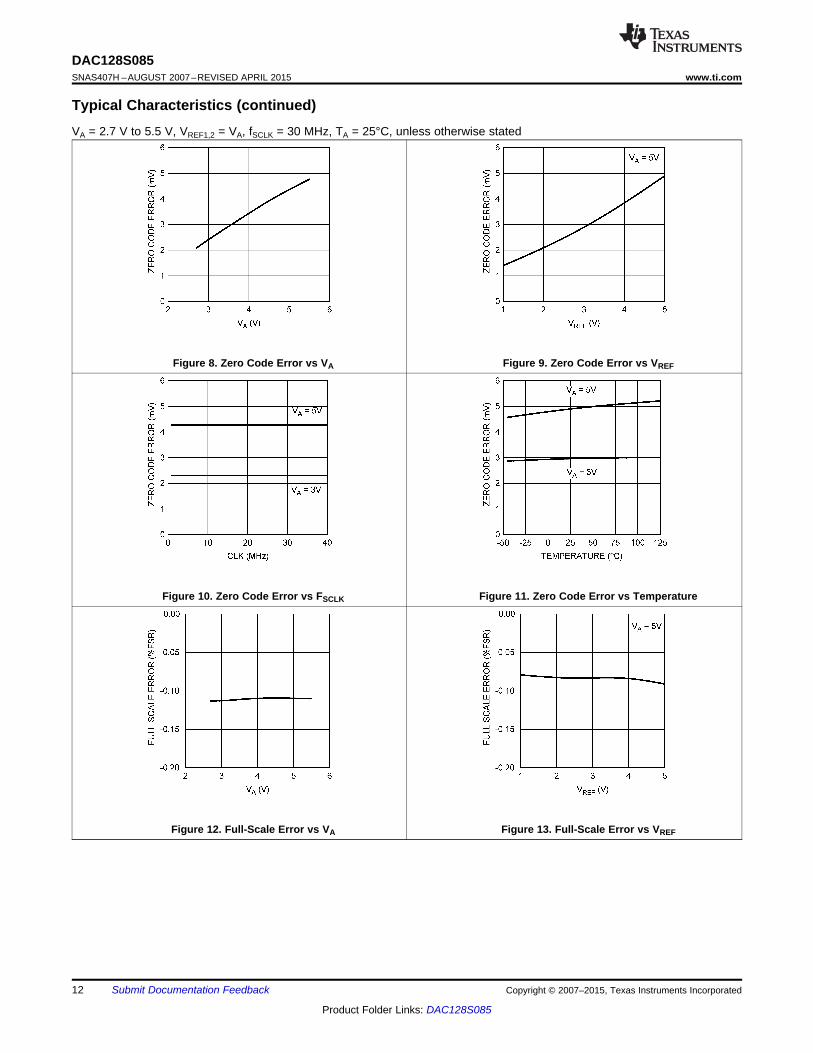
Typical Characteristics (continued)VA = 2.7 V to 5.5 V, VREF1,2 = VA, fSCLK = 30 MHz, TA = 25°C, unless otherwise stated
Figure 8. Zero Code Error vs VA Figure 9. Zero Code Error vs VREF
Figure 10. Zero Code Error vs FSCLK Figure 11. Zero Code Error vs Temperature
Figure 12. Full-Scale Error vs VA Figure 13. Full-Scale Error vs VREF
12 Submit Documentation Feedback Copyright © 2007–2015, Texas Instruments Incorporated
Product Folder Links: DAC128S085
DAC128S085www.ti.com SNAS407H –AUGUST 2007–REVISED APRIL 2015
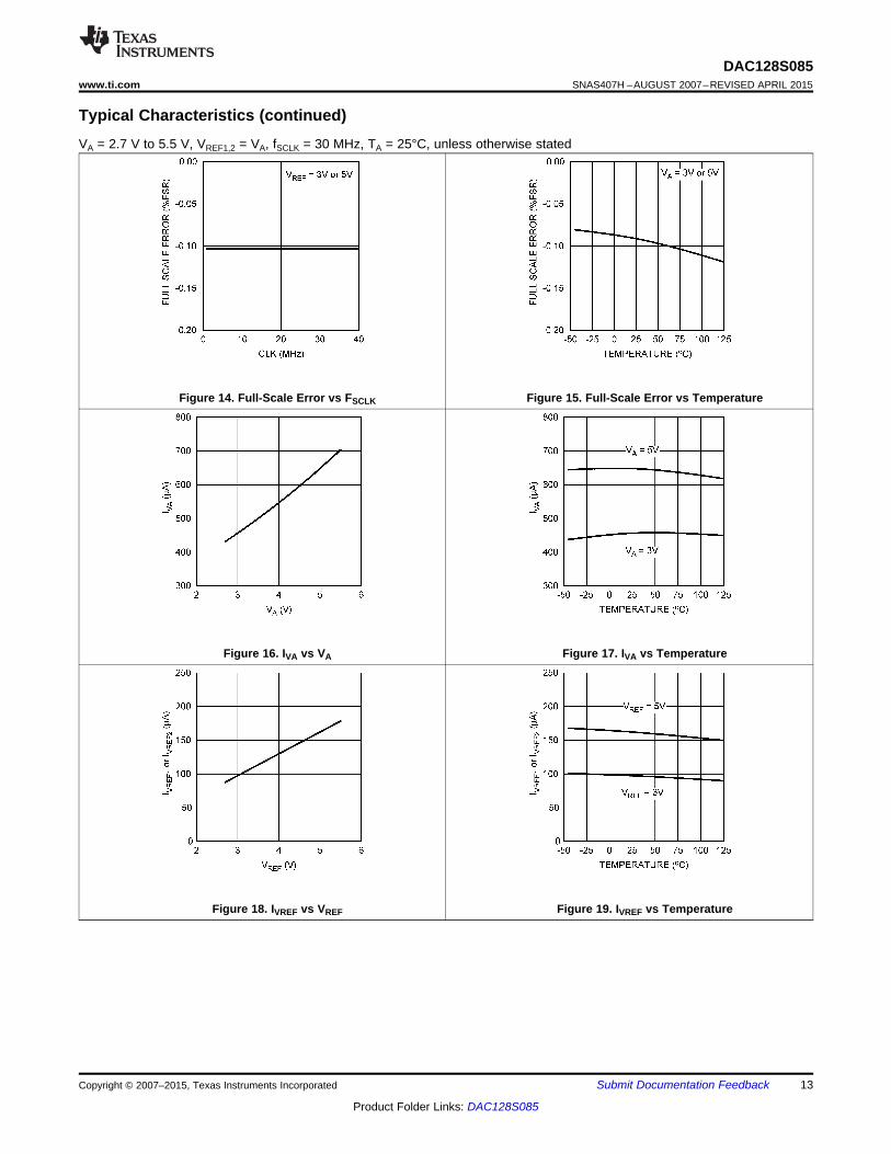
Typical Characteristics (continued)VA = 2.7 V to 5.5 V, VREF1,2 = VA, fSCLK = 30 MHz, TA = 25°C, unless otherwise stated
Figure 14. Full-Scale Error vs FSCLK Figure 15. Full-Scale Error vs Temperature
Figure 16. IVA vs VA Figure 17. IVA vs Temperature
Figure 18. IVREF vs VREF Figure 19. IVREF vs Temperature
Copyright © 2007–2015, Texas Instruments Incorporated Submit Documentation Feedback 13
Product Folder Links: DAC128S085
DAC128S085SNAS407H –AUGUST 2007–REVISED APRIL 2015 www.ti.com
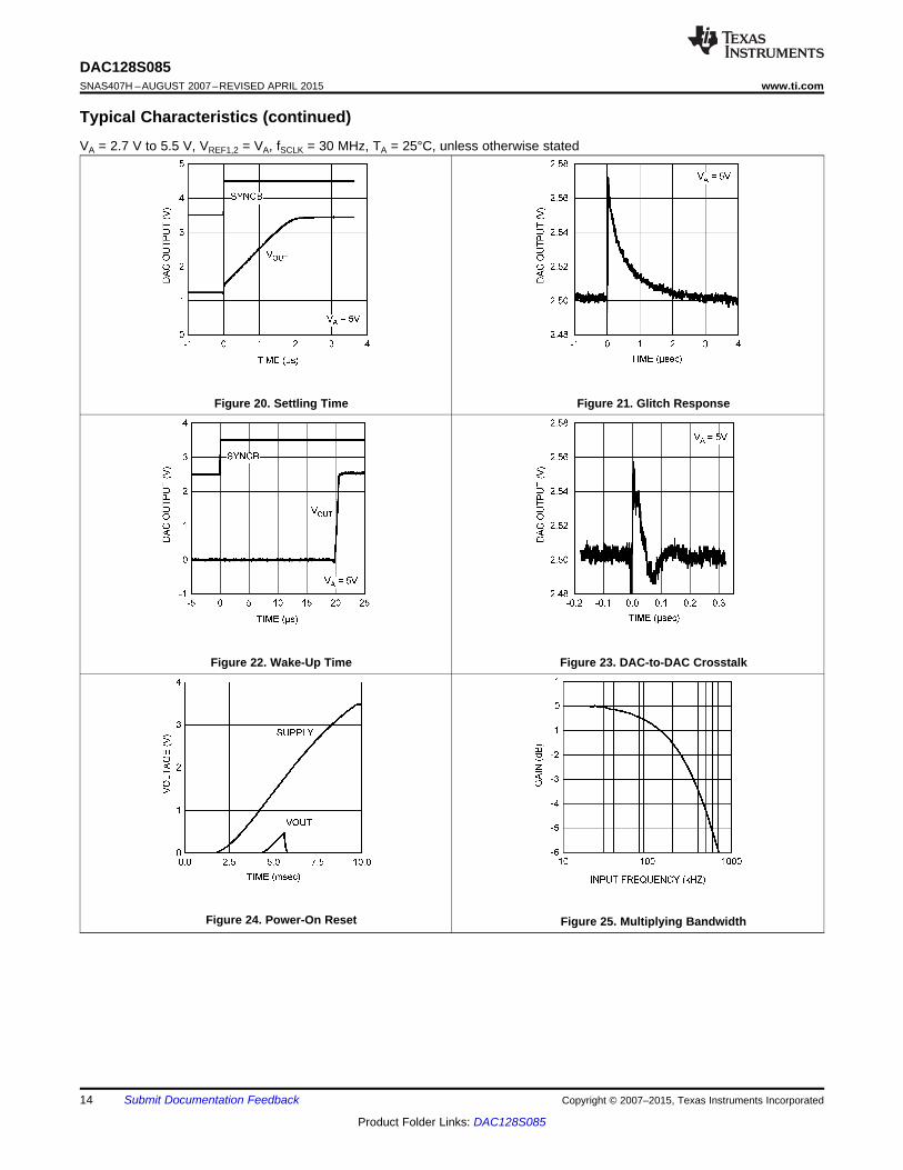
Typical Characteristics (continued)VA = 2.7 V to 5.5 V, VREF1,2 = VA, fSCLK = 30 MHz, TA = 25°C, unless otherwise stated
Figure 20. Settling Time Figure 21. Glitch Response
Figure 22. Wake-Up Time Figure 23. DAC-to-DAC Crosstalk
Figure 24. Power-On Reset Figure 25. Multiplying Bandwidth
14 Submit Documentation Feedback Copyright © 2007–2015, Texas Instruments Incorporated
Product Folder Links: DAC128S085

POWER-ONRESET
DACREGISTER
INPUTCONTROL
LOGIC
12
POWER-DOWNCONTROL
LOGIC
VOUTE12 BIT DAC
REF
12
SCLK DINSYNC
BUFFER
BUFFER
BUFFER
BUFFER
12
12
12
VOUTF
VOUTG
VOUTH
2.5k 100k
2.5k 100k
2.5k 100k
2.5k 100k
12 BIT DAC
REF
12 BIT DAC
REF
12 BIT DAC
REF
VREF1
DAC128S085
VOUTA12 BIT DAC
REF
12
BUFFER
BUFFER
BUFFER
BUFFER
12
12
12
VOUTB
VOUTC
VOUTD
2.5k 100k
2.5k 100k
2.5k 100k
2.5k 100k
12 BIT DAC
REF
12 BIT DAC
REF
12 BIT DAC
REF
VREF2DOUT
DAC128S085www.ti.com SNAS407H –AUGUST 2007–REVISED APRIL 2015
8 Detailed Description
8.1 OverviewThe DAC128S085 is fabricated on a CMOS process with an architecture that consists of switches and resistorstrings followed by an output buffer. The reference voltages are externally applied at VREF1 for DAC channels Athrough D, and VREF2 for DAC channels E through H.
8.2 Functional Block Diagram
Copyright © 2007–2015, Texas Instruments Incorporated Submit Documentation Feedback 15
Product Folder Links: DAC128S085

VOUT
12 BIT DAC
REF
12BUFFERDAC
REGISTER
VREF
VREF
VOUT
R
R
R
R
R
S0
S1
S2
S2 n
S2 n-1
S2 n-2
DAC128S085SNAS407H –AUGUST 2007–REVISED APRIL 2015 www.ti.com
8.3 Feature Description
8.3.1 DAC ArchitectureFor simplicity, a single resistor string is shown in Figure 26. This string consists of 4096 equal valued resistorswith a switch at each junction of two resistors, plus a switch to ground. The code loaded into the DAC registerdetermines which switch is closed, connecting the proper node to the amplifier. The input coding is straightbinary with an ideal output voltage of:
VOUTA,B,C,D = VREF1 × (D / 4096)
where• D is the decimal equivalent of the binary code that is loaded into the DAC register. (1)
VOUTE,F,G,H = VREF2 × (D / 4096) (2)
D can take on any value between 0 and 4095. This configuration ensures that the DAC is monotonic.
Figure 26. DAC Resistor String
Because all eight DAC channels of the DAC128S085 can be controlled independently, each channel consists ofa DAC register and a 12-bit DAC. Figure 27 is a simple block diagram of an individual channel in theDAC128S085. Depending on the mode of operation, data written into a DAC register causes the 12-bit DACoutput to be updated, or an additional command is required to update the DAC output. Further description of themodes of operation can be found in Serial Interface.
Figure 27. Single-Channel Block Diagram
16 Submit Documentation Feedback Copyright © 2007–2015, Texas Instruments Incorporated
Product Folder Links: DAC128S085

SCLK
SYNC
tSS
1 17
tSH
1615
DAC128S085www.ti.com SNAS407H –AUGUST 2007–REVISED APRIL 2015
Feature Description (continued)8.3.2 Output AmplifiersThe output amplifiers are rail-to-rail, providing an output voltage range of 0 V to VA when the reference is VA. Allamplifiers, including rail-to-rail types, exhibit a loss of linearity as the output approaches the supply rails (0 V andVA, in this case). For this reason, linearity is specified over less than the full output range of the DAC. However, ifthe reference is less than VA, only the lowest codes experience a loss in linearity.
The output amplifiers can drive a load of 2 kΩ in parallel with 1500 pF to ground or to VA. The zero-code and full-scale outputs for given load currents are available in the Electrical Characteristics.
8.3.3 Reference VoltageThe DAC128S085 uses dual external references, VREF1 and VREF2, which are shared by channels A, B, C, D andchannels E, F, G, H, respectively. The reference pins are not buffered and have an input impedance of 30 kΩ. TIrecommends driving VREF1 and VREF2 by voltage sources with low output impedance. The reference voltagerange is 0.5 V to VA, providing the widest possible output dynamic range.
8.3.4 Serial InterfaceThe three-wire interface is compatible with SPI, QSPI, and MICROWIRE, as well as most DSPs, and operates atclock rates up to 40 MHz. A valid serial frame contains 16 falling edges of SCLK. See Table 1 for information ona write sequence.
A write sequence begins by bringing the SYNC line low. Once SYNC is low, the data on the DIN line is clockedinto the 16-bit serial input register on the falling edges of SCLK. To avoid mis-clocking data into the shift register,it is critical that SYNC not be brought low on a falling edge of SCLK (see minimum and maximum setup times forSYNC in AC and Timing Characteristics and Figure 28). On the 16th falling edge of SCLK, the last data bit isclocked into the register. The write sequence is concluded by bringing the SYNC line high. Once SYNC is high,the programmed function (a change in the DAC channel address, mode of operation, or register contents) isexecuted. To avoid mis-clocking data into the shift register, it is critical that SYNC be brought high between the16th and 17th falling edges of SCLK (see minimum and maximum hold times for SYNC in AC and TimingCharacteristics and Figure 28).
Figure 28. CS Setup and Hold Times
If SYNC is brought high before the 15th falling edge of SCLK, the write sequence is aborted and the data thathas been shifted into the input register is discarded. If SYNC is held low beyond the 17th falling edge of SCLK,the serial data presented at DIN will begin to be output on DOUT. More information on this mode of operation canbe found in Daisy-Chain Operation. In either case, SYNC must be brought high for the minimum specified timebefore the next write sequence is initiated with a falling edge of SYNC.
Since the DIN buffer draws more current when it is high, it should be idled low between write sequences tominimize power consumption. On the other hand, SYNC should be idled high to avoid the activation of daisychain operation where DOUT is active.
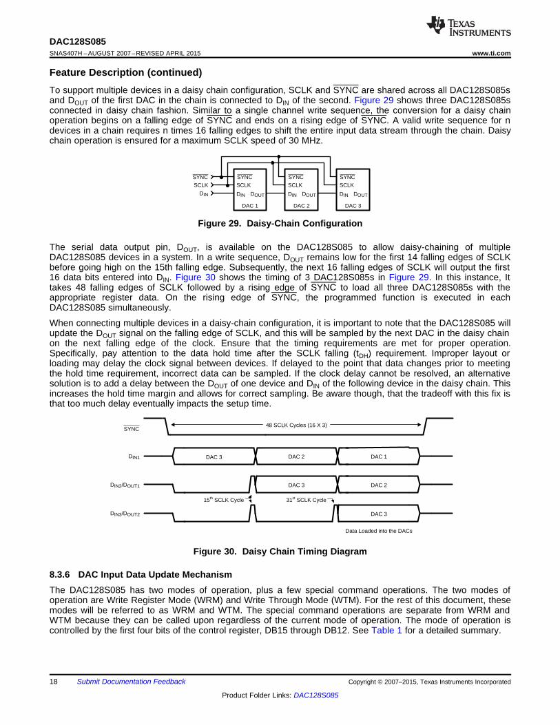
8.3.5 Daisy-Chain OperationDaisy-chain operation allows communication with any number of DAC128S085s using a single serial interface.As long as the correct number of data bits are input in a write sequence (multiple of sixteen bits), a rising edge ofSYNC will properly update all DACs in the system.
Copyright © 2007–2015, Texas Instruments Incorporated Submit Documentation Feedback 17
Product Folder Links: DAC128S085
DAC 3DIN1
SYNC
DAC 2 DAC 1
DAC 3 DAC 2
DAC 3
DIN2/DOUT1
DIN3/DOUT2
Data Loaded into the DACs
48 SCLK Cycles (16 X 3)
15th SCLK Cycle 31st SCLK Cycle
DAC 1
SCLK
DIN
SYNC
DOUT
DAC 2
SCLK
DIN
SYNC
DOUT
DAC 3
SCLK
DIN
SYNC
DOUT
SCLK
DIN
SYNC
DAC128S085SNAS407H –AUGUST 2007–REVISED APRIL 2015 www.ti.com
Feature Description (continued)To support multiple devices in a daisy chain configuration, SCLK and SYNC are shared across all DAC128S085sand DOUT of the first DAC in the chain is connected to DIN of the second. Figure 29 shows three DAC128S085sconnected in daisy chain fashion. Similar to a single channel write sequence, the conversion for a daisy chainoperation begins on a falling edge of SYNC and ends on a rising edge of SYNC. A valid write sequence for ndevices in a chain requires n times 16 falling edges to shift the entire input data stream through the chain. Daisychain operation is ensured for a maximum SCLK speed of 30 MHz.
Figure 29. Daisy-Chain Configuration
The serial data output pin, DOUT, is available on the DAC128S085 to allow daisy-chaining of multipleDAC128S085 devices in a system. In a write sequence, DOUT remains low for the first 14 falling edges of SCLKbefore going high on the 15th falling edge. Subsequently, the next 16 falling edges of SCLK will output the first16 data bits entered into DIN. Figure 30 shows the timing of 3 DAC128S085s in Figure 29. In this instance, Ittakes 48 falling edges of SCLK followed by a rising edge of SYNC to load all three DAC128S085s with theappropriate register data. On the rising edge of SYNC, the programmed function is executed in eachDAC128S085 simultaneously.
When connecting multiple devices in a daisy-chain configuration, it is important to note that the DAC128S085 willupdate the DOUT signal on the falling edge of SCLK, and this will be sampled by the next DAC in the daisy chainon the next falling edge of the clock. Ensure that the timing requirements are met for proper operation.Specifically, pay attention to the data hold time after the SCLK falling (tDH) requirement. Improper layout orloading may delay the clock signal between devices. If delayed to the point that data changes prior to meetingthe hold time requirement, incorrect data can be sampled. If the clock delay cannot be resolved, an alternativesolution is to add a delay between the DOUT of one device and DIN of the following device in the daisy chain. Thisincreases the hold time margin and allows for correct sampling. Be aware though, that the tradeoff with this fix isthat too much delay eventually impacts the setup time.
Figure 30. Daisy Chain Timing Diagram
8.3.6 DAC Input Data Update MechanismThe DAC128S085 has two modes of operation, plus a few special command operations. The two modes ofoperation are Write Register Mode (WRM) and Write Through Mode (WTM). For the rest of this document, thesemodes will be referred to as WRM and WTM. The special command operations are separate from WRM andWTM because they can be called upon regardless of the current mode of operation. The mode of operation iscontrolled by the first four bits of the control register, DB15 through DB12. See Table 1 for a detailed summary.
18 Submit Documentation Feedback Copyright © 2007–2015, Texas Instruments Incorporated
Product Folder Links: DAC128S085
DAC128S085www.ti.com SNAS407H –AUGUST 2007–REVISED APRIL 2015
Feature Description (continued)Table 1. Write Register and Write Through Modes
DB[15:12] DB[11:0] Description of ModeWRM: The registers of each DAC Channel can be written to without causing1 0 0 0 X X X X X X X X X X X X their outputs to change.
1 0 0 1 X X X X X X X X X X X X WTM: Writing data to a channel's register causes the DAC output to change.
When the DAC128S085 first powers up, the DAC is in WRM. In WRM, the registers of each individual DACchannel can be written to without updating the DAC outputs. This is accomplished by setting DB15 to 0,specifying the DAC register to be written to in DB[14:12], and entering the new DAC register setting in DB[11:0](see Table 2). The DAC128S085 remains in WRM until the mode of operation is changed to WTM. The mode ofoperation is changed from WRM to WTM by setting DB[15:12] to 1001. Once in WTM, writing data to a DACchannel register causes the DAC output to be updated as well. Changing a DAC channel register in WTM isaccomplished in the same manner as in WRM. However, in WTM the DAC register and output are updated at thecompletion of the command (see Table 2). Similarly, the DAC128S085 remains in WTM until the mode ofoperation is changed to WRM by setting DB[15:12] to 1000.
Table 2. Commands Impacted by WRM and WTMDB15 DB[14:12] DB[11:0] Description of Mode
WRM: D[11:0] written to ChA's data register only0 0 0 0 D11 D10 ... D1 D0 WTM: ChA's output is updated by data in D[11:0]WRM: D[11:0] written to only the data register of ChB0 0 0 1 D11 D10 ... D1 D0 WTM: ChB's output is updated by data in D[11:0]WRM: D[11:0] written to only the data register of ChC0 0 1 0 D11 D10 ... D1 D0 WTM: ChC's output is updated by data in D[11:0]WRM: D[11:0] written only the data register of ChD0 0 1 1 D11 D10 ... D1 D0 WTM: ChD's output is updated by data in D[11:0]WRM: D[11:0] written only the data register of ChE0 1 0 0 D11 D10 ... D1 D0 WTM: ChE's output is updated by data in D[11:0]WRM: D[11:0] written only the data register of ChF0 1 0 1 D11 D10 ... D1 D0 WTM: ChF's output is updated by data in D[11:0]WRM: D[11:0] written only the data register of ChG0 1 1 0 D11 D10 ... D1 D0 WTM: ChG's output is updated by data in D[11:0]WRM: D[11:0] written only the data register of ChH0 1 1 1 D11 D10 ... D1 D0 WTM: ChH's output is updated by data in D[11:0]
The special command operations can be exercised at any time regardless of the mode of operation. There arethree special command operations. The first command is exercised by setting data bits DB[15:12] to 1010. Thisallows the user to update multiple DAC outputs simultaneously to the values currently loaded in their respectivecontrol registers. This command is valuable if the user wants each DAC output to be at a different output voltage,but still have all the DAC outputs changed to their appropriate values simultaneously (see Table 3).
The second special command allows the user to alter the DAC output of channel A with a single write frame.This command is exercised by setting data bits DB[15:12] to 1011 and data bits DB[11:0] to the desired controlregister value. This command also causes the DAC outputs of the other channels to update to their currentcontrol register values. The user may choose to exercise this command to save a write sequence. For example,the user may wish to update several DAC outputs simultaneously, including channel A. To accomplish this taskin the minimum number of write frames, the user would alter the control register values of all the DAC channelsexcept channel A while operating in WRM. The last write frame would be used to exercise the special commandChannel A Write Mode. In addition to updating the control register of channel A and output to a new value, all ofthe other channels would be updated as well. At the end of this sequence of write frames, the DAC128S085would still be operating in WRM (see Table 3).
Copyright © 2007–2015, Texas Instruments Incorporated Submit Documentation Feedback 19
Product Folder Links: DAC128S085

OUTPUT
VOLTAGE
DIGITAL INPUT CODE
0
0 4095
ZE
FSE
GE = FSE - ZE
FSE = GE + ZE
4095 x VA
4096
DAC128S085SNAS407H –AUGUST 2007–REVISED APRIL 2015 www.ti.com
The third special command allows the user to set all the DAC control registers and outputs to the same level.This command is commonly referred to as "broadcast" mode, as the same data bits are being broadcast to all ofthe channels simultaneously. This command is exercised by setting data bits DB[15:12] to 1100 and data bitsDB[11:0] to the value that the user wishes to broadcast to all the DAC control registers. Once the command isexercised, each DAC output is updated by the new control register value. This command is frequently used to setall the DAC outputs to some known voltage such as 0 V, VREF/2, or Full Scale. A summary of the commands canbe found in Table 3.
Table 3. Special Command OperationsDB[15:12] DB[11:0] Description of Mode
Update Select: The DAC outputs of the channels selected with a 1 in DB[7:0]1 0 1 0 X X X X H G F E D C B A are updated simultaneously to the values in their respective control registers.Channel A Write: The control register and DAC output of channel A are
1 0 1 1 D11 D10 ... D1 D0 updated to the data in DB[11:0]. The outputs of the other seven channels arealso updated according to their respective control register values.Broadcast: The data in DB[11:0] is written to all channel control registers and1 1 0 0 D11 D10 ... D1 D0 DAC output simultaneously.
8.3.7 Power-On ResetThe power-on reset circuit controls the output voltages of the eight DACs during power-up. Upon application ofpower, the DAC registers are filled with zeros and the output voltages are set to 0 V. The outputs remain at 0 Vuntil a valid write sequence is made.
8.3.8 Transfer Characteristic
Figure 31. Input / Output Transfer Characteristic
8.4 Device Functional Modes
8.4.1 Power-Down ModesThe DAC128S085 has three power-down modes, where different output terminations can be selected (seeTable 4). With all channels powered down, the supply current drops to 0.1 µA at 3 V and 0.2 µA at 5 V. Byselecting the channels to be powered down in DB[7:0] with a 1, individual channels can be powered downseparately, or multiple channels can be powered down simultaneously. The three different output terminationsinclude high output impedance, 100 kΩ to ground, and 2.5 kΩ to ground.
20 Submit Documentation Feedback Copyright © 2007–2015, Texas Instruments Incorporated
Product Folder Links: DAC128S085

DAC128S085www.ti.com SNAS407H –AUGUST 2007–REVISED APRIL 2015
Device Functional Modes (continued)The output amplifiers, resistor strings, and other linear circuitry are all shut down in any of the power-downmodes. The bias generator, however, is only shut down if all the channels are placed in power-down mode. Thecontents of the DAC registers are unaffected when in power-down. Therefore, each DAC register maintains itsvalue prior to the DAC128S085 being powered down unless it is changed during the write sequence thatinstructed it to recover from power down. Minimum power consumption is achieved in the power-down mode withSYNC idled high, DIN idled low, and SCLK disabled. The time to exit power-down (Wake-Up Time) is typically 3µsec at 3 V and 20 µsec at 5 V.
Table 4. Power-Down ModesDB[15:12] DB[11:8] 7 6 5 4 3 2 1 0 Output Impedance
1 1 0 1 X X X X H G F E D C B A Hi-Z outputs1 1 1 0 X X X X H G F E D C B A 100 kΩ outputs1 1 1 1 X X X X H G F E D C B A 2.5 kΩ outputs
8.5 Programming
8.5.1 Programming the DAC128S085This section presents the step-by-step instructions for programming the serial input register.
8.5.1.1 Updating DAC Outputs SimultaneouslyWhen the DAC128S085 is first powered on, the DAC is operating in Write Register Mode (WRM). Operating inWRM allows the user to program the registers of multiple DAC channels without causing the DAC outputs to beupdated. For example, below are the steps for setting Channel A to a full scale output, Channel B to three-quarters full scale, Channel C to half-scale, Channel D to one-quarter full scale and having all the DAC outputsupdate simultaneously.
As stated previously, the DAC128S085 powers up in WRM. If the device was previously operating in WriteThrough Mode (WTM), an extra step to set the DAC into WRM is required. First, the DAC registers must beprogrammed to the desired values. To set Channel A to an output of full scale, write 0FFF to the control register.This updates the data register for Channel A without updating the output of Channel A. Second, set Channel B toan output of three-quarters full scale by writing 1C00 to the control register. This updates the data register forChannel B. Once again, the output of Channel B and Channel A are not updated, because the DAC is operatingin WRM. Third, set Channel C to half scale by writing 2800 to the control register. Fourth, set Channel D to one-quarter full scale by writing 3400 to the control register. Finally, update all four DAC channels simultaneously bywriting A00F to the control register. This procedure allows the user to update four channels simultaneously withfive steps.
Because Channel A was one of the DACs to be updated, one command step could have been saved by writingto Channel A last. Do this by writing to Channel B, C, and D first, and using the the special command Channel AWrite to update the DAC register and output of Channel A. This special command also updates all DAC outputswhile updating Channel A. With this sequence of commands, the user can update four channels simultaneouslyusing four steps. A summary of this command can be found in Table 3.
8.5.1.2 Updating DAC Outputs IndependentlyIf the DAC128S085 is currently operating in WRM, change the mode of operation to WTM by writing 9XXX to thecontrol register. Once the DAC is operating in WTM, any DAC channel can be updated in one step. For example,if a design required Channel G to be set to half scale, the user can write 6800 to the control register to updatethe data register and DAC output of Channel G. Similarly, write 5FFF to the control register to set the output ofChannel F to full scale. Channel A is the only channel that has a special command that allows its DAC output tobe updated in one command, regardless of the mode of operation. Write BFFF to the control register to set theDAC output of Channel A to full scale in one step.
Copyright © 2007–2015, Texas Instruments Incorporated Submit Documentation Feedback 21
Product Folder Links: DAC128S085

DAC128C085
VOUTA
VOUTH
SCLK
SYNC
DOUT
DIN
GND
VA
Master
VDD
GND
0.1 µF4.7 µF
3.3 V
5 V
VOUTD
100
100
100
100
GPIOa
GPIOb
GPIOc
GPIOd
VREF1 VREF2
VIN
EN
VREF
GND
LM4132-4.1
4.7 µF
R
C
R
C
R
C
To Load
To Load
To Load
DAC128S085SNAS407H –AUGUST 2007–REVISED APRIL 2015 www.ti.com
9 Application and Implementation
NOTEInformation in the following applications sections is not part of the TI componentspecification, and TI does not warrant its accuracy or completeness. TI’s customers areresponsible for determining suitability of components for their purposes. Customers shouldvalidate and test their design implementation to confirm system functionality.
9.1 Application Information
9.1.1 Using References as Power SuppliesWhile the simplicity of the DAC128S085 implies ease of use, it is important to recognize that the path from thereference input (VREF1,2) to the DAC outputs has a zero Power Supply Rejection Ratio (PSRR). Therefore, theuser must provide a noise-free supply voltage to VREF1,2. To utilize the full dynamic range of the DAC128S085,the supply pin (VA) and VREF1,2 can be connected together and share the same supply voltage. Because theDAC128S085 consumes very little power, a reference source can be used as the reference input or the supplyvoltage. The advantages of using a reference source over a voltage regulator are accuracy and stability. Somelow-noise regulators can also be used. Listed below are a few reference and power supply options for theDAC128S085.
9.2 Typical ApplicationThe LM4132, with its ±0.05% accuracy over temperature, is a good choice as a reference source for theDAC128S085. The 4.096-V version is useful for a 0-V to 4.095-V output range. Bypassing the LM4132 voltageinput pin with a 4.7-µF capacitor and the voltage output pin with a 4.7-µF capacitor improves stability andreduces output noise. The LM4132 comes in a space-saving 5-pin SOT-23.
Figure 32. The LM4132 as a Power Supply
9.2.1 Design RequirementsThere are two references for the DAC128S085. One reference input serves channels A through D, while theother reference serves channels E through H. The 16-bit input shift register of the DAC128S085 controls themode of operation, the power-down condition, and the register/output value of the DAC channels. All eight DACoutputs can be updated simultaneously or individually.
9.2.2 Detailed Design ProcedureEach reference input pin can be set independently, or the reference pins can be shorted together as shown inFigure 32. Acceptable reference voltages are 0.5 V to VA. Utilizing an RC filter on the output to roll off outputnoise is optional.
22 Submit Documentation Feedback Copyright © 2007–2015, Texas Instruments Incorporated
Product Folder Links: DAC128S085
DAC128S085www.ti.com SNAS407H –AUGUST 2007–REVISED APRIL 2015
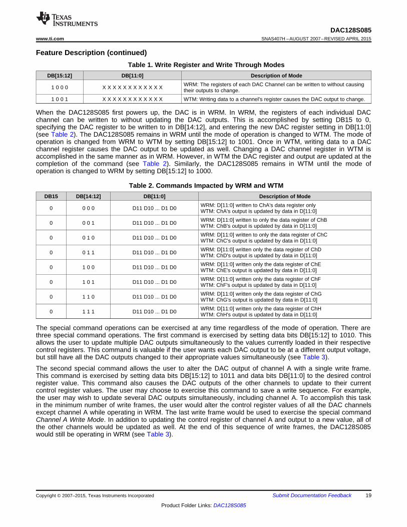
Typical Application (continued)9.2.3 Application Curve
Figure 33. Typical Performance
10 Power Supply RecommendationsFor best performance, the DAC128S085 power supply should be bypassed with at least a 1-µF and a 0.1-µFcapacitor. The 0.1-µF capacitor must be placed right at the device supply pin. The 1-µF or larger valuedcapacitor can be a tantalum capacitor, while the 0.1-µF capacitor must be a ceramic capacitor with low ESL andlow ESR. If a ceramic capacitor with low ESL and low ESR is used for the 1-µF value and can be placed right atthe supply pin, the 0.1-µF capacitor can be eliminated. Capacitors of this nature typically span the samefrequency spectrum as the 0.1-µF capacitor, and thus eliminate the need for the extra capacitor. The powersupply for the DAC128S085 should only be used for analog circuits.
Avoid the crossover of analog and digital signals. This helps minimize the amount of noise from the transitions ofthe digital signals from coupling onto the sensitive analog signals, such as the reference pins and the DACoutputs.
11 Layout
11.1 Layout GuidelinesFor best accuracy and minimum noise, the printed circuit board containing the DAC128S085 should haveseparate analog and digital areas. The areas are defined by the locations of the analog and digital power planes.Both of these planes should be located in the same board layer. A single ground plane is preferred if digitalreturn current does not flow through the analog ground area. Frequently a single ground plane design will utilizea "fencing" technique to prevent the mixing of analog and digital ground current. Separate ground planes shouldonly be utilized when the fencing technique is inadequate. The separate ground planes must be connected inone place, preferably near the DAC128S085. Ensure that digital signals with fast edge rates do not pass oversplit ground planes. The signals must always have a continuous return path below their traces.
Copyright © 2007–2015, Texas Instruments Incorporated Submit Documentation Feedback 23
Product Folder Links: DAC128S085

SYNC
VOUTEVOUTA
VOUTB
VOUTC
VOUTD
VA
VREF1
SCLK
DOUT
DIN
VOUTF
VOUTG
VOUTH
GND
VREF2
GROUND PLANE
To MCU
N.C.
GND
EN
VREF
VIN
VIA to GROUND PLANE
5-V Supply Rail
To loads
To loads
DA
C1
28
S0
85
LM4
13
2
DAC128S085SNAS407H –AUGUST 2007–REVISED APRIL 2015 www.ti.com
11.2 Layout Example
Figure 34. Layout Example
24 Submit Documentation Feedback Copyright © 2007–2015, Texas Instruments Incorporated
Product Folder Links: DAC128S085

DAC128S085www.ti.com SNAS407H –AUGUST 2007–REVISED APRIL 2015
12 Device and Documentation Support
12.1 Device Support
12.1.1 Specification DefinitionsDIFFERENTIAL NON-LINEARITY (DNL) is the measure of the maximum deviation from the ideal step size of 1
LSB, which is VREF / 4096 = VA / 4096.
DAC-to-DAC CROSSTALK is the glitch impulse transferred to a DAC output in response to a full-scale changein the output of another DAC.
DIGITAL CROSSTALK is the glitch impulse transferred to a DAC output at mid-scale in response to a full-scalechange in the input register of another DAC.
DIGITAL FEEDTHROUGH is a measure of the energy injected into the analog output of the DAC from the digitalinputs when the DAC outputs are not updated. It is measured with a full-scale code change on thedata bus.
FULL-SCALE ERROR is the difference between the actual output voltage with a full scale code (FFFh) loadedinto the DAC and the value of VA x 4095 / 4096.
GAIN ERROR is the deviation from the ideal slope of the transfer function. It can be calculated from Zero andFull-Scale Errors as GE = FSE - ZE, where GE is Gain error, FSE is Full-Scale Error and ZE isZero Error.
GLITCH IMPULSE is the energy injected into the analog output when the input code to the DAC registerchanges. It is specified as the area of the glitch in nanovolt-seconds.
INTEGRAL NON-LINEARITY (INL) is a measure of the deviation of each individual code from a straight linethrough the input to output transfer function. The deviation of any given code from this straight lineis measured from the center of that code value. The end point method is used. INL for this productis specified over a limited range, per the Electrical Tables.
LEAST SIGNIFICANT BIT (LSB) is the bit that has the smallest value or weight of all bits in a word. This valueis
LSB = VREF / 2n
where• VREF is the supply voltage for this product, and n is the DAC resolution in bits, which is 12 for the
DAC128S085. (3)
MAXIMUM LOAD CAPACITANCE is the maximum capacitance that can be driven by the DAC with outputstability maintained.
MONOTONICITY is the condition of being monotonic, where the DAC has an output that never decreases whenthe input code increases.
MOST SIGNIFICANT BIT (MSB) is the bit that has the largest value or weight of all bits in a word. Its value is1/2 of VA.
MULTIPLYING BANDWIDTH is the frequency at which the output amplitude falls 3 dB below the input sinewave on VREF1,2 with the DAC code at full-scale.
NOISE SPECTRAL DENSITY is the internally generated random noise. It is measured by loading the DAC tomid-scale and measuring the noise at the output.
POWER EFFICIENCY is the ratio of the output current to the total supply current. The output current comes fromthe power supply. The difference between the supply and output currents is the power consumedby the device without a load.
SETTLING TIME is the time for the output to settle to within 1/2 LSB of the final value after the input code isupdated.
TOTAL HARMONIC DISTORTION PLUS NOISE (THD+N) is the ratio of the harmonics plus the noise presentat the output of the DACs to the rms level of an ideal sine wave applied to VREF1,2 with the DACcode at mid-scale.
Copyright © 2007–2015, Texas Instruments Incorporated Submit Documentation Feedback 25
Product Folder Links: DAC128S085

DAC128S085SNAS407H –AUGUST 2007–REVISED APRIL 2015 www.ti.com
Device Support (continued)WAKE-UP TIME is the time for the output to exit power-down mode. This is the time from the rising edge of
SYNC to when the output voltage deviates from the power-down voltage of 0 V.
ZERO CODE ERROR is the output error, or voltage, present at the DAC output after a code of 000h has beenentered.
12.2 Documentation Support
12.2.1 Related Documentation• LM4132 SOT-23 Precision Low Dropout Voltage Reference, SNVS372
12.3 TrademarksSPI is a trademark of Motorola, Inc..All other trademarks are the property of their respective owners.
12.4 Electrostatic Discharge CautionThese devices have limited built-in ESD protection. The leads should be shorted together or the device placed in conductive foamduring storage or handling to prevent electrostatic damage to the MOS gates.
12.5 GlossarySLYZ022 — TI Glossary.
This glossary lists and explains terms, acronyms, and definitions.
13 Mechanical, Packaging, and Orderable InformationThe following pages include mechanical, packaging, and orderable information. This information is the mostcurrent data available for the designated devices. This data is subject to change without notice and revision ofthis document. For browser-based versions of this data sheet, refer to the left-hand navigation.
26 Submit Documentation Feedback Copyright © 2007–2015, Texas Instruments Incorporated
Product Folder Links: DAC128S085
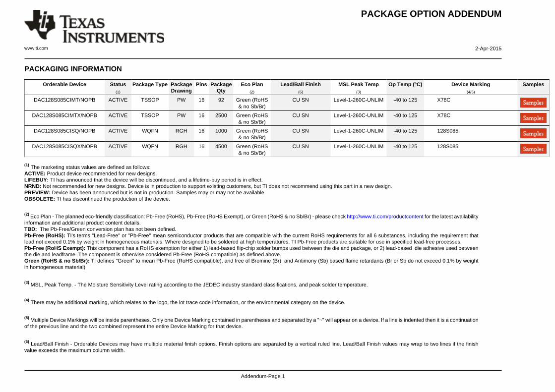
PACKAGE OPTION ADDENDUM
www.ti.com 2-Apr-2015
Addendum-Page 1
PACKAGING INFORMATION
Orderable Device Status(1)
Package Type PackageDrawing
Pins PackageQty
Eco Plan(2)
Lead/Ball Finish(6)
MSL Peak Temp(3)
Op Temp (°C) Device Marking(4/5)
Samples
DAC128S085CIMT/NOPB ACTIVE TSSOP PW 16 92 Green (RoHS& no Sb/Br)
CU SN Level-1-260C-UNLIM -40 to 125 X78C
DAC128S085CIMTX/NOPB ACTIVE TSSOP PW 16 2500 Green (RoHS& no Sb/Br)
CU SN Level-1-260C-UNLIM -40 to 125 X78C
DAC128S085CISQ/NOPB ACTIVE WQFN RGH 16 1000 Green (RoHS& no Sb/Br)
CU SN Level-1-260C-UNLIM -40 to 125 128S085
DAC128S085CISQX/NOPB ACTIVE WQFN RGH 16 4500 Green (RoHS& no Sb/Br)
CU SN Level-1-260C-UNLIM -40 to 125 128S085
(1) The marketing status values are defined as follows:ACTIVE: Product device recommended for new designs.LIFEBUY: TI has announced that the device will be discontinued, and a lifetime-buy period is in effect.NRND: Not recommended for new designs. Device is in production to support existing customers, but TI does not recommend using this part in a new design.PREVIEW: Device has been announced but is not in production. Samples may or may not be available.OBSOLETE: TI has discontinued the production of the device.
(2) Eco Plan - The planned eco-friendly classification: Pb-Free (RoHS), Pb-Free (RoHS Exempt), or Green (RoHS & no Sb/Br) - please check http://www.ti.com/productcontent for the latest availabilityinformation and additional product content details.TBD: The Pb-Free/Green conversion plan has not been defined.Pb-Free (RoHS): TI's terms "Lead-Free" or "Pb-Free" mean semiconductor products that are compatible with the current RoHS requirements for all 6 substances, including the requirement thatlead not exceed 0.1% by weight in homogeneous materials. Where designed to be soldered at high temperatures, TI Pb-Free products are suitable for use in specified lead-free processes.Pb-Free (RoHS Exempt): This component has a RoHS exemption for either 1) lead-based flip-chip solder bumps used between the die and package, or 2) lead-based die adhesive used betweenthe die and leadframe. The component is otherwise considered Pb-Free (RoHS compatible) as defined above.Green (RoHS & no Sb/Br): TI defines "Green" to mean Pb-Free (RoHS compatible), and free of Bromine (Br) and Antimony (Sb) based flame retardants (Br or Sb do not exceed 0.1% by weightin homogeneous material)
(3) MSL, Peak Temp. - The Moisture Sensitivity Level rating according to the JEDEC industry standard classifications, and peak solder temperature.
(4) There may be additional marking, which relates to the logo, the lot trace code information, or the environmental category on the device.
(5) Multiple Device Markings will be inside parentheses. Only one Device Marking contained in parentheses and separated by a "~" will appear on a device. If a line is indented then it is a continuationof the previous line and the two combined represent the entire Device Marking for that device.
(6) Lead/Ball Finish - Orderable Devices may have multiple material finish options. Finish options are separated by a vertical ruled line. Lead/Ball Finish values may wrap to two lines if the finishvalue exceeds the maximum column width.

PACKAGE OPTION ADDENDUM
www.ti.com 2-Apr-2015
Addendum-Page 2
Important Information and Disclaimer:The information provided on this page represents TI's knowledge and belief as of the date that it is provided. TI bases its knowledge and belief on informationprovided by third parties, and makes no representation or warranty as to the accuracy of such information. Efforts are underway to better integrate information from third parties. TI has taken andcontinues to take reasonable steps to provide representative and accurate information but may not have conducted destructive testing or chemical analysis on incoming materials and chemicals.TI and TI suppliers consider certain information to be proprietary, and thus CAS numbers and other limited information may not be available for release.
In no event shall TI's liability arising out of such information exceed the total purchase price of the TI part(s) at issue in this document sold by TI to Customer on an annual basis.

TAPE AND REEL INFORMATION
*All dimensions are nominal
Device PackageType
PackageDrawing
Pins SPQ ReelDiameter
(mm)
ReelWidth
W1 (mm)
A0(mm)
B0(mm)
K0(mm)
P1(mm)
W(mm)
Pin1Quadrant
DAC128S085CISQ/NOPB WQFN RGH 16 1000 178.0 12.4 4.3 4.3 1.3 8.0 12.0 Q1
DAC128S085CISQX/NOPB
WQFN RGH 16 4500 330.0 12.4 4.3 4.3 1.3 8.0 12.0 Q1
PACKAGE MATERIALS INFORMATION
www.ti.com 30-Apr-2018
Pack Materials-Page 1

*All dimensions are nominal
Device Package Type Package Drawing Pins SPQ Length (mm) Width (mm) Height (mm)
DAC128S085CISQ/NOPB WQFN RGH 16 1000 210.0 185.0 35.0
DAC128S085CISQX/NOPB
WQFN RGH 16 4500 367.0 367.0 35.0
PACKAGE MATERIALS INFORMATION
www.ti.com 30-Apr-2018
Pack Materials-Page 2

www.ti.com
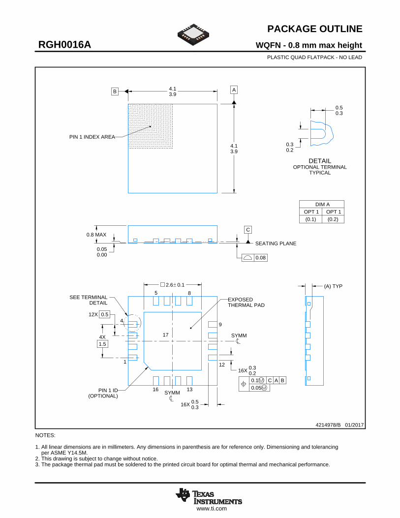
PACKAGE OUTLINE
C
SEE TERMINALDETAIL
16X 0.30.2
2.6 0.1
16X 0.50.3
0.8 MAX
(A) TYP
0.050.00
12X 0.5
4X1.5
B 4.13.9
A
4.13.9
0.30.2
0.50.3
WQFN - 0.8 mm max heightRGH0016APLASTIC QUAD FLATPACK - NO LEAD
4214978/B 01/2017
DIM A OPT 1 OPT 1(0.1) (0.2)
PIN 1 INDEX AREA
0.08
SEATING PLANE
1
49
12
5 8
16 13(OPTIONAL)
PIN 1 ID
0.1 C A B0.05
EXPOSEDTHERMAL PAD
17 SYMM
SYMM
NOTES: 1. All linear dimensions are in millimeters. Any dimensions in parenthesis are for reference only. Dimensioning and tolerancing per ASME Y14.5M. 2. This drawing is subject to change without notice. 3. The package thermal pad must be soldered to the printed circuit board for optimal thermal and mechanical performance.
SCALE 3.000
DETAILOPTIONAL TERMINAL
TYPICAL
www.ti.com
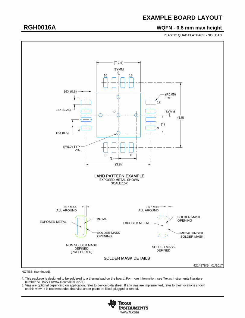
EXAMPLE BOARD LAYOUT
0.07 MINALL AROUND
0.07 MAXALL AROUND
16X (0.25)
16X (0.6)
( 0.2) TYPVIA
12X (0.5)
(3.8)
(3.8)
(1)
( 2.6)
(R0.05)TYP
(1)
WQFN - 0.8 mm max heightRGH0016APLASTIC QUAD FLATPACK - NO LEAD
4214978/B 01/2017
SYMM
1
4
5 8
9
12
1316
SYMM
LAND PATTERN EXAMPLEEXPOSED METAL SHOWN
SCALE:15X
17
NOTES: (continued) 4. This package is designed to be soldered to a thermal pad on the board. For more information, see Texas Instruments literature number SLUA271 (www.ti.com/lit/slua271).5. Vias are optional depending on application, refer to device data sheet. If any vias are implemented, refer to their locations shown on this view. It is recommended that vias under paste be filled, plugged or tented.
SOLDER MASKOPENING
METAL UNDERSOLDER MASK
SOLDER MASKDEFINED
EXPOSED METALMETAL
SOLDER MASKOPENING
SOLDER MASK DETAILS
NON SOLDER MASKDEFINED
(PREFERRED)
EXPOSED METAL
www.ti.com
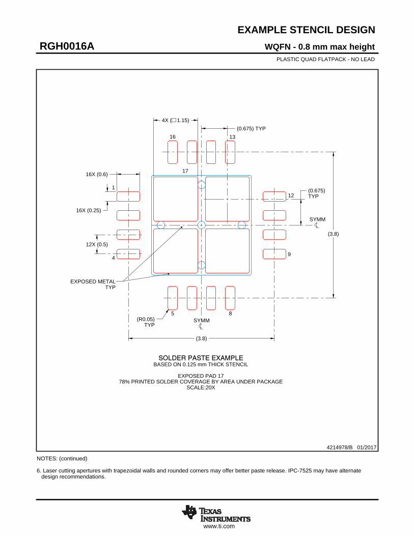
EXAMPLE STENCIL DESIGN
16X (0.6)
16X (0.25)
12X (0.5)
(3.8)
(3.8)
4X ( 1.15)
(0.675)TYP
(0.675) TYP
(R0.05)TYP
WQFN - 0.8 mm max heightRGH0016APLASTIC QUAD FLATPACK - NO LEAD
4214978/B 01/2017
NOTES: (continued) 6. Laser cutting apertures with trapezoidal walls and rounded corners may offer better paste release. IPC-7525 may have alternate design recommendations.
SYMM
TYPEXPOSED METAL
SOLDER PASTE EXAMPLEBASED ON 0.125 mm THICK STENCIL
EXPOSED PAD 17
78% PRINTED SOLDER COVERAGE BY AREA UNDER PACKAGESCALE:20X
SYMM
1
4
5 8
9
12
1316
17
IMPORTANT NOTICE
Texas Instruments Incorporated (TI) reserves the right to make corrections, enhancements, improvements and other changes to itssemiconductor products and services per JESD46, latest issue, and to discontinue any product or service per JESD48, latest issue. Buyersshould obtain the latest relevant information before placing orders and should verify that such information is current and complete.TI’s published terms of sale for semiconductor products (http://www.ti.com/sc/docs/stdterms.htm) apply to the sale of packaged integratedcircuit products that TI has qualified and released to market. Additional terms may apply to the use or sale of other types of TI products andservices.Reproduction of significant portions of TI information in TI data sheets is permissible only if reproduction is without alteration and isaccompanied by all associated warranties, conditions, limitations, and notices. TI is not responsible or liable for such reproduceddocumentation. Information of third parties may be subject to additional restrictions. Resale of TI products or services with statementsdifferent from or beyond the parameters stated by TI for that product or service voids all express and any implied warranties for theassociated TI product or service and is an unfair and deceptive business practice. TI is not responsible or liable for any such statements.Buyers and others who are developing systems that incorporate TI products (collectively, “Designers”) understand and agree that Designersremain responsible for using their independent analysis, evaluation and judgment in designing their applications and that Designers havefull and exclusive responsibility to assure the safety of Designers' applications and compliance of their applications (and of all TI productsused in or for Designers’ applications) with all applicable regulations, laws and other applicable requirements. Designer represents that, withrespect to their applications, Designer has all the necessary expertise to create and implement safeguards that (1) anticipate dangerousconsequences of failures, (2) monitor failures and their consequences, and (3) lessen the likelihood of failures that might cause harm andtake appropriate actions. Designer agrees that prior to using or distributing any applications that include TI products, Designer willthoroughly test such applications and the functionality of such TI products as used in such applications.TI’s provision of technical, application or other design advice, quality characterization, reliability data or other services or information,including, but not limited to, reference designs and materials relating to evaluation modules, (collectively, “TI Resources”) are intended toassist designers who are developing applications that incorporate TI products; by downloading, accessing or using TI Resources in anyway, Designer (individually or, if Designer is acting on behalf of a company, Designer’s company) agrees to use any particular TI Resourcesolely for this purpose and subject to the terms of this Notice.TI’s provision of TI Resources does not expand or otherwise alter TI’s applicable published warranties or warranty disclaimers for TIproducts, and no additional obligations or liabilities arise from TI providing such TI Resources. TI reserves the right to make corrections,enhancements, improvements and other changes to its TI Resources. TI has not conducted any testing other than that specificallydescribed in the published documentation for a particular TI Resource.Designer is authorized to use, copy and modify any individual TI Resource only in connection with the development of applications thatinclude the TI product(s) identified in such TI Resource. NO OTHER LICENSE, EXPRESS OR IMPLIED, BY ESTOPPEL OR OTHERWISETO ANY OTHER TI INTELLECTUAL PROPERTY RIGHT, AND NO LICENSE TO ANY TECHNOLOGY OR INTELLECTUAL PROPERTYRIGHT OF TI OR ANY THIRD PARTY IS GRANTED HEREIN, including but not limited to any patent right, copyright, mask work right, orother intellectual property right relating to any combination, machine, or process in which TI products or services are used. Informationregarding or referencing third-party products or services does not constitute a license to use such products or services, or a warranty orendorsement thereof. Use of TI Resources may require a license from a third party under the patents or other intellectual property of thethird party, or a license from TI under the patents or other intellectual property of TI.TI RESOURCES ARE PROVIDED “AS IS” AND WITH ALL FAULTS. TI DISCLAIMS ALL OTHER WARRANTIES ORREPRESENTATIONS, EXPRESS OR IMPLIED, REGARDING RESOURCES OR USE THEREOF, INCLUDING BUT NOT LIMITED TOACCURACY OR COMPLETENESS, TITLE, ANY EPIDEMIC FAILURE WARRANTY AND ANY IMPLIED WARRANTIES OFMERCHANTABILITY, FITNESS FOR A PARTICULAR PURPOSE, AND NON-INFRINGEMENT OF ANY THIRD PARTY INTELLECTUALPROPERTY RIGHTS. TI SHALL NOT BE LIABLE FOR AND SHALL NOT DEFEND OR INDEMNIFY DESIGNER AGAINST ANY CLAIM,INCLUDING BUT NOT LIMITED TO ANY INFRINGEMENT CLAIM THAT RELATES TO OR IS BASED ON ANY COMBINATION OFPRODUCTS EVEN IF DESCRIBED IN TI RESOURCES OR OTHERWISE. IN NO EVENT SHALL TI BE LIABLE FOR ANY ACTUAL,DIRECT, SPECIAL, COLLATERAL, INDIRECT, PUNITIVE, INCIDENTAL, CONSEQUENTIAL OR EXEMPLARY DAMAGES INCONNECTION WITH OR ARISING OUT OF TI RESOURCES OR USE THEREOF, AND REGARDLESS OF WHETHER TI HAS BEENADVISED OF THE POSSIBILITY OF SUCH DAMAGES.Unless TI has explicitly designated an individual product as meeting the requirements of a particular industry standard (e.g., ISO/TS 16949and ISO 26262), TI is not responsible for any failure to meet such industry standard requirements.Where TI specifically promotes products as facilitating functional safety or as compliant with industry functional safety standards, suchproducts are intended to help enable customers to design and create their own applications that meet applicable functional safety standardsand requirements. Using products in an application does not by itself establish any safety features in the application. Designers mustensure compliance with safety-related requirements and standards applicable to their applications. Designer may not use any TI products inlife-critical medical equipment unless authorized officers of the parties have executed a special contract specifically governing such use.Life-critical medical equipment is medical equipment where failure of such equipment would cause serious bodily injury or death (e.g., lifesupport, pacemakers, defibrillators, heart pumps, neurostimulators, and implantables). Such equipment includes, without limitation, allmedical devices identified by the U.S. Food and Drug Administration as Class III devices and equivalent classifications outside the U.S.TI may expressly designate certain products as completing a particular qualification (e.g., Q100, Military Grade, or Enhanced Product).Designers agree that it has the necessary expertise to select the product with the appropriate qualification designation for their applicationsand that proper product selection is at Designers’ own risk. Designers are solely responsible for compliance with all legal and regulatoryrequirements in connection with such selection.Designer will fully indemnify TI and its representatives against any damages, costs, losses, and/or liabilities arising out of Designer’s non-compliance with the terms and provisions of this Notice.
Mailing Address: Texas Instruments, Post Office Box 655303, Dallas, Texas 75265Copyright © 2018, Texas Instruments Incorporated