perovskites: transforming photovoltaics, a mini … transforming photovoltaics, a mini-review ......
TRANSCRIPT

Perovskites: transformingphotovoltaics, a mini-review
Ashwith Kumar ChilveryAshok K. BatraBin YangKai XiaoPadmaja GuggillaMohan D. AggarwalRaja SurabhiRavi B. LalJames R. CurrieBenjamin G. Penn
Downloaded From: https://www.spiedigitallibrary.org/journals/Journal-of-Photonics-for-Energy on 6/8/2018 Terms of Use: https://www.spiedigitallibrary.org/terms-of-use

Perovskites: transforming photovoltaics, a mini-review
Ashwith Kumar Chilvery,a,b,* Ashok K. Batra,b Bin Yang,c Kai Xiao,c
Padmaja Guggilla,b Mohan D. Aggarwal,b Raja Surabhi,b Ravi B. Lal,b
James R. Currie,d and Benjamin G. Pennd
aTalladega College, Department of Physics, 627 West Battle Street, Talladega, Alabama 35610,United States
bAlabama A&M University, Material Science Group, Department of Physics, Chemistry andMathematics, 4900 Meridian Street, Normal, Alabama 35762, United States
cCenter for Nanophase Material Science, Oak Ridge National Laboratory, Bethel Valley Road,Oak Ridge, Tennessee 37831, United States
dNASA-Marshall Space Flight Center, Sensors Group, Redstone Arsenal, Huntsville, Albama35811, United States
Abstract. The recent power-packed advent of perovskite solar cells is transforming photovol-taics (PV) with their superior efficiencies, ease of fabrication, and cost. This perovskite solar cellfurther boasts of many unexplored features that can further enhance its PV properties and lead toit being branded as a successful commercial product. This article provides a detailed insight ofthe organometal halide based perovskite structure, its unique stoichiometric design, and itsunderlying principles for PV applications. The compatibility of various PV layers and its fab-rication methods is also discussed. © 2015 Society of Photo-Optical Instrumentation Engineers (SPIE)[DOI: 10.1117/1.JPE.5.057402]
Keywords: perovskites; charge transport; dielectric; photovoltaics; efficiency.
Paper 14060SS received Sep. 12, 2014; accepted for publication Nov. 14, 2014; published onlineJan. 6, 2015.
1 Introduction
Solar energy, an infinite producer of photons with a broad range of wavelengths, continues to bea potential source of clean energy. The photovoltaic (PV) process is considered as an idealenergy conversion process that can meet this requirement.1 The International EnergyAgency’s technology roadmap estimates that by 2050, PV will provide ∼11% of all global elec-tricity production and avoid 2.3 gigatonnes of CO2 emissions per year.2 Given these predictions,photovoltaics or light-to-voltage converting devices have gained unprecedented attention fromthe research communities in the previous decades. Many researchers believe that solar cells, thebasic building block of photovoltaics, are on the verge of creating a big impact by providingsustainable and efficient energy via cost-effective methods.
The Sun’s energy can be harnessed in many ways. One example could be of a PVmodule thatconverts solar energy into electricity and a solar thermal collector that converts solar energy intoheat, such as for domestic hot water or room heating.3 Hence, exploring ways to realize PV ascheaper, reliable, and durable ways to generate power is of interest to the scientific community.Silicon, the 14th element on the periodic table, is crucial for PV material in today’s world.However, there is still a need for newer materials and methodologies that offer better throughputsand efficiencies.4
The first generation of the solar cells dates back to 1953, when Gerald Pearson, DarylChapin, and Calvin Fuller discovered the silicon solar cell at AT&T Bell Labs.5 Currently,they trail on the efficiency chart at 25%.6 The use of polycrystalline silicon, thin films, and
*Address all correspondence to: Ashwith Kumar Chilvery, E-mail: [email protected]
This review manuscript is also part of the section on “Breakthroughs in Photonics and Energy,” highlighting primarily recent advances inthe last three years.
0091-3286/2015/$25.00 © 2015 SPIE
REVIEW
Journal of Photonics for Energy 057402-1 Vol. 5, 2015
Downloaded From: https://www.spiedigitallibrary.org/journals/Journal-of-Photonics-for-Energy on 6/8/2018 Terms of Use: https://www.spiedigitallibrary.org/terms-of-use

compound semiconductors rose in the era of second-generation solar cells, which entered the PVmarket in 1981.7 Currently, second-generation solar cells top the efficiency chart at 45%.8 Inearly 2000, organic solar cells paved way for a third wave of PV technology, which bringsthe advantages of flexibility, cost-effectiveness, and ease of fabrication. Though silicon-based solar cells continue to dominate over thin-film technologies and are flying high dueto impressive efficiencies and better lifetimes, it is still in the interest of mankind to unwrapthe organic horizon of solar cells. Therefore, there has been a greater demand in the past decadeon scientists to discover flexible, cheaper, mass producible, and lightweight organic solar cells.One possible alternative to address this problem is to develop PV cells from materials that can beprocessed as easily as plastics. Augmenting this demand, the conferring of the Nobel Prize inChemistry for the year 2000 to Dr. Alan Heeger in recognition of his work on conducting poly-mers has decisively paved a new era in the field of organic electronics, organic photovoltaics(OPVs), and organic/flexible displays.9 This has, in turn, led to the flexible third-generation solarcells, which are organic, dye-sensitized, and polymer. Figure 1 briefly differentiates inorganicsolar cells from their organic counterparts.
Organic solar cells (OSC) or plastic solar cells are an evolving multidisciplinary area ofresearch that involve theoretical, experimental, and design challenges dealing with carbon-based materials and other organic compounds.10 It is a brand of polymer solar cell that incor-porates a conductive organic polymer for light absorption, exciton dissociation, and charge trans-port to generate electricity.11 The OPVs based on a single conducting polymer can achieveefficiencies >7%12 and are still showing potential to increase this. They are different fromthe conventional silicon and other inorganic material based cells as they are cheaper and canbe fabricated via low-cost solution processing techniques, such as spin coating, brush painting,and spray coating.4 These solution-processing techniques yield desired thicknesses of a few hun-dred nanometers and sober efficiencies of 4 to 5%. The wide multipolymer layered architecturesof OSCs help execute the processes of photon trapping, generation of electrons and holes, andtransport of charges to the respective cathodes and anodes. It was later reported that an effectiveway to improve polymer solar cell efficiency is to use a tandem structure; with this method, abroader part of the spectrum of solar radiation is used and the thermalization loss of photonenergy is minimized. Yang Yang reported power conversion efficiencies of >10% in tandemsolar cells.13 Recently, Heliatek and Mitsubishi Chemicals have claimed the highest efficiencyof 12 (Ref. 14) and 10%,15 respectively, for OSCs. Another kind of device is dye-sensitized solarcells (DSSCs), which have gained unparalleled growth in recent years due to their ease of fab-rication and superior tunable optical properties. Recently, a DSSC with porphyrin sensitizers hasachieved a record efficiency of 13% without sacrificing stability.16
The key drawbacks, such as efficiency, durability, and stability of OSCs and DSSCs, havemade them the least chosen products for commercialization. In 2009, perovskites, a new solar
Fig. 1 Basic classification of photovoltaics.
Chilvery et al.: Perovskites: transforming photovoltaics, a mini-review
Journal of Photonics for Energy 057402-2 Vol. 5, 2015
Downloaded From: https://www.spiedigitallibrary.org/journals/Journal-of-Photonics-for-Energy on 6/8/2018 Terms of Use: https://www.spiedigitallibrary.org/terms-of-use

cell material, evolved to transform photovoltaics and currently displays outstanding potentialwith power conversion efficiencies of 19.7%17 in the laboratory. Perovskite-based solar cellsare purported to have the potential to provide sustainable and efficient power via cost-effectivemodes and techniques. Several research groups, such as Henry Snaith from Oxford University,Andrew Rappe at University of Pennsylvania, Sang II Seok at South Korean Institute KRICT,Michael Gratzel from EPFL, and Yang Yang from UCLA, are the frontrunners in the efforts todouble the efficiency of these materials in less than a year.18–21 These devices are at the point ofmaximum optimism and are predicted to reach 50% efficiencies in the near future.22 These devi-ces are also known for their high photon absorptivity, wide direct band gaps with superior carriercharge transports,23 and cost-effective modes of fabrication.
2 Significance of Perovskites
Perovskite is a mineral that came into existence when a German mineralogist, Gustav Rose,discovered calcium titanate (CaTiO3) in 1839; it is named after a Russian mineralogist, LewA. Perovski. Additionally, the compounds having a similar nomenclature to CaTiO3 or the fam-ily of materials exhibiting the stoichiometry as ABX3 are also known as perovskites. This ambi-guity of terminology of the structural family and a mineral has been explicitly elucidated byMuller and Roy.24 They sought to address the ambiguity by proposing that the original mineralcomposition would be enclosed in square brackets. Thus, [CaTiO3] stands for the perovskitestructures and not the composition CaTiO3.
The A, B, and X in the perovskite crystal structure are typically represented as a larger rareearth metal cation, a smaller metal cation, and anions (O2−, Cl−, Br−, I−, or, in a few instances,S2−), respectively, arranged in octahedral symmetry as shown in Fig. 2. In the idealized (cubic)perovskite structure, the large A cations are in 12 coordinates and the smaller B cations occupyoctahedral holes formed by the large X anions. There are many different perovskite materials,such as CaTiO3, MgSiO3, SrFeO3, BaTiO3, LiNbO3, SrZrO3, and the nonoxide KMgF3, that,with skilled chemical manipulation, can produce an incredibly wide array of phases with a multi-tude of functionalities that include dielectric,25,26 ferroelectric,27–30 magnetoresistive,28 thermo-electric,31 electro-optic,32 semiconducting,33 conducting,28,34 and superconduction.29,35
The concept of a two-dimensional layered organic-inorganic perovskite structure was derivedfrom the three-dimensional (3-D) ABX3 structure by cutting 3-D perovskite into one layer thickslice along the h100i direction.36 It is known from the first-principles study that the replacementof an inorganic A cation in a basic cubic perovskite structure by a suitable organic cation pro-vides a material of a superior scope with a broad selection of properties.37 In the early 1990s, anIBM researcher, David B. Mitzi, explored the structure-property relationship in organic-inor-ganic hybrid perovskite materials by replacing A with a cationic organic molecule, B withan inorganic post-transition metal, and X with halides, such as methylammonium tin iodide
Fig. 2 (a) Typical octahedral structure of pervoskite crystal (ABX3). (b) Detailed features of per-ovskite solar devices.
Chilvery et al.: Perovskites: transforming photovoltaics, a mini-review
Journal of Photonics for Energy 057402-3 Vol. 5, 2015
Downloaded From: https://www.spiedigitallibrary.org/journals/Journal-of-Photonics-for-Energy on 6/8/2018 Terms of Use: https://www.spiedigitallibrary.org/terms-of-use
(CH3NH3SnI3) and methyl ammonium lead iodide (CH3NH3PbI3).29 These organo-metal hal-
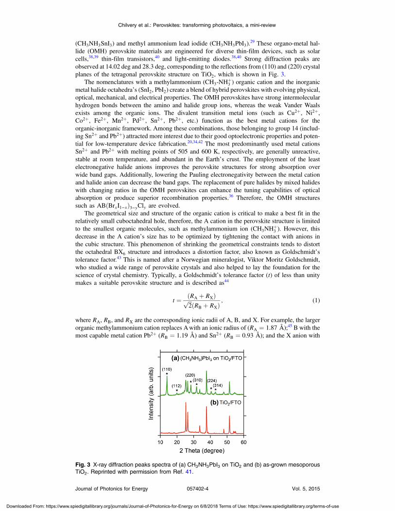
lide (OMH) perovskite materials are engineered for diverse thin-film devices, such as solarcells,38,39 thin-film transistors,40 and light-emitting diodes.38,40 Strong diffraction peaks areobserved at 14.02 deg and 28.3 deg, corresponding to the reflections from (110) and (220) crystalplanes of the tetragonal perovskite structure on TiO2, which is shown in Fig. 3.
The nomenclatures with a methylammonium (CH3-NHþ3 ) organic cation and the inorganic
metal halide octahedra’s (SnI2, PbI2) create a blend of hybrid perovskites with evolving physical,optical, mechanical, and electrical properties. The OMH perovskites have strong intermolecularhydrogen bonds between the amino and halide group ions, whereas the weak Vander Waalsexists among the organic ions. The divalent transition metal ions (such as Cu2þ, Ni2þ,Co2þ, Fe2þ, Mn2þ, Pd2þ, Sn2þ, Pb2þ, etc.) function as the best metal cations for theorganic-inorganic framework. Among these combinations, those belonging to group 14 (includ-ing Sn2þ and Pb2þ) attracted more interest due to their good optoelectronic properties and poten-tial for low-temperature device fabrication.20,34,42 The most predominantly used metal cationsSn2þ and Pb2þ with melting points of 505 and 600 K, respectively, are generally unreactive,stable at room temperature, and abundant in the Earth’s crust. The employment of the leastelectronegative halide anions improves the perovskite structures for strong absorption overwide band gaps. Additionally, lowering the Pauling electronegativity between the metal cationand halide anion can decrease the band gaps. The replacement of pure halides by mixed halideswith changing ratios in the OMH perovskites can enhance the tuning capabilities of opticalabsorption or produce superior recombination properties.36 Therefore, the OMH structuressuch as ABðBrxI1−xÞ3−yCly are evolved.
The geometrical size and structure of the organic cation is critical to make a best fit in therelatively small cuboctahedral hole, therefore, the A cation in the perovskite structure is limitedto the smallest organic molecules, such as methylammonium ion (CH3NH
þ3 ). However, this
decrease in the A cation’s size has to be optimized by tightening the contact with anions inthe cubic structure. This phenomenon of shrinking the geometrical constraints tends to distortthe octahedral BX6 structure and introduces a distortion factor, also known as Goldschmidt’stolerance factor.43 This is named after a Norwegian mineralogist, Viktor Moritz Goldschmidt,who studied a wide range of perovskite crystals and also helped to lay the foundation for thescience of crystal chemistry. Typically, a Goldschmidt’s tolerance factor (t) of less than unitymakes a suitable perovskite structure and is described as44
t ¼ ðRA þ RXÞffiffiffi
2p ðRB þ RXÞ
; (1)
where RA, RB, and RX are the corresponding ionic radii of A, B, and X. For example, the largerorganic methylammonium cation replaces Awith an ionic radius of (RA ¼ 1.87 Å);45 B with themost capable metal cation Pb2þ (RB ¼ 1.19 Å) and Sn2þ (RB ¼ 0.93 Å); and the X anion with
Fig. 3 X-ray diffraction peaks spectra of (a) CH3NH3PbI3 on TiO2 and (b) as-grown mesoporousTiO2. Reprinted with permission from Ref. 41.
Chilvery et al.: Perovskites: transforming photovoltaics, a mini-review
Journal of Photonics for Energy 057402-4 Vol. 5, 2015
Downloaded From: https://www.spiedigitallibrary.org/journals/Journal-of-Photonics-for-Energy on 6/8/2018 Terms of Use: https://www.spiedigitallibrary.org/terms-of-use

the uniquely distinguished halide ions Cl− (RX ¼ 1.81 Å), Br− (RX ¼ 1.96 Å), and I−
(RX ¼ 2.2 Å). It is evident from the above geometries that the lead halide perovskites(0.84 < t < 0.86) have higher tolerations than their tin (0.91 < t < 0.95) counterparts;hence, the superior properties of lead over tin perovskites is demonstrated and the use oflead is justified.
3 Atomistic Origin and Charge Transport Mechanism in OMHPerovskites
In the diverse field of solar cells, the selection of materials of merit is critical and, in some cases,is presented as a trade-off factor among durability, stability, cost, ease of fabrication, and effi-ciency. An ideal solar cell material requires inheriting properties such as stronger and broaderabsorptions, ultrafast carrier charges separation and transport, high dielectric, and optimizeddiffusion lengths so that swift recombination occurs. By extending its organic and inorganicfeatures to the bottlenecked efficiencies of organic PVs, the 3-D framework of methylammoniummetal halide perovskite becomes an important modern scientific breakthrough. Typical absorp-tion spectra of perovskite devices and its normalized spectra as a function of TiO2 thickness areshown in Fig. 4.
In 2009, Miyasaka et al. published a report on using OMH perovksites as visible light sen-sitizers yielding efficiencies of 3.81%, where it interacts with the conduction band levels ofTiO2.
39 Further investigations on these class of materials have revealed that they can augmentthe efficiencies and are exceptional to low electron and hole transport lengths, which are pre-dominant among low-temperature solution-processed PV.21,46–48
3.1 Dielectric Behavior
The compelling ferroelectric properties of 3-D structured OMH perovskites can be explained bythe polar nature of methylammonium salt (CH3-NH
þ3 ) with a permanent dipole moment, and the
structural distortions carried by the lone pairs of lead (6s2) and tin (5s2). These cubic superlat-tices consisting of semiconductor metal iodide layers sandwiched between insulator methylam-monium layers can easily change their orientation and, thus, create the octahedral dielectricconfinement of excitons.49 Typically, the excitons in organic molecules observe the Frenkel-Peierls model, leading to stronger bonds between them, higher exciton binding energies, andthe least Bohr radius. These characteristics, consequently, tend to lower the dielectric constantsand contribute to a poor charge transport in the conventional organic PV. On the contrary, theexcitons in OMH perovskites exhibit the Wannier-Mott model30,50 due to their organic and inor-ganic behaviors. In these materials, the excitons experience the least binding energies and higher
Fig. 4 UV-Vis absorption spectra of (a) CH3NH3PbI3 on TiO2 and (b) normalized absoprtion as afunction of TiO2 thickness. Reprinted with permission from Ref. 41.
Chilvery et al.: Perovskites: transforming photovoltaics, a mini-review
Journal of Photonics for Energy 057402-5 Vol. 5, 2015
Downloaded From: https://www.spiedigitallibrary.org/journals/Journal-of-Photonics-for-Energy on 6/8/2018 Terms of Use: https://www.spiedigitallibrary.org/terms-of-use
Bohr’s excitonic radius, thereby yielding superior charge transports. The exciton-evaluatingcomponents can be described by the well-known equations of binding energy (Eb) and theBohr radius (rB) of the excitons,
Eb ¼ 13.6μ
ε2ðeVÞ; (2)
rB ¼ 0.529ε
μðA0Þ; (3)
where ε is the dielectric permittivity and μ is the exciton pair mass. Table 1 presents the trends indielectric constants for various halides. However, the strong inherited polarization due to theionic compounds (which have permanent dipole moment), the presence of an inorganicanion, and an organic cation yields higher dielectric constants, thus exhibiting a smooth mecha-nism for good long-range charge transport via band structure or polaron hopping.35 Table 1details the dielectric and exciton behaviors in OMH perovskites.
3.2 Charge Transport
The charge transport in OMH perovskite solar cells mostly resembles the conventional DSSCs.Zhao and Zhu report that the intensity-modulated photocurrent or photovoltage spectroscopiesshow that the transport and recombination properties of solid-state mesostructured perovskitesolar cells are similar to those of solid-state DSSCs.41 They also report that the electron diffusionlength decreases from 16.9 to 5.5 μm as the TiO2 film thickness increases from 1.8 to 8.3 μm,revealing that the light absorption increases with an increasing TiO2 film thickness, therebyallowing for faster recombination which limits the solar conversion process.
Recently, Wehrenfennig et al. concluded that the OMH perovskites allow for an unexpectedcombination of both low charge recombination rates and high charge-carrier mobilities and are,therefore, the best candidates for light absorption and charge transport in solar cells.56 It is nec-essary to further explore the charge transports and electronic structures of OMH perovskite mate-rials. The relativistic GW (Green’s function and Wick’s theorem of density functional theory)calculations on the electronic and optical properties predictMASnI3 to be a better electron trans-porter thanMAPbI3.
57 It is evident from Fig. 5 that the resistivity versus temperature of lead- andtin-based perovskites is similar to the characteristics of undoped semiconductor and displays aperfect ohmic behavior.33
However, these OMH perovskite materials act as light sensitizers and ambipolar electron andhole transport materials,58 or they absorb light, thus creating the excitons (electron-hole pair).This involves steps like (1) creation of electron-hole pairs upon absorption of light by the per-ovskite; (2) formation of excitons after thermalization of the carriers; (3) charge separations atthe junctions of electron and hole transport layers (HTLs); (4) injection of holes and electronsinto the respective transport layers, such as spiro-2,2’,7,7’-tetrakis-(N,N-di-p-methoxyphenyl-amine)9,9’-spirobifluorene (OMeTAD) and TiO2; (5) extraction of those charge carriers tothe external circuit by contacts. Thus, it is vital to understand the OMH perovskite materialstoichiometry and cell architecture to arrive at the best cell performance. So far, two types
Table 1 Dielectric and optical parameters of organo-metal halide (OMH) perovskites.
OMH Crystal structure ColorDielectricconstant
Opticalband gap
Bohrradius (rB)
Exciton bindingenergy (Eb)
MAPbI3 Cubic (330.4 K)51 Tetragonal(161.4 K) Orthorhombic (161.4 K)
Black 28.8(Ref. 45)
1.63 eV(Ref. 52)
22 Å 37 meV(Ref. 53)
MAPbBr3 Cubic (236.3 K)51 Tetragonal(154 K) Orthorhombic (148.8 K)
Yellowishorange
25.5(Ref. 45)
2.32 eV(Ref. 54)
20 Å 76 meV
MAPbCl3 Cubic (177.2 K)51 Tetragonal(171.4 K) Orthorhombic (171.4 K)
Colorless 23.9(Ref. 45)
3.11 eV(Ref. 55)
17 Å 100 meV
Chilvery et al.: Perovskites: transforming photovoltaics, a mini-review
Journal of Photonics for Energy 057402-6 Vol. 5, 2015
Downloaded From: https://www.spiedigitallibrary.org/journals/Journal-of-Photonics-for-Energy on 6/8/2018 Terms of Use: https://www.spiedigitallibrary.org/terms-of-use

of device architectures, namely mesostructured and planar heterojunction, have been adapted.Figure 6 describes the band structure of a typical perovskite solar cell. The first mesostructure isderived from the conventional solid-state DSSCs, and in the latter, the perovskite layer is sand-wiched between the electron (TiO2, Al2O3, etc.) and hole [poly(3-hexylthiopene-2,5-diyl(P3HT), spiro-OMeTAD, etc.] transport layers. Figure 7(a) displays the typical cross-sectionalSEM image of mesostructured architecture of perovskite solar cells and reveals that the pores ofthe mp-TiO2 film are infiltrated with CH3NH3PbI3 perovskite. The surface SEM image in Fig. 7(b) is crucial for determining the filling fraction and infiltration depth of CH3NH3PbI3 and HTLinto mp-TiO2. The transparent conducting oxide films, such as indium tin oxide (ITO) and fluo-rine-doped tin oxide (FTO), are widely used as electrodes due to their striking features such aslow electrical resistance, high optical transmittance, and high photoconductivity.59 However,ITO and FTO are limited by the infrared wavelengths; in particular, the ITO-based substrateshave low thermal stability, which explains the high efficiencies produced by FTOs.
The mechanism of conduction depends largely on charge-carrier diffusion length, which gen-erally means a thicker absorber layer for greater light trapping and is considered one of the keyparameters of solar cell performance. After photoexcitation, the electron-hole pairs generated aredissociated in a few picoseconds (∼2 ps). The presence of metal oxide TiO2 with a high electronaffinity accelerates the formation of charges and motivates efficient electron injection for <1 ps.The faster electron injection in CH3NH3PbI3∕TiO2 is supported by the terahertz (THz) photo-conductivity transient kinetic studies with normalized excitation density, which shows that thecharge mobility of CH3NH3PbI3∕TiO2 (∼7.5 cm2∕V · s) is three to four times lower than that inneat CH3NH3PbI3 and CH3NH3PbI3∕Al2O3 (∼20 cm2∕V · s).61 However, the unbalanced trans-port of charges resulting in space charge limited photocurrents and a lowering of the power
Fig. 5 The temperature-dependent resistivity plots of lead- and tin-based perovskite single crys-tals. Reprinted with permission from Ref. 33.
Fig. 6 Energy band levels of TiO2∕CH3NH3PbI3∕spiro-OMeTAD showing the conduction andvalence bands. Reprinted with permission from Ref. 48.
Chilvery et al.: Perovskites: transforming photovoltaics, a mini-review
Journal of Photonics for Energy 057402-7 Vol. 5, 2015
Downloaded From: https://www.spiedigitallibrary.org/journals/Journal-of-Photonics-for-Energy on 6/8/2018 Terms of Use: https://www.spiedigitallibrary.org/terms-of-use

conversion efficiency (PCE) can be attributed to the low intrinsic mobility of TiO2.62 A few other
research groups have reported higher efficiencies of 15.7% with Al2O3 layers63 and 4.2% with
ZrO2 buffer layer,58 respectively.The THz photoconductivity spectra of pristine OMH perovskite shown in Fig. 8 compares its
composition with TiO2 and Al2O3. Slow electron–hole recombination and persistent high mobil-ity are essential features for an efficient solar cell. The THz response along with other methodsconcluded that the THz mobilities of electrons are twice as mobile as the holes in the perovskitephase.61
The degradation of OMH perovskites with humidity, ambient light, and oxidation can beattributed to the strong absorption onset of the material shifting from 1.6 to 2.4 eV. Thislow Urbach energy measured for perovskites can be a strong indicator that this material willnot suffer from the Staebler–Wronski effect.64 The degradation of the cell performance is nor-mally accompanied by a color bleaching of perovskites even when the cells are stored in thedark, suggesting that the chemical instability of perovskites in the iodide electrolyte contributesto the degradation of the cell performance over time. The exact degradation mechanism is stillunknown, and it is crucial to know to what extent the material changes when measured at anambient atmosphere or when exposed to liquid electrolytes. Therefore, a number of detaileddegradation studies are required to further explore its usage for photoelectrochemical applica-tions in the future.
The OMH perovskite layer, typically with thicknesses of ∼100 to 200 nm, determines theexciton diffusion lengths (Ld) and their lifetimes (τ), unlike the OSCs with a larger Ld than these(CH3NH3PbI3) materials (5 to 10 nm), and yields extended exciton lifetimes of>50 ns (Ref. 65)
Fig. 7 (a) Cross-sectional SEM image of organo-metal halide (OMH) perovskite. (b) Surface SEMimage of CH3NH3PbI3 on TiO2. Reprinted with permission from Ref. 60.
Fig. 8 Terahertz photoconductivity spectra of TiO2∕CH3NH3PbI3 and Al2O3∕CH3NH3PbI3 at dif-ferent pump probe delays. Reprinted with permission from Ref. 61.
Chilvery et al.: Perovskites: transforming photovoltaics, a mini-review
Journal of Photonics for Energy 057402-8 Vol. 5, 2015
Downloaded From: https://www.spiedigitallibrary.org/journals/Journal-of-Photonics-for-Energy on 6/8/2018 Terms of Use: https://www.spiedigitallibrary.org/terms-of-use

when compared to 8 ns of OSC,66 motivating them to travel to the contacts before decay. Variousresearch groups have investigated different halides (Cl, Br, and I),51,67,68 and mixed halides, suchas CH3NH3PbI2Cl, CH3NH3PbI2Br, or vice versa.
38,50,63,69 However, the destructive effects oflead (Pb) brands tin (Sn) as a more suitable potential candidate for the perovskite structure. Mitziinvestigated its (CH3NH3SnI3) applicability for tuning the band gap, which was later introducedby various others31,33,34,36,38 as a key feature of conducting photovoltaics. A maximum PCE of12.3% was achieved with CH3NH3PbI2Br. It is evident from Table 1 that the optical band gapsand exciton binding energies follow a trend, indicating the tunability and application-specificfunctionalities. However, a detailed study in different mixed halide materials is required to deter-mine the electronic and optical properties.
Typically, the perovskite solar cells suffer from high series and shunt resistance, therebyyielding poor fill factor values. This can be attributed to the higher conductivity of the perovskitelayer being surpassed by the thicker layer of the lower conductive hole transport material (HTM)layer. Therefore, a thinner and better conductive HTM layer that enhances the hole mobility ishighly desired for these devices. Bi et al. reported PCEs of 8.5, 4.5, and 1.6% by incorporatingvarious HTMs, such as spiro-OMeTAD, P3HT, and 4-(diethylamino)-benzaldehyde diphenyl-hydrazone, respectively.70 Eventually, spiro-OMeTAD caught the attention of researchers and itwas discovered that doping a lithium salt lithilum bis-trifluoromethanesulfonimide (Li-TFSI)can increase hole conductivity.71 The spectroscopy studies later revealed that the Fermi levelin spiro-OMeTAD shifts toward the HOMO, and 24% of the spiro-OMeTAD molecules getoxidized in presence of Li-TFSI.72 Spiro-OMeTAD as a superior HTM layer is widely usedto improve the device performance through enhancing its conductivity, as they mainly func-tioned to increase the hole mobility and charge density of HTMs, respectively, or increaseboth simultaneously.73 Figure 9 shows the J–V curves for various perovskite devices withmixed and pure compositions.
4 Fabrication Procedures
The fabrication methodologies technically drive the performance and efficiency of perovskitesolar cells, so it is vital to deposit the light sensitizer OMH perovskite material to enhance thedevice kinetics. The thinner cells tend to poorly absorb light, whereas in thicker cells, the chargecarriers cannot travel through to reach the contacts.74 Despite their higher performance, theydegrade at a faster rate, which is normally accompanied by a color bleaching due to the chemicalinstability of perovskites in the iodide electrolyte.41 Figure 10(a) showcases a multitude of
Fig. 9 J–V curves of various OMH perovskite devices: (a) TiO2∕CH3NH3PbI3∕spiro-OMeTAD,(b) TiO2∕CH3NH3PbI3∕spiro-OMeTAD, (c) TiO2∕CH3NH3PbI3−XClX∕spiro-OMeTAD, (d) gra-phene-TiO2∕meso-Al2O3∕CH3NH3PbI3−XClX∕spiro-OMeTAD, (e) ZnO∕CH3NH3PbI3∕spiro-OMeTAD, (f) TiO2∕CH3NH3PbI3−XClX∕spiro-OMeTAD. Reproduced with permission fromRef. 20.
Chilvery et al.: Perovskites: transforming photovoltaics, a mini-review
Journal of Photonics for Energy 057402-9 Vol. 5, 2015
Downloaded From: https://www.spiedigitallibrary.org/journals/Journal-of-Photonics-for-Energy on 6/8/2018 Terms of Use: https://www.spiedigitallibrary.org/terms-of-use
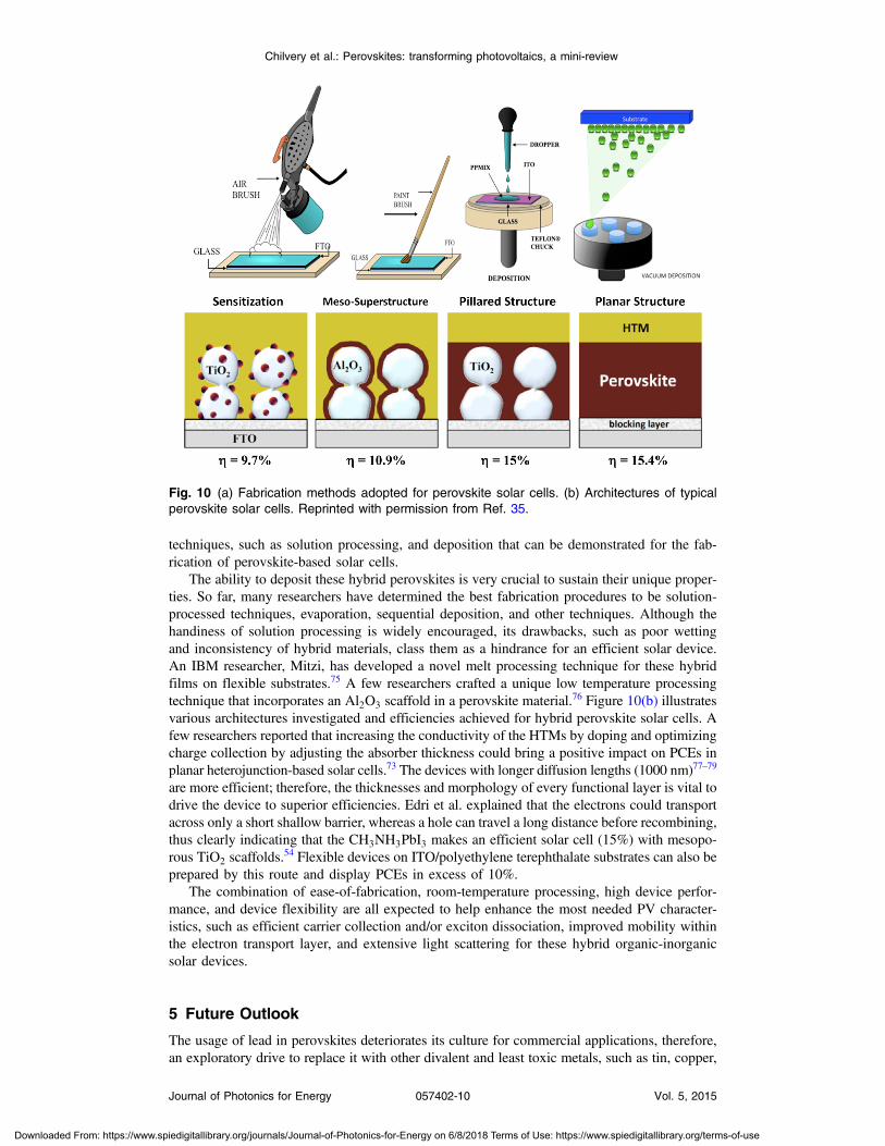
techniques, such as solution processing, and deposition that can be demonstrated for the fab-rication of perovskite-based solar cells.
The ability to deposit these hybrid perovskites is very crucial to sustain their unique proper-ties. So far, many researchers have determined the best fabrication procedures to be solution-processed techniques, evaporation, sequential deposition, and other techniques. Although thehandiness of solution processing is widely encouraged, its drawbacks, such as poor wettingand inconsistency of hybrid materials, class them as a hindrance for an efficient solar device.An IBM researcher, Mitzi, has developed a novel melt processing technique for these hybridfilms on flexible substrates.75 A few researchers crafted a unique low temperature processingtechnique that incorporates an Al2O3 scaffold in a perovskite material.76 Figure 10(b) illustratesvarious architectures investigated and efficiencies achieved for hybrid perovskite solar cells. Afew researchers reported that increasing the conductivity of the HTMs by doping and optimizingcharge collection by adjusting the absorber thickness could bring a positive impact on PCEs inplanar heterojunction-based solar cells.73 The devices with longer diffusion lengths (1000 nm)77–79
are more efficient; therefore, the thicknesses and morphology of every functional layer is vital todrive the device to superior efficiencies. Edri et al. explained that the electrons could transportacross only a short shallow barrier, whereas a hole can travel a long distance before recombining,thus clearly indicating that the CH3NH3PbI3 makes an efficient solar cell (15%) with mesopo-rous TiO2 scaffolds.
54 Flexible devices on ITO/polyethylene terephthalate substrates can also beprepared by this route and display PCEs in excess of 10%.
The combination of ease-of-fabrication, room-temperature processing, high device perfor-mance, and device flexibility are all expected to help enhance the most needed PV character-istics, such as efficient carrier collection and/or exciton dissociation, improved mobility withinthe electron transport layer, and extensive light scattering for these hybrid organic-inorganicsolar devices.
5 Future Outlook
The usage of lead in perovskites deteriorates its culture for commercial applications, therefore,an exploratory drive to replace it with other divalent and least toxic metals, such as tin, copper,
Fig. 10 (a) Fabrication methods adopted for perovskite solar cells. (b) Architectures of typicalperovskite solar cells. Reprinted with permission from Ref. 35.
Chilvery et al.: Perovskites: transforming photovoltaics, a mini-review
Journal of Photonics for Energy 057402-10 Vol. 5, 2015
Downloaded From: https://www.spiedigitallibrary.org/journals/Journal-of-Photonics-for-Energy on 6/8/2018 Terms of Use: https://www.spiedigitallibrary.org/terms-of-use

germanium, manganese, or iron, can change the dynamics of perovskite solar cells; currentresearch is trending along these lines. The scientific community anticipates that these particulardevices will make a successful entry to the commercial market by 2020. Further, exploration ofsuperior materials that can tune ferroelectric domains and provide rapid support to the excitonicreactions in perovskite crystals can yield a better class of devices with the best durability anddegradability.
The recent advent of nanotechnology makes it worthwhile to investigate the role of nano-perovskites to enrich the performance and efficiency of any device. Additionally, the device costcan revolutionize the current photovoltaic technology, which is possible by developing morebench-top processes, such as printing, spraying, etc., rather than the clean room and high-tech equipment. Hence, there is a great need and urgency to develop an easy methodologyof fabricating these devices. Some researchers believe that it can resemble the single crystalsilicon and an OMH perovskite single crystal grown by melt-process or gel method will beeventually be a reality. Finally, its high transparency (>825 nm) is a predictor of superior func-tionalities by integrating these exotic devices in a tandem architecture.
Acknowledgments
The authors acknowledge the DHS-BS and NSF-EPSCoR program and summer research pro-gram facilitated by Oak Ridge National Laboratory’s HBCU/MEI program.
References
1. S. Kazim et al., “Perovskite as light harvester: a game changer in photovoltaics,” Angew.Chem. Int. Ed. Engl. 53(11), 2812–2824 (2014).
2. P. Frankl, “Technology roadmap: solar photovoltaic energy,” 11 May 2010, http://www.iea.org/publications/freepublications/publication/technology-roadmap-solar-photovoltaic-energy---foldout.html (18 November 2014).
3. S. A. Kalogirou, “Solar thermal collectors and applications,” Prog. Energy Combust. Sci.30(3), 231–295 (2004).
4. A. K. Chilvery et al., “A versatile technique for the fabrication of PEDOT: PSS films fororganic solar cells,” Energy, Sci. Technol. 4(2), 6–11 (2012).
5. S.-S. Sun and N. S. Sariciftci, Organic Photovoltaics, p. 640, CRC Press, T&F Group,London (2005).
6. NREL Cell Efficiencies, “efficiency_chart” (2012).7. M. A. Green, “Crystalline and thin-film silicon solar cells: state of the art and future poten-
tial,” Sol. Energy 74(3), 181–192 (2003).8. M. A. Green et al., “Solar cell efficiency tables,” Prog. Photovolt. Res. Appl. 20, 12–20
(2012).9. H. Shirakawa et al., “Synthesis of electrically conducting organic polymers: halogen deriv-
atives of polyacetylene, (CH) x,” J. Chem. Soc. Chem. Commun. 16, 578 (1977).10. M. Pagliaro, R. Ciriminna, and G. Palmisano, “Flexible solar cells,” ChemSusChem 1(11),
880–891 (2008).11. A. C. Mayer et al., “Polymer-based solar cells,” Mater. Today 10(11), 28–33 (2007).12. G. Li, R. Zhu, and Y. Yang, “Polymer solar cells,” Nat. Photonics 6, 153–161 (2012).13. J. You et al., “A polymer tandem solar cell with 10.6% power conversion efficiency,” Nat.
Commun. 4, 1446 (2013).14. Heliatek, “Heliatek press release,” 2013, http://www.heliatek.com/?lang=en (18 November
2014).15. M. C. Scharber and N. S. Sariciftci, “Efficiency of bulk-heterojunction organic solar cells,”
Prog. Polym. Sci. 38(12), 1929–1940 (2013).16. P. Simon et al., “Dye-sensitized solar cells with 13% efficiency achieved through the
molecular engineering of porphyrin sensitizers,” Nat. Chem. 6, 242–247 (2014).17. H. Zhou et al., “Interface engineering of highly efficient perovskite solar cells,” Science
345(6196), 542–546 (2014).
Chilvery et al.: Perovskites: transforming photovoltaics, a mini-review
Journal of Photonics for Energy 057402-11 Vol. 5, 2015
Downloaded From: https://www.spiedigitallibrary.org/journals/Journal-of-Photonics-for-Energy on 6/8/2018 Terms of Use: https://www.spiedigitallibrary.org/terms-of-use

18. M. Liu, M. B. Johnston, and H. J. Snaith, “Efficient planar heterojunction perovskite solarcells by vapour deposition,” Nature 501(7467), 395–398 (2013).
19. I. Grinberg et al., “Perovskite oxides for visible-light-absorbing ferroelectric and photovol-taic materials,” Nature 503(7477), 509–517 (2013).
20. P. Gao, M. Grätzel, and M. K. Nazeeruddin, “Organohalide lead perovskites for photovol-taic applications,” Energy Environ. Sci. 7(8), 2448–2463 (2014).
21. J. You et al., “Perovskite solar cells with high efficiency and flexibility,” ACS Nano 8(2),1674–1680 (2014).
22. B. Bulkin, “Perovskites: the future of solar power?,” in Guardian, p. 1, http://www.theguardian.com/sustainable-business/perovskites-future-solar-power (18 November 2014).
23. H. J. Snaith, “Perovskites: the emergence of a new era for low-cost, high-efficiency solarcells,” J. Phys. Chem. Lett. 4, 3623–3630 (2013).
24. O. Muller and R. Roy, “The major ternary structural families,” in Cryst. Chem. Non-MetallicMater., Springer-Verlag, Berlin, Heidelbergle (1974).
25. E. J. Juarez-Perez et al., “Photoinduced giant dielectric constant in lead halide perovskitesolar cells,” J. Phys. Chem. Lett. 5(13), 2390–2394 (2014).
26. A. K. Batra et al., “Simulation of energy harvesting from roads via pyroelectricity,”J. Photonics Energy 1(1), 014001 (2011).
27. A. A. Bokov and Z. G. Ye, “Recent progress in relaxor ferroelectrics with perovskite struc-ture,” J. Mater. Sci. 41(1), 31–52 (2006).
28. M. A. Loi and J. C. Hummelen, “Hybrid solar cells: perovskites under the Sun,” Nat. Mater.12(12), 1087–1089 (2013).
29. D. B. Mitzi, “Synthesis, structure, and properties of organic-inorganic perovskites andrelated materials,” in Progress in Inorganic Chemistry, K. D. Karlin, Ed., p. 121, JohnWiley & Sons, West Sussex, England, New York (1999).
30. J. M. Frost et al., “Atomistic origins of high-performance in hybrid halide perovskite solarcells,” Nano Lett. 14(5), 2584–2590 (2014).
31. Y. Takahashi et al., “Charge transport in tin-iodide perovskite: origin of high conductivity,”Dalt. Trans. 40(20), 5563–5568 (2011).
32. A. Bhalla, R. Guo, and R. Roy, “The perovskite structure—a review of its role in ceramicscience and technology,” Mater. Res. Innov. 4(1), 3–26 (2000).
33. C. C. Stoumpos, C. D. Malliakas, and M. G. Kanatzidis, “Semiconducting tin and leadiodide perovskites with organic cations: phase transitions, high mobilities, and near-infraredphotoluminescent properties,” Inorg. Chem. 52(15), 9019–9038 (2013).
34. D. B. Mitzi et al., “Conducting tin halides with a layered organic-based perovskite struc-ture,” Nature 369, 467–469 (1994).
35. H.-S. Kim, S. H. Im, and N.-G. Park, “Organolead halide perovskite: new horizons in solarcell research,” J. Phys. Chem. C 118(11), 5615–5625 (2014).
36. J. L. Knutson, J. D. Martin, and D. B. Mitzi, “Tuning the band gap in hybrid tin iodideperovskite semiconductors using structural templating,” Inorg. Chem. 44(13), 4699–4705 (2005).
37. R. S. Roth, “Classification of perovskite and other AB03 type compounds,” J. Res. Natl.Bur. Stand. (1934). 58(2), 75–88 (1957).
38. D. B. Mitzi, “Templating and structural engineering in organic-inorganic perovskites,”J. Chem. Soc. Dalt. Trans. 1(1), 1–12 (2001).
39. A. Kojima et al., “Organometal halide perovskites as visible-light sensitizers for photovol-taic cells,” J. Am. Chem. Soc. 131(17), 6050–6051 (2009).
40. D. B. Mitzi, K. Chondroudis, and C. R. Kagan, “Organic-inorganic electronics,” IBM J. Res.Dev. 45(1), 29–45 (2001).
41. Y. Zhao and K. Zhu, “Charge transport and recombination in perovskite (CH3NH3) PbI3sensitized TiO2 solar cells,” J. Phys. Chem. Lett. 4, 2880–2884 (2013).
42. I. B. Koutselas, L. Ducasse, and G. C. Papavassiliou, “Electronic properties of three- andlow-dimensional semiconducting materials with Pb halide and Sn halide units,” J. Phys.Condens. Matter 8, 1217–1227 (1996).
43. X. W. Zhou, F. P. Doty, and P. Yang, “Atomistic models for scintillatory discovery,” Proc.SPIE 7806, 78060E (2010).
Chilvery et al.: Perovskites: transforming photovoltaics, a mini-review
Journal of Photonics for Energy 057402-12 Vol. 5, 2015
Downloaded From: https://www.spiedigitallibrary.org/journals/Journal-of-Photonics-for-Energy on 6/8/2018 Terms of Use: https://www.spiedigitallibrary.org/terms-of-use

44. V. M. Goldschmidt, “Geochemisce Verterlungsgesetze der Elemente,” in Nor. Videnskap,Oslo, I kommission hos J. Dybwad, Oslo (1927).
45. A. Poglitsch and D. Weber, “Dynamic disorder in methylammoniumtrihalogenoplumbates(II) observed by millimeter-wave spectroscopy,” J. Chem. Phys. 87(11), 6373 (1987).
46. G. Xing et al., “Long-range balanced electron- and hole-transport lengths in organic-inor-ganic CH3NH3PbI3,” Science 342(6156), 344–347 (2013).
47. H. J. Snaith, “Estimating the maximum attainable efficiency in dye-sensitized solar cells,”Adv. Funct. Mater. 20(1), 13–19 (2010).
48. N. Park, “Organometal perovskite light absorbers toward a 20% efficiency low-cost solid-state mesoscopic solar cell,” J. Phys. Chem. Lett. 4, 2423–2429 (2013).
49. N. A. Gippius et al., “Dielectrically confined excitons and polaritons in natural superlattices—perovskite lead iodide semiconductors,” J. Phys. IV 3, 437–440 (1993).
50. S. a. Bretschneider et al., “Research update: physical and electrical characteristics of leadhalide perovskites for solar cell applications,” APL Mater. 2(4), 040701 (2014).
51. H. Mashiyama and Y. Kurihara, “Disordered cubic perovskite structure of CH3NH3PbX3
(X ¼ Cl, Br, I),” J. Korean Phys. Soc. 32, 156–158 (1998).52. Z. Chen et al., “Shape-controlled synthesis of organolead halide perovskite nanocrystals and
their tunable optical absorption,” Mater. Res. Express 1(1), 015034 (2014).53. B. Conings et al., “Perovskite-based hybrid solar cells exceeding 10% efficiency with high
reproducibility using a thin film sandwich approach,” Adv. Mater. 26(13), 2041–2046(2014).
54. E. Edri et al., “High open-circuit voltage solar cells based on organic-inorganic lead bro-mide perovskite,” J. Phys. Chem. Lett. 4(6), 897–902 (2013).
55. N. Kitazawa, Y. Watanabe, and Y. Nakamura, “Optical properties of CH3NH3PbX3
(X ¼ halogen) and their mixed-halide crystals,” J. Mater. Sci. 37, 3585–3587 (2002).56. C. Wehrenfennig et al., “High charge carrier mobilities and lifetimes in organolead trihalide
perovskites,” Adv. Mater. 26(10), 1584–1589 (2014).57. P. Umari, E. Mosconi, and F. De Angelis, “Relativistic GW calculations on CH3NH3PbI3
and CH3NH3SnI3 perovskites for solar cell applications,” Sci. Rep. 4, 4467 (2014).58. H.-S. Kim et al., “Mechanism of carrier accumulation in perovskite thin-absorber solar
cells,” Nat. Commun. 4, 2242 (2013).59. D.-J. Kwak et al., “Comparison of transparent conductive indium tin oxide, titanium-doped
indium oxide, and fluorine-doped tin oxide films for dye-sensitized solar cell application,”J. Electr. Eng. Technol. 6(5), 684–687 (2011).
60. J. H. Heo et al., “Efficient inorganic-organic hybrid heterojunction solar cells containingperovskite compound and polymeric hole conductors,” Nat. Photonics 7(June), 486–491(2013).
61. C. S. Ponseca et al., “Organometal halide perovskite solar cell materials rationalized: ultra-fast charge generation, high and microsecond-long balanced mobilities, and slow recombi-nation,” J. Am. Chem. Soc. 136(14), 5189–5192 (2014).
62. E. Hendry et al., “Local field effects on electron transport in nanostructured TiO2 revealedby terahertz spectroscopy,” Nano Lett. 6, 755–759 (2006).
63. M. M. Lee et al., “Efficient hybrid solar cells based on meso-superstructured organometalhalide perovskites,” Science 338(6107), 643–647 (2012).
64. S. De Wolf et al., “Organometallic halide perovskites: sharp optical absorption edgeand its relation to photovoltaic performance,” J. Phys. Chem. Lett. 5(6), 1035–1039(2014).
65. H.-S. Kim et al., “Lead iodide perovskite sensitized all-solid-state submicron thin filmmesoscopic solar cell with efficiency exceeding 9%,” Sci. Rep. 2, 591 (2012).
66. R. L. Headrick et al., “Anisotropic mobility in large grain size solution processed organicsemiconductor thin films,” Appl. Phys. Lett. 92(6), 063302 (2008).
67. B. Suarez et al., “Recombination study of combined halides (Cl, Br, I) perovskite solarcells,” J. Phys. Chem. Lett. 5(10), 1628–1635 (2014).
68. M. Meister, “Charge generation and recombination in hybrid organic / inorganic solar cells,”p. 250, PhD Thesis, Johannes Gutenberg-University Mainz (2013).
Chilvery et al.: Perovskites: transforming photovoltaics, a mini-review
Journal of Photonics for Energy 057402-13 Vol. 5, 2015
Downloaded From: https://www.spiedigitallibrary.org/journals/Journal-of-Photonics-for-Energy on 6/8/2018 Terms of Use: https://www.spiedigitallibrary.org/terms-of-use

69. K. Liang, D. B. Mitzi, and M. T. Prikas, “Synthesis and characterization of organic—inor-ganic perovskite thin films prepared using a versatile two-step dipping technique,” Chem.Mater. 10(1), 403–411 (1998).
70. D. Bi et al., “Using a two-step deposition technique to prepare perovskite (CH3NH3PbI3)for thin film solar cells based on ZrO2 and TiO2 mesostructures,” RSC Adv. 3, 18762–18766(2013).
71. H. Snaith and M. Gratzel, “Enhanced charge mobility in a molecular hole transporter viaaddition of redox inactive ionic dopant: implication to dye-sensitized solar cells,” Appl.Phys. Lett. 89, 262114 (2006).
72. R. Scholin et al., “Energy level shifts in spiro-OMeTAD molecular thin films when addingLi-TFSI,” J. Phys. Chem. 116, 26300–26305 (2012).
73. F. Liu et al., “Numerical simulation: toward the design of high-efficiency planar perovskitesolar cells,” Appl. Phys. Lett. 104(25), 253508 (2014).
74. G. Xing et al., “Long-range balanced electron- and hole-transport lengths in organic-inor-ganic CH3NH3PbI3,” Science 342(6156), 344–347 (2013).
75. D. B. Mitzi, D. R. Medeiros, and P. W. Dehaven, “Low-temperature melt processing oforganic-inorganic hybrid films,” Chem. Mater. 14(7), 2839–2841 (2002).
76. M. Carnie et al., “A one-step low temperature processing route for organolead halide per-ovskite solar cells,” Chem. Commun. 49, 7893–7895 (2013).
77. Y. Zhao, A. M. Nardes, and K. Zhu, “Solid-state mesostructured perovskite CH3NH3PbI3solar cells: charge transport, recombination, and diffusion length,” J. Phys. Chem. Lett. 5,490–494 (2014).
78. V. Gonzalez-Pedro et al., “General working principles of CH3NH3PbX3 perovskite solarcells,” Nano Lett. 14(2), 888–893 (2014).
79. L. Barnea-nehoshtan et al., “Surface photovoltage spectroscopy study of organo-lead per-ovskite solar cells,” Phys. Chem. Lett. 5, 2408–2413 (2014).
Biographies of the authors are not available.
Chilvery et al.: Perovskites: transforming photovoltaics, a mini-review
Journal of Photonics for Energy 057402-14 Vol. 5, 2015
Downloaded From: https://www.spiedigitallibrary.org/journals/Journal-of-Photonics-for-Energy on 6/8/2018 Terms of Use: https://www.spiedigitallibrary.org/terms-of-use