partiiilectures multistage amplifiers · in multistage amplifier, where it is used as a final...
TRANSCRIPT

University of Missan Multistage Amplifiers
Electrical Engineering Department
Second Year, Electronic II,2015-2016 Maab Alaa Hussain
1
University of missan
Electrical Engineering Department
Electronic II, Second year
2015-2016
PartIIILectures
Multistage Amplifiers
Assistant Lecture: Maab Alaa Hussain
University of Missan Multistage Amplifiers
Electrical Engineering Department
Second Year, Electronic II,2015-2016 Maab Alaa Hussain
2
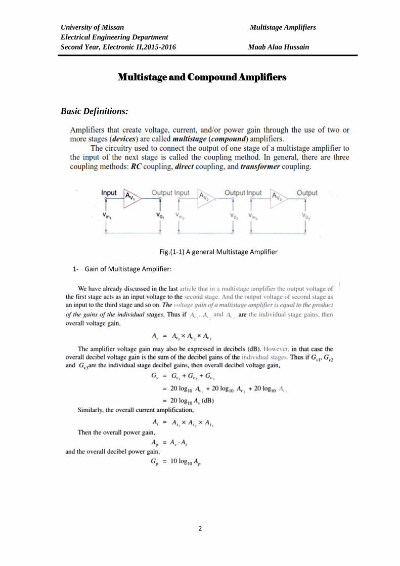
Multistage and Compound Amplifiers
Basic Definitions:
Fig.(1-1) A general Multistage Amplifier
1- Gain of Multistage Amplifier:

University of Missan Multistage Amplifiers
Electrical Engineering Department
Second Year, Electronic II,2015-2016 Maab Alaa Hussain
3
Example: A given amplifier arrangement has the following voltage gains.
Av1=10, Av2=20 and Av3=40. What is the overall gain? Also express each
gain in dB and determine the total dB voltage gain.
Solution:
Example: Three amplifier stages are working in cascade with 0.05v peak
to peak input providing 150v peak-to-peak output. If the voltage gain of
the first stage is 20and input to the third stage is 15v peak-to-peak.
Determine:
i. The overall voltage gain.
ii. Voltage gain of 2nd
and 3rd
stages.
iii. Input voltage of the 2nd
stage.
Solution:

University of Missan Multistage Amplifiers
Electrical Engineering Department
Second Year, Electronic II,2015-2016 Maab Alaa Hussain
4

University of Missan Multistage Amplifiers
Electrical Engineering Department
Second Year, Electronic II,2015-2016 Maab Alaa Hussain
5
2- Different Coupling schemes Used in Amplifiers:
1- Resistance –Capacitance (RC) coupling:
It is the most important method of coupling the signal from one stage to
the next stage and is shown in Fig.(1-2)a. in this method the signal
developed across the collector resistor of each stage is coupled through
capacitor into the base of the next stage. The cascaded stages amplify the
signal and overall gain is equal to the product of individual stage gains.
The amplifier using this coupling scheme, are called RC-coupled
amplifiers.
Fig.(2-1)
University of Missan Multistage Amplifiers
Electrical Engineering Department
Second Year, Electronic II,2015-2016 Maab Alaa Hussain
6
2. Impedance coupling:
This coupling is shown in Fig.(1-2)b. it may be noted that the Rc is
replaced by an inductor (L). as frequency increases the XL(equal to W.L)
increases. In other word inductor pass direct current but block alternating
current. The amplifier using this scheme, are called impedance-coupling
amplifiers.
3. Transformer Coupling:
This coupling is shown in fig.(1-2)c. in this method, primary winding
of the transistor acts as a collector load and secondary winding conveys
the a.c. output signal directly to the base of the next stage. The amplifiers
using this scheme of coupling are called transformer coupled amplifiers.
4. Direct Coupling:
This is shown in Fig.(1-2)d. in this method the a.c. output signal is fed
directly to the next stage. This type is used low frequency signales to be
amplified.

University of Missan Multistage Amplifiers
Electrical Engineering Department
Second Year, Electronic II,2015-2016 Maab Alaa Hussain
7
1- RC coupled amplifier:
Fig.(1-3)

University of Missan Multistage Amplifiers
Electrical Engineering Department
Second Year, Electronic II,2015-2016 Maab Alaa Hussain
8
1-1 calculation of Voltage Gain for RC Coupled Amplifies:
Fig.(1-4)
The parameters re1' and re2' represent the a.c. emitter diode transmittance
of Q1 and Q2 respectively.
Re1'=26/IE1 and re2
'=26/IE2
Now the Ri of the first stage as in fig.(1-4)a
Ri2=RB // (1.re1')=1.re1' (if RB>> 1re1')
Ro=Rc//Ri2
Where: Ri2 the input of the 2nd
stage.
Ri1=RB//(2.re2') =2.re2' (if RB>>2.re2')
Ro2=Rc//RL

University of Missan Multistage Amplifiers
Electrical Engineering Department
Second Year, Electronic II,2015-2016 Maab Alaa Hussain
9
AV1=1.1
1
i
o
R
R=1.
'
1
1
'
11
1
. e
o
o
o
r
R
r
R
Av2= '
2
2
e
o
r
R
Av=Av1.Av2= '
2
2
'
1
1 .e
o
e
o
r
R
r
R
If Q1 and Q2 are identical , then re1'=re2'=re'
And :
Av=Av1.Av2= 2'
21.
e
oo
r
RR
Example: Determine Ri, Ro, Ai, Av, for the first stage and second stage
for the circuit shown in Fig.(1-5). Also determine the overall voltage gain
and the gain in dB.
Solution:
Given Vcc=10v, Rc=5kΩ, RB=1MΩ, RE=1kΩ, RL=10kΩ, 1=2=100.
Fig.(1-5)
Ri for first and second stages:

University of Missan Multistage Amplifiers
Electrical Engineering Department
Second Year, Electronic II,2015-2016 Maab Alaa Hussain
10
The input resistance for the first stage:
The input resistance for the second stage:
The output resistance for the first and second stages:
H.W: A radio receiver uses a two stage RC coupled amplifier
shown in the figure below, determine the values of voltage gain
of each stage and overall voltage gain.

University of Missan Multistage Amplifiers
Electrical Engineering Department
Second Year, Electronic II,2015-2016 Maab Alaa Hussain
11
1-2 Advantages and Disadvantages of RC Coupled Amplifier
a. Advantages:
It is the most convenient and least expensive multistage amplifier.
It has wide frequency response.
It provides less frequency distortion.
b. Disadvantages:
The overall gain of amplifier is comparatively small because of the
loading effect of successive stages.
It has tendency to become noisy with age, especially in moist
climates.
It provides poor resistance matching between stages.
1-3 Application of RC Coupled Amplifiers
The RC coupled amplifier has excellent frequency response from 50
HZ to 20KHZ. This property makes it very useful in the initial stages of
all the public address systems. However, it may be noted that a coupled
amplifier cannot be used as a final stage of that amplifier because of its
poor matching characteristics.

University of Missan Multistage Amplifiers
Electrical Engineering Department
Second Year, Electronic II,2015-2016 Maab Alaa Hussain
12
2- Impedance Coupled:
Fig. (1-6)shows the two stage impedance coupled amplifier. The
circuit consists of two single stage C.E amplifiers. The inductor (L) the
capacitor (Cc) and resistor (RB) forms the coupling network. The function
of C1,C2, and CE are the same as explained in RC coupled amplifier.
Fig.(1-6)
The expression of overall voltage gain and individual gains may be
obtained in the same way as obtained for RC coupled amplifier. The only
change to be made is that Rc should be obtained by inductive reactance
(XL=WL). Thus voltage gain of the first stage ,
Av2=Ro2/re2'
Av=Av1.Av2

University of Missan Multistage Amplifiers
Electrical Engineering Department
Second Year, Electronic II,2015-2016 Maab Alaa Hussain
13
3- Transformer coupled Amplifier
Fig.(1-7) shows a two stage transformer coupled amplifier. The circuit
consists of two single stage C.E amplifiers. The function of transformer
(T1) is to couple the a.c. output signal from the output of the first stage to
the input of the second stage, while transformer (T2) couples the output
signal to the load. The input coupling capacitor is C1, while the emitter
bypass capacitor is CE.
Fig.(1-7)
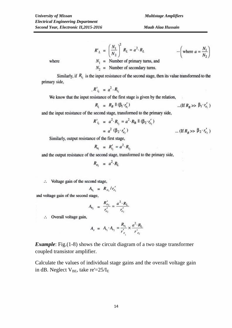
3-1 calculation of Voltages Gain for Transformer coupled Amplifier:
University of Missan Multistage Amplifiers
Electrical Engineering Department
Second Year, Electronic II,2015-2016 Maab Alaa Hussain
14
Example: Fig.(1-8) shows the circuit diagram of a two stage transformer
coupled transistor amplifier.
Calculate the values of individual stage gains and the overall voltage gain
in dB. Neglect VBE, take re'=25/IE

University of Missan Multistage Amplifiers
Electrical Engineering Department
Second Year, Electronic II,2015-2016 Maab Alaa Hussain
15
Fig.(1-8)
Solution:

University of Missan Multistage Amplifiers
Electrical Engineering Department
Second Year, Electronic II,2015-2016 Maab Alaa Hussain
16
3-2 Advantages and Disadvantages of Transformer Coupled Amplifier:
a. Advantages:
No signal power is lost in the collector or base resistors, because of
the low winding resistance of the transformer.
It provides a higher voltage gain than RC coupled amplifier.
It provides an excellent resistance matching between the stages.
b. Disadvantages:
The coupling transformer is expensive and bulky, particularly
when operated at audio frequencies.
At radio frequencies, the winding inductance and distributed
capacitance produce reverse frequency distortion.
It tends to produce 'hum' in the circuit.
University of Missan Multistage Amplifiers
Electrical Engineering Department
Second Year, Electronic II,2015-2016 Maab Alaa Hussain
17
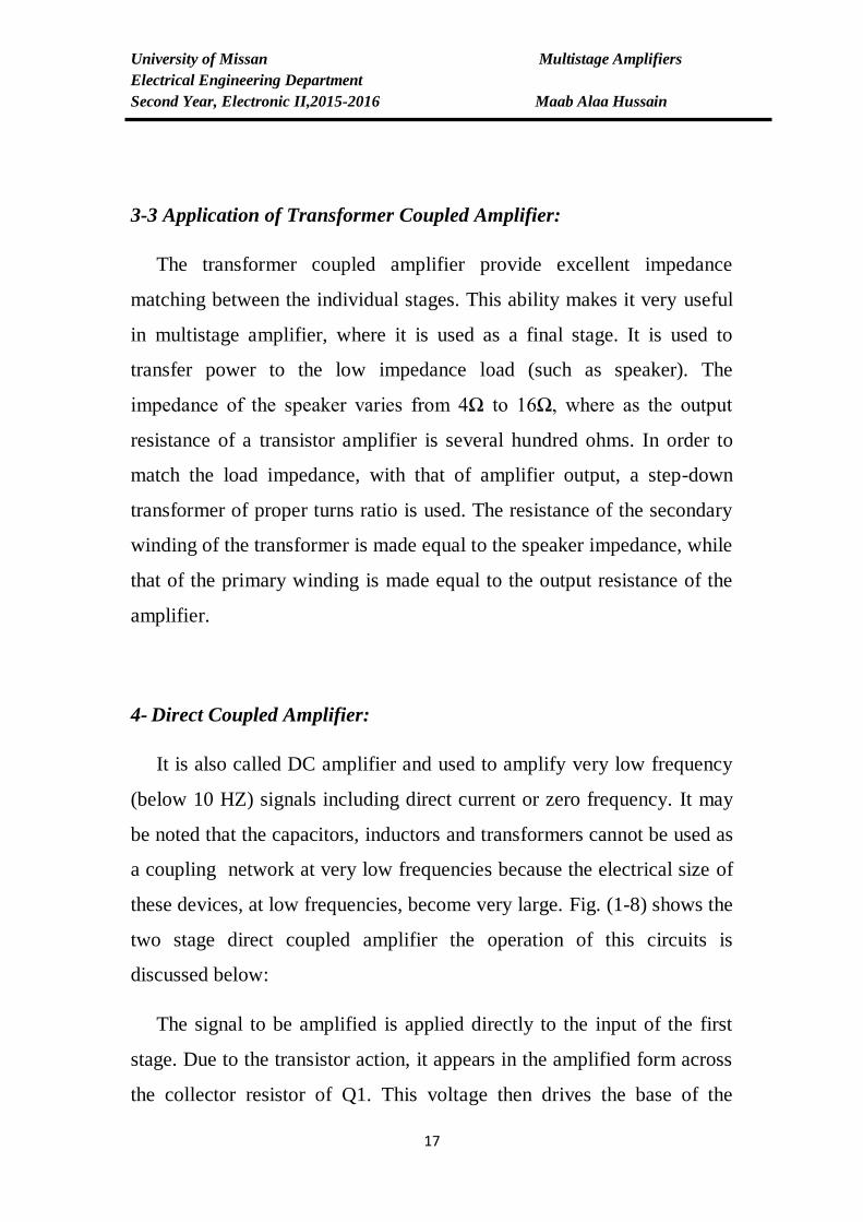
3-3 Application of Transformer Coupled Amplifier:
The transformer coupled amplifier provide excellent impedance
matching between the individual stages. This ability makes it very useful
in multistage amplifier, where it is used as a final stage. It is used to
transfer power to the low impedance load (such as speaker). The
impedance of the speaker varies from 4Ω to 16Ω, where as the output
resistance of a transistor amplifier is several hundred ohms. In order to
match the load impedance, with that of amplifier output, a step-down
transformer of proper turns ratio is used. The resistance of the secondary
winding of the transformer is made equal to the speaker impedance, while
that of the primary winding is made equal to the output resistance of the
amplifier.
4- Direct Coupled Amplifier:
It is also called DC amplifier and used to amplify very low frequency
(below 10 HZ) signals including direct current or zero frequency. It may
be noted that the capacitors, inductors and transformers cannot be used as
a coupling network at very low frequencies because the electrical size of
these devices, at low frequencies, become very large. Fig. (1-8) shows the
two stage direct coupled amplifier the operation of this circuits is
discussed below:
The signal to be amplified is applied directly to the input of the first
stage. Due to the transistor action, it appears in the amplified form across
the collector resistor of Q1. This voltage then drives the base of the

University of Missan Multistage Amplifiers
Electrical Engineering Department
Second Year, Electronic II,2015-2016 Maab Alaa Hussain
18
second transistor Q2 and the amplified output is obtained across the
collector resistor of Q2.
Fig.(1-8)
4-1 calculation of Voltage Gain of Direct Coupled Amplifier:
Consider Fig.(1-9).
Fig.(1-9)

University of Missan Multistage Amplifiers
Electrical Engineering Department
Second Year, Electronic II,2015-2016 Maab Alaa Hussain
19
Example: for the following figure determine the individual stages a.c.
voltage gains and the overall voltage gain. Neglect VBE, take re'=26/IE in
mA, 1=2=100.
Solution:

University of Missan Multistage Amplifiers
Electrical Engineering Department
Second Year, Electronic II,2015-2016 Maab Alaa Hussain
20
Individual stages a.c. voltage gain
The voltage across R2:

University of Missan Multistage Amplifiers
Electrical Engineering Department
Second Year, Electronic II,2015-2016 Maab Alaa Hussain
21
4-2 Direct coupled amplifier using complementary transistor:
Figure (1-10) shows the two stage direct coupled amplifier using
complementary transistors. The term 'complementary' means that one
Fig. (1-10)
stage uses NPN transistor while the second stage uses PNP transistor. The
operation of the circuit may be understood from the condition that when
the positive going input signal is applied to the base of transistor Q1, its
collector current increases. This increases the voltage across R3due to
which the collector voltage of transistor Q1 decreases. Consequently, the
base of transistor Q2 becomes less positive. It means that a negative going
signal is applied to the base of transistor Q2 transistor. It cause a forward
bias across emitter-base junction of transistor Q2 to increase, which in
turn increases the collector current. As result of this, the voltage drop
across R6 increases and we get a positive going amplified output.
Similarly, during the positive going signal, we get a negative going
amplified output across R6.
Example: for the circuit below, determine the d.c. collector currents and
collector to emitter voltage of Q1,Q2. Also determine the approximate

University of Missan Multistage Amplifiers
Electrical Engineering Department
Second Year, Electronic II,2015-2016 Maab Alaa Hussain
22
overall a.c. voltage gain of the cascade amplifier. Assume =100 and C1
and C2 to very large. VBE=0.7v.
Solution:
d.c. collector currents and collector to emitter voltage of Q1,Q2
we know that the voltage drop across the R2:
University of Missan Multistage Amplifiers
Electrical Engineering Department
Second Year, Electronic II,2015-2016 Maab Alaa Hussain
23
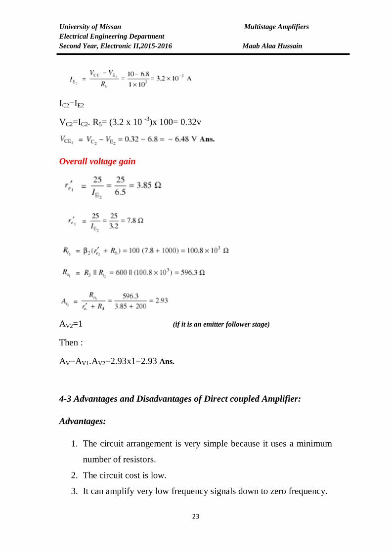
IC2=IE2
VC2=IC2. R5= (3.2 x 10 -3
)x 100= 0.32v
Overall voltage gain
AV2=1 (if it is an emitter follower stage)
Then :
AV=AV1.AV2=2.93x1=2.93 Ans.
4-3 Advantages and Disadvantages of Direct coupled Amplifier:
Advantages:
1. The circuit arrangement is very simple because it uses a minimum
number of resistors.
2. The circuit cost is low.
3. It can amplify very low frequency signals down to zero frequency.

University of Missan Multistage Amplifiers
Electrical Engineering Department
Second Year, Electronic II,2015-2016 Maab Alaa Hussain
24
Disadvantages:
1. It cannot amplify high frequency signals.
2. It has poor temperature stability. Because of this, its Q-point shifts.
In a multistage direct coupled amplifier, the Q-point shifts are
amplified in succeeding stages.
4-4 Application of Direct Coupled Amplifier:
The Direct Coupled Amplifier are used in many electronic system that
handle signals, which change very slowly with time. Some of the
important application are given below:
1. Analog computation.
2. Power supply regulators.
3. Bioelectric measurements.
4. Linear integrated circuits.
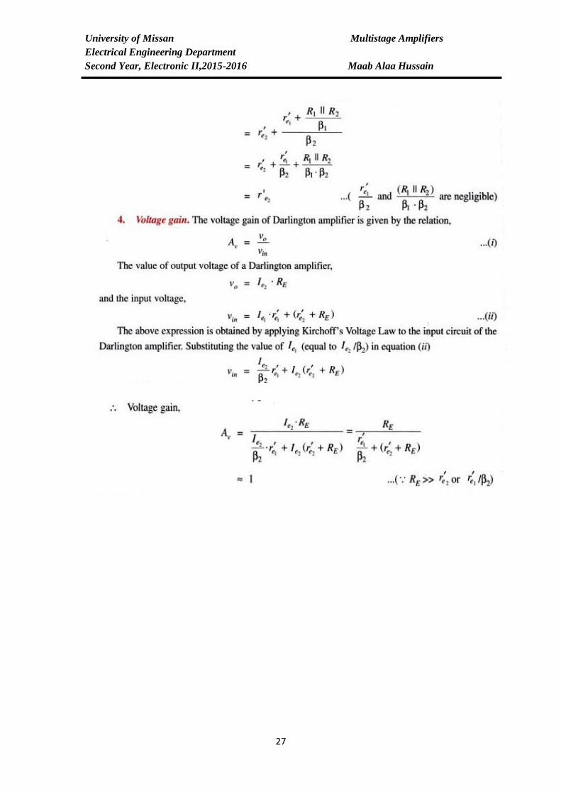
5- Darlington Amplifier:
The Darlington amplifier consists of two cascade emitter followers as
shown in Fig.(1-11). The darlington amplifier has a high input resistance,
low output resistance, and high current gain. These characteristics make it
very useful as a current amplifier. The voltage gain of this amplifier is
less than unity.
Fig.(1-11)

University of Missan Multistage Amplifiers
Electrical Engineering Department
Second Year, Electronic II,2015-2016 Maab Alaa Hussain
25
5-1 Darlington Amplifier Characteristics:
Consider the darligton amplifier circuit shown in Fig.(1-11).
Let Ib1= Base current of Q1 transistor,

University of Missan Multistage Amplifiers
Electrical Engineering Department
Second Year, Electronic II,2015-2016 Maab Alaa Hussain
26
University of Missan Multistage Amplifiers
Electrical Engineering Department
Second Year, Electronic II,2015-2016 Maab Alaa Hussain
27

University of Missan Multistage Amplifiers
Electrical Engineering Department
Second Year, Electronic II,2015-2016 Maab Alaa Hussain
28
Example:
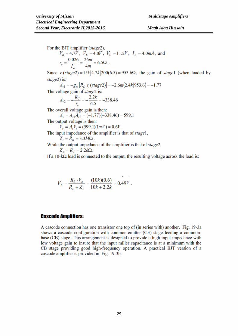
University of Missan Multistage Amplifiers
Electrical Engineering Department
Second Year, Electronic II,2015-2016 Maab Alaa Hussain
29

University of Missan Multistage Amplifiers
Electrical Engineering Department
Second Year, Electronic II,2015-2016 Maab Alaa Hussain
30
Example:

University of Missan Multistage Amplifiers
Electrical Engineering Department
Second Year, Electronic II,2015-2016 Maab Alaa Hussain
31

University of Missan Multistage Amplifiers
Electrical Engineering Department
Second Year, Electronic II,2015-2016 Maab Alaa Hussain
32
Tuned Amplifiers
1. Single-tuned voltage Amplifier:
Figure below shows the circuit of single-tuned voltage amplifier using
a bipolar junction transistor (BJT). The circuit in Fig. (a) is called
capacitively coupled tuned amplifier because the output is taken through
the coupling capacitor (Cc). similarly, the circuit shown in Fig. (b) is
called inductively coupled tuned amplifier because the output is taken
across an inductor. Both these circuits consists of a transistor amplifier
and tuned circuit as the load. The values of capacitance (C) and
inductance(L) of tuned circuit are selected in such a way that the resonant
frequency of the tuned circuit is equal to the frequency to be selected and
amplified. The resistors(R1, R2, and RE) are called biasing resistors. These
resistors provide d.c. operating currents and voltages for for the transistor.

University of Missan Multistage Amplifiers
Electrical Engineering Department
Second Year, Electronic II,2015-2016 Maab Alaa Hussain
33
As in the following figure:
2. Double-tuned Voltage Amplifier:
Figure bellow shows the circuit of a double tuned voltage amplifier. It
consist of a transistor amplifier with two tuned circuits. One of the tuned
(i.e., L1 C1) is shown as the collector load and other (i.e., L2 C2) as the
output. The resistor R1,R2 and RE are used to provided the d.c. currents
and voltages for the transistor operation.
The signal to be amplified is applied at the input terminal through the
coupling capacitor (Cc).
The resonant frequency of the tuned circuit L1C1 is made equal to that
of the signal (by adjusting L1 or C1). Under these conditions, the tuned
circuit offers a very high impedance to the input signal . As a result of

University of Missan Multistage Amplifiers
Electrical Engineering Department
Second Year, Electronic II,2015-2016 Maab Alaa Hussain
34
this, a large output appears across the tuned circuit L1C1. The output from
this tuned circuit is inductively coupled to the L2C2 tuned circuit.
The double tuned voltage amplifiers are extensively used in
intermediate frequency (IF) amplifier.