optical properties of high quality cu2znsnse4 thin films · where e d and e a are the donor and...
TRANSCRIPT

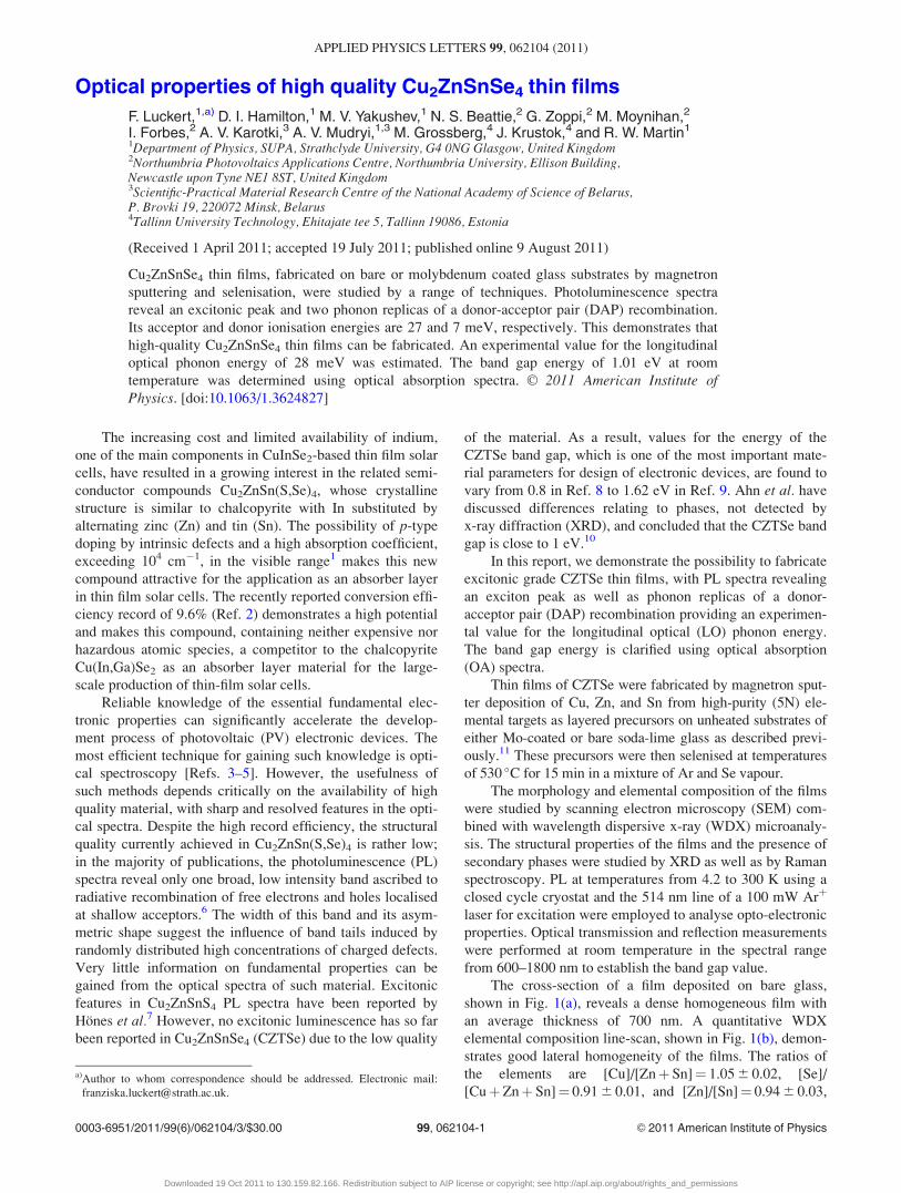
Optical properties of high quality Cu2ZnSnSe4 thin filmsF. Luckert, D. I. Hamilton, M. V. Yakushev, N. S. Beattie, G. Zoppi et al. Citation: Appl. Phys. Lett. 99, 062104 (2011); doi: 10.1063/1.3624827 View online: http://dx.doi.org/10.1063/1.3624827 View Table of Contents: http://apl.aip.org/resource/1/APPLAB/v99/i6 Published by the American Institute of Physics. Related ArticlesInfluence of copper excess on the absorber quality of CuInSe2 Appl. Phys. Lett. 99, 151912 (2011) The electronic structure of co-sputtered zinc indium tin oxide thin films J. Appl. Phys. 110, 073711 (2011) Temperature dependent phonon evolutions and optical properties of highly c-axis oriented CuGaO2semiconductor films grown by the sol-gel method Appl. Phys. Lett. 99, 131104 (2011) Communication: Uncovering molecule-TiO2 interactions with nonlinear spectroscopy J. Chem. Phys. 135, 081101 (2011) Organic conjugated material-based broadband terahertz wave modulators Appl. Phys. Lett. 99, 061108 (2011) Additional information on Appl. Phys. Lett.Journal Homepage: http://apl.aip.org/ Journal Information: http://apl.aip.org/about/about_the_journal Top downloads: http://apl.aip.org/features/most_downloaded Information for Authors: http://apl.aip.org/authors
Downloaded 19 Oct 2011 to 130.159.82.166. Redistribution subject to AIP license or copyright; see http://apl.aip.org/about/rights_and_permissions
Optical properties of high quality Cu2ZnSnSe4 thin films
F. Luckert,1,a) D. I. Hamilton,1 M. V. Yakushev,1 N. S. Beattie,2 G. Zoppi,2 M. Moynihan,2
I. Forbes,2 A. V. Karotki,3 A. V. Mudryi,1,3 M. Grossberg,4 J. Krustok,4 and R. W. Martin1
1Department of Physics, SUPA, Strathclyde University, G4 0NG Glasgow, United Kingdom2Northumbria Photovoltaics Applications Centre, Northumbria University, Ellison Building,Newcastle upon Tyne NE1 8ST, United Kingdom3Scientific-Practical Material Research Centre of the National Academy of Science of Belarus,P. Brovki 19, 220072 Minsk, Belarus4Tallinn University Technology, Ehitajate tee 5, Tallinn 19086, Estonia
(Received 1 April 2011; accepted 19 July 2011; published online 9 August 2011)
Cu2ZnSnSe4 thin films, fabricated on bare or molybdenum coated glass substrates by magnetron
sputtering and selenisation, were studied by a range of techniques. Photoluminescence spectra
reveal an excitonic peak and two phonon replicas of a donor-acceptor pair (DAP) recombination.
Its acceptor and donor ionisation energies are 27 and 7 meV, respectively. This demonstrates that
high-quality Cu2ZnSnSe4 thin films can be fabricated. An experimental value for the longitudinal
optical phonon energy of 28 meV was estimated. The band gap energy of 1.01 eV at room
temperature was determined using optical absorption spectra. VC 2011 American Institute ofPhysics. [doi:10.1063/1.3624827]
The increasing cost and limited availability of indium,
one of the main components in CuInSe2-based thin film solar
cells, have resulted in a growing interest in the related semi-
conductor compounds Cu2ZnSn(S,Se)4, whose crystalline
structure is similar to chalcopyrite with In substituted by
alternating zinc (Zn) and tin (Sn). The possibility of p-type
doping by intrinsic defects and a high absorption coefficient,
exceeding 104 cm�1, in the visible range1 makes this new
compound attractive for the application as an absorber layer
in thin film solar cells. The recently reported conversion effi-
ciency record of 9.6% (Ref. 2) demonstrates a high potential
and makes this compound, containing neither expensive nor
hazardous atomic species, a competitor to the chalcopyrite
Cu(In,Ga)Se2 as an absorber layer material for the large-
scale production of thin-film solar cells.
Reliable knowledge of the essential fundamental elec-
tronic properties can significantly accelerate the develop-
ment process of photovoltaic (PV) electronic devices. The
most efficient technique for gaining such knowledge is opti-
cal spectroscopy [Refs. 3–5]. However, the usefulness of
such methods depends critically on the availability of high
quality material, with sharp and resolved features in the opti-
cal spectra. Despite the high record efficiency, the structural
quality currently achieved in Cu2ZnSn(S,Se)4 is rather low;
in the majority of publications, the photoluminescence (PL)
spectra reveal only one broad, low intensity band ascribed to
radiative recombination of free electrons and holes localised
at shallow acceptors.6 The width of this band and its asym-
metric shape suggest the influence of band tails induced by
randomly distributed high concentrations of charged defects.
Very little information on fundamental properties can be
gained from the optical spectra of such material. Excitonic
features in Cu2ZnSnS4 PL spectra have been reported by
Hones et al.7 However, no excitonic luminescence has so far
been reported in Cu2ZnSnSe4 (CZTSe) due to the low quality
of the material. As a result, values for the energy of the
CZTSe band gap, which is one of the most important mate-
rial parameters for design of electronic devices, are found to
vary from 0.8 in Ref. 8 to 1.62 eV in Ref. 9. Ahn et al. have
discussed differences relating to phases, not detected by
x-ray diffraction (XRD), and concluded that the CZTSe band
gap is close to 1 eV.10
In this report, we demonstrate the possibility to fabricate
excitonic grade CZTSe thin films, with PL spectra revealing
an exciton peak as well as phonon replicas of a donor-
acceptor pair (DAP) recombination providing an experimen-
tal value for the longitudinal optical (LO) phonon energy.
The band gap energy is clarified using optical absorption
(OA) spectra.
Thin films of CZTSe were fabricated by magnetron sput-
ter deposition of Cu, Zn, and Sn from high-purity (5N) ele-
mental targets as layered precursors on unheated substrates of
either Mo-coated or bare soda-lime glass as described previ-
ously.11 These precursors were then selenised at temperatures
of 530 �C for 15 min in a mixture of Ar and Se vapour.
The morphology and elemental composition of the films
were studied by scanning electron microscopy (SEM) com-
bined with wavelength dispersive x-ray (WDX) microanaly-
sis. The structural properties of the films and the presence of
secondary phases were studied by XRD as well as by Raman
spectroscopy. PL at temperatures from 4.2 to 300 K using a
closed cycle cryostat and the 514 nm line of a 100 mW Arþ
laser for excitation were employed to analyse opto-electronic
properties. Optical transmission and reflection measurements
were performed at room temperature in the spectral range
from 600–1800 nm to establish the band gap value.
The cross-section of a film deposited on bare glass,
shown in Fig. 1(a), reveals a dense homogeneous film with
an average thickness of 700 nm. A quantitative WDX
elemental composition line-scan, shown in Fig. 1(b), demon-
strates good lateral homogeneity of the films. The ratios of
the elements are [Cu]/[ZnþSn]¼ 1.05 6 0.02, [Se]/
[CuþZnþ Sn]¼ 0.91 6 0.01, and [Zn]/[Sn]¼ 0.94 6 0.03,
a)Author to whom correspondence should be addressed. Electronic mail:
0003-6951/2011/99(6)/062104/3/$30.00 VC 2011 American Institute of Physics99, 062104-1
APPLIED PHYSICS LETTERS 99, 062104 (2011)
Downloaded 19 Oct 2011 to 130.159.82.166. Redistribution subject to AIP license or copyright; see http://apl.aip.org/about/rights_and_permissions

indicating a small excess of copper as well as a deficiency of
zinc and selenium.
Figure 1(c) shows the XRD spectrum of the CZTSe film
on Mo on a logarithmic scale to highlight possible low inten-
sity peaks. The spectrum reveals several distinct CZTSe
peaks, a strong molybdenum peak, and two low intensity
MoSe2 peaks. These peaks imply that the selenisation reac-
tion has continued through the precursor layer reaching the
molybdenum substrate.
In the room temperature Raman spectra of the films on
bare glass and Mo, shown in Fig. 1(d), the modes at 169,
173, 196.6, and 234 cm�1, as reported earlier in Ref. 6 and
assigned to CZTSe, can be seen. The Cu2�xSe mode at 261
cm�1, identified earlier,12 can also be found at a few small
spots randomly distributed across the surface. However, the
main part of the surface was found to be free from secondary
phases.
The 242 cm�1 Raman line associated with MoSe2 has
rather low intensity when measured at the top of a dense, ho-
mogeneous film. Its intensity increases significantly (not
shown here) when the laser beam is focused closer to the Mo
layer suggesting that the MoSe2 phase is present mainly at
the Mo/CZTSe interface. The formation of the MoSe2 phase
has also been reported in Ref. 10 at the Mo/CZTSe interface
after selenisation at 500 �C. None of the other secondary
phases reported in Ref. 6 were observed in the Raman spec-
tra of the CZTSe thin film.
The full width at half maximum (FWHM) of the domi-
nant A1 mode is 3 cm�1. This is significantly smaller than
the 10 cm�1 estimated in the Raman spectrum, reported by
Ahn et al.,10 and suggests superior structural quality for our
material. In order to clarify the band gap energy, room tem-
perature optical absorption a(hm) has been calculated using
both optical transmission and reflection data.13 For an
allowed direct transition, the spectral dependence of the
absorption coefficient can be calculated as a¼A(hm�Eg)1/2/hm (Ref. 14) with constant A and optical band gap energy Eg.
Fig. 3(a) plots a room temperature dependence of (ahm)2 on
photon energy hm. The optical band gap of Eg¼ 1.01 eV has
been determined by extrapolating the linear part of the
(ahm)2 dependence to the photon energy axis. This value is in
good agreement with those determined experimentally by
Ahn et al. in Ref. 10 and Grossberg et al. in Ref. 6 as well as
theoretically by Chen et al.15
Figure 2(b) shows the evolution of the near band edge
PL spectra with changing excitation intensity. At 4.5 K, the
PL spectra are dominated by a relatively narrow PL band at
0.989 eV (DAP) and the two lower intensity bands at 0.963
eV (DAP1LO) and 0.932 eV (DAP2LO). In order to determine
their spectral positions and integrated intensity, the experi-
mental data points of the DAP, DAP1LO, and DAP2LO have
been fitted by three Gaussians. A small blue shift at a rate of
2.9 meV/decade, with increasing excitation power, suggests
that the DAP peak originates from a donor-acceptor pair
recombination.16
The integrated PL intensity of the DAP band increases
with increasing excitation power P as I � Pc, with the power
coefficient c � 0.63, suggesting that this band is due to
defect related transitions.17 The spectral position of the DAP
band maximum hmmax can be described as
hmmax ¼ Eg � ðEd þ EaÞ þe2
ð4pe0erÞ; (1)
FIG. 1. (Color online) (a) Cross sectional SEM micrograph of a CZTSe film
on glass, (b) WDX linescan, (c) XRD pattern of a CZTSe film on Mo, and
(d) Raman spectra of the CZTSe thin films on glass and Mo.
FIG. 3. (Color online) Temperature dependence of the PL spectra (a), tem-
perature quenching of the integrated intensity of the DAP peak (*, experi-
mental points; -, fitted lines) (b), and dependence of the DAP peak spectral
position on temperature (c).
FIG. 2. (Color online) Room temperature dependence of (ahm)2 on photon
energy hm (a), evolution of the PL spectrum with increasing excitation power
P (b), and excitation power dependence of the EX peak at 5 K (c).
062104-2 Luckert et al. Appl. Phys. Lett. 99, 062104 (2011)
Downloaded 19 Oct 2011 to 130.159.82.166. Redistribution subject to AIP license or copyright; see http://apl.aip.org/about/rights_and_permissions

where Ed and Ea are the donor and acceptor ionisation ener-
gies, respectively, r is the distance between the donor and
acceptor, e is the electron charge, e is the static dielectric con-
stant, and e0 is the permittivity of vacuum. The last term of
Eq. (1) describes the Coulomb interaction between the donor
and acceptor like defects. As the excitation power increases,
the concentration of occupied donor and acceptor centres also
increases, reducing the average distance between these defects
resulting in a higher Coulomb interaction energy and a shift of
the band towards higher energy.
The spectral positions of the two lower intensity bands
DAP1LO and DAP2LO also shift towards higher energies with
increasing excitation power at the same rate as the DAP band
(2.9 meV/decade). The spectral distance between the DAP and
the DAP1LO bands as well as between the DAP1LO and
DAP2LO bands is about �28 meV, which is close to the LO
phonon energy in the chalcopyrite CuInSe2.18 Therefore,
DAP1LO and DAP2LO can be assigned to phonon-assisted DAP
recombination with a LO phonon energy of ELO¼ 28 6 2
meV (226 6 16 cm�1). The experimental uncertainty of deter-
mining the spectral position of the DAP bands in the PL spec-
tra is such that the Raman line associated with LO phonons
could be merged with the broad feature at 234 cm�1.
The PL spectra, shown in Fig. 2(b), also reveal a high-
energy feature (labelled EX) at �1.033 eV. This feature can
better be seen at higher excitation intensities and, as shown
in Fig. 2(c), does not exhibit any shift with varying excitation
power. The spectral position and the excitation power de-
pendent behaviour of the EX feature suggest that this band
can be attributed to a recombination of excitons. The evolu-
tion of the PL spectra with temperature increasing from 5 to
60 K is shown in Fig. 3(a). The intensity of all PL bands
decreases. This temperature quenching is due to the ther-
mally activated depopulation of the defect energy levels or/
and to the activation of a non-radiative recombination centre.
An Arrhenius plot can be used to determine activation ener-
gies Ea of the process. The exciton peak is quenching at
around 13 K which makes it impossible to determine an acti-
vation energy value. The width and the quenching character
of this feature suggest that it consists of non-resolved free
and bound excitons.
Since the excitonic feature has been observed at liquid
helium temperature, whereas the band gap measurements
were carried out at room temperature, we cannot estimate
the binding energy of the exciton. However, it is clear that
the low temperature band gap energy should be quite close
to the energy of the excitonic peak at 1.033 eV. The same
low temperature band gap energy was recently confirmed by
the temperature dependence of quantum efficiency spectra of
CZTSe solar cells.19
The temperature quenching dependence of the inte-
grated PL intensity for T> 10 K of the DAP band is shown
in Fig. 3(b). The best fit of the experimental data points has
been achieved assuming two activation energies,20
IðTÞ ¼ I0= 1þ A1exp �Ea1
kT
� �þ A2exp �Ea2
kT
� �� �; (2)
where I0 (the intensity at the lowest temperature), Ea (activa-
tion energies), and A are fitting parameters (k is the Boltz-
mann constant). The determined activation energies are
Ea1¼ 27 6 3 meV and Ea2¼ 7 6 2 meV. We propose a DAP
model of recombination including an acceptor and a donor.
With the temperatures increase, the DAP peak is becoming
narrower and gradually shifting to higher energies due to the
ionisation of the donor with an energy level 7 meV below
the conduction band. The DAP recombination transforms
into a recombination of an electron from the conduction
band and a hole localised at the acceptor with an energy level
27 meV above the valence band.
In conclusion, CZTSe thin films have been studied by
WDX, XRD, Raman, OA, and temperature resolved PL. The
XRD and Raman spectra demonstrate high structural quality
of the material. The band gap value, determined by optical
absorption analysis at room temperature, was found to be
close to 1 eV. The temperature quenching analysis of the
dominating high-intensity and relatively narrow DAP band
suggests that it is associated with the optical transitions
between an acceptor at 27 meV above the valence band and
a donor at 7 meV below the conduction band. Two phonon
replicas of the DAP band and an excitonic feature have been
observed in the PL spectra. An experimental LO phonon
energy of �28 meV was determined.
This work was supported by the EPSRC, Materials in
Engineering (4.5.01) and SUPERGEN programme
“Photovoltaics for the 21st Century,” BCFR (F11MC-021),
RFBR (10-03-96047 and 11-03-00063), and Estonian Sci-
ence Foundation (G-8282).
1K. Ito and T. Nakazawa, Jpn. J. Appl. Phys. 27, 2094 (1988).2T. K. Todorov, K. B. Reuter, and D. B. Mitzi, Adv. Mater. 22, 1 (2010).3M. V. Yakushev, A. V. Mudryi, I. V. Victorov, J. Krustok, and E. Melli-
kov, Appl. Phys. Lett. 88, 011922 (2006).4M. V. Yakushev, F. Luckert, C. Faugeras, A. V. Karotki, A. V. Mudryi,
and R. W. Martin, Appl. Phys. Lett. 97, 152110 (2010).5F. Luckert, M. V. Yakushev, C. Faugeras, A. V. Karotki, A. V. Mudryi,
and R. W. Martin, Appl. Phys. Lett. 97, 162101 (2010).6M. Grossberg, J. Krustok, K. Timmo, and M. Altosaar, Thin Solid Films
517, 2489 (2009).7K. Hones, E. Zscherpel, J. Scragg, and S. Siebentritt, Physica B 404, 4949
(2009).8T. M. Friedlmeier, N. Wieser, T. Walter, H. Dittrich, and H. W. Schock,
Proceedings of the 14th European Photovotlaic Specialists Conference,Barcelona (H.S. Stephens & Ass., Bedford, UK, 1997), p. 1242.
9G. S. Babu, Y. B. K. Kumar, P. U. Bhaskar, and S. R. Vanjari, Sol. Energy
Mater. Sol. Cells 94, 221 (2010).10S. Ahn, S. Jung, J. Gwak, A. Cho, K. Shin, K. Yoon, D. Park, H. Cheong,
and J. H. Yun, Appl. Phys. Lett. 97, 021905 (2010).11G. Zoppi, I. Forbes, R. W. Miles, P. J. Dale, J. J. Scragg, and L. M. Peter,
Prog. Photovoltaics 17, 315 (2009).12G. Morell, R. S. Katiyar, S. Z. Weisz, T. Walter, H. W. Schock, and I. Bal-
berg, Appl. Phys. Lett. 69, 987 (1996).13A. V. Mudryi, V. F. Gremenok, I. A. Victorov, V. B. Zalesski, F. V. Kur-
desov, V. I. Kovalevski, M. V. Yakushev, and R. W. Martin, Thin Solid
Films 431/432, 193 (2003).14J. I. Pankove, Optical Processes in Semiconductors (Dover, New York,
1975).15S. Y. Chen, X. G. Gong, A. Walsh, and S. H. Wei, Appl. Phys. Lett. 94,
041903 (2009).16R. Dingle, Phys. Rev. 184, 788 (1969).17T. Schmidt, K. Lischka, and W. Zulehner, Phys. Rev. B 45, 8989 (1992).18H. Tanino, T. Maeda, H. Fujikake, H. Nakanishi, S. Endo, and T. Irie,
Phys. Rev. B 45, 13323 (1992).19J. Krustok, R. Josepson, T. Raadik, and M. Danilson, Physica B 405, 3186
(2010).20J. Krustok, H. Collan, and K. Hjelt, J. Appl. Phys. 81, 1442 (1997).
062104-3 Luckert et al. Appl. Phys. Lett. 99, 062104 (2011)
Downloaded 19 Oct 2011 to 130.159.82.166. Redistribution subject to AIP license or copyright; see http://apl.aip.org/about/rights_and_permissions