nextpower mosfets - farnell element14 six most important mosfet parameters required for...
TRANSCRIPT

NextPower MOSFETsSmaller, Faster, Cooler

2 NextPower MOSFETs - Visit us at www.nxp.com/mosfets
NextPower 25 V & 30 V MOSFETsin LFPAK (Power-SO8)
NXP introduces a range of high performance N-channel, logic-level MOSFETs in LFPAK
As a power design engineer, compromise is never far from your mind. Do I choose a low RDS(on) device and accept the higher output capacitance? Do I demand the lowest gate charge characteristics to reduce switching losses but then find that the package options are no longer ideal in my application?
The NextPower range of MOSFETs from NXP provides uniquely balanced characteristics across the six most important parameters essential for your latest high efficiency and high reliability designs. More performance, less compromise…
Many competitors focus only on optimising RDS(on) and Qg. As Qg gets lower then losses due to Qoss and Qgd become more significant. NextPower uses Superjunction technology to provide the optimum balance between low RDS(on), low Qoss, low Qg(tot) and Qgd to give optimum switching performance. NextPower delivers superior SOA performance, and low Qoss reduces the losses between the output DRAIN & SOURCE terminals. NextPower also delivers the lowest RDS(on) with sub 1 mΩ types at both 25 V and 30 V.
LFPAK packaging provides rugged power switching on a compact 5 mm x 6 mm footprint compatible with other Power-SO8 vendors. The unique benefits of LFPAK make it the best package choice for demanding applications or where high-reliability is required. It also allows for visual inspection, reducing the need for costly X-ray equipment to detect solder defects as is common with QFN style Power-SO8 packages.
Key benefits High efficiency in power switching applications Industry’s lowest RDS(on) Power-SO8 - Less than 1 mΩ
at 25 V and 30 V Low Qoss for reduced output losses between DRAIN &
SOURCE Low Qgd for reduced switching losses and high frequency
switching 20 V rated GATE provides better tolerance to voltage
transients than lateral MOSFET types Superior ‘Safe Operating Area’ performance compared
to other Trench MOSFET vendors Optimised for 4.5 V gate drive voltage
Optimum switching performance under light & heavy load conditions
LFPAK package for compatibility with other vendor Power-SO8 types
Eliminates costly X-ray inspection – LFPAK solder joints can be optically inspected
Key applications Synchronous buck regulators DC-DC conversion Voltage regulator modules (VRM) Power OR-ing

3NextPower MOSFETs - Visit us at www.nxp.com/mosfets
NextPower 25 V & 30 V MOSFETsin LFPAK (Power-SO8)
Benefits of Superjunction technology
Many suppliers focus on two favourable indicators when defining MOSFET performance, but this only tells part of the story.
The spider chart below shows the relative performance of NextPower versus the leading MOSFET vendors, comparing the six most important MOSFET parameters required for high-performance & high reliability switching applications. The outside edge of the graph represents the ‘best-in-class’ performance, whilst scoring towards the centre of the graph represents a weakness.
Low RDS(on) gives low I2R losses and superior performance when used in a SYNC FET or power OR-ing application
Low Qoss gives reduced losses between the drain& source terminals since the energy stored in the output capacitance (Coss) is wasted whenever the voltage changes across the output terminals
SOA performance provides tolerance to overload & fault conditions. The graph shows the maximum allowable current for a 1 mS pulse at VDS=10 V
Low Miller charge (QGD) gives reduced switching losses between the MOSFET’s drain & source terminals when the MOSFET turns ON or turns OFF
Low gate charge (QG) gives reduced losses in the gate drive circuit since less energy is required to turn the MOSFET ON & OFF
Superior junction temperature rating, Tj(max), is proof that LFPAK is the most rugged Power-SO8 package available. LFPAK is the best choice for demanding environments and where high reliability is required
Comparison of NextPower technology with key competitor types
RDS(on)max@ Vgs = 4.5 V
Tj(max) NXP
Competitor A
Competitor B
Combined QG & QGD FOM SOA rating
Qoss FOM
4 NextPower MOSFETs - Visit us at www.nxp.com/mosfets
NextPower types – parametric data
The 25 V and 30 V types shown below are recommended for synchronous buck regulators, the low RDS(on) types are also highly recommended for Power OR-ing applications and low voltage isolated power supply topologies.
Type Voltage (V)RDS(on)typ
VGS = 4.5 V (mΩ)QG(typ)
VGS = 4.5 V (nC)QGD(typ)
VGS = 4.5 V (nC)COSS (pF)
PSMN0R9-25YLC 25 0.95 51 14 1437
PSMN1R1-25YLC 25 1.2 39 11 1121
PSMN1R2-25YLC 25 1.35 31 8.3 994
PSMN1R7-25YLC 25 2 28 7.8 880
PSMN1R9-25YLC 25 2.2 27 7.4 761
PSMN2R2-25YLC 25 2.6 18 5.2 617
PSMN2R9-25YLC 25 3.45 16 4.4 501
PSMN3R2-25YLC 25 3.7 14 4 462
PSMN3R7-25YLC 25 4.25 10.1 3 370
PSMN4R0-25YLC 25 4.5 10.9 3.5 354
25 V NextPower types
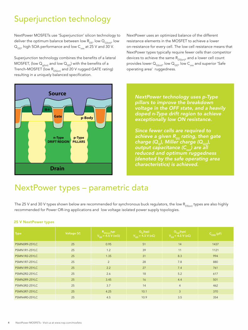
NextPower MOSFETs use ‘Superjunction’ silicon technology to deliver the optimum balance between low RDS, low QG(tot), low QGD, high SOA performance and low Coss at 25 V and 30 V.
Superjunction technology combines the benefits of a lateral MOSFET, (low Qg(tot) and low QGD) with the benefits of a Trench-MOSFET (low RDS(on) and 20 V rugged GATE rating) resulting in a uniquely balanced specification.
NextPower uses an optimized balance of the different resistance elements in the MOSFET to achieve a lower on-resistance for every cell. The low cell resistance means that NextPower types typically require fewer cells than competitor devices to achieve the same RDS(on), and a lower cell count provides lower QG(tot), low QGD, low Coss and superior ‘Safe operating area’ ruggedness.
NextPower technology uses p-Type pillars to improve the breakdown voltage in the OFF state, and a heavily doped n-Type drift region to achieve exceptionally low ON resistance.
Since fewer cells are required to achieve a given RDS rating, then gate charge (QG), Miller charge (QGD), output capacitance (Coss) are all reduced and optimum ruggedness (denoted by the safe operating area characteristics) is achieved.
Superjunction technology
Drain
p-TypePILLARS
n-TypeDRIFT REGION
n+
Gate p-Body
Source
5NextPower MOSFETs - Visit us at www.nxp.com/mosfets
Type Voltage (V)RDS(on)typ
VGS = 4.5 V (mΩ)QG(typ)
VGS = 4.5 V (nC)QGD(typ)
VGS = 4.5 V (nC)COSS (pF)
PSMN1R0-30YLC 30 1.1 50 14.6 1210
PSMN1R2-30YLC 30 1.35 38 11.6 977
PSMN1R5-30YLC 30 1.65 30 8.6 860
PSMN2R2-30YLC 30 2.3 26 8 651
PSMN2R6-30YLC 30 3.1 18 5.5 549
PSMN3R2-30YLC 30 3.75 14.2 4.1 432
PSMN3R7-30YLC 30 4.25 14 4.2 380
PSMN4R1-30YLC 30 4.75 11 3.5 316
PSMN4R5-30YLC 30 5.1 9.6 2.85 288
30 V NextPower types
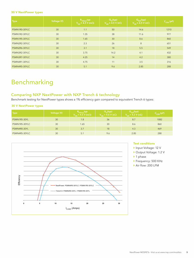
Benchmarking
Comparing NXP NextPower with NXP Trench 6 technology Benchmark testing for NextPower types shows a 1% efficiency gain compared to equivalent Trench 6 types:
Test conditions Input Voltage: 12 V Output Voltage: 1.2 V 1 phase Frequency: 500 KHz Air flow: 200 LFM
Type Voltage (V)RDS(on)typ
VGS = 4.5 V (mΩ)QG(typ)
VGS = 4.5 V (nC)QGD(typ)
VGS = 4.5 V (nC)COSS (pF)
PSMN1R5-30YL 30 1.8 36 8.7 1082
PSMN1R5-30YLC 30 1.65 30 8.6 860
PSMN4R0-30YL 30 3.7 18 4.3 469
PSMN4R5-30YLC 30 5.1 9.6 2.85 288
30 V NextPower types=&G$3H") IJ0C&4E$F9)=K,LMN<=)
OKC$F9E)=K,LMN<=)
OKPC$F9E)=K,LMN<=)
8+,,C$F9E )
XYW! U5V! Uf! V5f! TVVY!XYW! U5X! U\! ] ! \VT!
XYW! ] ! f5f ! U5]! bgf !XYW! V5T! f5\! U5]V! U]] !
0 5 10 15 20 25 30
NextPower: PSMN4R5-30YLC / PSMN1R5-30YLC
Trench 6: PSMN4R0-30YL / PSMN1R5-30YL
Effi
cien
cy
ILOAD (Amps)

6 NextPower MOSFETs - Visit us at www.nxp.com/mosfets
Comparing NextPower with a leading competitor Benchmarking tests show that NextPower types deliver 1% efficiency gains compared to the nearest competitor types:
Test conditions Input Voltage: 12 V Output Voltage: 1.2 V 1 phase Frequency: 500 KHz Air flow: 200 LFM
0 5 10 15 20 25 30
PSMN4R0-25YLC/PSMN1R1-25YLC
Competitor
Effi
cien
cy
ILOAD (Amps)
Safe Operating Area comparison
0
1
2
3
4
5
6
7
8
9
10
NXP Trench 6 and previous generationfrom competition
NXP NextPower and latest generationfrom competition
NXP
SO
A C
urre
nt (A
mp)
Competitor 1
Competitor 2
Condition: SOA Drain current (Amp) @ Vds=10 V, 10 ms pulse for a 5 mΩ (@ 10 V) in Power SO8
Why Choose LFPAK? Reduced electrical resistance and inductance Outstanding thermal performance Rugged design, qualified to AEC-Q101
(stringent automotive standard) Easy to handle, solder and inspect Power-SO8 footprint compatible

7NextPower MOSFETs - Visit us at www.nxp.com/mosfets
NextPower types - Coming in Q3-2011
Further NextPower types are planned for release in Q3-2011. Preliminary data is provided in the tables below. These types are recommended for control-FET applications in synchronous-buck regulators. YLB types have an integrated snubber circuit to further reduce spiking levels for critical applications.
Type Voltage (V)RDS(on)typ
VGS = 4.5 V (mΩ)
PSMN5R0-25YLB 25 6.1
PSMN5R0-25YLC 25 6.6
PSMN6R0-25YLC 25 7.3
PSMN7R3-25YLC 25 8.9
PSMN9R0-25YLC 25 10.7
PSMN011-25YLC 25 12.7
Type Voltage (V)RDS(on)typ
VGS = 4.5 V (mΩ)
PSMN6R0-30YLB 30 6.7
PSMN6R0-30YLC 30 7.6
PSMN7R0-30YLC 30 8.5
PSMN8R6-30YLC 30 10.3
PSMN011-30YLC 30 11.7
PSMN012-30YLC 30 13.8
MOSFET BRAND NAME
MOSFET type
N-ch or P-ch
MOSFETon-resistance
RDS(on)
-MOSFET voltage
BVDSPackage type
Gate threshold voltage
NextPower special features
P S M N 1 R 7 - 25 Y L C
Power Silicon Max
N = N-ch R95 = 0.95 mΩ - 25 = 25 VB = D2PAKSOT404
L = Logic-levelC = Optimised
for Qg(fom)
P = P-ch 1R7 = 1.7 mΩ - 30 = 30 VD = DPAKSOT428
S = Standard-levelB = integrated
snubber
X =Dual N-ch
014 = 14 mΩ - 40 = 40 VE = I2PAKSOT226
Y =Dual P-ch
125 = 125 mΩ - 60 = 60 VK = SO8SOT96
Z =N-ch + P-ch
- 80 = 80 VL = QFN3333
SOT873
- 100 = 100 VP = TO220
SOT78
- 110 = 110 VY = LFPAKSOT669 & SOT1023
- 120 = 120 VX = TO220F (FULLPACK)SOT186A
Part numbering for NXP MOSFETs
types in bold red italic underline represent products in development
© 2011 NXP Semiconductors N.V.
All rights reserved. Reproduction in whole or in part is prohibited without the prior written consent of the
copyright owner. The information presented in this document does not form part of any quotation or contract,
is believed to be accurate and reliable and may be changed without notice. No liability will be accepted by
the publisher for any consequence of its use. Publication thereof does not convey nor imply any license under
patent- or other industrial or intellectual property rights.
www.nxp.com
Date of release: May 2011
Document order number: 9397 750 17100
Printed in the Netherlands