new england ip transition conference - massachusetts
TRANSCRIPT

Corresponding author: [email protected] University of Wales Swansea Singlton Park, SA2 8PP Swansea, UK Tel: ++44 1792 513548/Fax: ++44 1792 295221 Copyright © JES 2005 on-line : journal.esrgroups.org/jes
Z. Zhou M. S. Khanniche P. Igic S. M. Towers P. A. Mawby
J. Electrical Systems 1-4 (2005): 33-46
Regular paper
Power Loss Calculation and Thermal Modelling for a Three Phase Inverter Drive System
JES
Journal of Electrical Systems
Power losses calculation and thermal modelling for a three-phase inverter power system is presented in this paper. Aiming a long real time thermal simulation, an accurate average power losses calculation based on PWM reconstruction technique is proposed. For carrying out the thermal simulation, a compact thermal model for a three-phase inverter power module is built. The thermal interference of adjacent heat sources is analysed using 3D thermal simulation. The proposed model can provide accurate power losses with a large simulation time-step and suitable for a long real time thermal simulation for a three phase inverter drive system for hybrid vehicle applications.
Keywords: power losses; thermal modelling; inverter drive system; PWM reconstruction, IGBT junction temperature.
1. INTRODUCTION
Inverter Power Modules (IPM) based on Insulated gate bipolar transistors (IGBT) power modules, are more and more popular for automotive industry. However, due to the confined volumes and high temperature environment, high power density and huge power dissipation, make the power package exposed to high thermal constraints, especially in system transients and very harsh electrical environments [1]. Since the reliability of the power modular very depend on the device junction operating temperature, so effective power losses and thermal simulation is necessary for designer.
A accurate approach to determine the losses is to simulate a circuit by using physically matched device model [2-4], however, due to the complicate physical switching process, the determination of power losses and thermal performance need a very detailed device model and very small simulation time steps, this will result in a massive computing time and memory requirement for a complex power electronics system, especially in the case of long real time electro-thermal simulations. Another approach to determine the losses is to calculate the power losses analytically by using device data sheet provided from manufactures [8]. This method is simple, but less accurate.

Z. Zhou et al: Loss Calculation and Thermal Modelling for 3 Phase Inverter...
34
To overcome the difficulties, a novel power losses calculation method for a three-phase inverter power module thermal simulation using PWM reconstruction technique is presented in this paper. Initially a temperature-dependent conducting and switching characteristics of power devices are set up by measurement, in which, the turn-on and turn-off switching losses are represented as a function of device voltage, current, and junction temperature.
Next, a system level of the complete inverter drive electrical simulation and temperature coupled power losses and power module thermal simulation are carried out. Here the key feature that allows a significant speed-up of the simulation CPU time is this simplified representation of the inverter during the system level modelling. We have taken the approach that the inverter can be described by a unity gain amplifier. This allows the system to work on effective voltages and currents, which are continuous quantities (rather than the actual PWM switching waveforms). By using PWM reconstruction technique, device current in time-domain can be reconstructed and accurate power losses and thermal simulation can be carried out.
2. TEMPERATURE DEPENDENT POWER LOSSES CHARACTERISTICS OF POWER DEVICES
The power loss of each PWM switching cycle for each power device is divided into conduction losses, turn on loss and turn off loss, the total power loss is the sum of these three portions.
For an IGBT power device, the conduction loss can be calculated using the device collect current and the forward saturation voltage by
_ ( ) ( ) ( )cond loss ce cP t V t i t= (1)
where ceV , ci represent the forward saturation voltage, collector current of an IGBT, respectively. The measured ce cV I− characteristic of the IGBT is shown in Figure 1. It can be seen that the saturation voltage ceV is a function of collect current and junction temperature.
( ) ( ( ), ( ))ce cont c jV t f i t T t= (2)
where jT represents the junction operating temperature. In an inverter drive system, where significant inductance exists in load circuit, it is reasonable to assume the conduction current being constant over the on-time period of each switching cycle. So base on this assumption, the average conduction loss of each PWM switching pulse can be calculated by:

J. Electrical Systems 1-4 (2005): 33-46
35
_1( ) ( ) ( ) ( )cond ave ce c onsw
P k V k i k t kT
≈ (3)
where, ont , represents the conduction time; k denotes the thk PWM switching cycle. The same method can be applied for calculating conduction loss of power diodes.
Ic (A)
0 0.2 0.4 0.6 0.8 1 1.2 1.4 1.6 1.8 20
50
100
150
Vce (V)
VGE=15V
Tj=150oC
Tj=100oC
Tj=50oC
Figure 1: Measured ce cV I− characteristics of an IGBT at different temperature
Figure 2: IGBT total switching energy losses characteristics
Due to the complicated physics process of switching. In this paper, a lookup-table method is utilised, in which, the switching energy loss is defined as a function of collect current and junction temperature (for a constant dc link voltage). The function is represented as

Z. Zhou et al: Loss Calculation and Thermal Modelling for 3 Phase Inverter...
36
( ) ( ( ), ( ))sw on sw on c jE k f i k T k− −= (4)
( ) ( ( ), ( ))sw off sw off c jE k f i k T k− −= (5)
The total switching loss is calculated by
( ) ( ) ( )sw sw on sw offE k E k E k− −= + (6)
and represented as
( ) ( ( ), ( ))sw k sw c jE f i k T k= (7)
where, k denotes the thk PWM switching pluse. The measured total IGBT switching energy losses against collect current and junction temperature is shown in Figure 2. It can be seen that the total switching energy loss increases with increase of collect current and junction temperature, and can be considered as a function of the collect current and junction temperature The average switching power loss of a switching cycle is then calculated by
_1( ) ( )sw ave swsw
P k E kT
= (8)
If the dc link voltage is changed, the the switching losse characteristics will vary to reflect this change. Adding Eq. (3) and (8), the average power loss
_ave lossP over each switching cycle is calculated by
_ _ _( ) ( ) ( )ave loss sw ave cond aveP k P k P k= + (9)
3. PWM AND DEVICE CURRENT RECONSTRUCTION FOR POWER LOSSES CALCULATION
The simulation in Figure 3 gives the effective motor voltages and currents, which are continuous quantities (rather than the actual PWM switching waveforms) and cannot directly be used for power losses calculation. Therefore, a PWM reconstruction technique is proposed for the power losses simulation. By using PWM reconstruction technique, device current and the on-time of device can be mathematically reconstructed for power losses calculation. Figure 3 shows the block diagram of the PWM and device current reconstruction.
where, mV and mI are the effective motor terminal voltage and current vectors. The mathematical method to reconstruct the PWM signals will depend on the actual PWM strategy applied. Figure 4 shows a three-phase PWM inverter circuit.

J. Electrical Systems 1-4 (2005): 33-46
37
Im
Ic Vm PWM signals reconstruction
PWM Device current reconstruction
Figure 3: PWM signals and device conduction current reconstruction process using
effective smooth motor stator voltage vector
S2 S3
S4 S5 S6
S1
Vdc
+DC
-DC
ima
imb
imc
T1 T2 T3
T4 T5 T6
D1 D2 D3
D4 D5 D6
Figure 4: A three-phase PWM inverter circuit
where Ti, Di, 1, 2,..6i = denote the IGBTs and the anti-paralell diodes, respectively. Si ( 1, 2,..6i = ) represents the switching states of IGBTs (on-state Si=1; off-state Si=0). Assuming that the positive current is flowing from inverter to motor, the conduction currents flowing in IGBTs and Diodes can be reconstructed by
1
2
3
4
5
6
1
2
3
4
5
6
(1 ) 0 00 (1 ) 00 0 (1 )1
(1 ) 0 020 (1 ) 00 0 (1 )
T
T
maT
mbT
mc
T
T
i sign Si sign S
ii sign S
isign Si
isign Si
sign Si
⎡ ⎤ +⎡ ⎤⎢ ⎥ ⎢ ⎥⎢ ⎥ +⎢ ⎥ ⎡ ⎤⎢ ⎥ ⎢ ⎥+ ⎢ ⎥⎢ ⎥ = ⋅⎢ ⎥ ⎢ ⎥⎢ ⎥ −⎢ ⎥ ⎢ ⎥⎢ ⎥ ⎣ ⎦⎢ ⎥−⎢ ⎥ ⎢ ⎥⎢ ⎥ −⎢ ⎥⎣ ⎦⎢ ⎥⎣ ⎦
(10)
1
2
3
4
5
6
1
2
3
4
5
6
(1 ) 0 00 (1 ) 00 0 (1 )1
(1 ) 0 020 (1 ) 00 0 (1 )
D
D
maD
mbD
mc
D
D
i sign Si sign S
ii sign S
isign Si
isign Si
sign Si
⎡ ⎤ −⎡ ⎤⎢ ⎥ ⎢ ⎥⎢ ⎥ −⎢ ⎥ ⎡ ⎤⎢ ⎥ ⎢ ⎥− ⎢ ⎥⎢ ⎥ = ⋅⎢ ⎥ ⎢ ⎥⎢ ⎥ +⎢ ⎥ ⎢ ⎥⎢ ⎥ ⎣ ⎦⎢ ⎥+⎢ ⎥ ⎢ ⎥⎢ ⎥ +⎢ ⎥⎣ ⎦⎢ ⎥⎣ ⎦
(11)

Z. Zhou et al: Loss Calculation and Thermal Modelling for 3 Phase Inverter...
38
where, sign can be either +1 or -1, depend on the direction of load current;
mai , mbi , mci represent the three phase load currents. By using the reconstructed PWM signals, and the power loss characteristics described in section 2, the average power loss of each PWM switching cycle can be calculated accurately. Based on the reconstructed on-time and conduction current for power devices, the power losses calculation and the thermal simulation can then be carried out, the block diagram is shown in Figure 10. Based on the reconstructed PWM and device conduction current, the power losses calculation and the thermal simulation can then be carried out, the block diagram is shown in Figure 5
i c A v e ra g e d e v ic e
p o w e r lo sse s c a lc u la t io n
T h e rm a l N e t w o rk o f in v e r t e r
p o w e r m o d u le
L o o k u p ta b le ) ,,(_ jcswlo s ss w TifE =
),( jcc o n tc o n t TifV =
P a v e _ lo s s
T j
T o n V c e E sw
Figure 5: Block diagram of the power losses and thermal simulation model where cI , jT represents the device current and junction temeperature. The average power losses of each PWM switching cycle is then calculated using equation (9). Feeding this average power losses into the thermal network, the junction temperature can be calculated. The temperature predicted at the end of one time step is assumed to be the temperature for the next time step, this means the there is a small delay which is insignificant at the switching frequencies used. In an inverter drive system, where significant inductance exists in load circuit, the current in the load circuit is continuous, since the time constant of the load circuit is large compared with the PWM switching waveform.
4. INVERTER POWER MODULE THERMAL MODEL
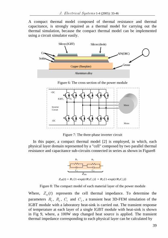
The inverter power module consists of 12 IGBT modules (every arm contained two IGBT modules in parallel to share the current) and each of them paired with an anti-parallel diode. The IGBT has a chip area of 133 mm2 (13.7mm×9.7mm) per one chip and the diode has a chip area of 41mm2 (6.4mm×6.4mm) per one chip, they are separated by 6mm. The rating of the IGBTs and diodes is 850V/200A. The circuit connection is shown in Figure7.
A cross sectional view of each single IGBT module is shown in Figure6. Silicon IGBT and diode are mounted on the top of an insulative layer, and that is fixed on a base-plate, the IGBT module is mounted on a laboratory heat-sink.
J. Electrical Systems 1-4 (2005): 33-46
39
A compact thermal model composed of thermal resistance and thermal capacitance, is strongly required as a thermal model for carrying out the thermal simulation, because the compact thermal model can be implemented using a circuit simulator easily.
Copper (Baseplate)
Aluminium alloy
Silicon (IGBT) Silicon (diode)
Cu
Solder AIN(DBC)
Grease
Figure 6: The cross section of the power module
Inverter Circuit
+DC
-DC Motor
IGBT1 D1
Motor
Figure 7: The three-phase inverter circuit
In this paper, a compact thermal model [2] is employed, in which, each physical layer domain represented by a "cell" composed by two parallel thermal resistance and capacitance sub-circuits connected in series as shown in Figure8
R1 R2
C1 C2
Zthi
Zth(t) = R1{1-exp(t/R1C1)} + R2{1-exp(t/R2C2)}
Figure 8: The compact model of each material layer of the power module
Where, ( )thZ t represents the cell thermal impedance. To determine the parameters 1R , 2R , 1C and 2C , a transient heat 3D-FEM simulation of the IGBT module with a laboratory heat-sink is carried out. The transient response of temperature at each layer of a single IGBT module with heat-sink is shown in Fig 9, where, a 100W step changed heat source is applied. The transient thermal impedance corresponding to each physical layer can be calculated by

Z. Zhou et al: Loss Calculation and Thermal Modelling for 3 Phase Inverter...
40
( 1)( ) ( ( ) ( )) /thi thi th i cZ t T t T t P−= − (13)
where, ( )iT t represents the temeprature at the thi layer of the module (i=0, 2,…10); cP is the heat source applied in the 3D-FEM simulation. The transient thermal impedance corresponding to each physical layer is shown in Figure 10.
Figure 9: Step resonse of temperature at each layer of the power module (FEM)
Figure 10: Eqivalent thermal impedance for each layer of the compact model
By using a curve fitting approach, the parameters 1R , 2R , 1C and 2C can be extracted for each layer. So the compact IGBT thermal model can be
10-4
10-3
10-2
10-1
100
101
102
103
104
105
0
0.02
0.04
0.06
0.08
0.1
0.12
Time (sec.)
Equ
ival
ent t
herm
al im
peda
nce
of e
ach
laye
r (K
/W)
zf1zf2zf3zf4zf5zf6zf7zf8zf9
10-4
10-3
10-2
10-1
100
101
102
103
104
105
35
40
45
50
55
60
Time (sec.)
Tem
pera
ture
of e
ach
laye
r (D
dgre
e C
) ( R
C n
etw
ork)
T1T2T3T4T5T6T7T8T9

J. Electrical Systems 1-4 (2005): 33-46
41
represented by a number of series connected cells, and each cell of the thermal network can correspond to a physical layer of the IGBT module from the layer temperature point of view.
For a multi-IGBT modules mounted on a common heat-sink system, the thermal model considering thermal interference among chips can be expressed as
1 111 12 1
2 21 22 2 2
1 2
j Lm
j m L
m m mm Lmjm
T PZ Z ZT Z Z Z P
Z Z Z PT
⎡ ⎤ ⋅ ⋅ ⋅ ⋅ ⎡ ⎤⎡ ⎤⎢ ⎥ ⎢ ⎥⎢ ⎥⋅ ⋅ ⋅ ⋅⎢ ⎥ ⎢ ⎥⎢ ⎥= ⋅⎢ ⎥ ⎢ ⎥⎢ ⎥⋅ ⋅ ⋅ ⋅ ⋅ ⋅ ⋅ ⋅⋅⎢ ⎥ ⎢ ⎥⎢ ⎥⋅ ⋅ ⋅ ⋅⎢ ⎥ ⎣ ⎦ ⎣ ⎦⎣ ⎦
(14)
where the diagonal elements ( i j= ) correspond to the self-impedance of each chip, whereas off-diagonal elements ( i j≠ ) are mutual-impedances. LiP , jiT ( 1, 2...i m= ) represent m heat sources and junction temepratures. As visible in Figure 7, the number of the heat sources is 24m = . The elements in EQ. (11) can determined by a 3-D numerical simulation. For the purpose of illustrating the power loss and thermal simulation approach proposed in this paper, a relative simple thermal model is utilised, in which, considering the sufficient distance between the adjacent chips (more than 6mm), the thermal interference of the heat flux from different heat sources along the layers of IGBT module is relative small as shown in Figures 11-14 and is ignored in this paper.
Therefore, the elements ( )ij bhsZ i j Z≠ = . All the self-impedances ( )ijZ i j= can be determined by the 3D-FEM simulation in Figure9-10. The proposed thermal model has the capability to represent the interference of the heat flux from different heat sources that are adjacent to each other. Specifically, the interference of the heat flux can be represented by merging the individual thermal models at individual points where the different heat fluxes interfere with each other. The bottom of heat-sink represented by bhsZ is chosen as the fully thermal interference part in the compact thermal model.
The corresponding equivalent thermal network of the inverter power module and heat-sink is shown in Figure 15, where aT =50oC.
Where, the thermal parameters of the bottom heat-sink are chosen by reference a Semikron water-cooled heat-sink thermal model (SKiiPPACK 3, 6 liter/ min flow rate), and employed in the simulation. The parameters are given in the table-1 and table-2 [10].

Z. Zhou et al: Loss Calculation and Thermal Modelling for 3 Phase Inverter...
42
IGBT
Diode Aluminium plate
Base plate
Figure 11: a 2 in 1 IGBT 3D model simulation module.
Figure 12: Heat transfer along cross section of the IGBT module with a single heat
source (100W).
Figure 13: Surface temperature of the IGBT module with a single heat source (100W).
Figure 14: Surface temperature of the IGBT module with two heat sources (both 100W)

J. Electrical Systems 1-4 (2005): 33-46
43
PL2
PLn
PL1 Tj1
Tj2 Tj1
Tjm
Zbhs
Bottom of heat-sink
Tbhs Ta
Figure 15: Eqivalent thermal network of the inverter power module and heat-sink.
Table.1: Thermal resistance
1R (K/W) 2R (K/W) 3R (K/W) 4R (K/W) 2.143×10⁻³ 3.818×10⁻³ 9.045×10⁻³ 2.535×10⁻³
Table. 2: Time constant
1t (s) 2t (s) 3t (s) 4t (s) 2.204×10⁻¹ 2.911 2.0×101 1.355×10²
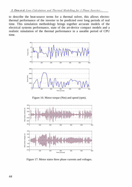
5. SIMULATION RESULTS
Simulation program is developed in Matlab/Simulink. Simulation of the power losses and thermal performance for the inverter drive system shown in Figure7 is carried out. The specified torque and speed profiles are shown in Figure 16, the corresponding continuous effective motor stator currents and voltage are shown in Figure17, The power losses in IGBT1 and diode D1 and the corresponding junction temperature are shown in Fig18-19 respectively. The temperature of inlet water is set to 50°C.
The PWM switching frequency is set to 2 kHz, and simulation time step is 0.5ms. The total simulation time takes about 1hr with a 3.12 GHz CPU, 1Gbyte memory PC.
6. CONCLUSIONS A fast power losses simulation model for a three-phase inverter power module (IPM) thermal simulation using PWM reconstruction technique is proposed in this paper. In this model, an inverter drive system simulation model with the aim of fast and efficient power loss and thermal analysis for inverter power devices in electrical vehicle applications. This approach has a very fast simulation speed and produces the voltages and currents associated with each of the semiconductor switches in real-time by using PWM reconstruction. This information is then used in conjunction with detailed device switching models,
Z. Zhou et al: Loss Calculation and Thermal Modelling for 3 Phase Inverter...
44
to describe the heat-source terms for a thermal solver, this allows electro-thermal performance of the inverter to be predicted over long periods of real time. This simulation methodology brings together accurate models of the electrical systems performance, state of the art-device compact models and a realistic simulation of the thermal performance in a useable period of CPU time.
Figure 16: Motor torque (Nm) and speed (rpm).
Figure 17: Motor stator three phase currents and voltages.
0 100 200 300 400 500 600-300
-200
-100
0
100
200
300
Mot
or p
hase
cur
rent
s (A
)
0 100 200 300 400 500 600-150
-100
-50
0
50
100
150
Time (second)
Mot
or p
hase
vol
tage
s (V
)
0 100 200 300 400 500 600-100
-50
0
50
100
Torq
ue (N
m)
0 100 200 300 400 500 6000
1000
2000
3000
4000
Time (second)
Spe
ed (r
pm)

J. Electrical Systems 1-4 (2005): 33-46
45
Figure 18: power losses of IGBT (W).
Figure 19: Junction temperature of IGBT (oC).

Z. Zhou et al: Loss Calculation and Thermal Modelling for 3 Phase Inverter...
46
Acknowledgment
The authors would like to thank Toyota Motor Corporation for their financial support and technical advice.
REFERENCES
[1] M. Ishiko, M. Usui, T. Ohuchi and M. Shirai, Design Concept for Wire- Bonding Reliability Improvement by Optimizing Position in Power Devices, ISPS’04 7th International Conference on Power Semiconductors, Prague, 31 August – 3 September 2004, pp 39 44, 2004.
[2] T. Kojima, Y. Yamada, M. Ciappa, M. Chiavarini and W. Fichtner, A Novel Electro-thermal Simulation Approach of Power IGBT modules for automotive traction applications, Proceeding of 2004 international symposium on power semiconductor devices & ICs, Kitakyushu, 2004.
[3] H. A. Mantooth and A. R. Hefner, Electrothermal Simulation of an IGBT PWM inverter, IEEE Transaction on Power Electronics, vol. 12, no.3, May 1997.
[4] R. Hefner and D. L. Blackburn, Thermal component models for electro-thermal network simulation, IEEE Transactions on Components Package. Manufacture. Technology, vol. 17, p. 413, 1994.
[5] A. D. Rajapakse, A. M. Gole, and P. L. Wilson, Electromagnetic Transient Simulation Models for Accurate Representation of Switching Losses and Thermal Performance in Power Electronic Systems, IEEE Transactions on Power Delivery, vol.20, no.1, pp 319-327, 2005.
[6] D. Xu, H. Lu, L. Hang, S. Azuma, M. Kimata and R. Uchida, Power Loss and Junction Temperature Analysis of Power Semiconductor Devices, IEEE Transaction on Industry Applications, Vol..38, No.5, pp, 1426-1431, September/October 2002.
[7] Introduction to the 600V ADD-A-pak TM and INT-A-pakTM IGBT Modules, International Rectifier Application notes 1992.
[8] A. Laprade and R. H. Randal, Numerical Method for Evaluating IGBT Losses, Application Note 7520 Rev. A1.
[9] Analog Devices: ADMC401 Double Update Mode of PWM generation Unit, Analog Devices, Inc., 1999.
[10] Semikron application notes on heat sink systems.