new approach of constructing adpll by a novel quadrature ...iaiest.com/dl/journals/7- iaj of science...
TRANSCRIPT
International Academic
Journal of
Science
and
Engineering International Academic Journal of Science and Engineering Vol. 3, No. 4, 2016, pp. 44-60.
ISSN 2454-3896
44
www.iaiest.com
International Academic Institute for Science and Technology
New approach of constructing ADPLL by a novel Quadrature
Ring Oscillator using Low-Q Series LC tanks
Marzieh Chaharboor
a, Saman Mokhtabad
b, Hojat Ghonoodi
c
aM.Sc Electrical and Electronic Engineering, Hadaf Institute of Higher Education, Sari, Iran.
bM.Sc Electrical and Electronic Engineering, Hadaf Institute of Higher Education, Sari, Iran.
cPhD Electrical and Electronic Engineering, Noshirvani University of Technology,Babol, Iran.
Abstract
Nowadays, the All-Digital Phase-Locked Loop (ADPLL) as a digital electronic circuit is applied in
modern communication systems. The main components of ADPLL such as phase detector, loop filter and
voltage controlled oscillator which are all digitally discussed in detail. On the other hand, sensitivity to
parasitic mismatches in LC oscillators and the limitation of the robustness and the quantization noise
cause trying to overcome these challenges by a VCO and also a delta-sigma digital to analog converter
which are essential for this aim. A new quadrature oscillator topology which includes four low-Q series
LC tanks in a ring structure is employed in this paper. In the following, low distortion delta-sigma MASH
architecture includes the advantages and significant specifications to achieve better performance, is
explained. The proposed idea relying on studies of ADPLL efforts unlike the most of the previous works
uses a ring oscillator. With quadrature ring structure, an ideal condition of implementation is provided
that keeps all the advantages of previous works and even better off. To confirm and evaluate the analysis,
the proposed structure simulated using TSMC 0.18μm model technology. The results confirm the
proposed idea of implementation and higher performance of this structure.
Keywords: All-Digital Phase Locked Loop (ADPLL), Digitally Controlled Oscillator (DCO),
Complementary Metal Oxide Semiconductor (CMOS), Quadrature Inverter Based Ring Oscillator, Series
LC tank, Low-Distortion Delta-Sigma Mash topology, Low phase noise, Low Quantization Noise

International Academic Journal of Science and Engineering,
Vol. 3, No. 4, pp. 44-60.
45
Introduction:
In the last decade, the DCO structure in order to achieve high performances for All-Digital Phase Locked
Loop (ADPLL) which is used in various communication devices has been introduced (Jalil, J et al, 2014).
A DCO produces a stable digital frequency with smooth tuning in both DPLL and ADPLL and it is
correspond to voltage controlled oscillator (VCO) of analog PLL. Typically, the frequency of DCO is
tuned by varactors. Design of DCO by LC oscillators suffers from some kinds of challenges, such as
limited robustness, mismatches, poor linearity; high circuit complexity and high power consumption
(Chan, C. and Choy, O., 2001). Staszewski et al (Staszewski et al, 2005) introduced a solution that
achieved to the desired DCO frequency resolution but in any ΔΣ data converter, the quantization noise is
moved to higher frequencies where the phase noise specifications are more challenging (Fanori, L et al,
2010). Another solution is using a delta- sigma digital to analog converter and a VCO to overcome these
challenges so the controlled oscillator is a key component in PLLs. In majority of previous works an LC
oscillator is used because of better phase noise performance than ring oscillator. In this paper a new
structure of quadrature ring oscillator is considered. The proposed implementation including a ∆Σ DAC
and analog filter for inputs of the applied analog quadrature oscillator which using low-Q series LC tanks.
With applying this oscillator wide tuning range and better phase noise are provided while it occupies
small area. With the improvement of quantization level, phase noise, power consumption, decreasing the
unwanted parameters will occur and cause to all-digital phase locked loop have become more precious.
The organization of this paper is as follows: In All-Digital phase locked loop, the components of PLLs
and different types of PLLs are described and the ADPLL is investigated. In DCO and VCO, the
corresponding and the relation between them are described and how a VCO could play a critical role in
ADPLL to overcome the challenges of DCO’s operations explained properly. In Sketch of applied VCO,
a considered quadrature oscillator with new topology of inverter based ring structure is detailed. The
Low-Distortion Delta-Sigma MASH Topology is about the advantages of this topology over traditional
and how to reach a low noise in digital conversions and higher performance. The proposed idea of
implementation and the improvements is presented in Idea of the Implementation. In Simulation Results,
to confirm the idea a quadrature oscillator (QO) base on considered ring configuration simulated by using
the practical 0.18 μm TSMC CMOS technology and the results show the agreements.
All-Digital Phase Locked Loop (ADPLL):
Outlines of PLLs
The Phase-Locked Loop (PLL) is an important and extremely versatile circuit, used in electronic
communication systems like frequency generator and frequency synthesizer and modulator. Phase Locked
Loop (PLL) is an electronic feedback circuit which Locks an output signal phase relative to input
reference signal. The input signal may be any periodic waveform such as sinusoidal or digital clock (Best,
R, 2003), (Bizzarri, F, 2012). A PLL has three operating states: free running, capture and lock. In free
running state, the feedback loop is open and there is no external input frequency, the VCO oscillates at
the natural frequency. In captured state an external input signal is necessary and feedback loop should be
completed. The PLL is in process of acquiring frequency lock in the capture state. In Lock state, the
output frequency of VCO is locked onto the frequency of external input signal (Deepika Ghai and Neelu
Jain, 2013). There are three main building blocks of PLL: Phase detector (PD) or phase/frequency
International Academic Journal of Science and Engineering,
Vol. 3, No. 4, pp. 44-60.
46
detector (PFD), Loop Filter, Voltage Controlled Oscillator (VCO). PLLs are classified into various
categories: Analog or linear PLL, Digital PLL, ALL Digital PLL (Prasad, V. and Sharma, D. C, 2012). In
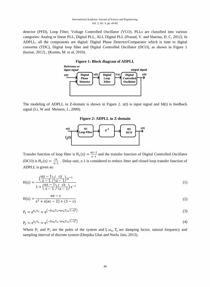
ADPLL, all the components are digital: Digital Phase Detector/Comparator which is time to digital
converter (TDC), Digital loop filter and Digital Controlled Oscillator (DCO), as shown in Figure 1
(kumar, 2012) , (Kumm, M. et al, 2010).
Figure 1: Block diagram of ADPLL
The modeling of ADPLL in Z-domain is shown in Figure 2. x(t) is input signal and fd(t) is feedback
signal (Li, W and Meiners, J., 2000).
Figure 2: ADPLL in Z-domain
Transfer function of loop filter is ( )
and the transfer function of Digital Controlled Oscillator
(DCO) is ( )
. Delay unit, z-1 is considered to reduce Jitter and closed loop transfer function of
ADPLL is given as:
( ) (
) (
)
(
) (
) (1)
( )
( ) ( ) (2)
(
√ ) (3)
(
√ ) (4)
Where P1 and P2 are the poles of the system and are damping factor, natural frequency and
sampling interval of discrete system (Deepika Ghai and Neelu Jain, 2013).
International Academic Journal of Science and Engineering,
Vol. 3, No. 4, pp. 44-60.
47
( ) * ( √
)+ (5)
(6)
Where C1 and C2 are the coefficients of characteristics equation.
Parameters of ADPLL
The important parameters of ADPLL are as follows:
(a) Stability of ADPLL system: ADPLL system must be stable if all poles of characteristics equation lie
within the unit circle.
(b) Steady state error of ADPLL system: Errors may be caused due to phase and frequency.
(c) Phase error: when phase and the frequency of input signal is unit step, the phase and the frequency
error of the ADPLL is eliminated by close loop system (Deepika Ghai and Neelu Jain, 2013).
(d) If noise is present in the input signal, then output suffers from noise (Hajimiri, A., 2001).
Characteristics of PLL noise at input is similar to low pass filter. Increasing the bandwidth of PLL could
be one way to reduce the noise at the output of VCO.
(e) Jitter Reduction: Jitter is term variation of signal w.r.t (waveform relative to time) to its ideal position
in time. Clock jitter is a parameter which affects the system performance. Output signal will experience
jitter because of internal circuitry, additive noise in circuit and parasitic element. Clock recovery circuit
takes the clock from the noisy data (Fahim, A.M., 2003). One way to reduce noise is narrow loop
bandwidth that effect of jitter on clock can be minimized by it.
(f) Power consumption: In ADPLL, charge pump, current generators, voltage to current converters are not
used, therefore power consumption reduces up to 15% (Deepika Ghai and Neelu Jain, 2013).
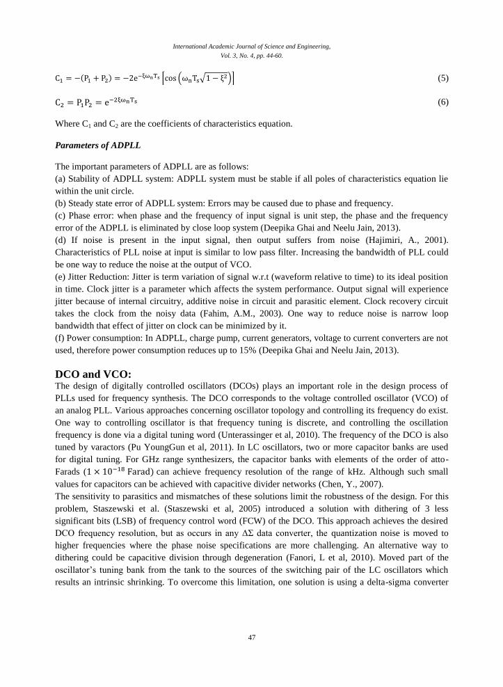
DCO and VCO: The design of digitally controlled oscillators (DCOs) plays an important role in the design process of
PLLs used for frequency synthesis. The DCO corresponds to the voltage controlled oscillator (VCO) of
an analog PLL. Various approaches concerning oscillator topology and controlling its frequency do exist.
One way to controlling oscillator is that frequency tuning is discrete, and controlling the oscillation
frequency is done via a digital tuning word (Unterassinger et al, 2010). The frequency of the DCO is also
tuned by varactors (Pu YoungGun et al, 2011). In LC oscillators, two or more capacitor banks are used
for digital tuning. For GHz range synthesizers, the capacitor banks with elements of the order of atto-
Farads ( ) can achieve frequency resolution of the range of kHz. Although such small
values for capacitors can be achieved with capacitive divider networks (Chen, Y., 2007).
The sensitivity to parasitics and mismatches of these solutions limit the robustness of the design. For this
problem, Staszewski et al. (Staszewski et al, 2005) introduced a solution with dithering of 3 less
significant bits (LSB) of frequency control word (FCW) of the DCO. This approach achieves the desired
DCO frequency resolution, but as occurs in any ΔΣ data converter, the quantization noise is moved to
higher frequencies where the phase noise specifications are more challenging. An alternative way to
dithering could be capacitive division through degeneration (Fanori, L et al, 2010). Moved part of the
oscillator’s tuning bank from the tank to the sources of the switching pair of the LC oscillators which
results an intrinsic shrinking. To overcome this limitation, one solution is using a delta-sigma converter

International Academic Journal of Science and Engineering,
Vol. 3, No. 4, pp. 44-60.
48
and a VCO instead of large array of MOSCAP devices for capacitor banks. This method allows an easier
design without any additional drawbacks on the phase noise performance. In this work a new topology
for digitally controlled oscillator (DCO) is considered based on Figure 3, the loop including ΔΣ DAC, a
low pass filter and an analog oscillator. A characteristic of the DCO is so important to be developed
specially for frequency tuning.
Figure 3: direct digital synthesis of digitally controlled oscillator
In previous works, typically an LC oscillator is used because of its better phase noise performance than
ring oscillators but in this work a new topology of ring oscillator is considered with a good phase noise
and wide tuning range while it could occupy small area. In the following the details of employed topology
are described.
Sketch of applied Voltage Controlled Oscillator: Generally the main aim of VCOs that are designed is minimizing the phase noise. They should have
desirable DC power dissipation, tuning range, the output voltage swing and die are. In previous works
most LC-VCO has been a better choice than ring oscillators. However ring topologies have some
advantages like the output signals with different phases. A Tiny quadrature oscillator is employed in this
work that four low-Q series LC tanks are in a ring structure driven by inverters operating in class D. It
occupies the small area in comparing with previous ring oscillators while significantly reducing the phase
noise and maintaining wide tuning range (Tohidian, M et al, 2015). The tank’s output voltage is amplified
QLC times and shifted -90 at the resonant frequency f0. To work properly, the tank should be driven by a
low impedance source and its output should be seen by high impedance. A simple CMOS inverter, as
shown in Figure 4 driven by a sufficiently large input signal will provide such low driving impedance
while acting as a high-impedance isolator to preceding stage. Since the inverter input is sinusoidal, it’s
output jumps rapidly between two supply rail voltages, 0V and VDD, thus producing a near square wave
(Tohidian, M et al, 2015).
Figure 4: Class-D amplifier as a low output impedance divider
International Academic Journal of Science and Engineering,
Vol. 3, No. 4, pp. 44-60.
49
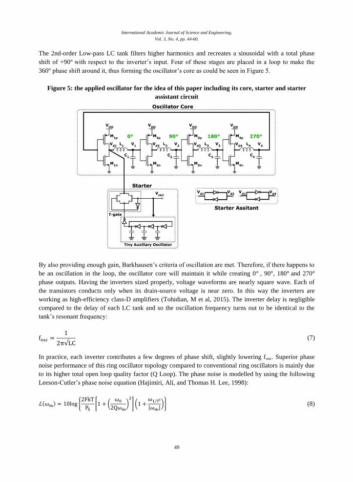
The 2nd-order Low-pass LC tank filters higher harmonics and recreates a sinusoidal with a total phase
shift of +90 with respect to the inverter’s input. Four of these stages are placed in a loop to make the
360 phase shift around it, thus forming the oscillator’s core as could be seen in Figure 5.
Figure 5: the applied oscillator for the idea of this paper including its core, starter and starter
assistant circuit
By also providing enough gain, Barkhausen’s criteria of oscillation are met. Therefore, if there happens to
be an oscillation in the loop, the oscillator core will maintain it while creating 0 , 90 , 180 and 270
phase outputs. Having the inverters sized properly, voltage waveforms are nearly square wave. Each of
the transistors conducts only when its drain-source voltage is near zero. In this way the inverters are
working as high-efficiency class-D amplifiers (Tohidian, M et al, 2015). The inverter delay is negligible
compared to the delay of each LC tank and so the oscillation frequency turns out to be identical to the
tank’s resonant frequency:
(7)
In practice, each inverter contributes a few degrees of phase shift, slightly lowering fosc. Superior phase
noise performance of this ring oscillator topology compared to conventional ring oscillators is mainly due
to its higher total open loop quality factor (Q Loop). The phase noise is modelled by using the following
Leeson-Cutler’s phase noise equation (Hajimiri, Ali, and Thomas H. Lee, 1998):
( ) {
[ (
)
] ( ⁄
| |)} (8)

International Academic Journal of Science and Engineering,
Vol. 3, No. 4, pp. 44-60.
50
Where:
K-Boltzmann constant;
T-absolute temperature;
Ps-average power dissipated in the resistive part of tank;
0-oscillation frequency;
Q-quality factor (also known as loaded Q);
–offset from the carrier;
–corner frequency between 1/f3 and 1/f
2 zones of the noise spectrum;
F- Empirical parameter, called excess noise factor;
As calculated in (Razavi, B., 1996) QLoop of a 4-stage inverter ring oscillator is 1.4. Applying the same
methodology, QLoop of the considered oscillator is 4 QLC.
Therefore, a very poor quality LC tank, even as low as 1.5(due to its tiny size) makes the total QLoop
6,thus substantially improving its phase noise. Due to the Low quality of LC tanks, phase noise sensitivity
to mismatches is very low and even a few percent capacitor mismatch doesn’t degrade phase noise
noticeably and only introduces a few degree of I/Q phase error.
In (Savoj, J. and Razavi, B., 2003) a multiphase ring structure uses parallel LC tanks. Consequently it
oscillates at a lower frequency than the tank’s resonance with 45 phase shift per LC stage.
This reduces QLoop from the maximum possible. A similar structure is also used in (Rogers, J. E. and
Long, J. R., 2002) with four delay lines in a loop. However, the use of low-efficiency differential
amplifiers has been resulted in poor phase noise. Oscillation amplitude of the considered oscillator can be
calculated for each stage.
Oscillation amplitude for one stage
The amplifier as a voltage-controlled limiting voltage source of output resistance Rout switching between
the ground (0) and VDD. Signal Vd is then approximated with an ideal square waveform, and signal Vd,sq,
with amplitude Ad. The first harmonic of Vd,sq is
times of Ad and so output voltage amplitude becomes:
Aout=
Ad QLC (9)
From (9), peak current of the tank, that is sinusoidal and out of phase with Vin, is derived:
Ipeak=
.
=
(10)
At the peak of input voltage, where NMOS is in deep triode, Vd reaches
. Using MOS current
equation in triode and (9):
Id=K(Vgs –Vth)Vds = K (Ain+
-Vth) (
-
.
) (11)
Where K is the transistor strength equal to n Cox (
).

International Academic Journal of Science and Engineering,
Vol. 3, No. 4, pp. 44-60.
51
At a steady-state oscillation, Ain must be equal to Aout. Also, considering that NMOS current in (11) is the
same as tank peak current in (10), so the oscillation amplitude can be found. The oscillation amplitude is
calculated versus transistor size. The wider transistor, the lower output resistance of the inverter and
consequently higher amplitude. For weaker transistors, the drain current deviates from (11) towards lower
values and the loop might not even have enough gain for oscillation (Tohidian, M et al, 2015).
Start UP circuit
Before the oscillation could begin, the devices would normally be biased at proper dc operating points.
Intrinsic device noise may find a small-signal loop gain higher than unity with 360 phase shift at a
certain frequency, so that the oscillation could be buildup (Tohidian, M et al, 2015). Contrarily, in the
considered oscillator core, even though oscillation amplitude can be found in which the loop has a large
signal gain of unity or more, it will never start oscillation on its own. Since the core contains four
inverting amplifiers, there is a strong positive feedback in the loop at dc (with shorted inductors and
opened capacitors) that forces the outputs of inverters to get stuck at 0 and VDD (Vd1=Vd3=0 and
Vd2=Vd4=VDD). At this state, the oscillator core is locked and gain of inverter is almost zero, thus no
oscillation will occur (Tohidian, M et al, 2015).
Consequently, a starter circuit is added (as shown in Figure 5) to directly put the core in a large-signal
mode, thus initiating the oscillation. The starter consists of a simple under-sized auxiliary ring oscillator,
and a T-gate switch that connects it to the core. At first, the auxiliary oscillator is turned on and connected
to Vd1 .It makes periodical perturbations to Vd1 at close to the fosc rate. Large enough perturbations can
pull the second stage out of the dc lock state, which is then propagated to all stages. After oscillation is
established in the main core (in few Nano-seconds), the auxiliary oscillator is turned off and
disconnected. This operation is similar to starting a car engine using its starter.
It could be shown that in the large-signal mode the total loop dc gain drops to less than unity and
therefore the oscillator cannot fall back into the lock state .As shown in Figure 5, adding back-to-back
inverters between the complementary outputs (i.e., ⁄ ) assists with the start up. Three dummy T-
gates in off state connected to outputs of the core inverters are also used to balance core phases (Tohidian,
M et al, 2015). The described oscillator in ring structure consists of four stages with in-phase and
quadrature output signals. The quadrature signals are suitable because the division by two is done and
also the oscillator may run at half the frequency, too. There are different ways to generate quadrature
signals and even-stage ring oscillators can be addressed between them (Ghonoodi,H. and Miar Naimi,H. ,
2012). In previous works, although ring oscillators have capability of generating quadrature outputs but
because they suffer from poor phase noise, they have been ignored (Naimi, H., and Ghonoodi, H, 2010).
In this work a new topology of quadrature ring structure has been used in ADPLL. On the other hand, a
quadrature oscillator itself acts as a self-phase-error correcting. A quadrature oscillator also uses a PLL-
loop and exact quadrature signals are indispensable for direct conversion, especially this direct conversion
is a main goal of RF receivers (Ghonoodi,H. and Miar Naimi,H. , 2012). In addition to the low in-band
phase noise and high linearity imposed by the IEEE 802.11a wireless LAN (WLAN) standard, Very
accurate quadrature matching is required to minimize the number of incorrectly received bits (Come, B. et
al, 2000). Most of the previously reported WLAN RFICs are designed to work with a certain companion
digital baseband chip and quadrature outputs test signal and give information to control a code and also a

International Academic Journal of Science and Engineering,
Vol. 3, No. 4, pp. 44-60.
52
quadrature oscillator acts with auto-calibration and auto tuning mechanism (Ghonoodi,H. and Miar
Naimi,H. , 2012). So, in this paper, a quadrature ring structure oscillator with improved phase noise
considered as a VCO for implementation of an ADPLL.
Low-Distortion Delta-Sigma MASH Topology:
Applied architecture
A low-distortion delta-sigma topology with significant system and circuit-level advantages, over
traditional topologies, especially is using for wideband (low oversampling ratio) applications. This
topology is applied in this paper to achieve higher performance while requiring smaller silicon area and
lower power consumption.
The converters often use multi-stage delta-sigma MASH architectures that operating with low
oversampling ratios (Fujimori, I. et al, 2000), (Vleugels, K. et al, 2001). Delta-sigma data converters rely
on high oversampling ratios to obtain high resolutions and relaxed accuracy requirements for their analog
components. However, at low oversampling ratios, these benefits shouldn’t be taken for granted. High
resolutions can only be obtained by increasing other parameters, such as the noise-shaping or the
quantizer resolution. In addition, distortion components produced by nonlinear opamp gain and limited
slew rate are not adequately attenuated by the delta-sigma loop, so careful opamp design is necessary to
avoid those effects. One way to deal with the issue of opamp distortion is prevent the op-amps from
processing input signal. This can be achieved by making the modulator’s signal transfer function (STF)
equal to 1 which allows for input signal and the quantization noise to be processed separately (Benabes .P
et al,1993), (J. Steensgaard,1999), (Silva, J. et al, 2001). This technique has advantages and is especially
useful for MASH architectures.
Theory of low-distortion operation
Figure 6 shows a generic L-order cascade-of-integrators feedforward (CIFF) topology, as described in
(Mathworks.com). Consider the case when b1=b2=…=bL-1=0 and b0=bL=1. It can be easily verified that in
this case, STF (z) =1. For this condition, the input signal u is cancelled in e and the integrators process
quantization noise only. Therefore, their nonlinearities do not affect the transmission of the input signal u.
This concept can be applied to noise-shaping of any order or complexity (Hamoui, A. and Martin, K.
2002).
Figure 6: Generic L-Order feedforward topology

International Academic Journal of Science and Engineering,
Vol. 3, No. 4, pp. 44-60.
53
A particular case is the second-order topology shown in Figure 7. Its main features are feedforward path
and the absence of DAC signal feedback to the second integrator (Silva, J. et al, 2001).
Figure 7: Low-Distortion second-order topology
Advantages of the Low-Distortion Topology:
In addition to reduce sensitivity to opamp nonlinearities, the low-distortion topology has the following
advantages:
Lower area and power consumption in multibit implementations
Since the integrators process quantization noise only, their coefficients can be scaled according to the
quantizer resolution (N). Integrator coefficients are optimum for maximum opamp output swing under
ideal conditions. The integrator coefficients can be larger than a traditional topology. Hence, for the same
sampling capacitor sizes, the coefficients constrained by KT/C noise consideration, the integrating
capacitors can be smaller, resulting in area saving.
When designing the opamps, the bias currents are determined from bandwidth or slew rate requirements.
The power consumption is proportional to SR.CL, where SR and CL are the slew rate and load capacitance
of each opamp respectively. Depending on the choice of coefficients and targeted OSR, considerably
lower power consumptions can be achieved. In practice, there are reasons to make the integrator
coefficients somewhat smaller. The opamp outputs include not only quantization noise, but also noise
caused by circuit non-idealities (DAC errors, KT/C noise) (Silva, J. et al, 2001).
They may also include dither. If opamp bandwidth is an issue, the coefficient values can be lowered to
increase the feedback factors and therefore reduce the unity-gain bandwidth requirements. Opamp slew-
rate requirements can also be reduced. Also, it may be desirable to use less of the available dynamic range
to reduce distortion. Although opamp distortion does not affect the input signal u, it will modulate
quantization noise and may reduce the maximum achievable SNR (Silva, J. et al, 2001).
Improved input signal range
The output swing of the opamps does not limit the input signal amplitude. In fact, the only elements that
have to accommodate the full input signal swing are the switches and the quantizer. In traditional
topologies, care must be taken to ensure that the opamp outputs do not saturate for the maximum signal
amplitude, which is accomplished by designing the integrator coefficients for the worst case. This is not
necessary in the low-distortion topology (Silva, J. et al, 2001).
International Academic Journal of Science and Engineering,
Vol. 3, No. 4, pp. 44-60.
54
Only one DAC in feedback path
Most delta-sigma A/D modulator topologies use distributed feedback and require two or more DACs in
their implementation. Although not necessary for low-distortion operation, the considered topology has
only one DAC in feedback loop, making it more convenient for circuit implementation. For multibit
DACs, the saving in term of area and complexity can be significant, especially if calibration is used for
DAC linearization (Silva, J. et al, 2001).
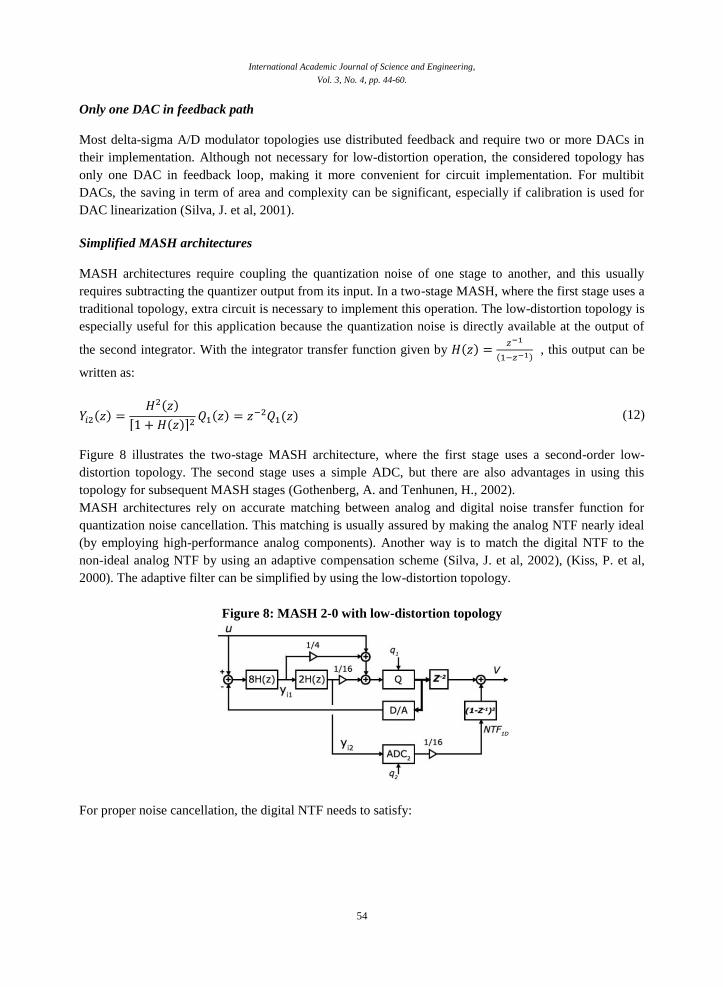
Simplified MASH architectures
MASH architectures require coupling the quantization noise of one stage to another, and this usually
requires subtracting the quantizer output from its input. In a two-stage MASH, where the first stage uses a
traditional topology, extra circuit is necessary to implement this operation. The low-distortion topology is
especially useful for this application because the quantization noise is directly available at the output of
the second integrator. With the integrator transfer function given by ( )
( ) , this output can be
written as:
( ) ( )
[ ( )] ( )
( ) (12)
Figure 8 illustrates the two-stage MASH architecture, where the first stage uses a second-order low-
distortion topology. The second stage uses a simple ADC, but there are also advantages in using this
topology for subsequent MASH stages (Gothenberg, A. and Tenhunen, H., 2002).
MASH architectures rely on accurate matching between analog and digital noise transfer function for
quantization noise cancellation. This matching is usually assured by making the analog NTF nearly ideal
(by employing high-performance analog components). Another way is to match the digital NTF to the
non-ideal analog NTF by using an adaptive compensation scheme (Silva, J. et al, 2002), (Kiss, P. et al,
2000). The adaptive filter can be simplified by using the low-distortion topology.
Figure 8: MASH 2-0 with low-distortion topology
For proper noise cancellation, the digital NTF needs to satisfy:
International Academic Journal of Science and Engineering,
Vol. 3, No. 4, pp. 44-60.
55
( )
( ) ( ) ( )
( ) (13)
Where n0, n1 and n2 are correction terms that compensate for circuit imperfections such as opamp finite
gain and capacitor mismatch errors. To have a same result with equation (13), a traditional MASH
architecture requires:
( )
[ ( )] ( ) ( )
( )
(14)
Note that coefficients d1, d2 and d3 are necessary for compensating circuit imperfections. Hence equation
(14) needs to be implemented as an IIR filter, or approximated by a high-order FIR filter. Equation (13)
requires only a 3-tap FIR filter, and therefore the traditional architecture is simpler to implement (Silva, J.
et al, 2001). In the applied structure, the first stage is implemented by low-distortion modulator. It uses a 5-bit
quantizer in the first stage and a 6-bit quantizer in the second stage. Value of the SNDR versus input
signal amplitude is more desirable than other topologies. On the other hand, the size of capacitors in the
integrators is important for low oversampling ratios. The choice of sampling capacitor size would
generate the total KT/C noise so that is noticeable for better performance. Also the applied structure has
considerable area and power consumption savings for the low-distortion topology. So the lower power
consumption and savings for lower OSR is another advantage of applied topology.
Idea of the Implementation of ADPLL by Quadrature Ring Oscillator
Using Low-Q Series LC Tank: Typically, in many previous works, digital CMOS processes haven’t been provided by desirable and high
quality inductors and also occupy a large area. In different techniques and by different presented circuit
structures, just DCO’s wide tuning operation has been improved. The tuning range of an oscillator can be
obtained from:
(15)
Recently, various ring topologies for implementation of DCO have been used. In this work a novel
quadrature ring structure oscillator with four series LC tanks by using tiny inductors with a low-Q and
excellent phase noise is considered to achieve a wide tuning range operation with a fine delay like LC
oscillators. Also optimized power consumption obtained with proposed implementation. Typically, ring
DCOs hardly operate in gigahertz, since digital frequency tuning units normally slow down the oscillation
significantly but here, because the startup circuit has been used to maintain the oscillation condition this
problem is solved. In previous works, the study of submicron CMOS quadrature DCO based on LC
resonator tank shows that it can easily operates in gigahertz frequency range and its phase noise
performance is better than ring in comparison but in this work, because the configuration of ring structure
is different from previous topologies, it could be operating at gigahertz frequency range with series LC
tanks and better noise performance.
International Academic Journal of Science and Engineering,
Vol. 3, No. 4, pp. 44-60.
56
On the other hand, in previous works the combination of digital to analog converter (DAC) and a ring-
based VCO operating in gigahertz range leads to the analog control signal degrade the performance, in
this work with an inverter ring and also applied topology for MASH architecture causes lower phase
noise and also higher performance.
From the study and the analysis of the last advancement in design of DCOs, for this work many efforts
have been done to propose an improved implementation. Since, the inverter delay is negligible compared
to the delay of each LC tank, the oscillation frequency also turns out to be identical to the tank’s resonant
frequency as shown in equation (7).
In addition to the features such as wide tuning range and optimum power, the considered ring DCO is a
suitable choice for designing because it occupies a very small area. The described oscillator in the section
Sketch of applied VCO (Voltage Controlled Oscillator) could also employ Nano scale CMOS transistors
in order to make the total oscillator area as small as possible. The devices like active transistors and
passive elements can be the sources of the noise so applying tiny inductors with a low quality factor (Q)
effect on phase noise. Phase noise is a random deviation in the frequency which can be viewed as a
random variation in zero crossing point depends on considered oscillator; because of quadrature outputs
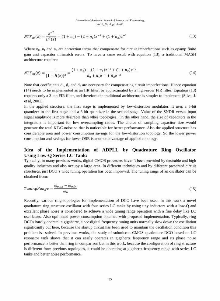
are between 0V and VDD so the phase noise of variation in zero crossing points will not occur. Figure 9
shows the oscillator’s output voltages of first and second stage at the nodes of inverter outputs .
Figure 9: Output Voltages of first and second stage
The power consumption will be optimized by the applied MASH architecture for implementation.
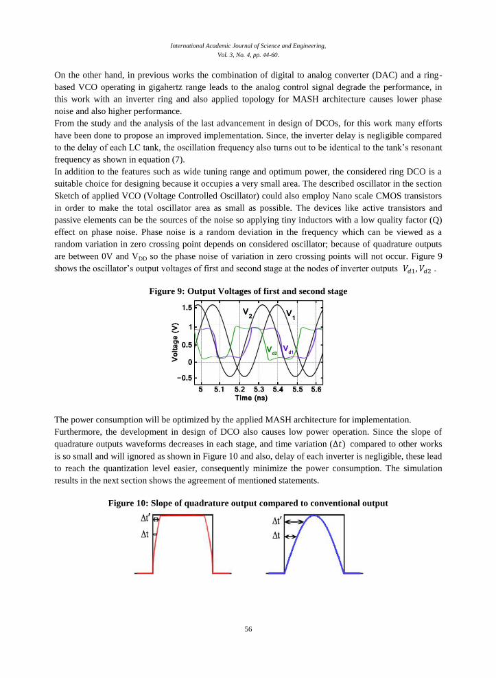
Furthermore, the development in design of DCO also causes low power operation. Since the slope of
quadrature outputs waveforms decreases in each stage, and time variation ( ) compared to other works
is so small and will ignored as shown in Figure 10 and also, delay of each inverter is negligible, these lead
to reach the quantization level easier, consequently minimize the power consumption. The simulation
results in the next section shows the agreement of mentioned statements.
Figure 10: Slope of quadrature output compared to conventional output

International Academic Journal of Science and Engineering,
Vol. 3, No. 4, pp. 44-60.
57
Simulation Results:
In order to verify and approve the Main idea of this paper, the quadrature inverter-based ring oscillator
structure and low-distortion Delta-Sigma MASH architecture simulated with TSMC 0.18µm standard
technology. The Center frequency of oscillator is 2.5GHz. Table 1 is the comparison of conventional RC-
Ring Oscillator and considered quadrature Inverter-based ring oscillator with series LC tanks. As it can be
seen, all the parameters improved by new topology while the transistors scale decreased.
According to the result of simulation that presented in Table 1, the output noise of inverter based ring
oscillator with series LC tank is absolutely lower than the conventional structure. This advantage makes
this oscillator superior topology and improves the quantization of low-distortion delta-sigma MASH
architecture.
Table1- Ring Oscillator Comparison
Conventional
RC-Ring oscillator
Quadrature Inverter based Ring
Oscillator with series LC tank
Center Frequency 2.06GHz 2.5GHz
Capacitor 1.9266pF 6.9pF
Resistor 76.5 ohm -
Inductor - 6.09168nH
Aspect Ratio (W/L) 100µm/0.18µm 40µm/0.18µm
Output Phase Noise
@Freq=1.8GHz 10.5nV @Freq= 1.8GHz 110pV
@Freq=2 GHz 13.5nV (-28dBc) @Freq= 2 GHz 85pV (-300dBc)
@Freq= 2.5GHz 7nV @Freq= 2.5GHz 65pV
Power consumption 1mW 4.7uW
The quantization output of Conventional RC-Ring oscillator and quadrature Inverter-based Ring
Oscillator with series LC tanks are illustrated in Figure 11 and Figure 12 respectively. A good
quantization level is the necessity of ADPLL structure to use in digital and analog RF circuit.
Figure 11: Conventional RC-Ring Oscillator quantized output
International Academic Journal of Science and Engineering,
Vol. 3, No. 4, pp. 44-60.
58
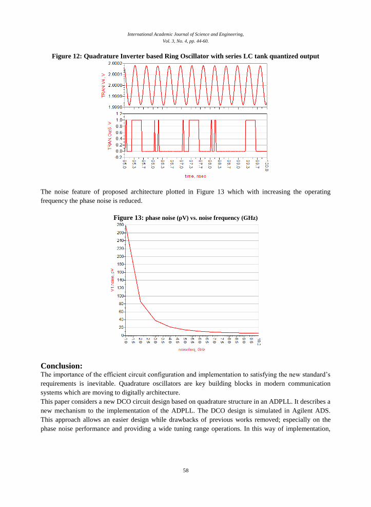
Figure 12: Quadrature Inverter based Ring Oscillator with series LC tank quantized output
The noise feature of proposed architecture plotted in Figure 13 which with increasing the operating
frequency the phase noise is reduced.
Figure 13: phase noise (pV) vs. noise frequency (GHz)
Conclusion: The importance of the efficient circuit configuration and implementation to satisfying the new standard’s
requirements is inevitable. Quadrature oscillators are key building blocks in modern communication
systems which are moving to digitally architecture.
This paper considers a new DCO circuit design based on quadrature structure in an ADPLL. It describes a
new mechanism to the implementation of the ADPLL. The DCO design is simulated in Agilent ADS.
This approach allows an easier design while drawbacks of previous works removed; especially on the
phase noise performance and providing a wide tuning range operations. In this way of implementation,
International Academic Journal of Science and Engineering,
Vol. 3, No. 4, pp. 44-60.
59
the power consumption is optimized. A low- distortion delta-sigma MASH architecture is used to convert
the outputs. The circuit is simulated in a 0.18 m CMOS process. The DCO output features such as low
phase noise and good quantization are shown by simulation results and these results convince that the
proposed structure is desirable for various modern communication applications.
References:
Benabes, P., Gauthier, A., & Billet, D. (1993). New wideband sigma-delta convertor. Electron. Lett.,
29(17), 1575.
Best, R. (2003). Phase-locked loops. New York: McGraw-Hill.
Bizzarri, F., Brambilla, A., & Gajani, G. (2012). Periodic Small Signal Analysis of a Wide Class of Type-
II Phase Locked Loops Through an Exhaustive Variational Model. IEEE Trans. Circuits Syst. I,
59(10), 2221-2231.
Chan, C., and Choy, O. (2001). A low power digital controlled oscillator. International Journal Of
Electronics, 88(4), 463-466.
Chen, Y., Neubauer, V., Liu, Y., Vollenbruch, U., Wicpalek, C., & Mayer, T. et al. (2007). A 9 GHz
dual-mode digitally controlled oscillator for GSM/UMTS transceivers in 65 nm CMOS. 2007
IEEE Asian Solid-State Circuits Conference.
Come, B., Ness, R., Donnay, S., Van der Perre, L., Eberle, W., Wambacq, P., ... & Bolsens, I. (2000).
Impact of front-end non-idealities on bit error rate performance of WLAN-OFDM transceivers.
In Radio and Wireless Conference, 2000. RAWCON 2000. 2000 IEEE (pp. 91-94). IEEE.
Deepika Ghai and Neelu Jain. (2013). "All-Digital Phase Locked Loop (ADPLL) -A Review" -
International Journal of Electronics and Computer Science Engineering-ISSN- 2277-1956.
Fahim, A. M. (2003, September). A compact, low-power low-jitter digital PLL. In Solid-State Circuits
Conference, 2003. ESSCIRC'03. Proceedings of the 29th European (pp. 101-104). IEEE.
Fanori, L., Liscidini, A., & Castello, R. (2010, February). 3.3 GHz DCO with a frequency resolution of
150Hz for All-digital PLL. In Solid-State Circuits Conference Digest of Technical Papers
(ISSCC), 2010 IEEE International(pp. 48-49). IEEE.
Fujimori, I., Longo, L., Hairapetian, A., Seiyama, K., Kosic, S., Jun Cao, & Shu-Lap Chan,. (2000). A
90-dB SNR 2.5-MHz output-rate ADC using cascaded multibit delta-sigma modulation at 8/spl
times/ oversampling ratio. IEEE J. Solid-State Circuits, 35(12),
Ghonoodi, H., and Naimi, H. (2011). A CMOS Quadrature LC Oscillator using Automatic
Phase/Amplitude Calibration. Circuits Syst Signal Process, 31(1), 77-91.
Gothenberg, A., and Tenhunen, H. (2002). Improved cascaded sigma-delta noise shaper architecture with
reduced sensitivity to circuit nonlinearities. Electron. Lett., 38(14), 683.
Hajimiri, A. (2001). Noise in phase-locked loops [invited]. Proceedings of the SSMSD, 1, 1-6.
Hajimiri, A., and Lee, T. (1998). A general theory of phase noise in electrical oscillators. IEEE J. Solid-
State Circuits, 33(2), 179-194.
Hamoui, A. A., and Martin, K. (2002, August). Delta-sigma modulator topologies for high-speed high-
resolution A/D converters. In Circuits and Systems, 2002. MWSCAS-2002. The 2002 45th
Midwest Symposium on(Vol. 1, pp. I-356). IEEE.
Jalil, J., Reaz, M. B. I., Mahalingam, S., Abidin, S. B. Z., & Chang, T. G. (2014). Razvoj digitalno
kontroliranih oscilatora.Tehnicki Vjesnik, 21(4), 897-902.
Kiss, P., Silva, J., Wiesbauer, A., Sun, T., Moon, U. K., Stonick, J. T., & Temes, G. C. (2000). Adaptive
digital correction of analog errors in MASH ADCs. II. Correction using test-signal
injection. Circuits and Systems II: Analog and Digital Signal Processing, IEEE Transactions
on, 47(7), 629-638.

International Academic Journal of Science and Engineering,
Vol. 3, No. 4, pp. 44-60.
60
Kumar, M. (2012). FPGA Implementation of ADPLL with Ripple Reduction Techniques. International
Journal Of VLSI Design & Communication Systems, 3(2), 99-106.
Kumm, M., Klingbeil, H., & Zipf, P. (2010). An FPGA-Based Linear All-Digital Phase-Locked Loop.
IEEE Trans. Circuits Syst. I, 57(9), 2487-2497.
Li, W., and Meiners, J. (2000). Introduction to phase-locked loop system modeling. Analog Applications.
Mathworks.com,. File Exchange - MATLAB Central.
http://www.mathworks.com/matlabcentral/fileexchange.
Naimi, H., and Ghonoodi, H. (2010). Analysis of phase accuracy in CMOS quadrature LC oscillators.
Analog Integrated Circuits And Signal Processing, 67(2), 137-141.
Prasad, V., and Sharma, D. C. (2012). A Review of Phase Locked Loop.International Journal of
Emerging Technology and Advanced Engineering,2(6), 98-104.
Pu, Y. (2011). Low-Power, All Digital Phase-Locked Loop with a Wide-Range, High Resolution TDC.
ETRI J, 33(3), 366-373.
Razavi, B. (1996). A study of phase noise in CMOS oscillators. IEEE J. Solid-State Circuits, 31(3), 331-
343.
Rogers, J., and Long, J. (2002). A 10-Gb/s CDR/DEMUX with LC delay line VCO in 0.18-μm CMOS.
IEEE J. Solid-State Circuits, 37(12), 1781-1789.
Savoj, J., and Razavi, B. (2003). A 10-Gb/s CMOS clock and data recovery circuit with a half-rate binary
phase/frequency detector. IEEE J. Solid-State Circuits, 38(1), 13-21.
Silva, J., Moon, U., Steensgaard, J., & Temes, G. (2001). Wideband low-distortion delta-sigma ADC
topology. Electron. Lett., 37(12), 737.
Silva, J., Wang, X., Kiss, P., Moon, U., & Temes, G. C. (2002). Digital Techniques for Improved AX
Data Conversion.
Staszewski, R., Chih-Ming Hung, Barton, N., Meng-Chang Lee, & Leipold, D. (2005). A digitally
controlled oscillator in a 90 nm digital CMOS process for mobile phones. IEEE J. Solid-State
Circuits, 40(11), 2203-2211.
Steensgaard-Madsen, J. (1999). High-performance data converters (Doctoral dissertation, The Technical
University of Denmark).
Tohidian, M., Ahmadi-Mehr, S., & Staszewski, R. (2015). A Tiny Quadrature Oscillator Using Low-Q
Series LC Tanks. IEEE Microwave And Wireless Components Letters, 25(8), 520-522.
Unterassinger, H., Flatscher, M., Herndl, T., Jongsma, J., & Pribyl, W. (2010). Design of a digitally
controlled oscillator for a Delta-Sigma phase-locked loop in a 0.13 µm CMOS-process. e & i
Elektrotechnik und Informationstechnik, 127(4), 86-90.
Vleugels, K., Rabii, S., & Wooley, B. (2001). A 2.5-V sigma-delta modulator for broadband
communications applications. IEEE J. Solid-State Circuits, 36(12), 1887-1899.