nano express open access lithography-free …bcui/publication/2013 macetch si nrl.pdf · nano...
TRANSCRIPT

Liu et al. Nanoscale Research Letters 2013, 8:155http://www.nanoscalereslett.com/content/8/1/155
NANO EXPRESS Open Access
Lithography-free fabrication of silicon nanowireand nanohole arrays by metal-assisted chemicaletchingRuiyuan Liu1, Fute Zhang1, Celal Con2, Bo Cui2 and Baoquan Sun1*
Abstract
We demonstrated a novel, simple, and low-cost method to fabricate silicon nanowire (SiNW) arrays and siliconnanohole (SiNH) arrays based on thin silver (Ag) film dewetting process combined with metal-assisted chemicaletching. Ag mesh with holes and semispherical Ag nanoparticles can be prepared by simple thermal annealing ofAg thin film on a silicon substrate. Both the diameter and the distribution of mesh holes as well as thenanoparticles can be manipulated by the film thickness and the annealing temperature. The silicon underneath Agcoverage was etched off with the catalysis of metal in an aqueous solution containing HF and an oxidant, whichform silicon nanostructures (either SiNW or SiNH arrays). The morphologies of the corresponding etched SiNW andSiNH arrays matched well with that of Ag holes and nanoparticles. This novel method allows lithography-freefabrication of the SiNW and SiNH arrays with control of the size and distribution.
Keywords: Metal-assisted chemical etching, Silicon nanowire arrays, Silicon nanohole arrays, Silver thin filmdewetting
BackgroundSilicon nanostructures such as silicon nanowire (SiNW),nanocone, or nanohole (SiNH) arrays have attracted in-tensive attention due to their unique optical, electrical,and thermal properties for promising applications in thefields of solar cells [1-6], field-effect transistors [7], aswell as chemical and biological sensors [8,9]. Besidestheir intrinsic characteristics inherited from bulk silicon,the morphologies and distribution of the nanostructuresplay a dominant role on their properties. As for both thebasic studies and applications of SiNW arrays, precisecontrol of the diameter, the length, the density, and thesurface are of vital importance. To achieve large-areavertically aligned SiNW arrays with high uniformity, it isvery popular to apply metal-assisted chemical etching(MaCE) as a low-cost etching method [6,10-12]. In thismethod, a thin noble metal film with arrays of holes isformed on a silicon substrate and then the silicon
* Correspondence: [email protected] Key Laboratory for Carbon-Based Functional Materials & Devices,Institute of Functional Nano & Soft Materials (FUNSOM), Soochow University,Suzhou 215123, People's Republic of ChinaFull list of author information is available at the end of the article
© 2013 Liu et al.; licensee Springer. This is an OAttribution License (http://creativecommons.orin any medium, provided the original work is p
underneath the metal is etched off with the catalysis ofmetal in an aqueous solution containing HF and an oxi-dant, leaving behind arrays of SiNW whose distributionand diameter are determined by the metal film. To pre-pare a metal film with good ordered arrays of nanoholes,nanosphere lithography [2,13,14], interference lithography[15,16], block copolymers [17], or anodic aluminum oxide[18-20] has been extensively adopted. Though SiNW ar-rays with well-controlled diameter, length, and densityhave been achieved, complicated processing steps areinvolved prior to MaCE. The fabrication of SiNH arraystructure also faces the same issues. In addition, specifictechniques such as deep ultraviolet lithography are also re-quired in order to achieve high-quality periodic SiNH ar-rays [4,21]. In this work, we present a facile method tofabricate SiNW arrays as well as SiNH arrays based onmetal film dewetting process, which dramatically sim-plifies the fabrication process by avoiding complicatedlithography patterning process. The patterned silver (Ag)structure can be tuned by varying the thickness of the Agfilm and annealing temperature on the silicon substrate.With the control of the annealing process, metal film witharrays of holes or nanoparticles can be generated on the
pen Access article distributed under the terms of the Creative Commonsg/licenses/by/2.0), which permits unrestricted use, distribution, and reproductionroperly cited.

Liu et al. Nanoscale Research Letters 2013, 8:155 Page 2 of 8http://www.nanoscalereslett.com/content/8/1/155
substrate. The silicon underneath the silver is etched off,thus SiNW or SiNH arrays can be achieved by MaCE withthe catalysis of the metal. The as-fabricated Si nanostruc-tures match well with the self-patterned metal structure.
MethodsThe fabrication process of the SiNW and the SiNH ar-rays is illustrated in Figure 1. Typically, n-type (100) sili-con wafers (resistivity, 7 ~ 9 Ω cm) were used as thesubstrate. Silicon wafers were cleaned in acetone, etha-nol, and deionized water for 20 min subsequently. Then,the wafers were cleaned in a boiling piranha solution
Figure 1 Schematic of the SiNW and SiNH array fabrication process. (film with regular holes after relatively low-temperature thermal treatment.nanoparticles with uniform shape after relatively high-temperature thermal
(3:1 (v/v) H2SO4/H2O2, 110°C, 1 h) to remove any or-ganic residue. After thoroughly rinsed with deionizedwater, the silicon substrate was immersed into 5 M HFsolution for 10 min, leading to H-terminated silicon sur-face. Then, the substrates were rinsed for several timeswith deionized water and dried under N2 airflow. Agfilms with different thicknesses (8 ~ 30 nm) were depo-sited onto the cleaned H-Si substrate by thermal evapo-ration (Figure 1a). For a thin Ag film, with increasingannealing temperatures, the morphologies of the Ag filmtransform from continuous flat film to mesh one withnanoholes (Figure 1b), bi-continuous structures, and
a) Ag film is fabricated by thermal evaporation on a Si substrate. (b) Ag(c, d) SiNW arrays achieved after MaCE corresponding to (b). (e) Agtreatment. (f, g) SiNH arrays achieved after MaCE corresponding to (d).
Liu et al. Nanoscale Research Letters 2013, 8:155 Page 3 of 8http://www.nanoscalereslett.com/content/8/1/155
finally nanoparticles (Figure 1d). Then, SiNW and SiNHarrays could be achieved by immersing the Ag-coveredSi substrate into a mixed etchant solution consisting ofHF and H2O2, with the catalysis of either the Ag meshor the Ag nanoparticles, respectively (Figure 1c,f ).
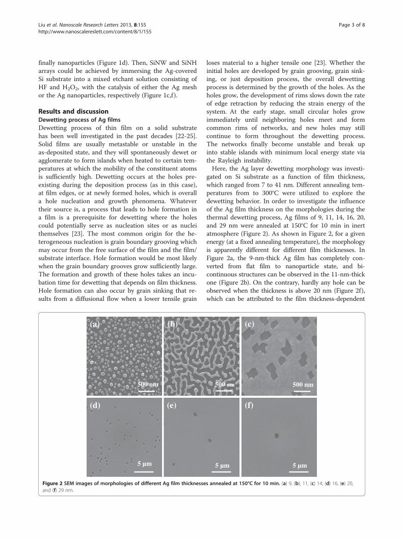
Results and discussionDewetting process of Ag filmsDewetting process of thin film on a solid substratehas been well investigated in the past decades [22-25].Solid films are usually metastable or unstable in theas-deposited state, and they will spontaneously dewet oragglomerate to form islands when heated to certain tem-peratures at which the mobility of the constituent atomsis sufficiently high. Dewetting occurs at the holes pre-existing during the deposition process (as in this case),at film edges, or at newly formed holes, which is overalla hole nucleation and growth phenomena. Whatevertheir source is, a process that leads to hole formation ina film is a prerequisite for dewetting where the holescould potentially serve as nucleation sites or as nucleithemselves [23]. The most common origin for the he-terogeneous nucleation is grain boundary grooving whichmay occur from the free surface of the film and the film/substrate interface. Hole formation would be most likelywhen the grain boundary grooves grow sufficiently large.The formation and growth of these holes takes an incu-bation time for dewetting that depends on film thickness.Hole formation can also occur by grain sinking that re-sults from a diffusional flow when a lower tensile grain
(a)
500 nm
5 µm
(b)
(d) (e)
Figure 2 SEM images of morphologies of different Ag film thicknesseand (f) 29 nm.
loses material to a higher tensile one [23]. Whether theinitial holes are developed by grain grooving, grain sink-ing, or just deposition process, the overall dewettingprocess is determined by the growth of the holes. As theholes grow, the development of rims slows down the rateof edge retraction by reducing the strain energy of thesystem. At the early stage, small circular holes growimmediately until neighboring holes meet and formcommon rims of networks, and new holes may stillcontinue to form throughout the dewetting process.The networks finally become unstable and break upinto stable islands with minimum local energy state viathe Rayleigh instability.Here, the Ag layer dewetting morphology was investi-
gated on Si substrate as a function of film thickness,which ranged from 7 to 41 nm. Different annealing tem-peratures from to 300°C were utilized to explore thedewetting behavior. In order to investigate the influenceof the Ag film thickness on the morphologies during thethermal dewetting process, Ag films of 9, 11, 14, 16, 20,and 29 nm were annealed at 150°C for 10 min in inertatmosphere (Figure 2). As shown in Figure 2, for a givenenergy (at a fixed annealing temperature), the morphologyis apparently different for different film thicknesses. InFigure 2a, the 9-nm-thick Ag film has completely con-verted from flat film to nanoparticle state, and bi-continuous structures can be observed in the 11-nm-thickone (Figure 2b). On the contrary, hardly any hole can beobserved when the thickness is above 20 nm (Figure 2f),which can be attributed to the film thickness-dependent
500 nm
5 µm
500 nm
5 µm
(c)
(f)
s annealed at 150°C for 10 min. (a) 9, (b), 11, (c) 14, (d) 16, (e) 20,
(a) (b)
(c) (d)
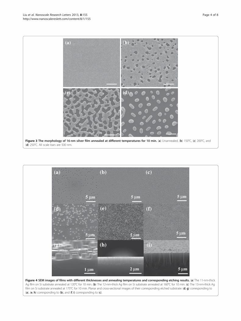
Figure 3 The morphology of 16-nm silver film annealed at different temperatures for 10 min. (a) Unannealed, (b) 150°C, (c) 200°C, and(d) 250°C. All scale bars are 500 nm.
5 µµm
5 µm
1 µm
5 µm
5 µm
2 µm
5 µm
5 µm
(a) (b) (c)
(d)
(g)
(e)
(h)
(f)
(i)
5 µm
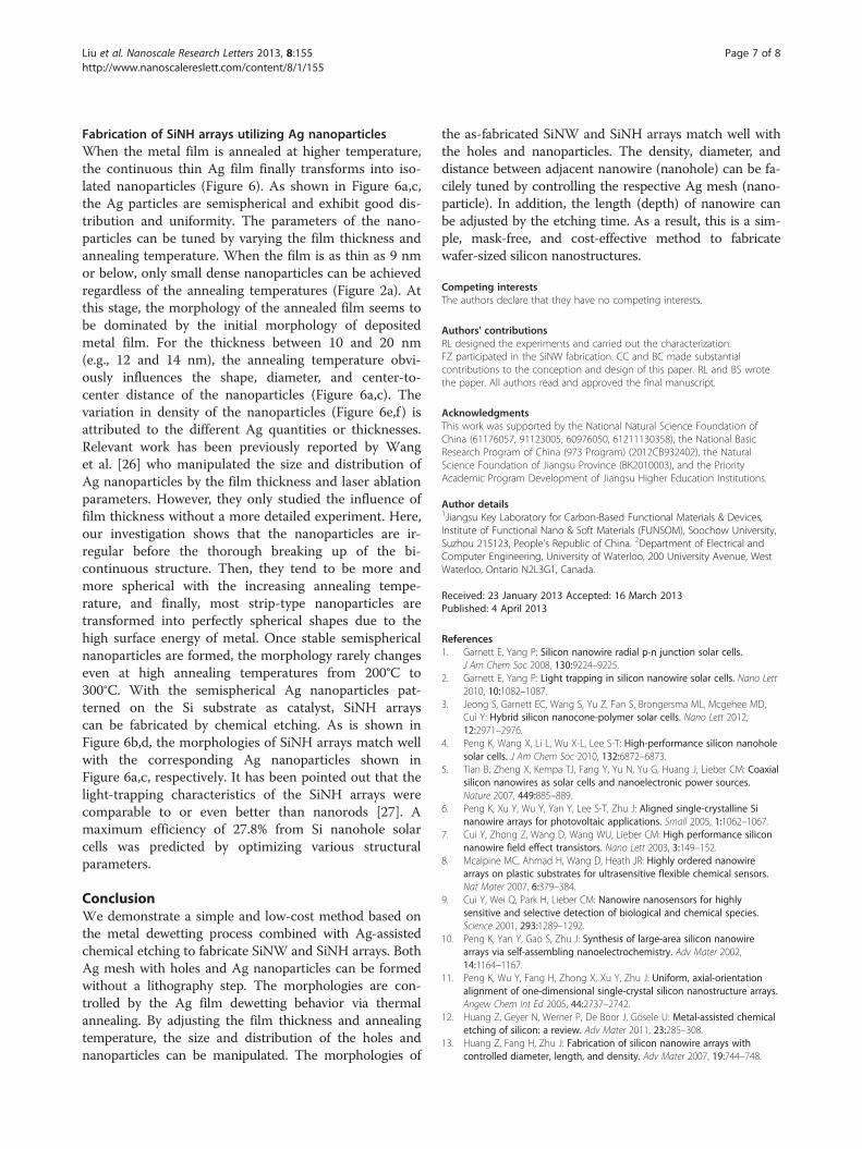
Figure 4 SEM images of films with different thicknesses and annealing temperatures and corresponding etching results. (a) The 11-nm-thickAg film on Si substrate annealed at 120°C for 10 min. (b) The 12-nm-thick Ag film on Si substrate annealed at 160°C for 10 min. (c) The 13-nm-thick Agfilm on Si substrate annealed at 175°C for 10 min. Planar and cross-sectional images of their corresponding etched substrate: (d, g) corresponding to(a), (e, h) corresponding to (b), and (f, i) corresponding to (c).
Liu et al. Nanoscale Research Letters 2013, 8:155 Page 4 of 8http://www.nanoscalereslett.com/content/8/1/155

Liu et al. Nanoscale Research Letters 2013, 8:155 Page 5 of 8http://www.nanoscalereslett.com/content/8/1/155
intermolecular forces. It was also confirmed in our experi-ment that only Ag films in the range of 10 to 20 nm couldgenerate well-distributed Ag network structure at a mod-erate temperature (approximately 150°C) [25]. Otherwise,a higher annealing temperature is indispensable to achieveAg mesh (Figure 3). It means that the temperature atwhich dewetting occurs increases with increasing metalfilm thickness. This is critical for our later step either toform SiNW arrays utilizing the Ag mesh film with holes
(a)
(c)
(e)
Figure 5 SEM images of plane-view SiNW arrays, cross-sectional SEMof plane-view SiNW arrays achieved with the catalysis of a 14-nm-thick Agthe SiNWs etched for (b) 5 min (nanowire length 0.5 μm), (c) 10 min (1 μmdistribution for the average diameters of the corresponding SiNWs.
or to form SiNH arrays utilizing Ag nanoparticles. In otherwords, the energy required to get a morphology transitionfor various film thicknesses is different, and with increas-ing thicknesses of the film, the required temperature/energy to form the metal mesh increased.Meantime, for a given film thickness (e.g., 16 nm), as the
annealing temperature increases gradually, the morpholo-gies of the film transfer from compact film to mesh onewith circular or quadrate holes (Figure 3b) and finally to
(b)
(d)
images of the SiNWs, and statistical distribution. (a) SEM imagesfilm annealed at 150°C for 10 min and cross-sectional SEM images of), and (d) 20 min (2 μm). All scale bars are 500 nm. (e) The statistical

Liu et al. Nanoscale Research Letters 2013, 8:155 Page 6 of 8http://www.nanoscalereslett.com/content/8/1/155
isolated Ag semispherical nanoparticles (Figure 3d). If thefilm is thin enough (e.g., 5 nm), only isolated island canbe achieved even at a very low annealing temperature,which may originate from the initial uncontinuousfeature during the deposition process. If the film is too thick(e.g., 41 nm), no obvious hole can be observed even forannealing temperature as high as 300°C. The dependenceof morphologies on the film thickness displays a similarbehavior. To a certain degree, the same morphology canbe achieved with different combinations of film thicknessand annealing temperature.
Fabrication of SiNW arrays utilizing Ag meshesFigure 4a,b,c shows the morphologies of dewetting Agfilms with different hole sizes. By tuning the film thick-ness and annealing temperature, the density and the di-ameters of the holes can be readily controlled. With Agmesh patterned as catalyst on silicon substrate, fabri-cation of vertical (100) SiNW arrays with controlledmorphologies were achieved, as shown in Figure 4. It isevident that the morphology of SiNWs matches well
5 µm
5 µm
(a)
(c)
(e)
Figure 6 SEM images of Ag film. (a) A 12-nm Ag film annealed at 200°C14-nm-thick Ag film annealed at 250°C for 10 min, and (d) planar view of c500 nm. (e, f) The statistical distribution for the average hole diameters for
with the shape of the corresponding holes on the Agfilms. It is interesting that not only circular (Figure 4b,c)but also quadrate (Figure 4a) cross-sectional SiNWs canbe formed using this method. The slight mismatch be-tween the Ag films and the corresponding SiNWs canbe attributed to the gradual erosion of the ultrathin Agfilm during the etching [18].Another important parameter of the SiNW arrays is
the length, which can be controlled by varying the etch-ing time. Figure 5b,c,d shows the cross-sectional scan-ning electron microscope (SEM) images of SiNW arraysfabricated with etching times of 5, 10, and 20 min, re-spectively. The Ag film is 14 nm and annealed at 150°Cfor 10 min. As a result, nanowires with lengths of about0.5 μm, about 1 μm, and about 2 μm are achieved, re-spectively. The length of the nanowires shows good li-near relationship with the duration of the etching time.The statistical analysis (Figure 5e) shows the good dia-meter distribution of the as-fabricated SiNWs. Here, thetapered morphology of the nanowires resulted from thegradual Ag dissolution-induced hole size increase.
5 µm
5 µm
(b)
(d)
(f)
for 10 min, (b) planar view of corresponding etching results to (a), (c)orresponding etching results to (c). All the scale bars of the insets are(b) and (d), respectively.
Liu et al. Nanoscale Research Letters 2013, 8:155 Page 7 of 8http://www.nanoscalereslett.com/content/8/1/155
Fabrication of SiNH arrays utilizing Ag nanoparticlesWhen the metal film is annealed at higher temperature,the continuous thin Ag film finally transforms into iso-lated nanoparticles (Figure 6). As shown in Figure 6a,c,the Ag particles are semispherical and exhibit good dis-tribution and uniformity. The parameters of the nano-particles can be tuned by varying the film thickness andannealing temperature. When the film is as thin as 9 nmor below, only small dense nanoparticles can be achievedregardless of the annealing temperatures (Figure 2a). Atthis stage, the morphology of the annealed film seems tobe dominated by the initial morphology of depositedmetal film. For the thickness between 10 and 20 nm(e.g., 12 and 14 nm), the annealing temperature obvi-ously influences the shape, diameter, and center-to-center distance of the nanoparticles (Figure 6a,c). Thevariation in density of the nanoparticles (Figure 6e,f ) isattributed to the different Ag quantities or thicknesses.Relevant work has been previously reported by Wanget al. [26] who manipulated the size and distribution ofAg nanoparticles by the film thickness and laser ablationparameters. However, they only studied the influence offilm thickness without a more detailed experiment. Here,our investigation shows that the nanoparticles are ir-regular before the thorough breaking up of the bi-continuous structure. Then, they tend to be more andmore spherical with the increasing annealing tempe-rature, and finally, most strip-type nanoparticles aretransformed into perfectly spherical shapes due to thehigh surface energy of metal. Once stable semisphericalnanoparticles are formed, the morphology rarely changeseven at high annealing temperatures from 200°C to300°C. With the semispherical Ag nanoparticles pat-terned on the Si substrate as catalyst, SiNH arrayscan be fabricated by chemical etching. As is shown inFigure 6b,d, the morphologies of SiNH arrays match wellwith the corresponding Ag nanoparticles shown inFigure 6a,c, respectively. It has been pointed out that thelight-trapping characteristics of the SiNH arrays werecomparable to or even better than nanorods [27]. Amaximum efficiency of 27.8% from Si nanohole solarcells was predicted by optimizing various structuralparameters.
ConclusionWe demonstrate a simple and low-cost method based onthe metal dewetting process combined with Ag-assistedchemical etching to fabricate SiNW and SiNH arrays. BothAg mesh with holes and Ag nanoparticles can be formedwithout a lithography step. The morphologies are con-trolled by the Ag film dewetting behavior via thermalannealing. By adjusting the film thickness and annealingtemperature, the size and distribution of the holes andnanoparticles can be manipulated. The morphologies of
the as-fabricated SiNW and SiNH arrays match well withthe holes and nanoparticles. The density, diameter, anddistance between adjacent nanowire (nanohole) can be fa-cilely tuned by controlling the respective Ag mesh (nano-particle). In addition, the length (depth) of nanowire canbe adjusted by the etching time. As a result, this is a sim-ple, mask-free, and cost-effective method to fabricatewafer-sized silicon nanostructures.
Competing interestsThe authors declare that they have no competing interests.
Authors' contributionsRL designed the experiments and carried out the characterization.FZ participated in the SiNW fabrication. CC and BC made substantialcontributions to the conception and design of this paper. RL and BS wrotethe paper. All authors read and approved the final manuscript.
AcknowledgmentsThis work was supported by the National Natural Science Foundation ofChina (61176057, 91123005, 60976050, 61211130358), the National BasicResearch Program of China (973 Program) (2012CB932402), the NaturalScience Foundation of Jiangsu Province (BK2010003), and the PriorityAcademic Program Development of Jiangsu Higher Education Institutions.
Author details1Jiangsu Key Laboratory for Carbon-Based Functional Materials & Devices,Institute of Functional Nano & Soft Materials (FUNSOM), Soochow University,Suzhou 215123, People's Republic of China. 2Department of Electrical andComputer Engineering, University of Waterloo, 200 University Avenue, WestWaterloo, Ontario N2L3G1, Canada.
Received: 23 January 2013 Accepted: 16 March 2013Published: 4 April 2013
References1. Garnett E, Yang P: Silicon nanowire radial p-n junction solar cells.
J Am Chem Soc 2008, 130:9224–9225.2. Garnett E, Yang P: Light trapping in silicon nanowire solar cells. Nano Lett
2010, 10:1082–1087.3. Jeong S, Garnett EC, Wang S, Yu Z, Fan S, Brongersma ML, Mcgehee MD,
Cui Y: Hybrid silicon nanocone-polymer solar cells. Nano Lett 2012,12:2971–2976.
4. Peng K, Wang X, Li L, Wu X-L, Lee S-T: High-performance silicon nanoholesolar cells. J Am Chem Soc 2010, 132:6872–6873.
5. Tian B, Zheng X, Kempa TJ, Fang Y, Yu N, Yu G, Huang J, Lieber CM: Coaxialsilicon nanowires as solar cells and nanoelectronic power sources.Nature 2007, 449:885–889.
6. Peng K, Xu Y, Wu Y, Yan Y, Lee S-T, Zhu J: Aligned single-crystalline Sinanowire arrays for photovoltaic applications. Small 2005, 1:1062–1067.
7. Cui Y, Zhong Z, Wang D, Wang WU, Lieber CM: High performance siliconnanowire field effect transistors. Nano Lett 2003, 3:149–152.
8. Mcalpine MC, Ahmad H, Wang D, Heath JR: Highly ordered nanowirearrays on plastic substrates for ultrasensitive flexible chemical sensors.Nat Mater 2007, 6:379–384.
9. Cui Y, Wei Q, Park H, Lieber CM: Nanowire nanosensors for highlysensitive and selective detection of biological and chemical species.Science 2001, 293:1289–1292.
10. Peng K, Yan Y, Gao S, Zhu J: Synthesis of large-area silicon nanowirearrays via self-assembling nanoelectrochemistry. Adv Mater 2002,14:1164–1167.
11. Peng K, Wu Y, Fang H, Zhong X, Xu Y, Zhu J: Uniform, axial-orientationalignment of one-dimensional single-crystal silicon nanostructure arrays.Angew Chem Int Ed 2005, 44:2737–2742.
12. Huang Z, Geyer N, Werner P, De Boor J, Gösele U: Metal-assisted chemicaletching of silicon: a review. Adv Mater 2011, 23:285–308.
13. Huang Z, Fang H, Zhu J: Fabrication of silicon nanowire arrays withcontrolled diameter, length, and density. Adv Mater 2007, 19:744–748.

Liu et al. Nanoscale Research Letters 2013, 8:155 Page 8 of 8http://www.nanoscalereslett.com/content/8/1/155
14. Peng K, Zhang M, Lu A, Wong N-B, Zhang R, Lee S-T: Ordered siliconnanowire arrays via nanosphere lithography and metal-induced etching.Appl Phys Lett 2007, 90:163123–3.
15. Choi WK, Liew TH, Dawood MK, Smith HI, Thompson CV, Hong MH:Synthesis of silicon nanowires and nanofin arrays using interferencelithography and catalytic etching. Nano Lett 2008, 8:3799–3802.
16. Boor J, Geyer N, Wittemann JV, Gosele U, Schmidt V: Sub-100 nm siliconnanowires by laser interference lithography and metal-assisted etching.Nanotechnology 2010, 21:095302.
17. Chang S-W, Chuang VP, Boles ST, Ross CA, Thompson CV: Densely packedarrays of ultra-high-aspect-ratio silicon nanowires fabricated using block-copolymer lithography and metal-assisted etching. Adv Funct Mater 2009,19:2495–2500.
18. Huang Z, Zhang X, Reiche M, Liu L, Lee W, Shimizu T, Senz S, Gö Sele U:Extended arrays of vertically aligned sub-10 nm diameter [100] Sinanowires by metal-assisted chemical etching. Nano Lett 2008,8:3046–3051.
19. Huang Z, Tomohiro S, Senz S, Zhang Z, Xuanxiong Z, Lee W, Nadinr G, GöSele U: Ordered arrays of vertically aligned [110] silicon nanowires bysupressing the crystallographilly preferred <100> etching directions.Nano Lett 2009, 9:2519–2525.
20. Kim J, Han H, Kim YH, Choi S-H, Kim J-C, Lee W: Au/Ag bilayered metalmesh as a Si etching catalyst for controlled fabrication of Si nanowires.ACS Nano 2011, 5:3222–3229.
21. Peng K-Q, Wang X, Wu X, Lee S-T: Fabrication and photovoltaic propertyof ordered macroporous silicon. Appl Phys Lett 2009, 95:143119.
22. Bischof J, Scherer D, Herminghaus S, Leiderer P: Dewetting modes of thinmetallic films: nucleation of holes and spinodal dewetting. Phys Rev Lett1996, 77:1536–1539.
23. Srolovitz D, Goldiner M: The thermodynamics and kinetics of filmagglomeration. JOM 1995, 47:31–36.
24. Thompson CV: Solid-state dewetting of thin films. Ann Rev Mater Res 2012,42:399–434.
25. Krishna H, Sachan R, Strader J, Favazza C, Khenner M, Kalyanaraman R:Thickness-dependent spontaneous dewetting morphology of ultrathinAg films. Nanotechnology 2010, 21:155601.
26. Wang F, Yu HY, Wang X, Li J, Sun X, Yang M, Wong SM, Zheng H: Masklessfabrication of large scale Si nanohole array via laser annealed metalnanoparticles catalytic etching for photovoltaic application.J Appl Phys 2010, 108:024301.
27. Han SE, Chen G: Optical absorption enhancement in silicon nanoholearrays for solar photovoltaics. Nano Lett 2010, 10:1012–1015.
doi:10.1186/1556-276X-8-155Cite this article as: Liu et al.: Lithography-free fabrication of siliconnanowire and nanohole arrays by metal-assisted chemical etching.Nanoscale Research Letters 2013 8:155.
Submit your manuscript to a journal and benefi t from:
7 Convenient online submission
7 Rigorous peer review
7 Immediate publication on acceptance
7 Open access: articles freely available online
7 High visibility within the fi eld
7 Retaining the copyright to your article
Submit your next manuscript at 7 springeropen.com