mumps design handbook - university of california,...
TRANSCRIPT
MUMPs™
Design Handbook
Revision 4.0
David A. KoesterRamaswamy Mahadevan
Alex Shishkoffand
Karen W. Markus
Cronos Integrated Microsystems3021 Cornwallis Road
Research Triangle Park, NC 27709May 1999

Copyright © 1999 by Cronos Integrated Microsystems. All rights reserved.
Permission to use, copy, and modify for internal, noncommercial purposesis hereby granted. Any distribution of this manual or associated layouts orany part thereof is strictly prohibited without prior written consent ofMCNC.
GDSII is a trademark of Calma, Valid, Cadence.
L-Edit and Tanner Database are trademarks of Tanner Research Inc.
Chapter 1 Three Layer Polysilicon Surface MicromachiningProcess.................................................................................. 1
1.1 Introduction ..................................................................................................... 1
1.2 Process Overview............................................................................................ 2
Chapter 2 MUMPs™ Design Guidelines and Rules .......................... 92.1 Design Rules and Considerations.................................................................... 9
2.2 Design Rules.................................................................................................. 10
2.3 Process and Design Issues (or Hints and Pitfalls) ......................................... 29
2.4 Film Parameters............................................................................................. 33
2.5 EZ-MUMPs™ Design Rules.......................................................................... 35
2.6 Layout Submission ........................................................................................ 36
2.7 Custom Dicing, Releasing, and Critical Point Drying .................................. 37
MUMPs™ Design Handbook – 5/26/99 1
Chapter 1 Three-Layer PolysiliconSurface MicromachiningProcess
1.1 Introduction
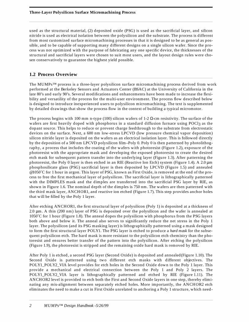
The Multi-User MEMS Processes or MUMPs™ is a commercial program that provides the internationalindustrial, governmental and academic communities with cost-effective, proof-of-concept surfacemicromachining fabrication. MUMPs™ is designed for general purpose micromachining by outsideusers who would like to fabricate MEMS devices. The following is a general description of theMUMPs™ process geared toward users of the MUMPs™ service who may not have a strong backgroundin microfabrication, but it contains information that is useful to all MUMPs™ users.
Figure 1.1. Cross sectional view showing all 7 layers of the MUMPs™ process (not to scale).
Figure 1.1 is a cross section of the three-layer polysilicon surface micromachining MUMPs™ process.This process has the general features of a standard surface micromachining process: (1) polysilicon is
Three-Layer Polysilicon Surface Micromachining Process
2 MUMPs™ Design Handbook -5/26/99
used as the structural material, (2) deposited oxide (PSG) is used as the sacrificial layer, and siliconnitride is used as electrical isolation between the polysilicon and the substrate. The process is differentfrom most customized surface micromachining processes in that it is designed to be as general as pos-sible, and to be capable of supporting many different designs on a single silicon wafer. Since the pro-cess was not optimized with the purpose of fabricating any one specific device, the thicknesses of thestructural and sacrificial layers were chosen to suit most users, and the layout design rules were cho-sen conservatively to guarantee the highest yield possible.
1.2 Process Overview
The MUMPs™ process is a three-layer polysilicon surface micromachining process derived from workperformed at the Berkeley Sensors and Actuators Center (BSAC) at the University of California in thelate 80’s and early 90’s. Several modifications and enhancements have been made to increase the flexi-bility and versatility of the process for the multi-user environment. The process flow described belowis designed to introduce inexperienced users to polysilicon micromachining. The text is supplementedby detailed drawings that show the process flow in the context of building a typical micromotor.
The process begins with 100 mm n-type (100) silicon wafers of 1-2 Ω-cm resistivity. The surface of thewafers are first heavily doped with phosphorus in a standard diffusion furnace using POCl3 as thedopant source. This helps to reduce or prevent charge feedthrough to the substrate from electrostaticdevices on the surface. Next, a 600 nm low-stress LPCVD (low pressure chemical vapor deposition)silicon nitride layer is deposited on the wafers as an electrical isolation layer. This is followed directlyby the deposition of a 500 nm LPCVD polysilicon film–Poly 0. Poly 0 is then patterned by photolithog-raphy, a process that includes the coating of the wafers with photoresist (Figure 1.2), exposure of thephotoresist with the appropriate mask and developing the exposed photoresist to create the desiredetch mask for subsequent pattern transfer into the underlying layer (Figure 1.3). After patterning thephotoresist, the Poly 0 layer is then etched in an RIE (Reactive Ion Etch) system (Figure 1.4). A 2.0 µmphosphosilicate glass (PSG) sacrificial layer is then deposited by LPCVD (Figure 1.5) and annealed@1050˚C for 1 hour in argon. This layer of PSG, known as First Oxide, is removed at the end of the pro-cess to free the first mechanical layer of polysilicon. The sacrificial layer is lithographically patternedwith the DIMPLES mask and the dimples are transferred into the sacrificial PSG layer by RIE, asshown in Figure 1.6. The nominal depth of the dimples is 750 nm. The wafers are then patterned withthe third mask layer, ANCHOR1, and reactive ion etched (Figure 1.7). This step provides anchor holesthat will be filled by the Poly 1 layer.
After etching ANCHOR1, the first structural layer of polysilicon (Poly 1) is deposited at a thickness of2.0 µm. A thin (200 nm) layer of PSG is deposited over the polysilicon and the wafer is annealed at1050˚C for 1 hour (Figure 1.8). The anneal dopes the polysilicon with phosphorus from the PSG layersboth above and below it. The anneal also serves to significantly reduce the net stress in the Poly 1layer. The polysilicon (and its PSG masking layer) is lithographically patterned using a mask designedto form the first structural layer POLY1. The PSG layer is etched to produce a hard mask for the subse-quent polysilicon etch. The hard mask is more resistant to the polysilicon etch chemistry than the pho-toresist and ensures better transfer of the pattern into the polysilicon. After etching the polysilicon(Figure 1.9), the photoresist is stripped and the remaining oxide hard mask is removed by RIE.
After Poly 1 is etched, a second PSG layer (Second Oxide) is deposited and annealed(Figure 1.10). TheSecond Oxide is patterned using two different etch masks with different objectives. ThePOLY1_POLY2_VIA level provides for etch holes in the Second Oxide down to the Poly 1 layer. Thisprovide a mechanical and electrical connection between the Poly 1 and Poly 2 layers. ThePOLY1_POLY2_VIA layer is lithographically patterned and etched by RIE (Figure 1.11). TheANCHOR2 level is provided to etch both the First and Second Oxide layers in one step, thereby elimi-nating any mis-alignment between separately etched holes. More importantly, the ANCHOR2 etcheliminates the need to make a cut in First Oxide unrelated to anchoring a Poly 1 structure, which need-
Process Overview
MUMPs™ Design Handbook – 5/26/99 3
lessly exposes the substrate to subsequent processing that can damage either Poly 0 or Nitride (seeSection 2.3.3). The ANCHOR2 layer is lithographically patterned and etched by RIE in the same wayas POLY1_POLY2_VIA.
Figure 1.12 shows the wafer cross section after both POLY1_POLY2_VIA and ANCHOR2 levelshave been completed. The second structural layer, Poly 2, is then deposited (1.5 µm thick) followedby the deposition of 200 nm PSG. As with Poly 1, the thin PSG layer acts as both an etch mask anddopant source for Poly 2 (Figure 1.13). The wafer is annealed for one hour at 1050 C to dope thepolysilicon and reduce the residual film stress. The Poly 2 layer is lithographically patterned with theseventh mask (POLY2) and the PSG and polysilicon layers are etched by RIE using the sameprocessing conditions as for Poly 1. The photoresist then is stripped and the masking oxide isremoved (Figure 1.14).
The final deposited layer in the MUMPs™ process is a 0.5 µm metal layer that provides for probing,bonding, electrical routing and highly reflective mirror surfaces. The wafer is patterned lithographi-cally with the eighth mask (METAL) and the metal is deposited and patterned using lift-off. Thefinal, unreleased structure is shown in Figure 1.15. The wafers are diced, sorted and shipped to theMUMPs™ user for sacrificial release and test. Figure 1.16 shows the device after sacrificial oxiderelease. The release is performed by immersing the chip in a bath of 49% HF (room temperature) for1.5-2 minutes. This is followed by several minutes in DI water and then alcohol to reduce stictionfollowed by at least 10 minutes in an oven at 1100 C.
Generally the participants receive their dice and perform the sacrificial oxide release in their ownfacility. For those participants who request it, release of their dice at Cronos’ facility can be arrangedfor an additional fee.
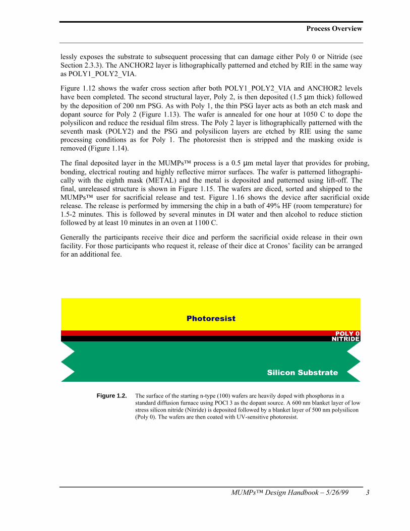
Figure 1.2. The surface of the starting n-type (100) wafers are heavily doped with phosphorus in astandard diffusion furnace using POCl 3 as the dopant source. A 600 nm blanket layer of lowstress silicon nitride (Nitride) is deposited followed by a blanket layer of 500 nm polysilicon(Poly 0). The wafers are then coated with UV-sensitive photoresist.
Three-Layer Polysilicon Surface Micromachining Process
4 MUMPs™ Design Handbook – 5/26/99
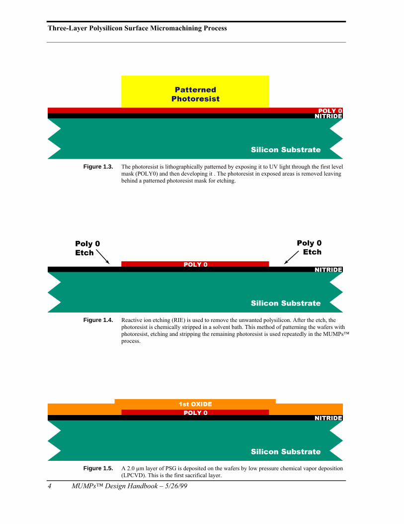
Figure 1.3. The photoresist is lithographically patterned by exposing it to UV light through the first levelmask (POLY0) and then developing it . The photoresist in exposed areas is removed leavingbehind a patterned photoresist mask for etching.
Figure 1.4. Reactive ion etching (RIE) is used to remove the unwanted polysilicon. After the etch, thephotoresist is chemically stripped in a solvent bath. This method of patterning the wafers withphotoresist, etching and stripping the remaining photoresist is used repeatedly in the MUMPs™process.
Figure 1.5. A 2.0 µm layer of PSG is deposited on the wafers by low pressure chemical vapor deposition(LPCVD). This is the first sacrifical layer.
Process Overview
MUMPs™ Design Handbook – 5/26/99 5
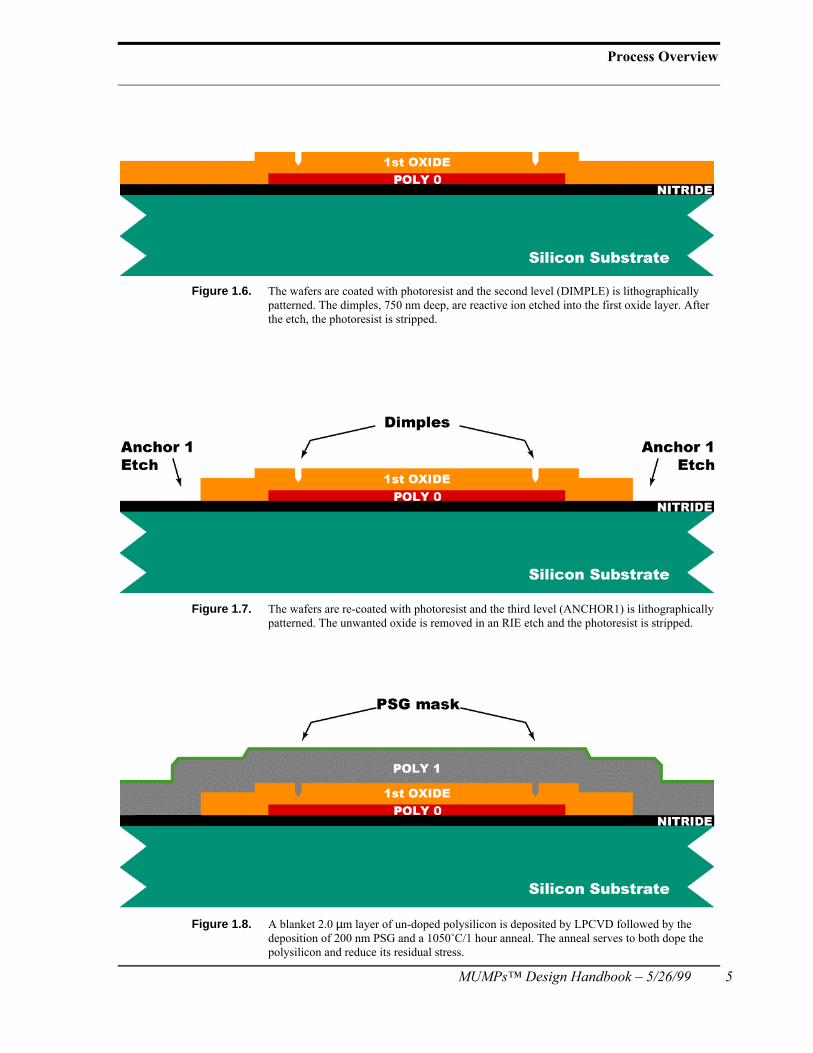
Figure 1.6. The wafers are coated with photoresist and the second level (DIMPLE) is lithographicallypatterned. The dimples, 750 nm deep, are reactive ion etched into the first oxide layer. Afterthe etch, the photoresist is stripped.
Figure 1.7. The wafers are re-coated with photoresist and the third level (ANCHOR1) is lithographicallypatterned. The unwanted oxide is removed in an RIE etch and the photoresist is stripped.
Figure 1.8. A blanket 2.0 µm layer of un-doped polysilicon is deposited by LPCVD followed by thedeposition of 200 nm PSG and a 1050˚C/1 hour anneal. The anneal serves to both dope thepolysilicon and reduce its residual stress.

Three-Layer Polysilicon Surface Micromachining Process
6 MUMPs™ Design Handbook – 5/26/99
Figure 1.9. The wafer is coated with photoresist and the fourth level (POLY1) is lithographicallypatterned. The PSG is first etched to create a hard mask and then Poly 1 is etched by RIE.After the etch is completed, the photoresist and PSG hard mask are removed.
Figure 1.10. The Second Oxide layer, 0.75 µm of PSG, is deposited on the wafer. This layer is patternedtwice to allow contact to both Poly 1 and substrate layers.
Figure 1.11. The wafer is coated with photoresist and the fifth level (POLY1_POLY2_VIA) islithographically patterned. The unwanted Second Oxide is RIE etched, stopping on Poly 1,and the photoresist is stripped.

Process Overview
MUMPs™ Design Handbook – 5/26/99 7
Figure 1.12. The wafer is re-coated with photoresist and the sixth level (ANCHOR2) is lithographically patterned.The Second and First Oxides are RIE etched, stopping on either Nitride or Poly 0, and the photoresistis stripped. The ANCHOR2 level provides openings for Poly 2 to contact with Nitride or Poly 0.
Figure 1.13. A 1.5 µm un-doped polysilicon layer is deposited follwed by a 200 nm PSG hardmask layer. Thewafers are annealed at 1050˚C for one hour to dope the polysilicon and reduce residual stress.
Figure 1.14. The wafer is coated with photoresist and the seventh level (POLY2) is lithographically patterned. ThePSG hard mask and Poly 2 layers are RIE etched and the photoresist and hard mask are removed. Allmechanical structures have now been fabricated. The remaining steps are to deposit the metal layer andremove the sacrificial oxides
Three-Layer Polysilicon Surface Micromachining Process
8 MUMPs™ Design Handbook – 5/26/99
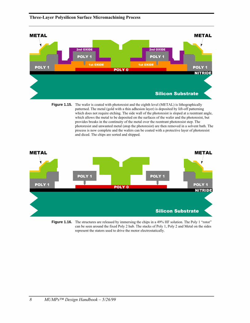
Figure 1.15. The wafer is coated with photoresist and the eighth level (METAL) is lithographicallypatterned. The metal (gold with a thin adhesion layer) is deposited by lift-off patterningwhich does not require etching. The side wall of the photoresist is sloped at a reentrant angle,which allows the metal to be deposited on the surfaces of the wafer and the photoresist, butprovides breaks in the continuity of the metal over the reentrant photoresist step. Thephotoresist and unwanted metal (atop the photoresist) are then removed in a solvent bath. Theprocess is now complete and the wafers can be coated with a protective layer of photoresistand diced. The chips are sorted and shipped.
Figure 1.16. The structures are released by immersing the chips in a 49% HF solution. The Poly 1 “rotor”can be seen around the fixed Poly 2 hub. The stacks of Poly 1, Poly 2 and Metal on the sidesrepresent the stators used to drive the motor electrostatically.
MUMPs™ Design Handbook - 5/21/99 9
Chapter 2 MUMPs™ Design Guidelines and Rules
2.1 Design Rules and Considerations
2.1.1 Introduction
The purpose of the design rules is to ensure the greatest possibility of successful fabrication. The ruleshave evolved through process development, the experience of the Cronos staff, and most importantly,experience from previous MUMPs™ runs. The design rules are a set of requirements and advisementsthat are defined by the limits of the process (i.e. the stable process window) which in turn is defined bythe capabilities of the individual process steps. In general, minimum design rules are defined by theresolution and alignment capabilities of the lithography system. This section of the documentdescribes the design rules, both mandatory and advisory, that exist for the MUMPs™ three-layer polysil-icon micromachining process.
Design rules in the document define the minimum feature sizes and spaces for all levels and minimumoverlap and spacing between relevant levels. The minimum line widths and spaces are mandatoryrules . Mandatory rules are given to ensure that all layouts will remain compatible with Cronos’s litho-graphic process tolerances. Violation of minimum line/space rules will result in missing, undersized,oversized or fused features. Minimum overlap (enclosure, cut-in and cutout rules) requirementsreduce the effect of large topographies and prevent unnecessary etching of underlying layers. Mini-mum spacing between levels guarantees that features of two different levels can be delineated by pho-tolithography and etch. Please note: The minimum geometry allowed should not be confused withthe nominal geometry a designer uses. Minimum geometries should only be used where absolutelynecessary. When size is not an issue, the feature should be designed larger than the minimum allowedvalue.
In general, the enclosure and interlevel spacing rules are advisory rules. Cronos recognizes that theremay be valid reasons requiring that an enclosure or interlevel spacing rule be violated. We also recog-nize the limitations of our process and equipment. As such, we try to explain why an advisory ruleexists and the possible or probable consequence of violating it. We allow users to ignore the advisory rules,
MUMPs™ Design Guidelines and Rules
10 MUMPs™ Design Handbook - 5/21/99
but at their own risk. Cronos is not responsible for the possible processing consequence of violating anadvisory rule.
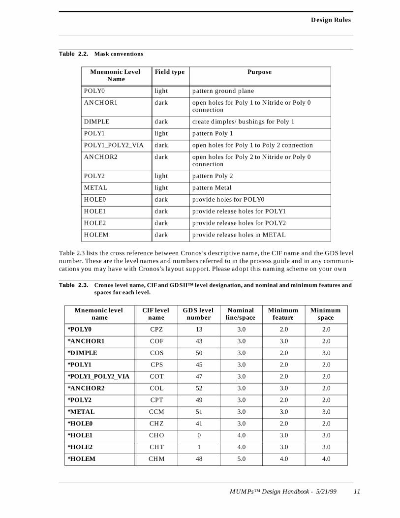
A word on the conventions followed in this document. Lithography levels (i.e. names for each mask-ing level) will be written in upper case. When referring to a specific layer of material, be it oxide orpolysilicon, the material will be typed in lower case with the first letter capitalized. For examplePOLY1 refers to the masking level for patterning the first polysilicon layer. Table 2.1 outlines the mate-rial layer names, thicknesses and the lithography levels associated with those layers.
Table 2.1. Layer names, thicknesses and lithography levels. Hole levels are printed on the same line as their corresponding polysilicon or metal levels.
2.2 Design Rules
The design rules for the MUMPs™ process are described both in tabular form and in schematic draw-ings. The tables list the rules and give references to the specific figure in which the rule is described.There are 14 mandatory rules. These are highlighted with an asterisk (*) in the tables and printed inbold text to help distinguish them. All other rules are cautionary guidelines (advisory rules) whichshould only be violated for specific desired applications1.
Table 2.2 lists the field convention used in the Cronos process and a brief description of the purpose ofeach level. All polysilicon levels are light field and all oxide levels are dark field. [Please note that thedata should always be drawn (digitized) as described in the rules and not based upon your historicalunderstanding of the light and dark field conventions. Too often the terms light field and dark fieldmean different things in different facilities. The convention used here is that accepted by the commer-cial mask maker used by Cronos.] In light field levels, draw the feature–the object you want leftbehind after the etch. In dark field levels, draw the holes–the areas you want to etch away. For exam-ple, POLY0 is a light field level. When drawing POLY0, you will draw (digitize) the poly structures.When drawing ANCHOR1, a dark field level, you will draw the holes that will later serve as Poly 1anchor holes. Please pay special attention to this concept. Failure to comply with this convention willresult in layer polarity reversals.
1. Cronos is not responsible for process consequences that might result from violating either mandatory or advi-sory rules.
Material Layer Thickness ( µm) Lithography Level Name
Nitride 0.6 --
Poly 0 0.5 POLY0 (HOLE0)
First Oxide 2.0DIMPLE
ANCHOR1
Poly 1 2.0 POLY1 (HOLE1)
Second Oxide 0.75POLY1_POLY2_VIA
ANCHOR2
Poly 2 1.5 POLY2 (HOLE2)
Metal 0.5 METAL (HOLEM)
Design Rules
MUMPs™ Design Handbook - 5/21/99 11
Table 2.2. Mask conventions
Table 2.3 lists the cross reference between Cronos’s descriptive name, the CIF name and the GDS levelnumber. These are the level names and numbers referred to in the process guide and in any communi-cations you may have with Cronos’s layout support. Please adopt this naming scheme on your own
Table 2.3. Cronos level name, CIF and GDSII™ level designation, and nominal and minimum features and spaces for each level.
Mnemonic Level Name
Field type Purpose
POLY0 light pattern ground plane
ANCHOR1 dark open holes for Poly 1 to Nitride or Poly 0 connection
DIMPLE dark create dimples/bushings for Poly 1
POLY1 light pattern Poly 1
POLY1_POLY2_VIA dark open holes for Poly 1 to Poly 2 connection
ANCHOR2 dark open holes for Poly 2 to Nitride or Poly 0 connection
POLY2 light pattern Poly 2
METAL light pattern Metal
HOLE0 dark provide holes for POLY0
HOLE1 dark provide release holes for POLY1
HOLE2 dark provide release holes for POLY2
HOLEM dark provide release holes in METAL
Mnemonic levelname
CIF levelname
GDS level number
Nominal line/space
Minimum feature
Minimum space
*POLY0 CPZ 13 3.0 2.0 2.0
*ANCHOR1 COF 43 3.0 3.0 2.0
*DIMPLE COS 50 3.0 2.0 3.0
*POLY1 CPS 45 3.0 2.0 2.0
*POLY1_POLY2_VIA COT 47 3.0 2.0 2.0
*ANCHOR2 COL 52 3.0 3.0 2.0
*POLY2 CPT 49 3.0 2.0 2.0
*METAL CCM 51 3.0 3.0 3.0
*HOLE0 CHZ 41 3.0 2.0 2.0
*HOLE1 CHO 0 4.0 3.0 3.0
*HOLE2 CHT 1 4.0 3.0 3.0
*HOLEM CHM 48 5.0 4.0 4.0
MUMPs™ Design Guidelines and Rules
12 MUMPs™ Design Handbook - 5/21/99
layout system to minimize confusion when you transfer your data file to Cronos for fabrication. Thetable also lists the nominal feature/space and the minimum feature and space allowable for that level.These minimum features and spacings are mandatory rules.
The hole layers (HOLE0, HOLE1, HOLE2 and HOLEM) for POLY0, POLY1, POLY2 and METAL,respectively, are shown as separate levels in order to make layout of POLY0, POLY1, POLY2 andMETAL easier. The principal purpose of these holes (except for HOLE0) is to provide shorter releaseetch paths under large polysilicon features. The secondary purpose is to provide a simple way to“extract” holes from a light field level. The drawing of holes in a large digitized (drawn) level can bedifficult, or even impossible with some layout systems. Cronos has chosen to define unique levels fordrawing holes to simplify this process. You need only draw the physical polysilicon or metal structurewithout the holes, then draw (digitize) the desired etch hole on the corresponding HOLE level andCronos will superimpose the two levels. Table 2.1 and Table 2.2 indicate the proper correspondencebetween layers. Since hole levels are actually part of their corresponding light field levels (e.g. HOLE0is part of POLY0), all holes are subject to the same dimension and alignment rules as the correspond-ing level. Do not use the hole layers to defi ne geometries other than etch holes!
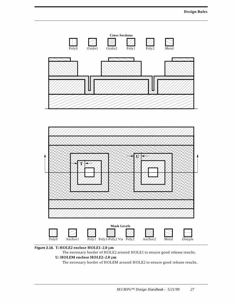
One important note about etch holes. In cases where you are stacking layers (e.g. Metal on Poly 2), theetch holes must be aligned. In addition, for best results, the holes of the upper layer should enclose theholes of the lower layer by 2.0 µm (see rules T and U).
It should be noted that the photo masking process used by Cronos is capable of rendering arcs andnon-rectangular polygons. You are welcome and encouraged to include non-Manhattan geometries aspart of your submission. Keep in mind, however, that the masks are printed with a 0.25 µm spot sizeand all features are limited by this registration. To minimize vertex snapping errors in the fracturing ofthe data, please use a 0.25 micron grid in layout and avoid rotating cells. Please refer to Section 2.6 onpage 35 for other layout guidelines.
The level to level design rules are listed in three tables: Table 2.4 lists the design rules pertaining to thePOLY0, Table 2.5 lists the rules pertaining to POLY1 and DIMPLES and Table 2.6 lists the rules forPOLY2. The rules are given in each line of the table along with a figure number and a rule letter. Fig-ures 2.5 through 2.16 are cross sections and plan views of the rules. The 21 rule letters point out whichdimensions on the plan view pertain to the specific rule, and the corresponding verbal explanation ofthat rule. Please note that the drawings show how the films relate to each other up to that point of pro-cessing. For clarity, the drawings do not necessarily represent true or completed structures. Also ofimportance, the plan views show the drawn (digitized) layout and cross sections show the resultingstructures . This should help you better visualize the rules in layout form. The fill patterns for the planand cross section views are slightly different since, in the case of dark field levels, the drawn feature inplan view is actually a hole, i.e. the absence of material. On most figures, the fill patterns are shown onthe same page.
2.2.1 Rule Nomenclature
This document uses nomenclature that may not be familiar to some users. The nomenclature is basedon Boolean operators that are used in the design rule checker. There are four basic operators used todescribe the rules: enclose, spacing, cut-inside and cut-outside. The following diagrams explain thenomenclature and describe the operators and rule.
Design Rules
MUMPs™ Design Handbook – 5/26/99 13
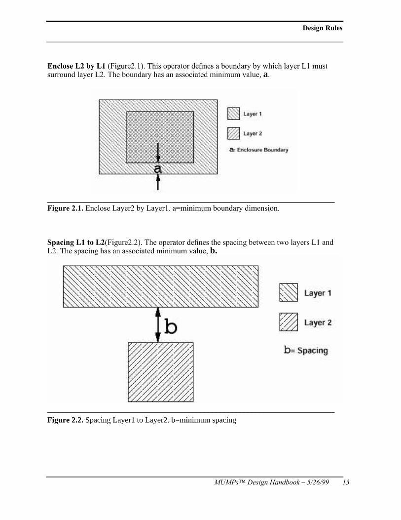
Enclose L2 by L1 (Figure2.1). This operator defines a boundary by which layer L1 mustsurround layer L2. The boundary has an associated minimum value, a.
_________________________________________________________________________Figure 2.1. Enclose Layer2 by Layer1. a=minimum boundary dimension.
Spacing L1 to L2(Figure2.2). The operator defines the spacing between two layers L1 andL2. The spacing has an associated minimum value, b.
_________________________________________________________________________Figure 2.2. Spacing Layer1 to Layer2. b=minimum spacing
MUMPs™ Design Guidelines and Rules
14 MUMPs™ Design Handbook – 5/26/99
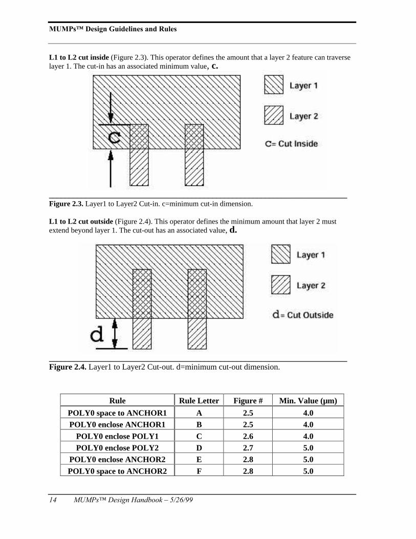
L1 to L2 cut inside (Figure 2.3). This operator defines the amount that a layer 2 feature can traverselayer 1. The cut-in has an associated minimum value, c.
_________________________________________________________________________Figure 2.3. Layer1 to Layer2 Cut-in. c=minimum cut-in dimension.
L1 to L2 cut outside (Figure 2.4). This operator defines the minimum amount that layer 2 mustextend beyond layer 1. The cut-out has an associated value, d.
_________________________________________________________________________Figure 2.4. Layer1 to Layer2 Cut-out. d=minimum cut-out dimension.
Rule Rule Letter Figure # Min. Value (µm)
POLY0 space to ANCHOR1 A 2.5 4.0POLY0 enclose ANCHOR1 B 2.5 4.0
POLY0 enclose POLY1 C 2.6 4.0POLY0 enclose POLY2 D 2.7 5.0
POLY0 enclose ANCHOR2 E 2.8 5.0POLY0 space to ANCHOR2 F 2.8 5.0
Design Rules
MUMPs™ Design Handbook - 5/21/99 15
Table 2.4 contains the rules that relate to POLY0. The Poly 0 layer is typically used as a ground plane orfor routing purposes. The use of this layer is optional, and may not be needed. Rules A and B ensureproper placement of ANCHOR1 with respect to POLY0. Rules C and D define proper enclosure ofPOLY1 and POLY2. Rules E and F ensure proper placement of ANCHOR2 with respect to POLY0.
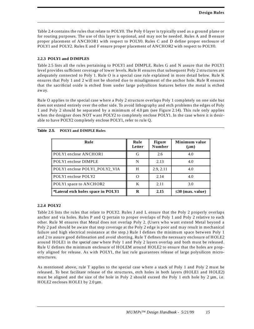
2.2.3 POLY1 and DIMPLES
Table 2.5 lists all the rules pertaining to POLY1 and DIMPLE. Rules G and N assure that the POLY1level provides sufficient coverage of lower levels. Rule H ensures that subsequent Poly 2 structures areadequately connected to Poly 1. Rule O is a special case rule explained in more detail below. Rule Kensures that Poly 1 and 2 will not be shorted due to misalignment of the anchor hole. Rule R ensuresthat the sacrificial oxide is etched from under large polysilicon features before the metal is etchedaway.
Rule O applies to the special case where a Poly 2 structure overlaps Poly 1 completely on one side butdoes not extend entirely over the other side. To avoid lithography and etch problems the edges of Poly1 and Poly 2 should be separated by a minimum of 4.0 µm (see Figure 2.14). This rule only applieswhen the designer does NOT want POLY2 to completely enclose POLY1. In the case where it is desir-able to have POLY2 completely enclose POLY1, refer to rule Q.
Table 2.5. POLY1 and DIMPLE Rules
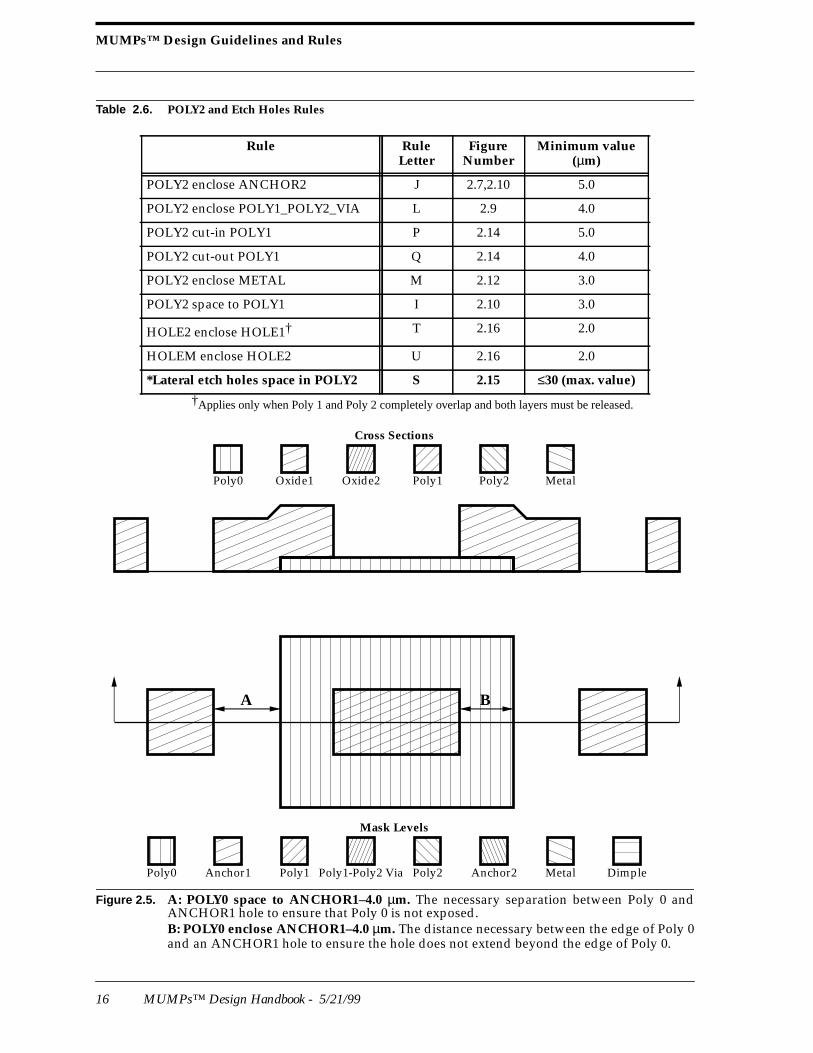
2.2.4 POLY2
Table 2.6 lists the rules that relate to POLY2. Rules J and L ensure that the Poly 2 properly overlapsanchor and via holes. Rules P and Q pertain to proper overlaps of Poly 1 and Poly 2 relative to eachother. Rule M ensures that Metal does not overlap Poly 2. (Users who want extend Metal beyond aPoly 2 pad should be aware that step coverage at the Poly 2 edge is poor and may result in mechanicalfailure and high electrical resistance at the step.) Rule I defines the minimum space between Poly 1and 2 to assure good delineation and avoid shorting. Rule T defines the necessary enclosure of HOLE2around HOLE1 in the special case where Poly 1 and Poly 2 layers overlap and both must be released.Rule U defines the minimum enclosure of HOLEM around HOLE2 to ensure that the holes are prop-erly aligned for release. As with POLY1, the last rule guarantees release of large polysilicon micro-structures.
As mentioned above, rule T applies to the special case where a stack of Poly 1 and Poly 2 must bereleased. To best facilitate release of the structures, etch holes in both layers (HOLE1 and HOLE2)must be aligned and the size of the hole in Poly 2 should exceed the Poly 1 etch hole by 2 µm, i.e.HOLE2 encloses HOLE1 by 2.0 µm.
Rule RuleLetter
FigureNumber
Minimum value(µm)
POLY1 enclose ANCHOR1 G 2.6 4.0
POLY1 enclose DIMPLE N 2.13 4.0
POLY1 enclose POLY1_POLY2_VIA H 2.9, 2.11 4.0
POLY1 enclose POLY2 O 2.14 4.0
POLY1 space to ANCHOR2 K 2.11 3.0
*Lateral etch holes space in POLY1 R 2.15 ≤30 (max. value)
MUMPs™ Design Guidelines and Rules
16 MUMPs™ Design Handbook - 5/21/99
Table 2.6. POLY2 and Etch Holes Rules
†Applies only when Poly 1 and Poly 2 completely overlap and both layers must be released.
Figure 2.5 . A: POLY0 space to ANCHOR1–4.0 µm. The necessary separation between Poly 0 andANCHOR1 hole to ensure that Poly 0 is not exposed.B: POLY0 enclose ANCHOR1–4.0 µm. The distance necessary between the edge of Poly 0and an ANCHOR1 hole to ensure the hole does not extend beyond the edge of Poly 0.
Rule RuleLetter
FigureNumber
Minimum value(µm)
POLY2 enclose ANCHOR2 J 2.7,2.10 5.0
POLY2 enclose POLY1_POLY2_VIA L 2.9 4.0
POLY2 cut-in POLY1 P 2.14 5.0
POLY2 cut-out POLY1 Q 2.14 4.0
POLY2 enclose METAL M 2.12 3.0
POLY2 space to POLY1 I 2.10 3.0
HOLE2 enclose HOLE1† T 2.16 2.0
HOLEM enclose HOLE2 U 2.16 2.0
*Lateral etch holes space in POLY2 S 2.15 ≤30 (max. value)
A B
Poly0 Oxide1 Oxide2 Poly1 Poly2 Metal
Cross Sections
Poly0 Anchor1 Poly1 Poly1-Poly2 Via Poly2 Anchor2 Metal Dimple
Mask Levels
Design Rules
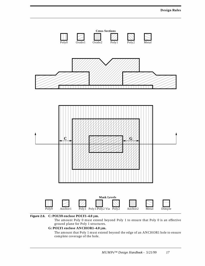
MUMPs™ Design Handbook - 5/21/99 17
Figure 2.6 . C: POLY0 enclose POLY1–4.0 µm.The amount Poly 0 must extend beyond Poly 1 to ensure that Poly 0 is an effectiveground plane for Poly 1 structures.
G: POLY1 enclose ANCHOR1–4.0 µm.The amount that Poly 1 must extend beyond the edge of an ANCHOR1 hole to ensurecomplete coverage of the hole.
C G
Poly0 Oxide1 Oxide2 Poly1 Poly2 Metal
Cross Sections
Poly0 Anchor1 Poly1 Poly1-Poly2 Via Poly2 Anchor2 Metal Dimple
Mask Levels
MUMPs™ Design Guidelines and Rules
18 MUMPs™ Design Handbook - 5/21/99
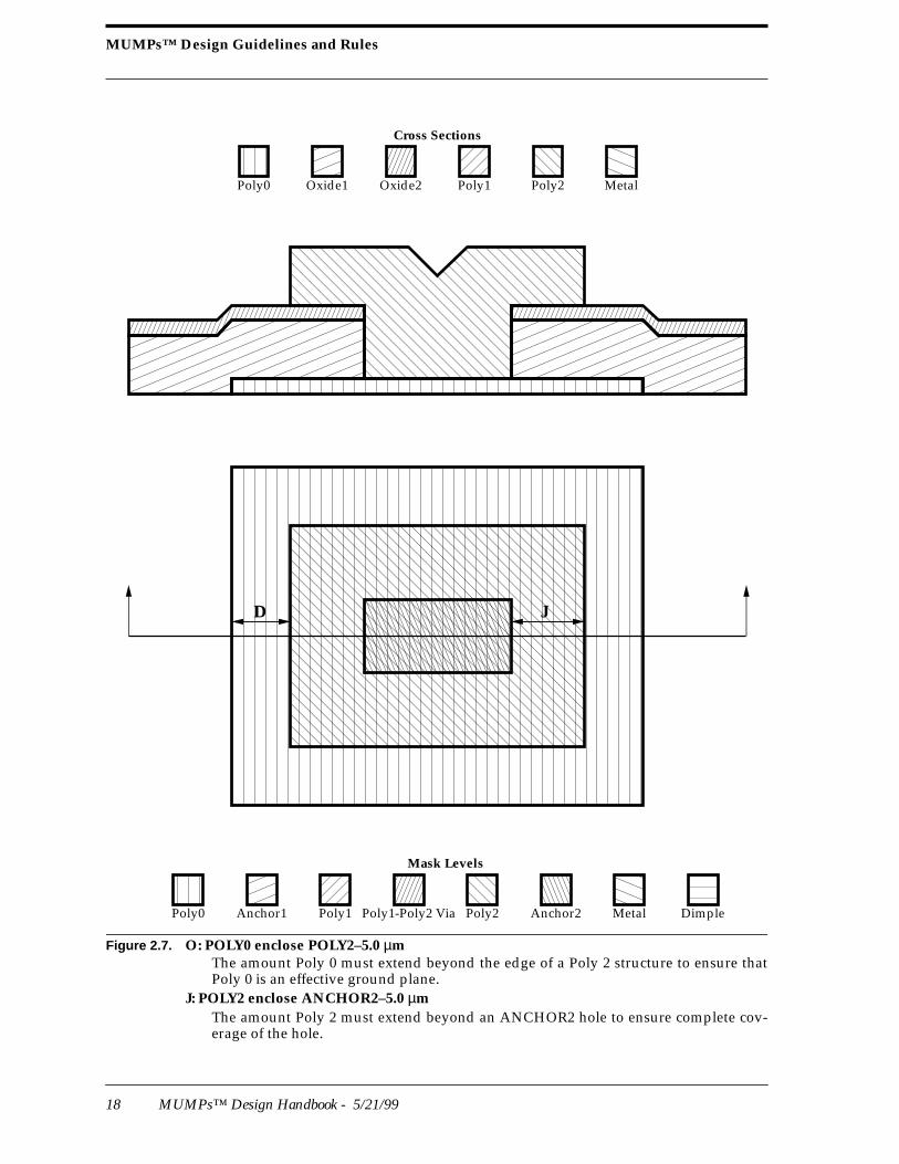
Figure 2.7 . O: POLY0 enclose POLY2–5.0 µmThe amount Poly 0 must extend beyond the edge of a Poly 2 structure to ensure thatPoly 0 is an effective ground plane.
J: POLY2 enclose ANCHOR2–5.0 µmThe amount Poly 2 must extend beyond an ANCHOR2 hole to ensure complete cov-erage of the hole.
Poly0 Oxide1 Oxide2 Poly1 Poly2 Metal
Cross Sections
Poly0 Anchor1 Poly1 Poly1-Poly2 Via Poly2 Anchor2 Metal Dimple
Mask Levels
D J
Design Rules
MUMPs™ Design Handbook - 5/21/99 19
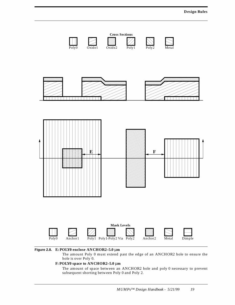
Figure 2.8 . E: POLY0 enclose ANCHOR2–5.0 µmThe amount Poly 0 must extend past the edge of an ANCHOR2 hole to ensure thehole is over Poly 0.
F: POLY0 space to ANCHOR2–5.0 µmThe amount of space between an ANCHOR2 hole and poly 0 necessary to preventsubsequent shorting between Poly 0 and Poly 2.
Poly0 Oxide1 Oxide2 Poly1 Poly2 Metal
Cross Sections
Poly0 Anchor1 Poly1 Poly1-Poly2 Via Poly2 Anchor2 Metal Dimple
Mask Levels
E F
MUMPs™ Design Guidelines and Rules
20 MUMPs™ Design Handbook - 5/21/99
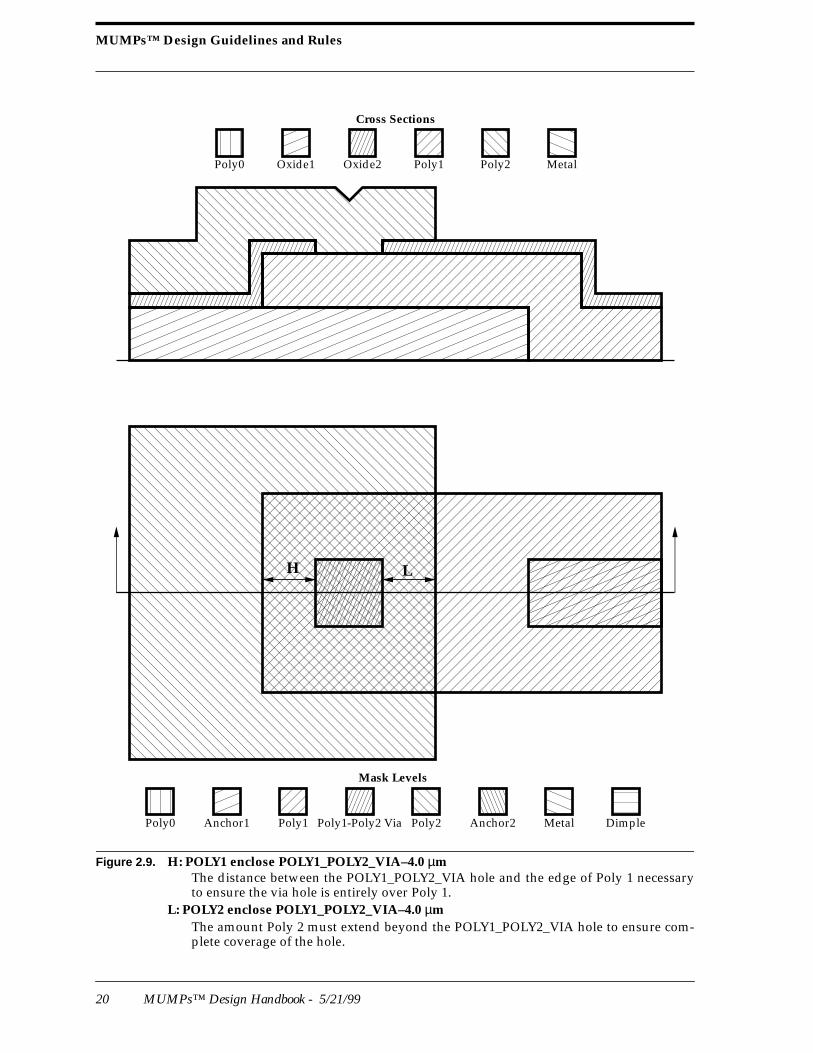
Figure 2.9 . H: POLY1 enclose POLY1_POLY2_VIA–4.0 µmThe distance between the POLY1_POLY2_VIA hole and the edge of Poly 1 necessaryto ensure the via hole is entirely over Poly 1.
L: POLY2 enclose POLY1_POLY2_VIA–4.0 µmThe amount Poly 2 must extend beyond the POLY1_POLY2_VIA hole to ensure com-plete coverage of the hole.
Poly0 Oxide1 Oxide2 Poly1 Poly2 Metal
Cross Sections
Poly0 Anchor1 Poly1 Poly1-Poly2 Via Poly2 Anchor2 Metal Dimple
Mask Levels
H L
Design Rules
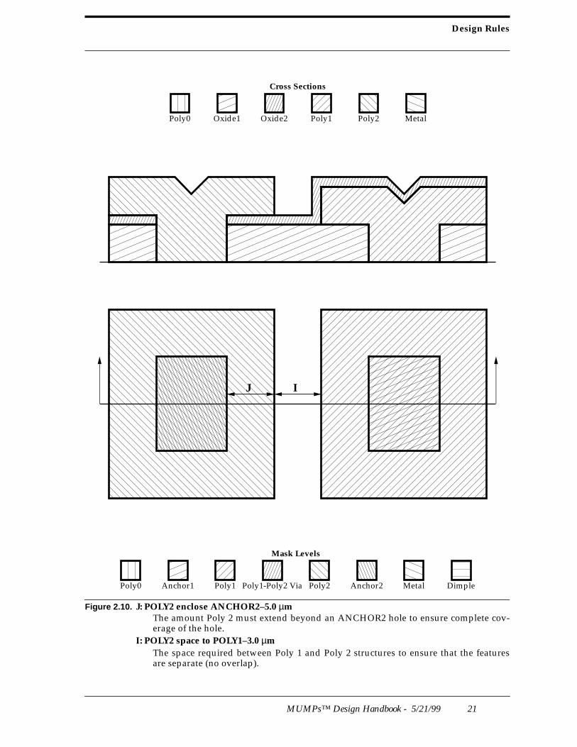
MUMPs™ Design Handbook - 5/21/99 21
Figure 2.10 . J: POLY2 enclose ANCHOR2–5.0 µmThe amount Poly 2 must extend beyond an ANCHOR2 hole to ensure complete cov-erage of the hole.
I: POLY2 space to POLY1–3.0 µmThe space required between Poly 1 and Poly 2 structures to ensure that the featuresare separate (no overlap).
Poly0 Oxide1 Oxide2 Poly1 Poly2 Metal
Cross Sections
Poly0 Anchor1 Poly1 Poly1-Poly2 Via Poly2 Anchor2 Metal Dimple
Mask Levels
IJ
MUMPs™ Design Guidelines and Rules
22 MUMPs™ Design Handbook - 5/21/99
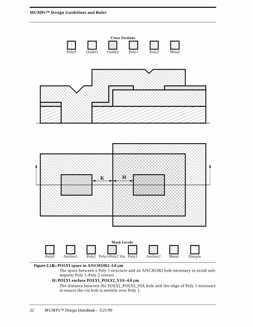
Figure 2.11. K: POLY1 space to ANCHOR2–3.0 µmThe space between a Poly 1 structure and an ANCHOR2 hole necessary to avoid sub-sequent Poly 1–Poly 2 contact.
H: POLY1 enclose POLY1_POLY2_VIA–4.0 µmThe distance between the POLY1_POLY2_VIA hole and the edge of Poly 1 necessaryto ensure the via hole is entirely over Poly 1.
Poly0 Oxide1 Oxide2 Poly1 Poly2 Metal
Cross Sections
Poly0 Anchor1 Poly1 Poly1-Poly2 Via Poly2 Anchor2 Metal Dimple
Mask Levels
HK
Design Rules
MUMPs™ Design Handbook - 5/21/99 23
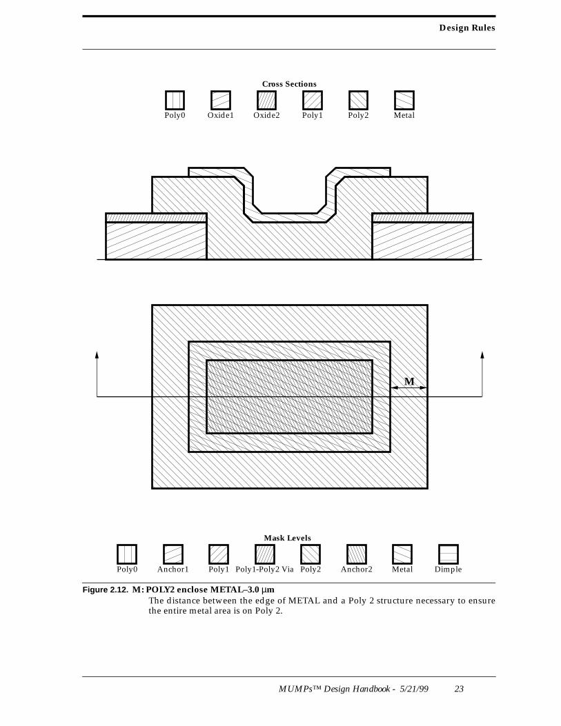
Figure 2.12 . M: POLY2 enclose METAL–3.0 µmThe distance between the edge of METAL and a Poly 2 structure necessary to ensurethe entire metal area is on Poly 2.
Poly0 Oxide1 Oxide2 Poly1 Poly2 Metal
Cross Sections
Poly0 Anchor1 Poly1 Poly1-Poly2 Via Poly2 Anchor2 Metal Dimple
Mask Levels
M
MUMPs™ Design Guidelines and Rules
24 MUMPs™ Design Handbook - 5/21/99
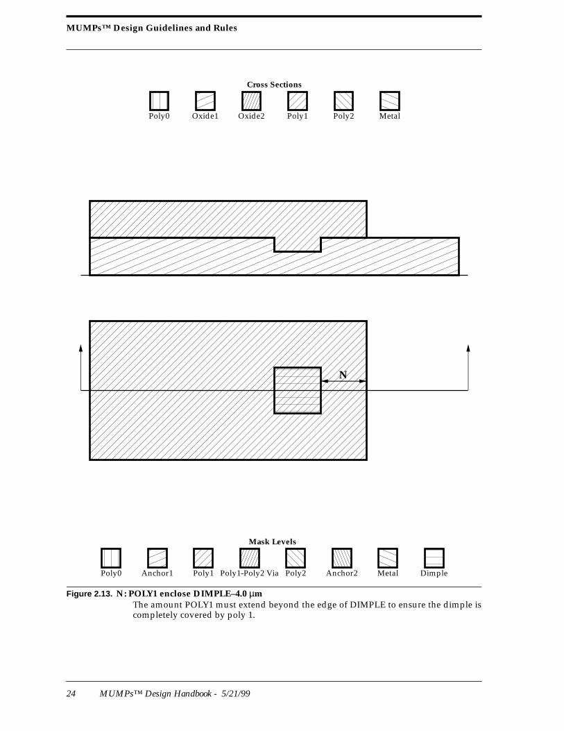
Figure 2.13 . N: POLY1 enclose DIMPLE–4.0 µmThe amount POLY1 must extend beyond the edge of DIMPLE to ensure the dimple iscompletely covered by poly 1.
Poly0 Oxide1 Oxide2 Poly1 Poly2 Metal
Cross Sections
Poly0 Anchor1 Poly1 Poly1-Poly2 Via Poly2 Anchor2 Metal Dimple
Mask Levels
N
Design Rules
MUMPs™ Design Handbook - 5/21/99 25
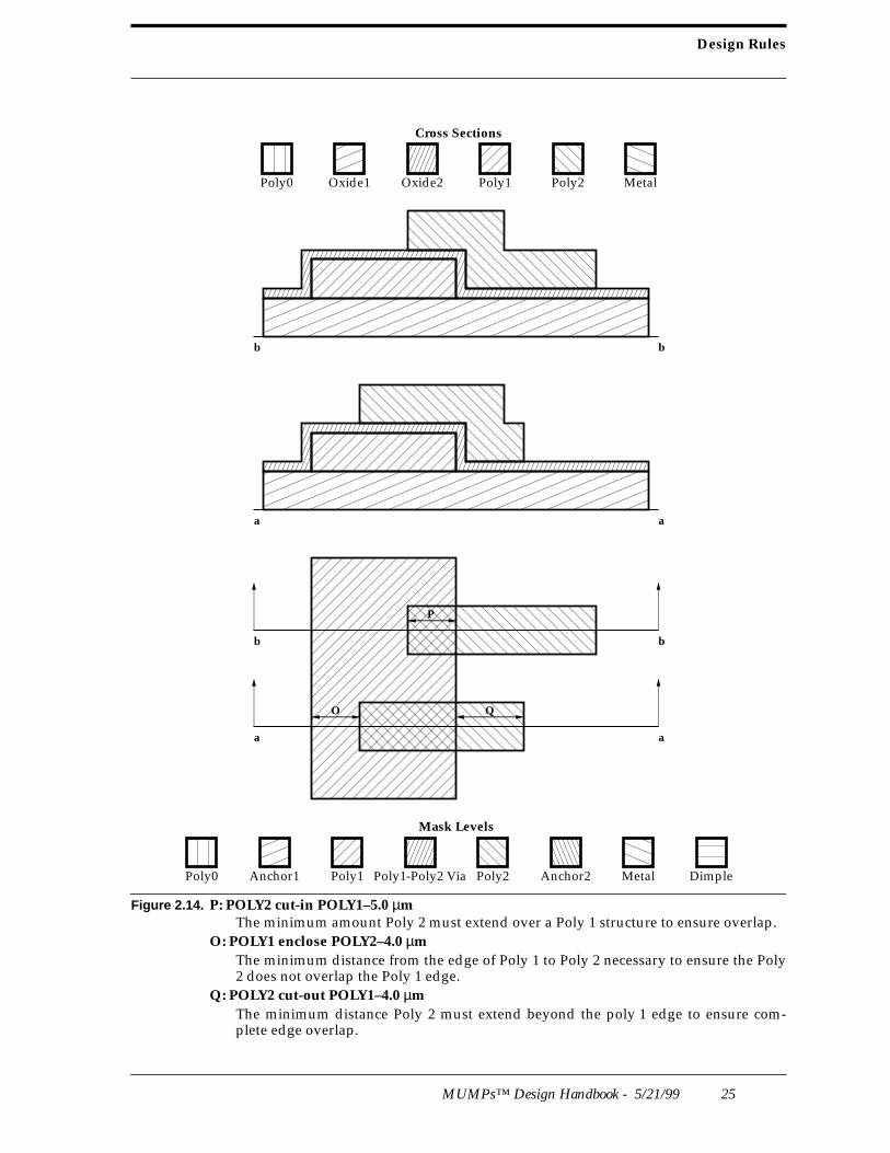
Figure 2.14 . P: POLY2 cut-in POLY1–5.0 µmThe minimum amount Poly 2 must extend over a Poly 1 structure to ensure overlap.
O: POLY1 enclose POLY2–4.0 µmThe minimum distance from the edge of Poly 1 to Poly 2 necessary to ensure the Poly2 does not overlap the Poly 1 edge.
Q: POLY2 cut-out POLY1–4.0 µmThe minimum distance Poly 2 must extend beyond the poly 1 edge to ensure com-plete edge overlap.
Poly0 Oxide1 Oxide2 Poly1 Poly2 Metal
Cross Sections
Poly0 Anchor1 Poly1 Poly1-Poly2 Via Poly2 Anchor2 Metal Dimple
Mask Levels
a a
b b
a a
b b
QO
P
MUMPs™ Design Guidelines and Rules
26 MUMPs™ Design Handbook - 5/21/99
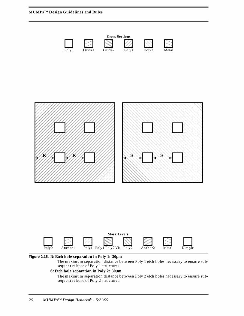
Figure 2.15 . R: Etch hole separation in Poly 1: 30µmThe maximum separation distance between Poly 1 etch holes necessary to ensure sub-sequent release of Poly 1 structures.
S: Etch hole separation in Poly 2: 30µmThe maximum separation distance between Poly 2 etch holes necessary to ensure sub-sequent release of Poly 2 structures.
Poly0 Oxide1 Oxide2 Poly1 Poly2 Metal
Cross Sections
Poly0 Anchor1 Poly1 Poly1-Poly2 Via Poly2 Anchor2 Metal Dimple
Mask Levels
R R S S
Design Rules
MUMPs™ Design Handbook - 5/21/99 27
Figure 2.16 . T: HOLE2 enclose HOLE1–2.0 µmThe necessary border of HOLE2 around HOLE1 to ensure good release results.
U: HOLEM enclose HOLE2–2.0 µmThe necessary border of HOLEM around HOLE2 to ensure good release results.
Poly0 Oxide1 Oxide2 Poly1 Poly2 Metal
Cross Sections
Poly0 Anchor1 Poly1 Poly1-Poly2 Via Poly2 Anchor2 Metal Dimple
Mask Levels
T
U

MUMPs™ Design Guidelines and Rules
28 MUMPs™ Design Handbook - 5/21/99
Tabl
e 2
.7.
Des
ign
ru
le r
efer
ence
sh
eet.
Tab
le s
ho
ws
min
imu
m d
imen
sio
ns
(µm
) (b
old
tex
t), r
ule
nam
e an
d fi
gu
re n
um
ber
, res
pec
tiv
ely.
Lev
el 1
Lev
el 2
Min
imu
mF
eatu
reM
inim
um
Sp
acin
gE
ncl
ose
Sp
acin
gC
ut-
InC
ut-
Ou
t
PO
LY0
-2
2
AN
CH
OR
14/
B/
2.5
4/A
/2.
5
PO
LY1
4/C
/2.
6
AN
CH
OR
25/
E/
2.8
5/F
/2.
8
PO
LY2
5/D
/2.
7
PO
LY1
-2
2
PO
LY0
AN
CH
OR
14/
G/
2.6
AN
CH
OR
23/
K/
2.11
PO
LY2
4/O
/2.
14
DIM
PL
E4/
N/
2.13
PO
LY1_
PO
LY2_
VIA
4/H
/2.
9
PO
LY2
-2
2
PO
LY0
PO
LY1
3/I/
2.10
5/P
/2.
144/
Q/
2.14
VIA
4/L
/2.
9
AN
CH
OR
25/
J/2.
7
ME
TAL
3/M
/2.
12
HO
LE
MH
OL
E2
2/U
/2.
16
HO
LE
2H
OL
E1
2/T
/2.
16
Process and Design Issues (or Hints and Pitfalls)
MUMPs™ Design Handbook - 5/21/99 29
Section 2.3 is highly recommended reading for any MUMPs™ user, novice or experienced. It includesseveral common design errors that warrant extended discussion based on observations from previ-ous MUMPs™ runs. This section also contains guidelines for several processing methods that may beof interest.
2.3 Process and Design Issues (or Hints and Pitfalls)
This section is based upon the experience Cronos has gained working with many groups of people,both novices and experts in the area of MEMS. Below are some of the more common errors made indesigning surface micromachined MEMS along with some helpful hints.
2.3.1 Layout convention
This was covered in section 2.2 but will be reiterated here. The convention used by the MUMPs™ pro-cesses in defining mask levels is simple. For all polysilicon levels and the metal level (POLY0, POLY1,POLY2 and METAL) the masks are light field. For these levels, draw (i.e. digitize) the polysilicon (ormetal) feature you want to keep. All oxide levels and hole levels (DIMPLE, ANCHOR1, ANCHOR2,POLY1_POLY2_VIA and HOLE0,1,2,M) are dark field. For these levels, draw the hole you want tomake. It is imperative that these conventions be followed for your devices to be fabricated correctly.
2.3.2 Don’t put a hole where you don’t need it.
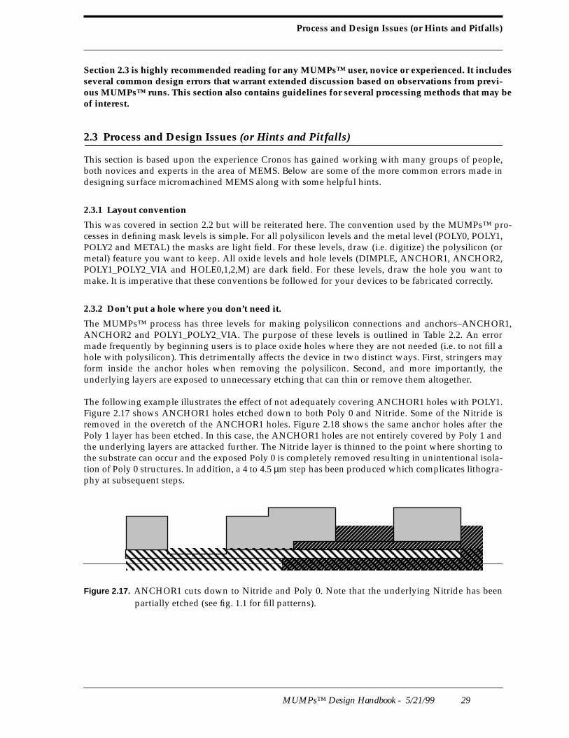
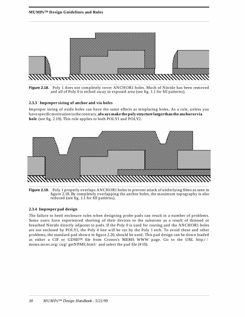
The MUMPs™ process has three levels for making polysilicon connections and anchors–ANCHOR1,ANCHOR2 and POLY1_POLY2_VIA. The purpose of these levels is outlined in Table 2.2. An errormade frequently by beginning users is to place oxide holes where they are not needed (i.e. to not fill ahole with polysilicon). This detrimentally affects the device in two distinct ways. First, stringers mayform inside the anchor holes when removing the polysilicon. Second, and more importantly, theunderlying layers are exposed to unnecessary etching that can thin or remove them altogether.
The following example illustrates the effect of not adequately covering ANCHOR1 holes with POLY1.Figure 2.17 shows ANCHOR1 holes etched down to both Poly 0 and Nitride. Some of the Nitride isremoved in the overetch of the ANCHOR1 holes. Figure 2.18 shows the same anchor holes after thePoly 1 layer has been etched. In this case, the ANCHOR1 holes are not entirely covered by Poly 1 andthe underlying layers are attacked further. The Nitride layer is thinned to the point where shorting tothe substrate can occur and the exposed Poly 0 is completely removed resulting in unintentional isola-tion of Poly 0 structures. In addition, a 4 to 4.5 µm step has been produced which complicates lithogra-phy at subsequent steps.
Figure 2.17 . ANCHOR1 cuts down to Nitride and Poly 0. Note that the underlying Nitride has beenpartially etched (see fig. 1.1 for fill patterns).
AAAAAAAAAAAAAAAAAA
AAAAAAAAAAAAAAAA
MUMPs™ Design Guidelines and Rules
30 MUMPs™ Design Handbook - 5/21/99
Figure 2.18. Poly 1 does not completely cover ANCHOR1 holes. Much of Nitride has been removedand all of Poly 0 is etched away in exposed area (see fig. 1.1 for fill patterns).
2.3.3 Improper sizing of anchor and via holes
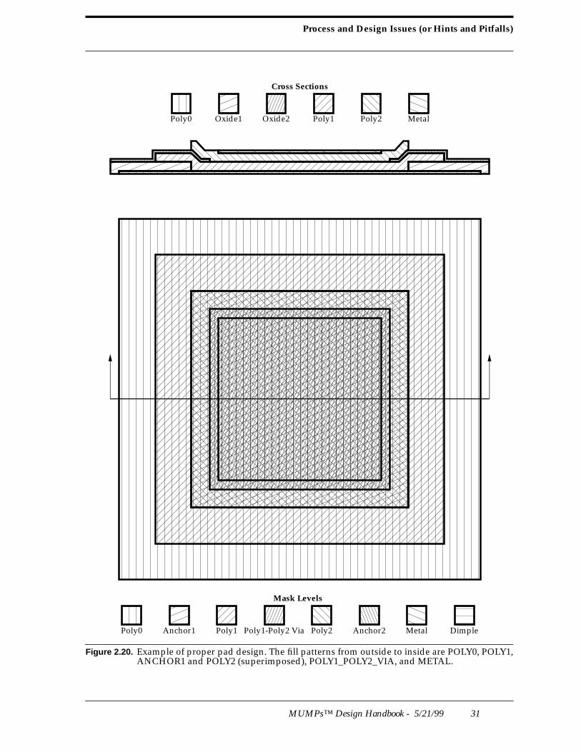
Improper sizing of oxide holes can have the same effects as misplacing holes. As a rule, unless youhave specific motivation to the contrary, always make the poly structure larger than the anchor or viahole (see fig. 2.19). This rule applies to both POLY1 and POLY2.
Figure 2.19. Poly 1 properly overlaps ANCHOR1 holes to prevent attack of underlying films as seen infigure 2.18. By completely overlapping the anchor holes, the maximum topography is alsoreduced (see fig. 1.1 for fill patterns).
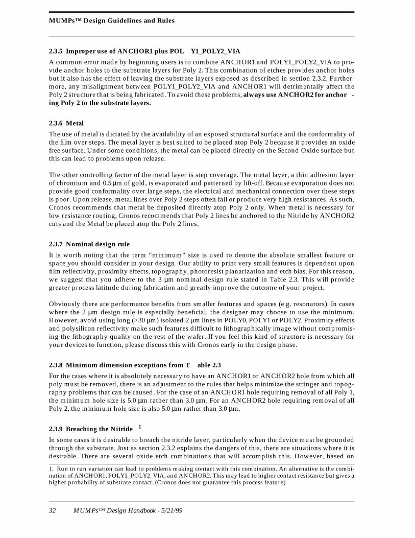
2.3.4 Improper pad design
The failure to heed enclosure rules when designing probe pads can result in a number of problems.Some users have experienced shorting of their devices to the substrate as a result of thinned orbreached Nitride directly adjacent to pads. If the Poly 0 is used for routing and the ANCHOR1 holesare not enclosed by POLY1, the Poly 0 line will be cut by the Poly 1 etch. To avoid these and otherproblems, the standard pad shown in figure 2.20, should be used. This pad design can be down loadedas either a CIF or GDSII™ file from Cronos's MEMS WWW page. Go to the URL http://mems.mcnc.org/cug/getNPME.html/ and select the pad file (#10).
Process and Design Issues (or Hints and Pitfalls)
MUMPs™ Design Handbook - 5/21/99 31
Figure 2.20 . Example of proper pad design. The fill patterns from outside to inside are POLY0, POLY1,ANCHOR1 and POLY2 (superimposed), POLY1_POLY2_VIA, and METAL.
Poly0 Oxide1 Oxide2 Poly1 Poly2 Metal
Cross Sections
Poly0 Anchor1 Poly1 Poly1-Poly2 Via Poly2 Anchor2 Metal Dimple
Mask Levels
MUMPs™ Design Guidelines and Rules
32 MUMPs™ Design Handbook - 5/21/99
2.3.5 Improper use of ANCHOR1 plus POL Y1_POLY2_VIA
A common error made by beginning users is to combine ANCHOR1 and POLY1_POLY2_VIA to pro-vide anchor holes to the substrate layers for Poly 2. This combination of etches provides anchor holesbut it also has the effect of leaving the substrate layers exposed as described in section 2.3.2. Further-more, any misalignment between POLY1_POLY2_VIA and ANCHOR1 will detrimentally affect thePoly 2 structure that is being fabricated. To avoid these problems, always use ANCHOR2 for anchor -ing Poly 2 to the substrate layers.
2.3.6 Metal
The use of metal is dictated by the availability of an exposed structural surface and the conformality ofthe film over steps. The metal layer is best suited to be placed atop Poly 2 because it provides an oxidefree surface. Under some conditions, the metal can be placed directly on the Second Oxide surface butthis can lead to problems upon release.
The other controlling factor of the metal layer is step coverage. The metal layer, a thin adhesion layerof chromium and 0.5 µm of gold, is evaporated and patterned by lift-off. Because evaporation does notprovide good conformality over large steps, the electrical and mechanical connection over these stepsis poor. Upon release, metal lines over Poly 2 steps often fail or produce very high resistances. As such,Cronos recommends that metal be deposited directly atop Poly 2 only. When metal is necessary forlow resistance routing, Cronos recommends that Poly 2 lines be anchored to the Nitride by ANCHOR2cuts and the Metal be placed atop the Poly 2 lines.
2.3.7 Nominal design rule
It is worth noting that the term “minimum” size is used to denote the absolute smallest feature orspace you should consider in your design. Our ability to print very small features is dependent uponfilm reflectivity, proximity effects, topography, photoresist planarization and etch bias. For this reason,we suggest that you adhere to the 3 µm nominal design rule stated in Table 2.3. This will providegreater process latitude during fabrication and greatly improve the outcome of your project.
Obviously there are performance benefits from smaller features and spaces (e.g. resonators). In caseswhere the 2 µm design rule is especially beneficial, the designer may choose to use the minimum.However, avoid using long (>30 µm) isolated 2 µm lines in POLY0, POLY1 or POLY2. Proximity effectsand polysilicon reflectivity make such features difficult to lithographically image without compromis-ing the lithography quality on the rest of the wafer. If you feel this kind of structure is necessary foryour devices to function, please discuss this with Cronos early in the design phase.
2.3.8 Minimum dimension exceptions from T able 2.3
For the cases where it is absolutely necessary to have an ANCHOR1 or ANCHOR2 hole from which allpoly must be removed, there is an adjustment to the rules that helps minimize the stringer and topog-raphy problems that can be caused. For the case of an ANCHOR1 hole requiring removal of all Poly 1,the minimum hole size is 5.0 µm rather than 3.0 µm. For an ANCHOR2 hole requiring removal of allPoly 2, the minimum hole size is also 5.0 µm rather than 3.0 µm.
2.3.9 Breaching the Nitride 1
In some cases it is desirable to breach the nitride layer, particularly when the device must be groundedthrough the substrate. Just as section 2.3.2 explains the dangers of this, there are situations where it isdesirable. There are several oxide etch combinations that will accomplish this. However, based on
1. Run to run variation can lead to problems making contact with this combination. An alternative is the combi-nation of ANCHOR1, POLY1_POLY2_VIA, and ANCHOR2. This may lead to higher contact resistance but gives ahigher probability of substrate contact. (Cronos does not guarantee this process feature)
Film Parameters
MUMPs™ Design Handbook - 5/21/99 33
empirical results, the optimum combination (i.e. lowest contact resistance) is ANCHOR1 plusPOLY1_POLY2_VIA (and removing the Poly 1). The anchor hole can then be filled with Poly 2 to pro-vide a ground to substrate connection.
This is not a guaranteed process.
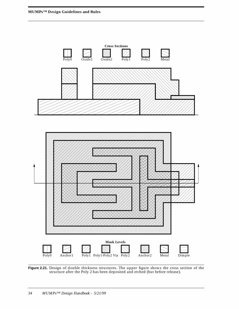
2.3.10 Creating Double Thickness Structures
Over past MUMPs™ runs, a technique has been developed for producing polysilicon parts made of bothPoly1 and 21. The advantage of this technique is that the final stacked structure is indistinguishablefrom a device made from a single 3.5 µm polysilicon film. Figure 2.21 shows an example of how to fab-ricate the double thickness structure. The technique is based on the fact that the overetch of the Poly 2etch is sufficient to completely etch an underlying Poly 1 layer. In this way, both films are etched usingthe same mask. The process is as follows:
1. Draw a continuous sheet in POLY1.2. Draw a continuous POLY1_POLY2_VIA that encloses POLY1 by 5 µm.3. Draw the POLY2 structure over the POLY1 sheet to the desired pattern.
In cases where POLY1 leads are drawn from the structure, it is essential that the POLY2 extend beyondthe POLY1_POLY2_VIA cut by a minimum of 3.0 µm. If the POLY2 does not extend beyond the viahole, the POLY1 will be truncated and the structure will be electrically isolated.
This is not a guaranteed process.
2.4 Film Parameters
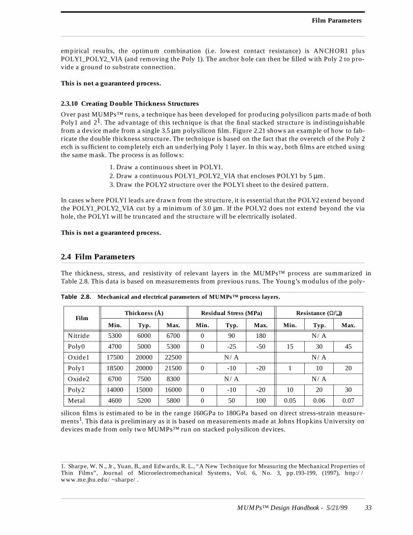
The thickness, stress, and resistivity of relevant layers in the MUMPs™ process are summarized inTable 2.8. This data is based on measurements from previous runs. The Young’s modulus of the poly-
silicon films is estimated to be in the range 160GPa to 180GPa based on direct stress-strain measure-ments1. This data is preliminary as it is based on measurements made at Johns Hopkins University ondevices made from only two MUMPs™ run on stacked polysilicon devices.
1. Sharpe, W. N., Jr., Yuan, B., and Edwards, R. L., “A New Technique for Measuring the Mechanical Properties ofThin Films”, Journal of Microelectromechanical Systems, Vol. 6, No. 3, pp.193-199, (1997), http://www.me.jhu.edu/~sharpe/.
Table 2.8. Mechanical and electrical parameters of MUMPs™ process layers.
FilmThickness (Å) Residual Stress (MPa) Resistance (Ω/)
Min. Typ. Max. Min. Typ. Max. Min. Typ. Max.
Nitride 5300 6000 6700 0 90 180 N/A
Poly0 4700 5000 5300 0 -25 -50 15 30 45
Oxide1 17500 20000 22500 N/A N/A
Poly1 18500 20000 21500 0 -10 -20 1 10 20
Oxide2 6700 7500 8300 N/A N/A
Poly2 14000 15000 16000 0 -10 -20 10 20 30
Metal 4600 5200 5800 0 50 100 0.05 0.06 0.07
MUMPs™ Design Guidelines and Rules
34 MUMPs™ Design Handbook - 5/21/99
Figure 2.21 . Design of double thickness structures. The upper figure shows the cross section of thestructure after the Poly 2 has been deposited and etched (but before release).
Poly0 Oxide1 Oxide2 Poly1 Poly2 Metal
Cross Sections
Poly0 Anchor1 Poly1 Poly1-Poly2 Via Poly2 Anchor2 Metal Dimple
Mask Levels
EZ-MUMPs™ Design Rules
MUMPs™ Design Handbook - 5/21/99 35
2.5 EZ-MUMPs™ Design Rules
For those participants inexperienced in the intricacies of process-design, rule interactions, or eventhose who are experienced but who really don’t need to push the design envelope for their designs, werecommend the EZ-MUMPs™ rules. If you make all minimum geometries ≥ 5.0 µm (lines and spaces),and all overlaps and borders ≥ 5.0 µm, you will easily meet all the aforementioned design rules andyou minimize any potential process-design interactions. (Please note that the etch hole spacings, rulesR and S, must still be ≤ 30.0 µm).
2.6 Layout Requirements
2.6.1 Usable Area
The maximum allowed design area for MUMPs™ is 1cm x 1cm. Care should be taken to avoid placingstructures closer than 100µm from the edge of the die since dicing can occasionally damage the edge ofthe chip. It is required that you leave the 550µm x 300 µm (x and y dimensions, respectively) rectan-gle vacant in the lower left hand corner of your die. This space is used by Cronos for a drop in teststructure for post process evaluation of the run.
2.6.2 Cell Name Restrictions
Some errors have occurred in the past due to nonstandard cell names. In order to reduce these errorsand the time it takes to translate designs, some guidelines need to be put in place. They are as follows:
• Cell names should be under 28 characters.
• Cell names should consist of only the following characters or numerals [a-zA-Z0-9] and the underscore character ‘_’.
2.6.3 Layer Names
Layouts must use layer names as indicated in Table 2.3. For CIF submissions the indicated namesshould be used (i.e. for POLY0 use CPZ) and for GDS submissions the correct number must be used.Other layers may be in the design; but, they will be ignored. For TDB submissions the GDS numbersand CIF layer names should be assigned correctly. Cronos is not responsible for layers omitted due tofailure to comply to naming conventions.
2.6.4 General Layout Tips
Cadence software is currently used to assemble the MUMPs™ wafers. It does a reasonable job with mosttranslations; however, there are some additional nuances of which users should be aware.
• Non-orthogonal rotations are not translated correctly. This causes objectionable cells to be flagged and then flattened usually in Tanner’s L-Edit. A minor addendum to this note is that GDS files output from L-Edit with non-orthogonal rotation and mirroring of a cell are incor-rect in versions of L-Edit before version 8. So when reading files into version 8 make a special check for these occurrences. Cronos currently uses version 6 of L-Edit to flatten these instances before they are read into Cadence.
• In GDS, three wire types are allowed, extended, butted, and rounded ends. Rounded ended wires will be converted to an octagon ending. It is strongly suggested that only extended wire types be used with cif files; otherwise, information may be lost and connections bro-ken.
MUMPs™ Design Guidelines and Rules
36 MUMPs™ Design Handbook - 5/21/99
2.6.5 Design Rule Checking
PLEASE NOTE THAT NO ERROR CHECKING WILL BE DONE ON YOUR DESIGN. Design rule check-ing files are also located at our anonymous ftp site as follows:
ftp.mcnc.org:/ftp/pub/MEMS/TANNER/mpmems.tdbftp.mcnc.org:/ftp/pub/MEMS/CADENCE/mumps.dracftp.mcnc.org:/ftp/pub/MEMS/CADENCE/mumps13.drc.tfftp.mcnc.org:/ftp/pub/MEMS/Mentor/mumps.rules.
2.7 Layout Submission
Please submit designs in GDSII™ format. CIF and TBD, version 6 only , formats can also be accepted ifGDS is producing errors or is unavailable. DXF (Autocad™) formatted files are subject to an addi-tional fee for conversion and the files must be submitted at least one week prior to the design deadline.The fee for DXF conversion is $150/hour with a minimum 3 hour charge ($450). Some rules to help layout with mechanical cad tools are located in the directory
ftp.mcnc.org:/ftp/pub/MEMS/AUTOCAD
Additionally, for DXF submissions please use the CIF naming convention as given in Table 2.3.
Technology files are available for L-Edit™, Cadence™, Magic™ and Mentor’s layout tool. The follow-ing are ftp paths for these files:
ftp.mcnc.org:/ftp/pub/MEMS/TANNER/mpmems.tdbftp.mcnc.org:/ftp/pub/MEMS/CADENCE/mumps.tfftp.mcnc.org:/ftp/pub/MEMS/MAGIC/READMEftp.mcnc.org:/ftp/pub/MEMS/Mentor/MUMPS.icproc_12 andMUMPS.Ic_persist_process.attr
A design may be submitted via either FTP or email The ftp site is write only. In either case, please sendthe completed MUMPs™ design submission form at http://mems.mcnc.org/desinfo.html. Designs aredue to Cronos by 24:00 EST on the day of the deadline.
To submit your design by FTP, use the following procedure:
ftp ftp.mcnc.orgName: anonymousPassword: your loginftp> cd pub/incomingftp> type binaryftp> put yourfilenameftp> quit
Example: Bill (login: [email protected]) submits his run#13 design called design.example.
ftp ftp.mcnc.orgName: anonymousPassword: [email protected]> cd pub/incomingftp> type binaryftp> put design.exampleftp> quit

Custom Dicing, Releasing and Critical Point Drying
MUMPs™ Design Handbook - 5/21/99 37
To submit your design by email, either attach it to your email or use the following procedure:
For TBD and GDSII™:uuencode filename filename > filename.uumail [email protected] < filename.uu
2.8 Custom Dicing, Releasing and Critical Point Drying
Cronos offers limited dicing, releasing and supercritical CO2 drying service to MUMPs™ customers. Inorder to provide the best possible service, a set of rules has been established.
2.8.1 Dicing
The minimum size of a subdiced MUMPs™ chip is 2.5 mm. This allows users to dice a single 1 cm x 1 cmdie into 16 sub chips. Any combination of cuts larger than 2.5 mm is acceptable but all cuts must beorthogonal and the 1 cm long. Dicing streets must be provided. Streets should be drawn in POLY0 andmust be 150 µm wide. Releasing of subdiced MUMPs™ chips is subject to additional cost beyond theadvertised $250 due to the added complexity of handling.
2.8.2 HF Release and Supercritical CO2 Drying
Cronos will perform a standard HF release designed to fully remove the sacrificial oxide from chipsthat have been designed with the proper etch hole spacing. This process will not be performed onchips less than 5 mm in size. The cost of HF release is $250/15 (sub)chips. For example, a single diesite subdiced into a 2x2 array costs 4x$250=$1000 to release.
Stiction of released devices is a common problem. One way to minimize this effect is to dry the chipsafter HF release by critical point drying in CO2. Cronos provides this service at a cost of $525/15 chips.