modeling and simulation of free space optoelectronic systems timothy p. kurzweg jose a. martinez...
TRANSCRIPT
Modeling and Simulation of Free Space Optoelectronic Systems
• Timothy P. Kurzweg• Jose A. Martinez • Steven P. Levitan• Donald M. Chiarulli
University of Pittsburgh
• Philippe J. Marchand• Susant Patra• Lee Hendrick• Xuezhe Zheng
University of California San Diego
Funding DARPA: F30602-97-2-0122 / NSF: ECS 96-16879
What’s the Problem
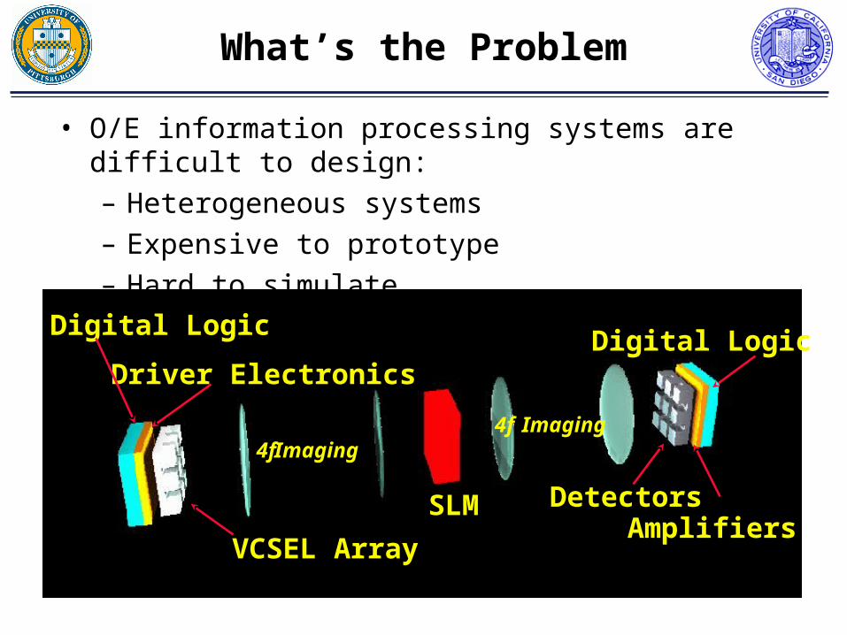
• O/E information processing systems are difficult to design:
– Heterogeneous systems
– Expensive to prototype
– Hard to simulate
SLM
4f Imaging4f Imaging
Detectors
Driver Electronics
VCSEL Array
Digital LogicDigital Logic
Amplifiers
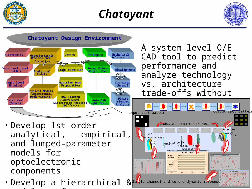
Chatoyant
Chatoyant Design Environment
Electronics Optics Packaging MechanicalTolerancing
Functional level(VHDL)
Logic level(GateSim)
Gate level(Spice)
Devices andCircuits
AnalyticalModels
Physical Models(Experimental
Data fitting)
Image Formation
Gaussian BeamPropagation
Ray Tracing(CodeV,Zemax)
Diffraction Analysis(Diffract)
Misalignment
1st orderthermal
FiniteElementAnalysis
Area, VolumeWeight, Cost
Auto-CADLight Tools
Optoelectronic
A system level O/E CAD tool to predict performance and analyze technology vs. architecture trade-offs without costly prototyping
• Develop 1st order analytical, empirical, and lumped-parameter models for optoelectronic components
• Develop a hierarchical & modular software environment using Ptolemy engine
input spot pattern output spot pattern
VCSEL source array
optical pathSpatial light
modulator
Gaussian beam cross sections
Detectorarray
Single channel end-to-end dynamic response
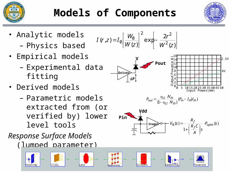
Models of Components
• Analytic models
– Physics based
• Empirical models
– Experimental datafitting
• Derived models
– Parametric models extracted from (or verified by) lower level tools
Response Surface Models(lumped parameter)
0246810121416
0 5 10 15 20 25 30 35 40 45 50
Ou
tpu
t P
ow
er( m
W)
Input Power(mW)
2.5V
4V
V
Driver
P
Pout
)()/1(
/ththin
thLI
thLIout VIP
V
VP
Vdd
PinStage1 )(
1
)(0 sP
sA
CR
RsV optic
f
f
)(
2exp
)(),(
2
220
0zW
rzW
WIzrI
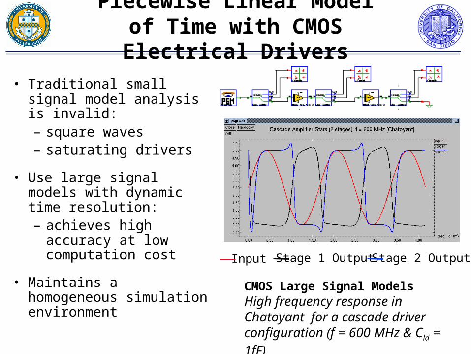
• Traditional small signal model analysis is invalid:– square waves– saturating drivers
• Use large signal models with dynamic time resolution:– achieves high accuracy at
low computation cost
• Maintains a homogeneous simulation environment
Piecewise Linear Model of Time with CMOS Electrical Drivers
CMOS Large Signal ModelsHigh frequency response in Chatoyant for a cascade driver configuration (f = 600 MHz & Cld = 1fF).
Input Stage 1 Output Stage 2 Output
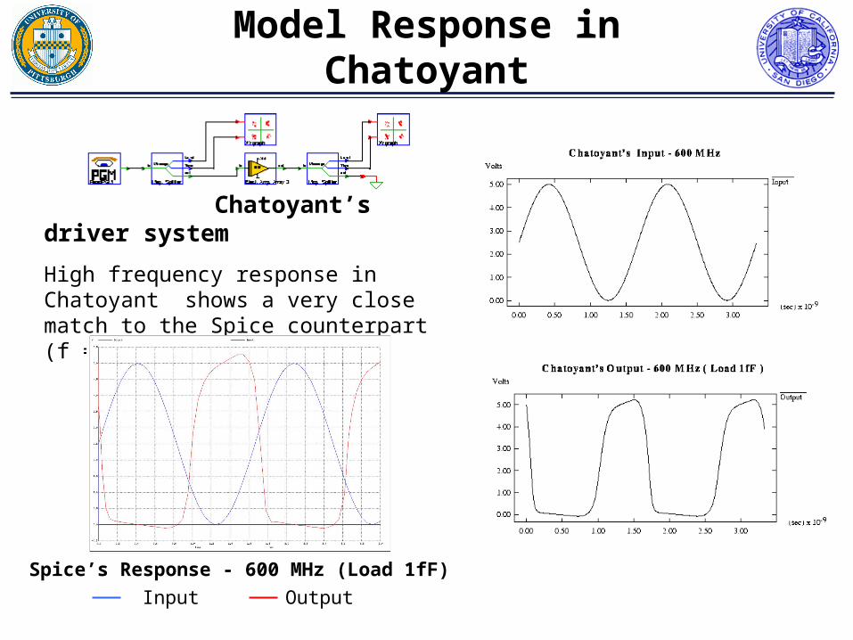
Model Response in Chatoyant
Chatoyant’s driver system
High frequency response in Chatoyant shows a very close match to the Spice counterpart (f = 600 MHz & Cld = 1fF).
Spice’s Response - 600 MHz (Load 1fF)
Input Output
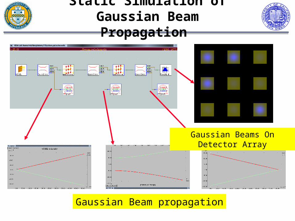
Gaussian Beam propagation
Static Simulation of Gaussian Beam Propagation
Gaussian Beams On Detector Array
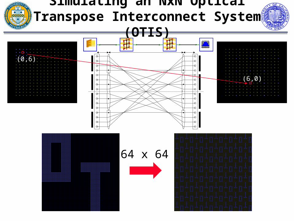
Simulating an NxN Optical Transpose Interconnect System (OTIS)
(0,6)
(6,0)
64 x 64
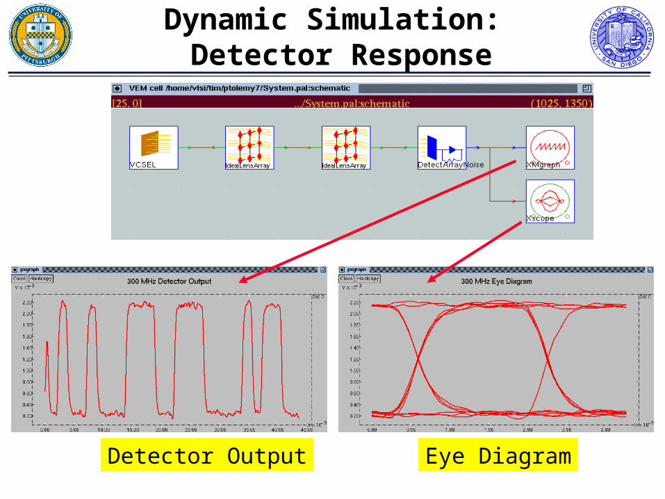
Dynamic Simulation: Detector Response
Detector Output Eye Diagram
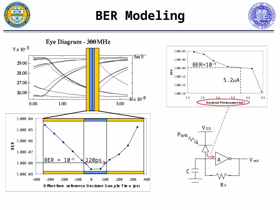
BER Modeling
1.00E-18
1.00E-15
1.00E-12
1.00E-09
1.00E-06
1.00E-03
1.5 2.5 3.5 4.5 5.5 6.5
Recieved Photocurrent (uA)
BE
R1.00E-09
1.00E-08
1.00E-07
1.00E-06
1.00E-05
1.00E-04
-400 -300 -200 -100 0 100 200 300 400
Offset from reference Decision Sample Time (ps)
BE
R
BER = 10-9 120ps
Poptic
VDD
C
A
Rf
Vout
BER=10-9
5.2A
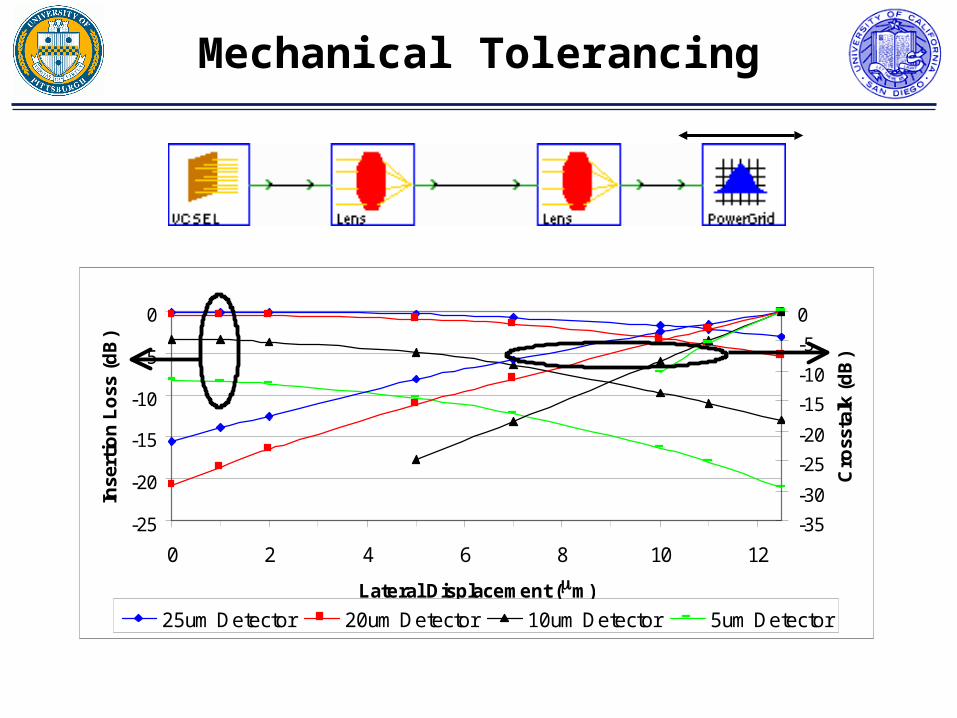
Mechanical Tolerancing
-25
-20
-15
-10
-5
0
0 2 4 6 8 10 12
Lateral Displacement (m)
Inse
rtio
n L
oss
(d
B)
-35
-30
-25
-20
-15
-10
-5
0
Cro
ssta
lk (
dB
)
25um Detector 20um Detector 10um Detector 5um Detector
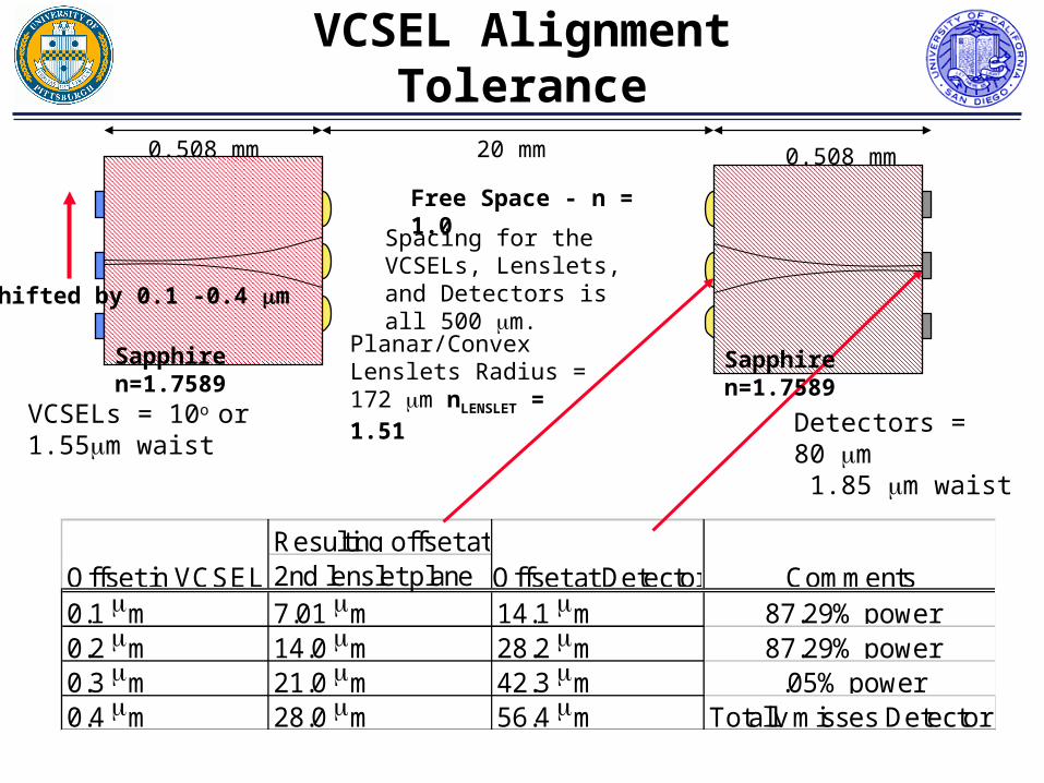
VCSEL Alignment Tolerance
0.508 mm 0.508 mm20 mm
VCSELs = 10o or 1.55m waist
Detectors = 80 m 1.85 m waist
Shifted by 0.1 -0.4 m
Resulting offset at 2nd lenslet plane
0.1 m 7.01 m 14.1 m 87.29% power0.2 m 14.0 m 28.2 m 87.29% power0.3 m 21.0 m 42.3 m .05% power0.4 m 28.0 m 56.4 m Totally misses Detector
CommentsOffset in VCSEL Offset at Detector
Planar/Convex Lenslets Radius = 172 m nLENSLET = 1.51
Free Space - n = 1.0
Spacing for the VCSELs, Lenslets, and Detectors is all 500 m.
Sapphire n=1.7589 Sapphire n=1.7589
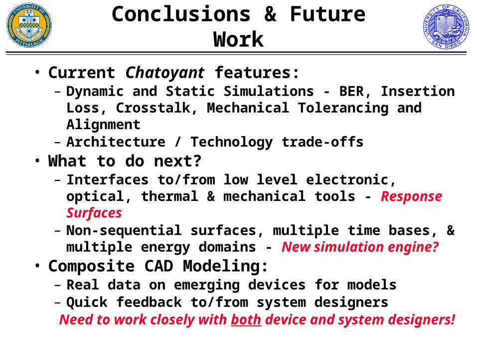
Conclusions & Future Work
• Current Chatoyant features: – Dynamic and Static Simulations - BER, Insertion Loss,
Crosstalk, Mechanical Tolerancing and Alignment– Architecture / Technology trade-offs
• What to do next?– Interfaces to/from low level electronic, optical, thermal
& mechanical tools - Response Surfaces– Non-sequential surfaces, multiple time bases, & multiple
energy domains - New simulation engine?• Composite CAD Modeling:
– Real data on emerging devices for models– Quick feedback to/from system designersNeed to work closely with both device and system designers!