minority carrier lifetime in silicon photovoltaics the effect of
TRANSCRIPT

http://wrap.warwick.ac.uk
Original citation: Murphy, J. D. (John D.), McGuire, R. E., Bothe, Karsten, Voronkov, V. V. and Falster, Robert J.. (2014) Minority carrier lifetime in silicon photovoltaics : the effect of oxygen precipitation. Solar Energy Materials and Solar Cells, Volume 120 (Part A). pp. 402-411. ISSN 0927-0248 Permanent WRAP url: http://wrap.warwick.ac.uk/55873 Copyright and reuse: The Warwick Research Archive Portal (WRAP) makes this work of researchers of the University of Warwick available open access under the following conditions. This article is made available under the Creative Commons Attribution 3.0 (CC BY 3.0) license and may be reused according to the conditions of the license. For more details see: http://creativecommons.org/licenses/by/3.0/ A note on versions: The version presented in WRAP is the published version, or, version of record, and may be cited as it appears here. For more information, please contact the WRAP Team at: [email protected]

Solar Energy Materials & Solar Cells 120 (2014) 402–411
Contents lists available at ScienceDirect
Solar Energy Materials & Solar Cells
0927-02http://d
☆ThisCommoreprodu
n CorrE-m
journal homepage: www.elsevier.com/locate/solmat
Minority carrier lifetime in silicon photovoltaics: The effect ofoxygen precipitation$
J.D. Murphy a,n, R.E. McGuire b, K. Bothe c, V.V. Voronkov d, R.J. Falster d
a University of Warwick, WMG, International Manufacturing Centre, Coventry, CV4 7AL, UKb University of Oxford, Department of Materials, Parks Road, Oxford, OX1 3PH, UKc Institut für Solarenergieforschung Hameln/Emmerthal, Am Ohrberg 1, 31860 Emmerthal, Germanyd SunEdison, viale Gherzi 31, 28100 Novara, Italy
a r t i c l e i n f o
Available online 15 July 2013
Keywords:SiliconPhotovoltaicOxide precipitateLifetimeRecombination
48/$ - see front matter & 2013 The Authors. Px.doi.org/10.1016/j.solmat.2013.06.018
is an open-access article distributed undens Attribution License, which permits unresction in any medium, provided the original auesponding author. Tel.: +44 24 7657 5378.ail address: [email protected] (J.D
a b s t r a c t
Single-crystal Czochralski silicon used for photovoltaics is typically supersaturated with interstitialoxygen at temperatures just below the melting point. Oxide precipitates therefore can form during ingotcooling and cell processing, and nucleation sites are typically vacancy-rich regions. Oxygen precipitationgives rise to recombination centres, which can reduce cell efficiencies by as much as 4% (absolute). Wehave studied the recombination behaviour in p-type and n-type monocrystalline silicon with a range ofdoping levels intentionally processed to contain oxide precipitates with a range of densities, sizes andmorphologies. We analyse injection-dependent minority carrier lifetime measurements to give a fullparameterisation of the recombination activity in terms of Shockley–Read–Hall statistics. We intention-ally contaminate specimens with iron, and show recombination activity arises from iron segregated tooxide precipitates and surrounding defects. We find that phosphorus diffusion gettering reduces therecombination activity of the precipitates to some extent. We also find that bulk iron is preferentiallygettered to the phosphorus diffused layer rather than to oxide precipitates.
& 2013 The Authors. Published by Elsevier B.V. All rights reserved.
1. Introduction
At present the majority of solar cells are made from bulkcrystalline silicon. Minority carrier lifetime is the main parameterused to assess the quality of wafers fromwhich cells are produced.For a given generation rate, the minority carrier lifetime is largelydetermined by recombination processes. Some recombination isintrinsic (band-to-band and Auger), while other is determined bydefects in the bulk or at surfaces. It is necessary to understandwhich defects are typically present in solar wafers before proces-sing, and what effect processing has on those defects. Moreover, itis important to understand the mechanism by which the relevantdefects give rise to recombination, as well as to quantify theirrecombination activity.
Monocrystalline Czochralski silicon (Cz-Si) typically contains�1018 cm−3 of interstitial oxygen, which is mainly incorporatedfrom the silica crucible which contains the melt. This level ofoxygen is supersaturated below ∼1200 1C, so the equilibrium state
ublished by Elsevier B.V. All rights
r the terms of the Creativetricted use, distribution, andthor and source are credited.
. Murphy).
is reached by the formation of SiO2 particles (oxide precipitates)[1]. The morphology of such particles changes as they grow, fromunstrained particles initially, to strained precipitates, which areeventually surrounded by dislocations and sometimes stackingfaults [2,3]. The first stage in precipitation is nucleation, and therate of this is strongly enhanced by the presence of crystal defects.In modern Cz-Si used for integrated circuits the grown-in defectconcentration is insufficient for oxygen precipitation to occurunintentionally. However, even in the highest quality Cz-Si, oxideprecipitates can nucleate upon prolonged annealing at 650 1C to850 1C [1,4]. In silicon for microelectronics thermal processes areoften used to force oxygen precipitation to provide getteringcentres for harmful metallic contaminants [5,6]. For photovoltaics,the Cz-Si wafers used are often of lower crystal quality, and severalstudies have found concentric rings of oxide precipitates in wafersor cells after growth or processing [7–10]. It is also noted thatoxygen precipitation occurs at dislocations in multicrystallinesilicon (mc-Si) during ingot cooling [11–13].
The undesirable precipitation of oxygen in Cz-Si is not a newproblem, having been widely studied (and essentially solved) inCz-Si for integrated circuits. Oxide precipitates are known to formin vacancy-rich regions [14]. The formation of such regions can beessentially eliminated by carefully controlling the so-called v/Gcriterion (where v is the crystal growth rate and G is the near-interface temperature gradient) [15]. Although it is possible to
reserved.

J.D. Murphy et al. / Solar Energy Materials & Solar Cells 120 (2014) 402–411 403
reduce intrinsic point defect concentrations to levels which areessentially negligible, doing so requires slow growth rates andthese are not always compatible with the commercial constraintsof the silicon photovoltaics industry. Thus, although the problemcan in principle be eliminated, the fact is many commercial Cz-Sisolar wafers do contain vacancy-rich regions in which oxideprecipitates form [7–9].
Oxide precipitates have been linked to a substantial detrimen-tal impact on conversion efficiencies in silicon solar cells [7,16]. Astudy by Haunschild et al. associated oxide precipitates with a 4%(absolute) efficiency reduction [7]. Interestingly, they found thatthe recombination activity to be strongly affected by a 10 s annealat 800 1C. This, and earlier studies on iron-contaminated samples[17,18], suggests that impurities might play a role in the recombi-nation mechanism.
The aim of this paper is to answer some open questionsregarding the effects of oxygen precipitation in silicon photovol-taics. These include:
�
Can the impact of oxide precipitates on minority carrier life-time be systematically quantified?�
What is the mechanism of recombination at oxide precipitates?Do impurities play a role?�
What happens to the recombination activity of oxide precipi-tates after phosphorus diffusion gettering used in solar cellprocessing? Which is the more effective gettering system forbulk iron: oxide precipitates or phosphorus diffusion?This paper builds upon our previously published work in thisarea [19–23] by assimilating the key ideas in one article, addingnew experimental data, and focussing specifically on photovol-taics. After presenting a general methodology for parameterisinginjection-dependent minority carrier lifetime in semiconductors,we apply this methodology to determine the recombinationparameters of oxide precipitates in silicon.
2. Parameterisation of carrier lifetimes
2.1. Linear formulation of Shockley–Read–Hall statistics
Shockley–Read–Hall (SRH) statistics [24,25] are frequently usedto quantify the bulk minority carrier lifetime in semiconductormaterials. SRH statistics enable the recombination activity of statesassociated with point-like defects to be quantified by using justthree parameters: the energy position of the defect in the bandgap(ET), its capture coefficient for electrons (αn) and its capturecoefficient for holes (αp). (Alternatively capture cross-sections forelectrons (sn) and holes (sp) can be used instead of capturecoefficients. The capture coefficient is the product of the capturecross-section and the thermal velocity). Capture coefficients (orcross-sections) are temperature-dependent empirically-deter-mined parameters which quantify the propensity of the states tocapture carriers. In some circumstances the use of simple SRHstatistics is an oversimplification (see for example [26]), but for themost part the SRH approach is invaluable.
The most commonly used formation of SRH statistics describesthe minority carrier lifetime in terms of the excess concentrationof minority carriers (Δn for electrons; Δp for holes) (see Ref. [27]for example). In our work we use a different form which we havederived in an earlier paper [21]. We express the minority carrierlifetime as a linear function of the ratio of the total carrierconcentrations. In p-type material, for example, the electron life-time (τn) is expressed as a linear function of the ratio of the totalelectron concentration (n¼n0+Δn) to the total hole concentration
(p¼p0+Δp) according to:
τn ¼1
αnN1þ Qn1
p0þ p1
p0þ X Q−
Qn1
p0−p1p0
� �� �ð1Þ
where X ¼ ðn=pÞ ¼ ð1=p0 þ nÞ, where p0 is the equilibrium holeconcentration, n0 is the equilibrium electron concentration,Q ¼ ðαn=αpÞ ¼ ðsn=spÞ, and N is the concentration of the defect.The so-called SRH densities for electrons (n1) and holes (p1) aregiven by:
n1 ¼NCexp −EC−ETkT
� �ð2Þ
p1 ¼NVexp −ET−EVkT
� �ð3Þ
where EC and EV are the energies of the conduction band andvalence band edge, respectively, and NC and NV are the densities ofstates in the conduction band and valence band, respectively. Anequation analogous to Eq. (1) for the hole lifetime (τp) in n-typematerial can be derived as [21]:
τp ¼1
αpN1þ n1
n0þ p1n0Q
þ Y1Q−n1
n0−
p1Qn0
� �� �ð4Þ
where Y ¼ ðp=nÞ ¼ ðp=n0 þ pÞ.
2.2. Extracting defect parameters from injection-dependent lifetimedata
The linear formulation of SRH statistics provides an elegantroute to parameterise recombination due to specific defects. Thekey feature of Eqs. (1) and (4) is that all the injection-dependenceof the minority carrier lifetime is consumed into X or Y. All otherterms in the Equations depend upon the properties of the defect,material or temperature. In the p-type case, information on thekey SRH parameters can be extracted by taking the derivative ofEq. (1) with respect to X and dividing this by the high injectionlimit of lifetime (τn as X-1), which gives:
dτndX
=τnX-1 ¼Q
1þ Q−
1p0
Qn1 þ p11þ Q
� �ð5Þ
By studying material with different values of p0, Eq. (5) can beused to deduce values of Q and Qn1+p1, and an example to showthis is given in Section 2.3 below. Information can also be gainedfrom inspecting the low injection limit of Eq. (1) (τn as X-0),which gives:
τnX-0 ¼1
αnN1þ 1
p0ðQn1 þ p1Þ
� �ð6Þ
If Qn1+p1 is known it is thus possible to use Eq. (6) to extract αnN,which is useful as, for constant αn, it is proportional to the statedensity.
It is important to note that from single temperature injection-dependent lifetime measurements alone it is not possible toextract unique values for αn, αp, or ET. Such measurements onsamples with different doping levels enable the deduction ofQ ¼ ðαn=αpÞ and Qn1+p1 (which depends upon ET via Eqs. (2) and(3)). To isolate separate values of αn and αp it is necessary todetermine the state density, N, by another technique.Temperature-dependent lifetime measurements can be used todetermine whether Qn1 or p1 dominates, and hence can allow ET tobe uniquely found.
In principle the linear SRH formulation is valid at all injectionlevels. However, it is important to note that care must be takenwhen using the approach over a wide range of injection levels.Under typical conditions, X¼0.01 corresponds to Δn≈0.011p0. Thusprocesses which manifest themselves at low injection, such as

Fig. 1. (a) Simulated data for the injection-dependence of electron lifetime due tothe FeB pair in p-type silicon with different doping levels. The simulations use theSRH parameters of Rein and Glunz [30], with a FeB pair concentration of 1012 cm−3,a temperature of 25 1C and a thermal velocity of 2�107 cm s−1. (b) A plot usingEq. (5) to deduce the values of Q and Qn1+p1 from the simulated data in (a).
J.D. Murphy et al. / Solar Energy Materials & Solar Cells 120 (2014) 402–411404
trapping [28] and surface effects [29], can occur very close to theX-0 limit.
2.3. Example of FeB in silicon
We demonstrate the merits of this linear SRH formulation byconsidering the well-established example of FeB pairs in silicon. InFig. 1(a) we have simulated the injection-dependent lifetime dueto (only) this defect. We note that different values of the SRHparameters for FeB exist in the literature [30–32]. For our examplehere we use the parameters of Rein and Glunz [30], which areET¼EC−0.26 eV, sn¼2.5�10−15 cm2, sp¼5.5�10−15 cm2, and wehave used 2�107 cm s−1 for the thermal velocity, 25 1C for thetemperature and a defect concentration of 1�1012 cm−3. Values ofNC and NV were taken from Ref. [33]. The first feature to note inFig. 1(a) is that the lifetime plotted against X is linear (Eq. (1)).Second, the lifetime at high injection (as X-1) tends to the socalled ‘ambipolar’ lifetime given by Eq. (1) as ð1=αn þ 1=αpÞ=N,which is independent of the doping level. Third, at low injection(as X-0), the lifetime is dependent upon the doping level. Itwould also be dependent upon the defect's energy level.
Fig. 1(b) is a plot of the gradient of the data plotted inFig. 1(a) normalised by the high injection lifetime, plotted againstthe reciprocal of doping in accordance with Eq. (5). The y-intercept ofdepends only upon Q, whereas the gradient depends only upon Qand Qn1+p1. Unsurprisingly the plot in Fig. 1(b) gives the character-istic Q value for the FeB pair and the Qn1+p1 value consistent withthat of the FeB pair. Other information (such as temperature-dependent measurements) is needed to isolate whether the Qn1 orthe p1 term is dominant. The same methodology is drawn upon inthis paper to quantify recombination at oxide precipitates in silicon,for which the parameters are not well established.
3. Experimental methods
3.1. Sample production
A set of samples with different oxide precipitate densities, sizesand morphologies were produced from high purity integratedcircuit wafers with different doping levels, types and interstitialoxygen concentrations. A four-stage precipitation treatment, asdescribed in detail in Ref. [19], is applied to the samples under test.
P-type samples were doped with 3.9�1014 cm−3 to8.2�1015 cm−3 of boron. N-type samples were doped with5�1013 cm−3 to 1.0�1015 cm−3 of phosphorus. Strained oxideprecipitate densities (Nstrained) were measured by Schimmeletching. Precipitate densities ranged from 3�106 cm−3 to7�1010 cm−3. Some of the p-type samples have been charac-terised by transmission electron microscopy (TEM) and the resultsare discussed in detail elsewhere [3,19]. The TEM study performedon a subset of the samples measured enabled the identification ofsamples in which dislocations, and in some cases stacking faults,were found to surround the oxide precipitates.
Some of the data presented in this paper were obtained usingsamples in which substantial denuded zones free of oxide pre-cipitates existed near the surfaces. This typically had a depth of∼15 μm to ∼35 μm on each side. The denuded zones were removedprior to processing using a planar chemical etch (HF (40% aqueousby volume), HNO3 (69% aqueous by volume) and CH3COOH (100%)mixed in the volume ratio 8:75:17). Each sample was etched for40 min four times, so that between 40 μm and 70 μm of materialwas removed from each side.
Great care was taken to avoid contamination of the samples bymetallic impurities during the oxygen precipitation process. How-ever, some samples were intentionally subsequently contaminatedwith iron, using the same procedure as in Refs. [23,34,35]. Thisinvolved rubbing the back-side of the sample with iron pieces(99.95% purity from Testbourne Limited, UK). Samples were thenannealed in air in a pre-heated furnace at temperatures up to798 1C for times chosen to ensure complete iron diffusion throughthe sample. Although our intention was to contaminate samplesonly with iron, the possibility that other transition metal impu-rities have entered the samples cannot be completely ruled out.Cooling was rapid, with the samples removed from the furnace attemperature and placed on a heat sink. It is estimated that sampleswere cooled to below ∼100 1C in o10 s. Samples which were notintentionally contaminated with iron are referred to as “unconta-minated” samples in this paper, although it is possible that the lowlevels of impurity contamination in such samples have significanteffects, as discussed later.
3.2. Surface passivation and measurement of lifetime
Samples were cleaved into 3.5 cm by 3.5 cm or 5 cm by 5 cmpieces, which were RCA cleaned. Silicon nitride was then depos-ited on both surfaces by plasma enhanced chemical vapourdeposition (PECVD). Two different PECVD processes were usedfor the results presented in this paper. The data presented inFigs. 3–5 were from samples passivated by remote plasma PECVDat ISFH, which has previously been shown to give a surfacerecombination velocity below 10 cm s−1 [36]. The data presentedin Figs. 6–8 were from samples passivated using a direct plasmaOxford Instruments Plasmalab 80 Plus PECVD system at theUniversity of Oxford. The surface recombination velocity asso-ciated with this latter scheme has not been studied in detail, but isestimated to be of order 100 cm s−1. The lower quality scheme wasused for samples with lower bulk lifetimes. The lifetime data forsuch samples could be fitted with the same recombination para-meters extracted from the samples for which the better surfacepassivation scheme was used. It is possible that both PECVDprocesses introduces hydrogen into the bulk, which may passivatecertain defects [37].
Minority carrier lifetime was measured using transient orquasi-steady-state photoconductance [38] methods, with a SintonWCT-120 lifetime tester. The injection level range studied variedwith the lifetime of the sample, but was usually in the range1013 cm−3 to 1016 cm−3. It is our aim to determine the absolutelifetime associated with oxygen precipitation, so care was taken to

Fig. 2. The time-temperature profile used in the phosphorus diffusion getteringprocess for which the lifetime data are shown in Fig. 7.
Fig. 3. Residual minority carrier measured in uncontaminated samples containingoxide precipitates. Graphs (a) and (b) are for p-type material. Dislocations andstacking faults were found to surround the precipitates in (b), but not in (a). Graphs(c) and (d) are for n-type material with different doping levels.
Fig. 4. Plots used to deduce the values of: (a) Q1, Q1n1+p1 (for p-type) and n1+p1/Q1
(for n-type) for Defect 1; and (b) Q2, Q2n2+p2 (for p-type) and n2+p2/Q2 (for n-type).The p-type plots are in accordance with Eq. (5). Each data point corresponds to onesample.
J.D. Murphy et al. / Solar Energy Materials & Solar Cells 120 (2014) 402–411 405
prevent or factor out well-understood recombination processes.Boron–oxygen defects were eliminated by storing the samples inthe dark after passivation, or by performing a 10 min pre-anneal at200 1C [39] prior to lifetime measurement. The samples weresubjected to ∼50 close-up flashes from the lifetime tester todissociate FeB pairs [40], after which an initial lifetime measure-ment was made immediately. It is noted that the aggregatedillumination time of the flashes of light used to dissociate theiron–boron pairs is very short (o20 ms), so any effect on the
formation of boron–oxygen defects is kept to a minimum [39]. Asecond lifetime measurement was made more than 24 h later,which was sufficient time to reassociate the FeB pairs [19,34,41].The two lifetime measurements are then analysed to give theconcentration of iron that exists in FeB pairs using an establishedmethod [30,40,42]. This concentration is henceforth referred to asthe bulk iron concentration, and excludes iron present in otherforms such as iron silicide precipitates, or iron bound to, orprecipitated at, oxide precipitates and any surrounding defects.The specific analysis approach used is described in a previouspublication [19]. The essential feature is that SRH statistics (Eq.(1)) are used with the recombination parameters of Rein andGlunz [30] to determine the bulk iron concentration required toaccount for a lifetime change at a given injection level. For theresults presented in this paper, the injection level used was 0.2p0.The bulk iron concentrations in the “uncontaminated” sampleswere always ≤1.5�1012 cm−3.
We express our data in terms of a “residual” minority carrierlifetime, τresidual, defined according to:
1τresidual
¼ 1τmeasured
−1
τband−to−bandþ 1τCEAuger
þ 1τFei
� �ð7Þ
where τmeasured is the measured minority carrier lifetime with ironin the interstitial state, τband-to-band is the lifetime due to band-to-band recombination (from [43]), τCE Auger is the lifetime due toColoumb-enhanced Auger recombination (from [44]) and τFeiis the lifetime due to SRH recombination at bulk interstitial

Fig. 5. Dependence of the Nαn fit parameters on density of strained oxide precipitates for Defect 1 and Defect 2 in p-type samples. Graph (a) is for samples in which oxideprecipitates are not surrounded by dislocations and stacking faults. Graph (b) is for samples in which oxide precipitates are surrounded by dislocations, and, in some cases,stacking faults. Density error bars represent the standard deviation of counting multiple regions of etch pits.
Fig. 6. Residual minority carrier lifetime in p-type silicon containing oxideprecipitates contaminated with iron at the temperatures shown. These data arefor samples taken from the same wafer, which had a doping level of ∼8�1015 cm−3
and a strained oxide precipitate density of 1 cm−3 to 2�109 cm−3.
Fig. 7. Residual minority carrier lifetime before and after phosphorus diffusiongettering in a p-type silicon sample with an oxide precipitate concentration of1.2�109 cm−3 and doping level of 8�1015 cm−3. The bulk iron concentration was1.4�1012 cm−3 before gettering, and 5.2�1011 cm−3 after gettering.
J.D. Murphy et al. / Solar Energy Materials & Solar Cells 120 (2014) 402–411406
iron (parameters from [30]). More details of these corrections aregiven in our previous paper [19]. It is not possible to measure theinterstitial iron concentration in n-type samples, so no correction
is made for bulk iron-related recombination in such samples, and,besides which, the recombination activity of iron in n-type siliconis generally much less significant than in p-type silicon [45]. Theeffects of any remaining surface recombination are not factoredout of the injection-dependent lifetime data. This is not believed tohave a substantial effect on our findings. The work of Aberle et al.shows the surface recombination velocity to be dependent oninjection-level, with the surface recombination velocity increasingat lower levels of injection [29]. However, this alone is insufficientto explain the injection-level dependence we observe. It is notedthat the same fit parameters can be used to fit lifetime data fromsamples with a high bulk lifetime (low precipitate density) andlow bulk lifetime (iron contaminated precipitates with a highdensity), which suggests that differences between surface recom-bination rates between samples are not substantial.
3.3. Phosphorus diffusion gettering
Some uncontaminated samples were subjected to a phosphorusdiffusion gettering process. The injection-dependent minority carrierlifetime and the bulk iron concentration were first measured asabove. The silicon nitride was then removed from both surfaces byHF (40%) for up to ∼15 s at room temperature. Samples were thenRCA cleaned, followed by a phosphorus diffusion gettering processin a standard quartz-tube furnace with the temperature profileshown in Fig. 2. The process used is the standard POCl3-basedprocess for formation of high efficiency passivated emitter and rearcell (PERC) type solar cells at ISFH. The phosphorus glass was thenremoved by immersion in HF (40%) for 3 min at room temperature,and the emitter was removed by a KOH etch for 3 min at ∼90 1C. Thisremoved a total of ∼10 μm of material from the surfaces, reducingthe wafer thickness from ∼700 μm to ∼690 μm. The amount ofmaterial removed was calculated by weighing the wafer before andafterwards. Samples were then subjected to another RCA cleanfollowed by silicon nitride surface passivation and lifetime measure-ment, as described above.
4. Results
4.1. “Uncontaminated” samples
In Fig. 3, the residual minority carrier lifetime measured inuncontaminated samples containing oxide precipitates is plottedagainst X¼n/p for two p-type specimens and Y¼p/n for two

Fig. 8. The SRH parameter Nan per strained precipitate for both defects plotted against the iron lost from the bulk given by Eq. (8) per precipitate. The data are from the samesamples for which injection-dependent lifetime measurements are shown in Fig. 6.
Table 1SRH parameters for recombination at oxide precipitates in silicon deduced fromboth p-type and n-type data. Also included are the Nαn per strained precipitatevalues deduced from a best fit to data for uncontaminated p-type samplespresented in Fig. 5.
ET (eV) Q¼αn/αp Nαn/Nstrained (nosurroundingdislocations orstacking faults)(cm3 s−1)
Nαn/Nstrained (withsurroundingdislocations andstacking faults)(cm3 s−1)
Defect 1 EV+0.22 157 1.7�10−5 2.9�10−5
Defect 2 EC−0.08 8.33�10−4 1.8�10−6 5.1�10−6
J.D. Murphy et al. / Solar Energy Materials & Solar Cells 120 (2014) 402–411 407
n-type specimens. The supporting TEM study [3] found dislocationsand stacking faults to surround the oxide precipitates in one of the p-type sample types, but not the other. The two n-type samples havedifferent doping levels.
Similar curves to those in Fig. 3(a) and (b) were obtained in�100 other p-type samples studied. Eq. (1) shows that a singleSRH centre gives a lifetime response which is linear with X¼n/p,but the variation obtained experimentally is clearly not linear.Similarly Fig. 3(c) shows clear non-linearity with Y¼p/n in then-type case too. Thus it is the case that oxygen precipitationintroduces more than simple single-level SRH recombinationcentre. We have previously ruled out the possibility that precipita-tion introduces a single defect with two energy levels [21]. We findin all cases that the injection-dependence of the lifetime can befitted with two single-levels that act independently, i.e.ð1=τresidualÞ ¼ ðð1=τ1Þ þ ð1=τ2ÞÞ. These are referred to simply as“Defect 1” and “Defect 2”, and their individual and combinedeffects that best fit the experimental data are plotted on thegraphs in Fig. 3.
To determine the properties of the two defects, the sameapproach as in the example shown in Fig. 1 was used. Thegradients of the fits to the experimental data for both defects fora large number of p-type samples were normalised by the highinjection (X-1) limits and were plotted against 1/p0 according toEq. (5). A similar approach was taken for the n-type samples (seeRef. [21]). The plots are shown in Fig. 4. These plots were used todeduce the value of Q from the intercept and the values of Qn1+p1(for p-type) and n1+p1/Q (for n-type) from the gradient. For Defect1, both the p-type and n-type data give the ratio of the capturecoefficient for electrons (αn1) to that of holes (αp1) as Q1¼αn1/αp1¼157. For Defect 2, both the p-type and the n-type data givethe ratio of the capture coefficient for holes (αp2) to that ofelectrons (αn2) for Defect 2, 1/Q2¼αp2/αn2¼1,200. For Defect 1,for which n1 and p1 are the SRH densities given by Eqs. (2) and (3),respectively, the parameter Q1n1 þ p1 is 4.8�1015 cm−3 from thep-type data and the parameter n1 þ ðp1=Q1Þ is 3.1�1013 cm−3 fromthe n-type data. For Defect 2, for which n2 and p2 are thecorresponding SRH densities, the parameter Q2n2 þ p2 is1.0�1015 cm−3 from the p-type and the parameter n2 þ ðp2=Q2Þis 1.3�1018 cm−3 from the n-type data. Temperature-dependentlifetime data reported previously [21] were used to determine thehalf of the band-gap in which the energy levels of the two defects
lie. We deduce that Defect 1 is at EV +0.22 eV, and that Defect 2 isat EC−0.08 eV. The SRH parameters are summarised in Table 1. Thetemperature dependent lifetime data show that the capturecoefficient for holes at Defect 1 (αp1) decreases with temperaturewith a 0.20 eV activation energy, and that the capture coefficientfor electrons at Defect 2 (αn2) decreases with temperature with a0.14 eV activation energy [21].
As well as extracting SRH parameters from the lifetime data, itis possible to extract information on the density of each defect andto correlate this with the precipitate density measured by chemi-cal etching. It is not possible to determine the absolute densities ofDefect 1 (N1) and Defect 2 (N2) from lifetime measurements alone.However, using Eq. (6) it is possible to deduce N1αn1 and N2αn2 foreach lifetime measurement in p-type material. A similar approachfor n-type material allows for N1αp1 and N2αp2 to be extracted. Thep-type parameters are plotted against the measured concentrationof strained precipitates in Fig. 5(a) for the case when oxideprecipitates are not surrounded by dislocations and stacking faultsand in Fig. 5(b) in the case when the oxide precipitates aresurrounded by other extended defects. In both plots, the correla-tion of N1αn1 and N2αn2 with Nstrained is approximately linear. Thegradients of the linear fit shown are given alongside the SRHparameters in Table 1. Similar plots for n-type material have beenpublished previously [21]. We note that the relationship is onlyapproximately linear, and we suggest this is due to differences inthe decoration of the precipitates by impurities, as discussed in thenext section.
J.D. Murphy et al. / Solar Energy Materials & Solar Cells 120 (2014) 402–411408
4.2. Iron contaminated samples
Injection-dependent lifetime measurements on a set of p-typeiron contaminated samples are plotted in Fig. 6. The samples usedall came from the same wafer (so have very similar precipitatedensities), and different levels of iron were diffused into thesamples by varying the contamination temperature. The residuallifetime reduces with contamination temperature. It is noted thatthe lifetime component associated with bulk iron is factored out ofτresidual (Eq. (7)), so reductions in lifetime are assumed to be due torecombination associated with iron segregated to oxide precipi-tates and any surrounding defects (dislocations and stackingfaults).
It is remarkable that the injection response of the residuallifetime has the same form in iron-contaminated and “unconta-minated” samples. In fact, the same defect parameters can be usedto fit the experimental data in both cases. Nαn terms for bothDefect 1 and Defect 2 have been extracted from fits to the data inFig. 6. The values of these fit parameters increase with contamina-tion temperature, and the ratio of N1αn1 to N2αn2 is fairly consistentat between 2.8 and 4.0. We discuss the relationship betweenrecombination activity and iron decoration of the oxide precipi-tates and surrounding defects in Section 5.2.
4.3. Samples subjected to phosphorus diffusion gettering
Fig. 7 shows residual minority carrier lifetime plotted againstX¼n/p for a typical sample before and after phosphorus diffusiongettering using the temperature profile shown in Fig. 2. Theinjection response before and after gettering can be fitted usingthe parameters for Defect 1 and Defect 2 shown in Table 1. Thegettering process increases the overall lifetime, and the Nαn termfor both defects is reduced by ∼20%. The gettering process reducesthe bulk iron concentration by a factor of ∼2.7.
5. Discussion
5.1. Parameterisation in terms of SRH statistics
By studying the injection-dependence of minority carrier life-time as a function of doping level in both p-type and n-type siliconit has been possible to quantify recombination at oxide precipi-tates in terms of SRH statistics. The recombination processes canbe parameterised in terms of two independent single-level SRHcentres, the parameters for which are stated in Table 1. It is notpossible to determine the absolute density of these centres fromour lifetime measurements alone. However, we have provided anempirical correlation between the strained oxide precipitatedensity (determined by etching) and Nαn for each defect. Theexistence of dislocations/stacking faults around the precipitateswas found to increase the Nαn per precipitate values by a factor of∼2 to 3. These other defects did not however introduce any otherdetectable recombination centres.
It is interesting to note that the same parameterisation of therecombination activity can be used before and after phosphorusdiffusion gettering (Fig. 7). This rules out the possibility that ironsilicide precipitates form in the bulk during gettering. It is likelythat these would have different recombination parameters, andour results show that the gettering process does not introduceother recombination centres in detectable concentrations for theconditions studied.
5.2. The role of iron in the recombination process
The data presented in Fig. 6 shows that the residual lifetime iniron-contaminated samples can be parameterised using the sametwo defects found in the “uncontaminated” samples. Iron contam-ination does not change the energy levels and the ratio of capturecoefficients required to fit the injection-dependent lifetime data.However, the Nαn parameters required to fit the lifetime dataincreased with increasing contamination temperature. Althoughiron solubility is clearly a factor in the resultant recombinationactivity, it is not the only one, as we have previously shown thatthe cooling rate after the contamination anneal also plays a role[23]. The bulk iron concentrations in the contaminated samplesmeasured by photodissociation of FeB pairs are usually consider-ably lower than the solubility values [23]. We assume that thedifference in concentrations (ΔFe) has segregated to the oxideprecipitates according to:
ΔFe¼ ½Fesolubility�−½Febulk� ð8Þ
where [Fesolubility] is the solubility of iron at the contaminationtemperature used, and [Febulk] is the bulk iron concentration in thecontaminated sample measured by photodissociation of FeB pairs.The iron solubility in the relevant temperature range is given by
Fesolubility� �¼ 1:3� 1021exp −
1:8eVkT
� �cm−3
where T is the contamination temperature [34,35].Fig. 8 shows the relationship between the αnN parameter per
strained precipitate and ΔFe per strained precipitate for the fivesamples for which the lifetime data are plotted in Fig. 6. Thisrelationship is approximately linear for Defect 1 and Defect 2. This,combined with previously published data on samples with a widervariety of precipitate concentrations [23], suggests that segregatediron determines the recombination activity of the strained oxideprecipitates and surrounding defects. On the assumption that αn isinvariant, the density of the recombination centres appears to beproportional to the number of iron atoms segregated to theprecipitates. This implies that atomic decoration is more likelythan iron precipitation at the oxide precipitates.
It is known that oxygen precipitation creates so-called Pbdangling bonds [20,46] which are known to give rise to recombi-nation activity [20]. However, these can be passivated by hydrogen[47,48], which is likely to be introduced into our samples duringthe PECVD surface passivation step [49]. It is therefore possiblethat the only recombination activity we detect (and that would beexpected in a completed solar cell) is due to impurities segregatedto oxide precipitates and surrounding defects. We can estimate thenumber of iron atoms required to explain the recombinationactivity we measured in so-called “uncontaminated” samples.Fig. 5 shows the recombination rate via both defects in “unconta-minated” samples varies approximately linearly with precipitatedensity, with N1αn1/Nstrained¼(1.7-2.9)�10−5 cm3 s−1 and N2αn2/Nstrained¼(1.8-5.1)�10−6 cm3 s−1 (Table 1). Assuming the statedensity to be proportional to ΔFe, the linear relationship shown inFig. 8 is consistent with each strained precipitate in “uncontami-nated” samples being decorated with ≤50 atoms of iron. The ideathat very low levels of impurity contamination can have substan-tial effects on the electrical properties of extended defects is not anew one. It has been previously shown that the recombinationactivity of dislocation is strongly enhanced by contamination withmetallic impurities [50,51].
It would not be surprising that oxide precipitates in mono-crystalline Cz-Si solar wafers are decorated by such low levels ofmetal impurities. The iron concentration at the precipitatesrequired for the electrical activity seen in “uncontaminated”samples is much less than the iron solubility at temperatures at
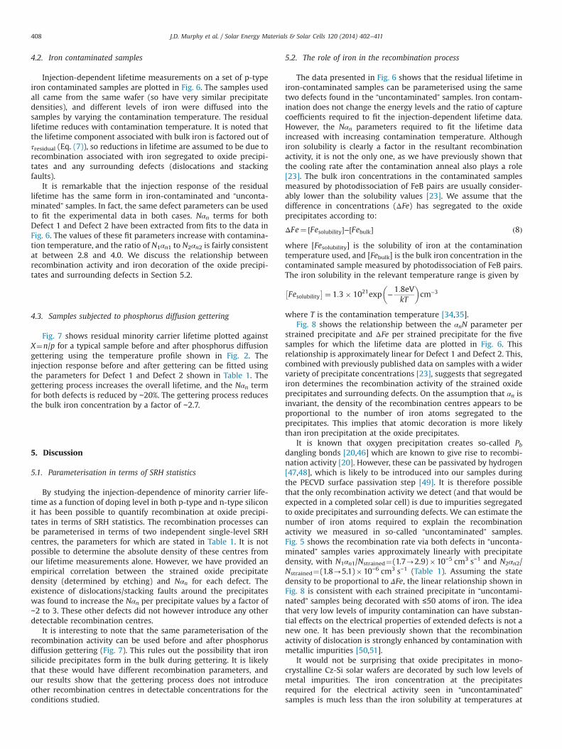
Fig. 9. Simulated product of state density and residual minority carrier lifetimeversus excess minority carrier density in p-type and n-type silicon. The simulationuses the values of ET and Q in Table 1, and assumes αn1¼2�10−6 cm3 s−1 andαn2¼4�10−7 cm3 s−1. Temperature is taken as 25 1C.
J.D. Murphy et al. / Solar Energy Materials & Solar Cells 120 (2014) 402–411 409
used in solar cell processing. Haunschild et al. found a 10 s thermaltreatment at 800 1C to result in a strong enhancement of therecombination activity of rings of oxide precipitates. Their thermalprocess would have been sufficient to redistribute low concentra-tions of bulk iron in the material, resulting in increased irondecoration of the precipitates. The efficiency reductions of up to 4%(absolute) that can arise due to oxygen precipitation in Cz-Si [7], istherefore likely to involve transition metal contamination of theprecipitates and surrounding defects.
It is interesting to note that the recombination activity of oxideprecipitates in both “uncontaminated” and contaminated samplesappears to be approximately dependent upon precipitate densityand not size. An explanation for this is that iron segregates toregions of the precipitates whose number is invariant with size,such as in the vicinity of precipitate corners.
5.3. Extended versus point-like defects
It is interesting that although oxide precipitates and surround-ing dislocations and stacking faults are extended defects, we findthat their effect on bulk minority carrier lifetime is that expectedfrom point-like defects. Our measurements were obtained in awide range of samples (both types, different doping levels, a widerange of precipitate densities of morphologies, with/without ironcontamination) and previously at different temperatures [21].Using our lifetime study alone, we have yet to find any feature ofthe process which cannot be explained using SRH statistics. Wenote that others have applied a SRH-like approach to this problemin the past [52,53]. However, we also acknowledge that otherprevious studies have invoked forms of barrier-controlled captureat the precipitates [54]. Reconciliation of the two approaches is atopic that requires further study.
5.4. Lifetime in n-type and p-type silicon
There has been considerable recent interest in producing photo-voltaics from n-type silicon substrates [55]. This is at partly becausen-type material can have very high carrier lifetimes [56] due to theabsence of light-induced degradation in boron-free material [57], andreduced recombination at interstitial iron [30,45]. Do oxide precipi-tates and associated defects affect recombination in one type morethan another? The parameterisation established here and previously[21,23] can be used to estimate this.
We have established that iron decoration of oxide precipitatesstrongly enhances the recombination activity, so for a fair compar-ison we need to account for the iron decoration. Fitting the injection-dependent lifetime data alone does not allow for the separation ofthe state density (N) from the capture coefficient for electrons orholes (αn or αp, respectively). However, from assuming all therecombination activity arises due to iron decoration, we havepreviously combined iron-loss measurements with the lifetime datato estimate αn1¼2�10−6 cm3 s−1 and αn2¼4�10−7 cm3 s−1 [23]. Thisassumes that each iron atom at an oxide precipitate gives rise to oneof each of Defect 1 and Defect 2. We can use the values of Q in Table 1to estimate αp1¼1.3�10−8 cm3 s−1 and αp2¼4.8�10−4 cm3 s−1.Under the stated assumptions, this gives us the full parameterisationnecessary to estimate carrier lifetime due to iron-decorated oxideprecipitates in p-type and n-type silicon.
A plot of minority carrier lifetime multiplied by state density(N¼N1¼N2) versus excess minority carrier concentration in n-type and p-type silicon with different doping levels is shown inFig. 9. Under the assumptions stated above, the state density is thedensity of iron atoms at the oxide precipitates. The estimatedresidual minority carrier lifetime depends strongly upon dopinglevel and injection level, with the lifetimes at high injectiontending to the ambipolar lifetime. At typical substrate doping
levels for photovoltaics (∼1016 cm−3), the lifetime in p-type mate-rial is higher than in n-type for injection levels at which thelifetime is not at the ambipolar limit. For higher substrate dopinglevels the lifetime benefit of p-type over n-type becomes moresubstantial. For lower substrate doping levels, the lifetime valuesare similar in the p-type and n-type cases, with any predicteddifferences likely to lie within the errors of the SRH parameters. Insummary, the recombination activity associated with just the(iron-decorated) oxide precipitates is slightly better in typicalp-type PV substrates than in n-type. That said, the increasedrecombination activity at bulk interstitial iron in p-type material[30,45] could easily eliminate any possible advantage.
5.5. Competition between gettering systems
In silicon wafers for integrated circuits oxide precipitates andassociated defects are frequently used as a way of internallygettering transition metal impurities, thus preventing the impu-rities harming the devices [5,6]. We performed phosphorus diffu-sion gettering on samples containing oxide precipitates, whichenables us to assess the relative strength of the two getteringsystems. For the results shown in Fig. 7, the bulk iron concentra-tion was 1.4�1012 cm−3 before gettering and 5.2�1011 cm−3 aftergettering, and Nαn terms associated with the oxide precipitates fellby ∼20%. As we have shown that the Nαn parameters correlate withthe iron lost to the precipitates (Fig. 8), we conclude that the bulkiron lost has not been gettered to the oxide precipitates, and hasmost likely been gettered to the phosphorus diffused layer. Thus,for the conditions investigated, phosphorus diffusion gettering ismore effective at gettering bulk iron than oxide precipitates. Thisis very encouraging from the perspective of solar wafers contain-ing oxide precipitates and suggests that the recombination activ-ities will not increase (and may decrease slightly) during thephosphorus diffusion gettering process. It is also noted that ourfindings are consistent with those of Rinio et al., who foundevidence to suggest that impurities are gettered preferentially tothe emitter rather than native crystal defects in mc-Si [58].
The correlation between iron loss and recombination activityshown in Fig. 8 implies that our analysis approach is capable ofmeasuring very low relative concentrations of atomic iron at oxideprecipitates. The results presented in Fig. 7 show that the statesassociated with oxide precipitates are reduced by ∼20% by the

J.D. Murphy et al. / Solar Energy Materials & Solar Cells 120 (2014) 402–411410
phosphorus diffusion gettering process used. An explanation forthis reduction is that this proportion of iron has dissociated fromthe oxide precipitates and surrounding defects. The future focus ofour research is to use this approach with different thermalconditions to understand the fundamental thermodynamics ofthe interaction between iron and oxide precipitates.
6. Conclusions
As a consequence of using fast crystal pulling rates, somemonocrystalline Cz-Si solar wafers contain vacancy-rich regionswhich act as preferential sites for precipitation of supersaturatedbulk oxygen. Oxide precipitates and surrounding defects areassociated with recombination activity, and this can have asubstantial detrimental impact on the conversion efficiency ofsolar cells. We have used injection-dependent minority carrierlifetime measurements to study this recombination activity in∼100 samples with different types, doping levels, precipitatemorphologies and sizes. In all cases we find the lifetime can beparameterised in terms of two independent defect states. The firstdefect is at EV+0.22 eV and has a capture coefficient for electrons∼157 times greater than that for holes. The second defect is atEC−0.08 eV and has a capture coefficient for holes �1200 timesgreater than that for electrons. The concentration of centresappears to scale with the density (not size) of the precipitates,with surrounding dislocations and stacking faults increasing thedensity of centres per precipitate.
Remarkably, we find the same defect states in oxideprecipitate-containing samples which have been intentionallycontaminated with iron. The density of the states per precipitateis dependent on the iron loss from the bulk per precipitate. Wetherefore conclude that at least some of the recombination activityof oxide precipitates in “uncontaminated” samples is due to thesegregation of iron to the precipitates and surrounding defects. Wefind that a phosphorus diffusion gettering process reduces thedensity of states associated with the oxide precipitates by ∼20%,and that bulk iron is preferentially gettered to the phosphorusdiffused layer rather than to the oxide precipitates.
Acknowledgements
The authors thank D. Gambaro, M. Cornara, and M. Olmo(SunEdison) for performing precipitation treatments and charac-terization, R. Chakalova (University of Oxford) for assistance withsample cleaning and surface passivation, and P.R. Wilshaw (Uni-versity of Oxford) for helpful discussions. JDM is the holder of aRoyal Academy of Engineering/EPSRC Research Fellowship and anEPSRC First Grant (EP/J01768X/1).
References
[1] A. Borghesi, B. Pivac, A. Sassella, A. Stella, Oxygen precipitation in silicon,Journal of Applied Physics 77 (1995) 4169.
[2] W. Bergholz, M.J. Binns, G.R. Booker, J.C. Hutchison, S.H. Kinder, S. Messoloras,R.C. Newman, R.J. Stewart, J.G. Wilkes, A study of oxygen precipitation insilicon using high-resolution transmission electron microscopy, small-angleneutron scattering and infrared absorption, Philosophical Magazine B 59(1989) 499.
[3] R. Falster, V.V. Voronkov, V.Y. Resnik, M.G. Milvidskii, Thresholds for effectiveinternal gettering in silicon wafers, Proceedings of the Electrochemical Society,High Purity Silicon, VIII, 2004, pp. 188–201.
[4] R.C. Newman, Oxygen diffusion and precipitation in Czochralski silicon,Journal of Physics: Condensed Matter 12 (2000) R335.
[5] S.M. Myers, M. Seibt, W. Schröter, Mechanisms of transition-metal gettering insilicon, Journal of Applied Physics 88 (2000) 3795.
[6] R.J. Falster, W. Bergholz, The gettering of transition metals by oxygen-relateddefects in silicon, Journal of the Electrochemical Society 137 (1990) 1548.
[7] J. Haunschild, I.E. Reis, J. Geilker, S. Rein, Detecting efficiency-limitingdefects in Czochralski-grown silicon wafers in solar cell production usingphotoluminescence imaging, Physica Status Solidi Rapid Research Letters 5(2011) 199.
[8] P.K. Kulshreshtha, Y. Yoon, K.M. Youssef, E.A. Good, G. Rozgonyi, Oxygenprecipitation related stress-modified crack propagation in high growth rateCzochralski silicon wafers, Journal of the Electrochemical Society 159 (2012)H125.
[9] R. Søndena, Y. Hu, M. Juel, M.S. Wiig, H. Angelskår, Characterization of the OSF-band structure in n-type Cz-Si using photoluminescence-imaging and visualinspection, Journal of Crystal Growth 367 (2013) 68.
[10] K. Youssef, M. Shi, C. Radue, E. Good, G. Rozgonyi, Effect of oxygen andassociated residual stresses on the mechanical properties of high growth rateCzochralski silicon, Journal of Applied Physics 113 (2013) 133502.
[11] H.J. Möller, C. Funke, A. Lawerenz, S. Riedel, M. Werner, Oxygen and latticedistortions in multicrystalline silicon, Solar Energy Materials & Solar Cells 72(2002) 403.
[12] K. Bothe, K. Ramspeck, D. Hinken, C. Schinke, J. Schmidt, S. Herlufsen,R. Brendel, J. Bauer, J.-M. Wagner, N. Zakharov, O. Breitenstein, Luminescenceemission from forward- and reverse-biased multicrystalline silicon solar cells,Journal of Applied Physics 106 (2009) 104510.
[13] M. Tajima, Y. Iwata, F. Okayama, H. Toyota, H. Onodera, T. Sekiguchi, Deep-levelphotoluminescence due to dislocations and oxygen precipitates in multi-crystalline Si, Journal of Applied Physics 111 (2012) 113523.
[14] V.V. Voronkov, R. Falster, Grown-in microdefects, residual vacancies andoxygen precipitation bands in Czochralski silicon, Journal of Crystal Growth204 (1999) 462.
[15] V.V. Voronkov, The mechanism of swirl defects formation in silicon, Journal ofCrystal Growth 59 (1982) 625.
[16] L. Chen, X. Yu, P. Chen, P. Wang, X. Gu, J. Lu, D. Yang, Effect of oxygenprecipitation on the performance of Czochralski silicon solar cells, SolarEnergy Materials & Solar Cells 95 (2011) 3148.
[17] W. Seifert, M. Kittler, M. Seibt, A. Buczkowski, Contrastive recombinationbehaviour of metal silicide and oxygen precipitates in n-type silicon: attemptat an explanation, Solid State Phenomena 47–48 (1996) 365–370.
[18] F.G. Kirscht, Y. Furukawa, W. Seifert, K. Schmalz, A. Buczkowski, S.B. Kim,H. Abe, H. Koya, J. Bailey, Electrical characteristics of oxygen precipitationrelated defects in Czochralski silicon wafers, Materials Science and Engineer-ing B 36 (1996) 230–236.
[19] J.D. Murphy, K. Bothe, M. Olmo, V.V. Voronkov, R.J. Falster, The effect of oxideprecipitates on minority carrier lifetime in p-type silicon, Journal of AppliedPhysics 110 (2011) 053713.
[20] V. Lang, J.D. Murphy, R.J. Falster, J.J.L. Morton, Spin-dependent recombinationin Czochralski silicon containing oxide precipitates, Journal of Applied Physics111 (2012) 013710.
[21] J.D. Murphy, K. Bothe, R. Krain, V.V. Voronkov, R.J. Falster, Parameterisation ofinjection-dependent lifetime measurements in semiconductors in terms ofShockley–Read–Hall statistics: an application to oxide precipitates in silicon,Journal of Applied Physics 111 (2012) 113709.
[22] K. Bothe, R.J. Falster, J.D. Murphy, Room temperature sub-bandgap photo-luminescence from silicon containing oxide precipitates, Applied PhysicsLetters 101 (2012) 032107.
[23] J.D. Murphy, K. Bothe, V.V. Voronkov, R.J. Falster, On the mechanism ofrecombination at oxide precipitates in silicon, Applied Physics Letters 102(2013) 042105.
[24] W. Shockley, W.T. Read, Statistics of the recombinations of holes and electrons,Physical Review 87 (1952) 835.
[25] R.N. Hall, Electron–hole recombination in germanium, Physical Review 87(1952) 387.
[26] D. Macdonald, A. Cuevas, Validity of simplified Shockley–Read–Hall statisticsfor modeling carrier lifetimes in crystalline silicon, Physical Review B:Condensed Matter 67 (2003) 075203.
[27] S. Rein, T. Rehrl, W. Warta, S.W. Glunz, Lifetime spectroscopy for defectcharacterization: systematic analysis of the possibilities and restrictions,Journal of Applied Physics 91 (2002) 2059.
[28] D. Macdonald, A. Cuevas, Trapping of minority carriers in multicrystallinesilicon, Applied Physics Letters 74 (1999) 1710.
[29] A.G. Aberle, T. Lauinger, J. Schmidt, R. Hezel, Injection-level dependent surfacerecombination velocities at the silicon-plasma silicon nitride interface,Applied Physics Letters 66 (1995) 2828.
[30] S. Rein, S.W. Glunz, Electronic properties of interstitial iron and iron–boronpairs determined by means of advanced lifetime spectroscopy, Journal ofApplied Physics 98 (2005) 113711.
[31] J. Schmidt, Effect of dissociation of iron–boron pairs in crystalline silicon onsolar cell properties, Progress in Photovoltaics: Research and Applications 13(2005) 325.
[32] H. Nagel, B. Lenkeit, W. Schmidt, Fill factor losses due to injection-leveldependent bulk lifetimes in crystalline silicon solar cells, in: 20th EuropeanPhotovoltaic Solar Energy Conference, Barcelona, Spain, 2005, pp. 1271–1274.
[33] M.A. Green, Intrinsic concentration, effective densities of states, and effectivemass in silicon, Journal of Applied Physics 67 (1990) 2944.
[34] J.D. Murphy, R.J. Falster, Contamination of silicon by iron at temperaturesbelow 800 1C, Physica Status Solidi Rapid Research Letters 5 (2011) 370.
[35] J.D. Murphy, R.J. Falster, The relaxation behaviour of supersaturated iron insingle-crystal silicon at 500–750 1C, Journal of Applied Physics 112 (2012)113506.
J.D. Murphy et al. / Solar Energy Materials & Solar Cells 120 (2014) 402–411 411
[36] T. Lauinger, J. Moschner, A.G. Aberle, R. Hezel, Optimization and characteriza-tion of remote plasma-enhanced chemical vapor deposition silicon nitride forthe passivation of p-type crystalline silicon surfaces, Journal of VacuumScience & Technology A 16 (1998) 530.
[37] P. Karzel, P. Frey, S. Fritz, G. Hahn, Influence of hydrogen on interstitial ironconcentration in multicrystalline silicon during annealing steps, Journal ofApplied Physics 113 (2013) 114903.
[38] R.A. Sinton, A. Cuevas, Contactless determination of current–voltage charac-teristics and minority-carrier lifetimes in semiconductors from quasi-steady-state photoconductance data, Applied Physics Letters 69 (1996) 2510.
[39] K. Bothe, J. Schmidt, Electronically activated boron–oxygen-related recombi-nation centers in crystalline silicon, Journal of Applied Physics 99 (2006)013701.
[40] G. Zoth, W. Bergholz, A fast, preparation-free method to detect iron in silicon,Journal of Applied Physics 67 (1990) 6764.
[41] W. Wijaranakula, The reaction kinetics of iron–boron pair formation anddissociation in p-type silicon, Journal of the Electrochemical Society 140(1993) 275.
[42] D.H. Macdonald, L.J. Geerligs, A. Azzizi, Iron detection in crystalline silicon bycarrier lifetime measurements for arbitrary injection and doping, Journal ofApplied Physics 95 (2004) 1021.
[43] H. Schlangenotto, H. Maeder, W. Gerlach, Temperature dependence of theradiative recombination coefficient in silicon, Physica Status Solidi A Applica-tions and Material Science 21 (1974) 357.
[44] M.J. Kerr, A. Cuevas, General parameterization of Auger recombination incrystalline silicon, Journal of Applied Physics 91 (2002) 2473.
[45] D. Macdonald, L.J. Geerligs, Recombination activity of interstitial iron andother transition metal point defects in p- and n-type crystalline silicon,Applied Physics Letters 85 (2004) 4061.
[46] M. Koizuka, H. Yamada-Kaneta, Electron spin resonance centers associatedwith oxygen precipitates in Czochralski silicon crystals, Journal of AppliedPhysics 88 (2000) 1784.
[47] M. Koizuka, H. Yamada-Kaneta, Gap states caused by oxygen precipitation inCzochralski silicon crystals, Journal of Applied Physics 84 (1998) 4255.
[48] E. Cartier, J.H. Stathis, D.A. Buchanan, Passivation and depassivation of silicondangling bonds at the Si/SiO2 interface by atomic hydrogen, Applied PhysicsLetters 63 (1993) 1510.
[49] A.G. Aberle, Overview on SiN surface passivation of crystalline silicon solarcells, Solar Energy Materials and Solar Cells 65 (2001) 239–248.
[50] V. Kveder, M. Kittler, W. Schröter, Recombination activity of contaminateddislocations in silicon: a model describing electron-beam-induced currentcontrast behavior, Physical Review B: Condensed Matter 63 (2001) 115208.
[51] T.S. Fell, P.R. Wilshaw, M.D. de Coteau, EBIC investigations of dislocations andtheir interactions with impurities in silicon, Physica Status Solidi A Applica-tions and Material Science 138 (1993) 695.
[52] J. Vanhellemont, E. Simoen, A. Kaniava, M. Libezny, C. Claeys, Impact of oxygenrelated extended defects on silicon diode characteristics, Journal of AppliedPhysics 77 (1995) 5669.
[53] W. Seifert, M. Kittler, J. Vanhellemont, EBIC study of recombination activity ofoxygen precipitation related defects in Si, Materials Science and Engineering B42 (1996) 260.
[54] J.M. Hwang, D.K. Schroder, Recombination properties of oxygen-precipitatedsilicon, Journal of Applied Physics 59 (1986) 2476.
[55] D. Macdonald, The emergence of n-type silicon for solar cell manufacture, in:50th Annual AuSES Conference (Solar 2012), Melbourne, Australia, 2012.
[56] A. Cuevas, M.J. Kerr, C. Samundsett, F. Ferrazza, G. Coletti, Millisecond minoritycarrier lifetimes in n-type multicrystalline silicon, Applied Physics Letters 81(2002) 4952.
[57] T. Schutz-Kuchly, J. Veirman, S. Dubois, D.R. Heslinga, Light-Induced-Degradation effects in boron–phosphorus compensated n-type Czochralskisilicon, Applied Physics Letters 96 (2010) 093505.
[58] M. Rinio, A. Yodyunyong, S. Keipert-Colberg, Y.P.B. Mouafi, D. Borchert,A. Montesdeoca-Santana, Improvement of multicrystalline silicon solar cellsby a low temperature anneal after emitter diffusion, Progress in Photovoltaics:Research and Applications 19 (2011) 165.