microelectronics elct 703 (w19) op-amp …eee.guc.edu.eg/courses/electronics/elct703...example find...
TRANSCRIPT
MICROELECTRONICS ELCT 703 (W19)LECTURE 6 : OP-AMP LINEAR/NONLINEAR
APPLICATIONS
Dr. Eman Azab
Assistant Professor
Office: C3.315
E-mail:
[email protected]. EMAN AZAB
ELECTRONICS DEPT., FACULTY OF IET
THE GERMAN UNIVERSITY IN CAIRO
1
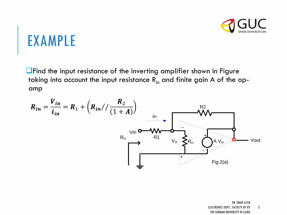
EXAMPLE
Find the input resistance of the inverting amplifier shown in Figure taking into account the input resistance Rin and finite gain A of the op-amp
DR. EMAN AZAB
ELECTRONICS DEPT., FACULTY OF IET
THE GERMAN UNIVERSITY IN CAIRO
2
R2
R1Vin
Vout
_
+
RinVid
+
-
A Vid
Rin
Fig.2(a)
iin
𝑹𝒊𝒏 =𝑽𝒊𝒏
𝒊𝒊𝒏= 𝑹1 + 𝑹𝒊𝒏 /
𝑹2
1 + 𝑨

NON-IDEALITIES EFFECT ON OP-AMP APPLICATIONS Linear and Non-linear
Applications
DR. EMAN AZAB
ELECTRONICS DEPT., FACULTY OF IET
THE GERMAN UNIVERSITY IN CAIRO
3

VOLTAGE AMPLIFIER
DR. EMAN AZAB
ELECTRONICS DEPT., FACULTY OF IET
THE GERMAN UNIVERSITY IN CAIRO
4
Inverting and Non-Inverting Amplifiers
𝑣𝑂𝑣𝐼
= −𝑅2𝑅1
𝑣𝑂𝑣𝐼
= 1 +𝑅2𝑅1
Figure from Sedra/Smith Copyright © 2010 by Oxford University Press, Inc.
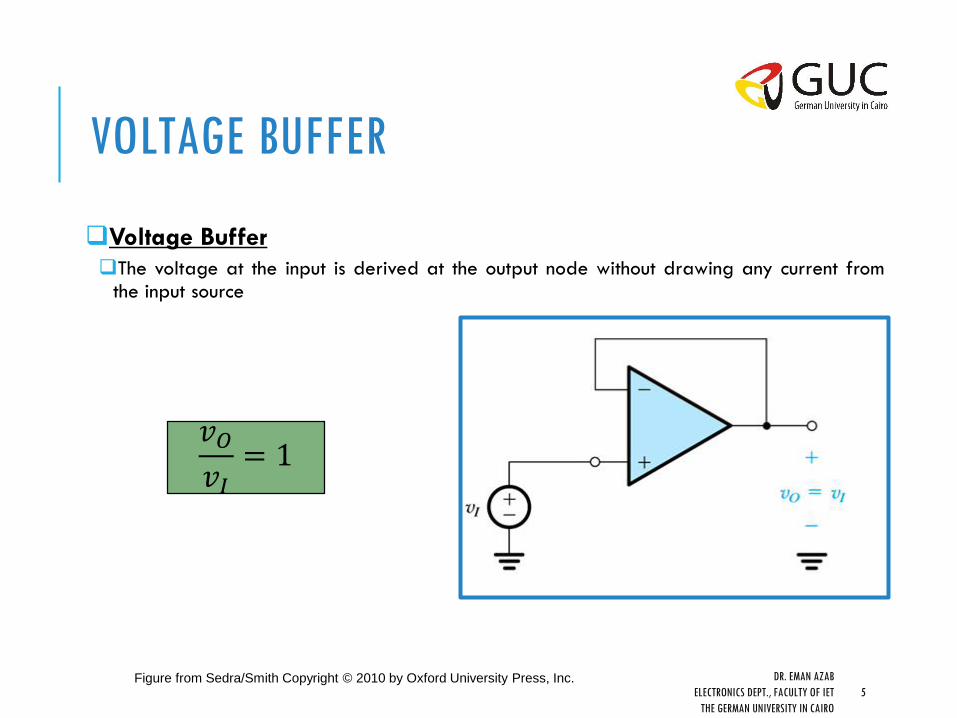
VOLTAGE BUFFER
DR. EMAN AZAB
ELECTRONICS DEPT., FACULTY OF IET
THE GERMAN UNIVERSITY IN CAIRO
5
Voltage Buffer
The voltage at the input is derived at the output node without drawing any current fromthe input source
𝑣𝑂𝑣𝐼
= 1
Figure from Sedra/Smith Copyright © 2010 by Oxford University Press, Inc.

VOLTAGE DIFFERENCE AMPLIFIER
DR. EMAN AZAB
ELECTRONICS DEPT., FACULTY OF IET
THE GERMAN UNIVERSITY IN CAIRO
6
The circuit subtracts two voltage signals
By Applying Superposition principle between 𝑣𝐼1 and 𝑣𝐼2
By Choosing:
𝑣𝑂 = −𝑣𝐼1𝑅2𝑅1
+ 𝑣𝐼2𝑅4
𝑅4 + 𝑅31 +
𝑅2𝑅1
Figure from Sedra/Smith Copyright © 2010 by Oxford University Press, Inc.
𝑅2𝑅1
=𝑅4𝑅3
𝑣𝑂 =𝑅2𝑅1
𝑣𝐼2 − 𝑣𝐼1
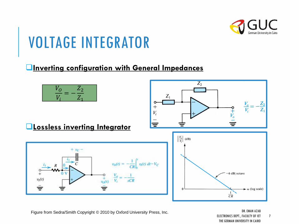
VOLTAGE INTEGRATOR
DR. EMAN AZAB
ELECTRONICS DEPT., FACULTY OF IET
THE GERMAN UNIVERSITY IN CAIRO
7
Inverting configuration with General Impedances
Lossless inverting Integrator
Figure from Sedra/Smith Copyright © 2010 by Oxford University Press, Inc.
𝑉𝑂𝑉𝑖
= −𝑍2𝑍1
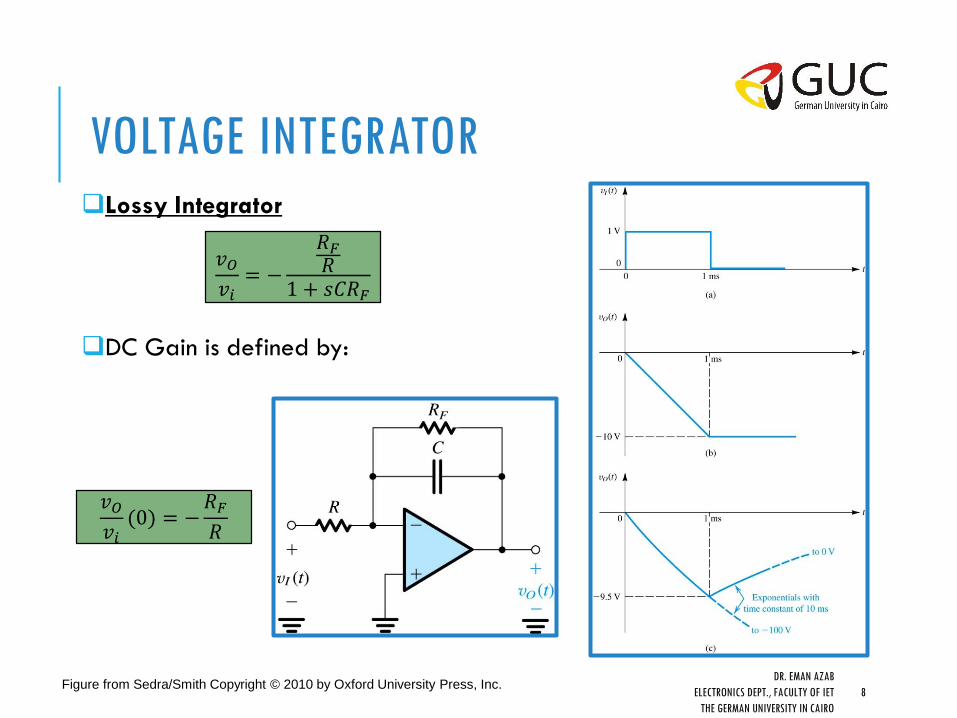
VOLTAGE INTEGRATOR
DR. EMAN AZAB
ELECTRONICS DEPT., FACULTY OF IET
THE GERMAN UNIVERSITY IN CAIRO
8
Lossy Integrator
DC Gain is defined by:
Figure from Sedra/Smith Copyright © 2010 by Oxford University Press, Inc.
𝑣𝑂𝑣𝑖
= −
𝑅𝐹𝑅
1 + 𝑠𝐶𝑅𝐹
𝑣𝑂𝑣𝑖
(0) = −𝑅𝐹𝑅
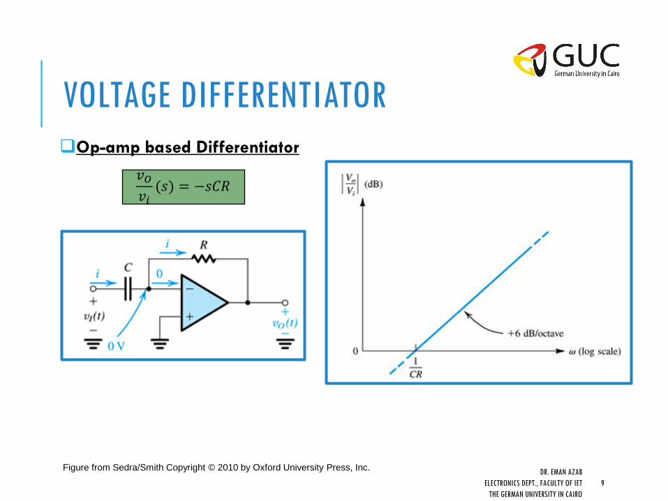
VOLTAGE DIFFERENTIATOR
DR. EMAN AZAB
ELECTRONICS DEPT., FACULTY OF IET
THE GERMAN UNIVERSITY IN CAIRO
9
Op-amp based Differentiator
Figure from Sedra/Smith Copyright © 2010 by Oxford University Press, Inc.
𝑣𝑂𝑣𝑖
(𝑠) = −𝑠𝐶𝑅
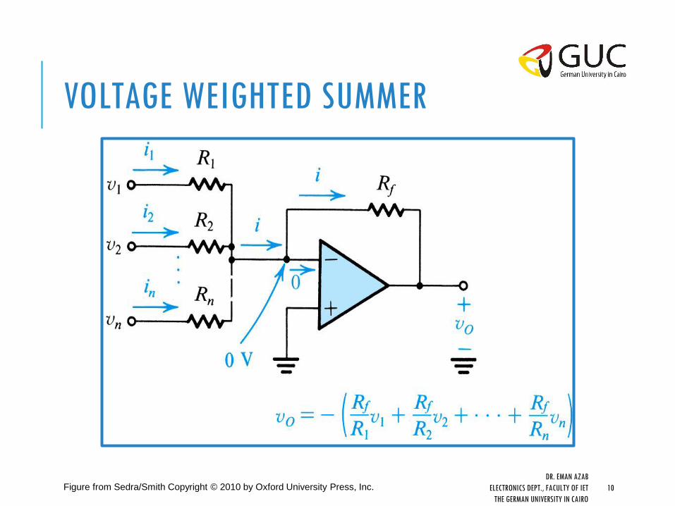
VOLTAGE WEIGHTED SUMMER
DR. EMAN AZAB
ELECTRONICS DEPT., FACULTY OF IET
THE GERMAN UNIVERSITY IN CAIRO
10Figure from Sedra/Smith Copyright © 2010 by Oxford University Press, Inc.
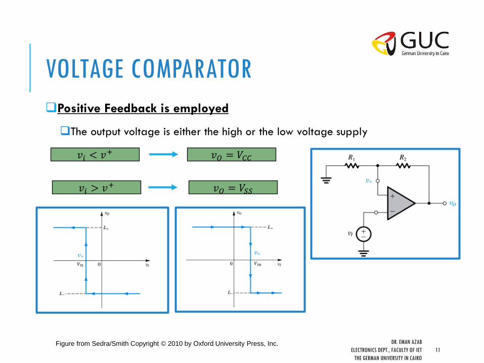
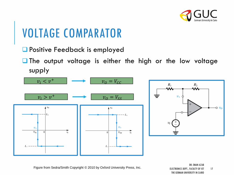
VOLTAGE COMPARATOR
DR. EMAN AZAB
ELECTRONICS DEPT., FACULTY OF IET
THE GERMAN UNIVERSITY IN CAIRO
11Figure from Sedra/Smith Copyright © 2010 by Oxford University Press, Inc.
Positive Feedback is employed
The output voltage is either the high or the low voltage supply
𝑣𝑖 < 𝑣+ 𝑣𝑂 = 𝑉𝐶𝐶
𝑣𝑖 > 𝑣+ 𝑣𝑂 = 𝑉𝑆𝑆

VOLTAGE LOGARITHMIC AMPLIFIER
DR. EMAN AZAB
ELECTRONICS DEPT., FACULTY OF IET
THE GERMAN UNIVERSITY IN CAIRO
12
Non-linear logarithmic Amplifier
BJT operates in the Active Region
𝑉𝑜𝑢𝑡 = −𝑉𝐵𝐸 = −𝑉𝑇𝑙𝑛𝐼𝐶𝐼𝑜
𝐼𝐶 =𝑉𝑖𝑛𝑅1
𝑉𝑜𝑢𝑡 = −𝑉𝐵𝐸 = −𝑉𝑇𝑙𝑛𝑉𝑖𝑛𝐼𝑜𝑅1
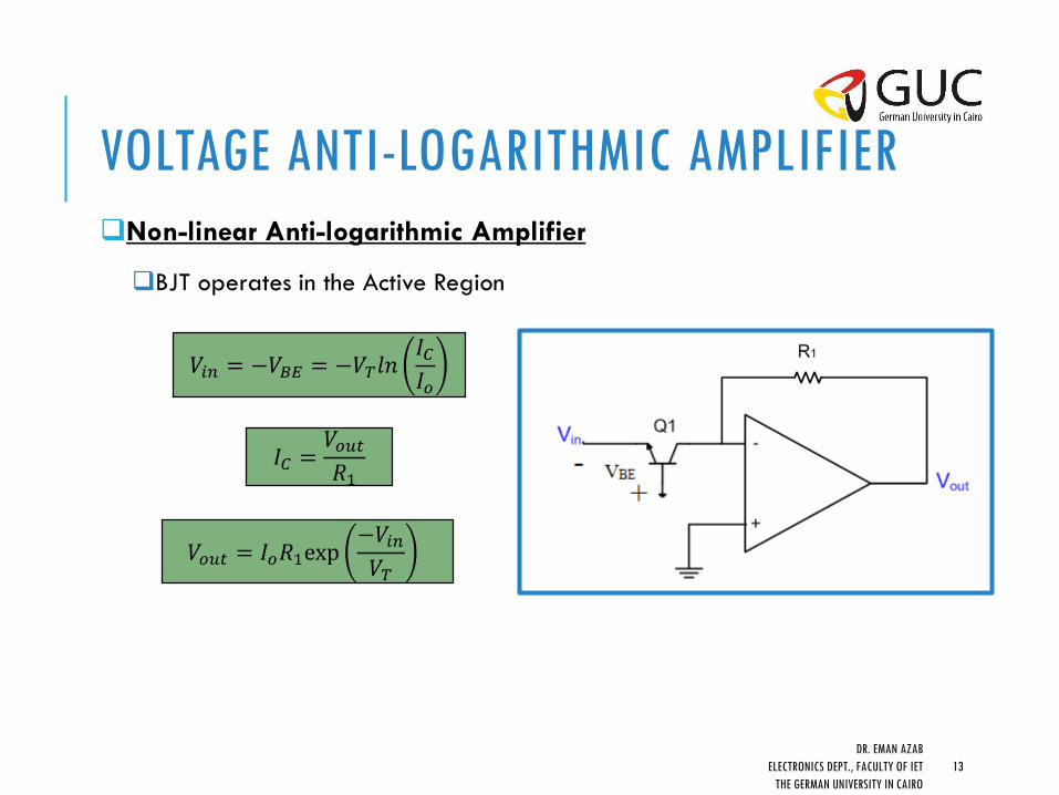
VOLTAGE ANTI-LOGARITHMIC AMPLIFIER
DR. EMAN AZAB
ELECTRONICS DEPT., FACULTY OF IET
THE GERMAN UNIVERSITY IN CAIRO
13
Non-linear Anti-logarithmic Amplifier
BJT operates in the Active Region
𝑉𝑖𝑛 = −𝑉𝐵𝐸 = −𝑉𝑇𝑙𝑛𝐼𝐶𝐼𝑜
𝐼𝐶 =𝑉𝑜𝑢𝑡𝑅1
𝑉𝑜𝑢𝑡 = 𝐼𝑜𝑅1exp−𝑉𝑖𝑛𝑉𝑇

EXAMPLE
DR. EMAN AZAB
ELECTRONICS DEPT., FACULTY OF IET
THE GERMAN UNIVERSITY IN CAIRO
14
For the 4127 IC showed in figure, find the output voltage (Vout) as a function in the input currents (Ix and Iy).
Using the 4127 IC and the linear/nonlinear op-amp applications, design the following functions with minimum number of op-amps and derive K, n and m as a function in the circuit parameters.
Note that: Q1 and Q2 are matched and β is large.
𝑉𝑜𝑢𝑡 = 𝐾𝐼𝑥𝐼𝑦
𝑚
𝑉𝑜𝑢𝑡 = 𝐾𝐼𝑥𝐼𝑦
𝑚−𝑛
WAVE-FUNCTION GENERATORS
Introduction
DR. EMAN AZAB
ELECTRONICS DEPT., FACULTY OF IET
THE GERMAN UNIVERSITY IN CAIRO
15
INTRODUCTION
DR. EMAN AZAB
ELECTRONICS DEPT., FACULTY OF IET
THE GERMAN UNIVERSITY IN CAIRO
16
Oscillators (Wave-Function Generators) are used in all
communication systems
They are used to generate sinusoidal or triangular wave
forms with adjustable magnitude and frequency
There is different architectures and designs for these
circuits, we will focus on the designs using voltage op-
amps
Op-amp based Oscillators are critically stable closed-
loop systems designed using positive feedback
Op-amp comparators are the basic building block for the
oscillators
VOLTAGE COMPARATOR
DR. EMAN AZAB
ELECTRONICS DEPT., FACULTY OF IET
THE GERMAN UNIVERSITY IN CAIRO
17Figure from Sedra/Smith Copyright © 2010 by Oxford University Press, Inc.
Positive Feedback is employed
The output voltage is either the high or the low voltage
supply
𝑣𝑖 < 𝑣+ 𝑣𝑂 = 𝑉𝐶𝐶
𝑣𝑖 > 𝑣+ 𝑣𝑂 = 𝑉𝑆𝑆
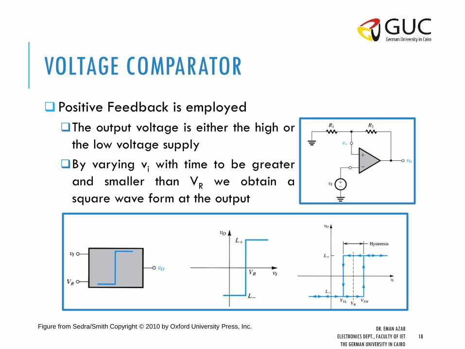
VOLTAGE COMPARATOR
DR. EMAN AZAB
ELECTRONICS DEPT., FACULTY OF IET
THE GERMAN UNIVERSITY IN CAIRO
18
Figure from Sedra/Smith Copyright © 2010 by Oxford University Press, Inc.
Positive Feedback is employed
The output voltage is either the high or
the low voltage supply
By varying vi with time to be greater
and smaller than VR we obtain a
square wave form at the output
SQUARE WAVE-FUNCTION GENERATOR
DR. EMAN AZAB
ELECTRONICS DEPT., FACULTY OF IET
THE GERMAN UNIVERSITY IN CAIRO
19
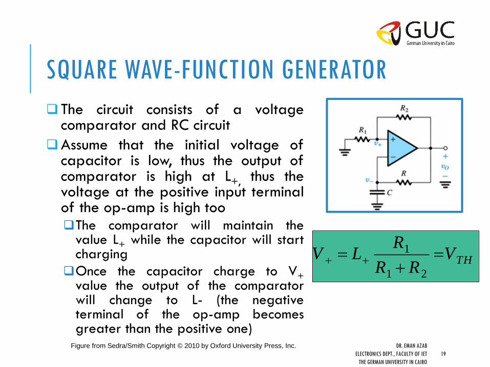
Figure from Sedra/Smith Copyright © 2010 by Oxford University Press, Inc.
The circuit consists of a voltagecomparator and RC circuit
Assume that the initial voltage ofcapacitor is low, thus the output ofcomparator is high at L+, thus thevoltage at the positive input terminalof the op-amp is high tooThe comparator will maintain the
value L+ while the capacitor will startcharging
Once the capacitor charge to V+value the output of the comparatorwill change to L- (the negativeterminal of the op-amp becomesgreater than the positive one)
1
1 2
TH
RV L V
R R
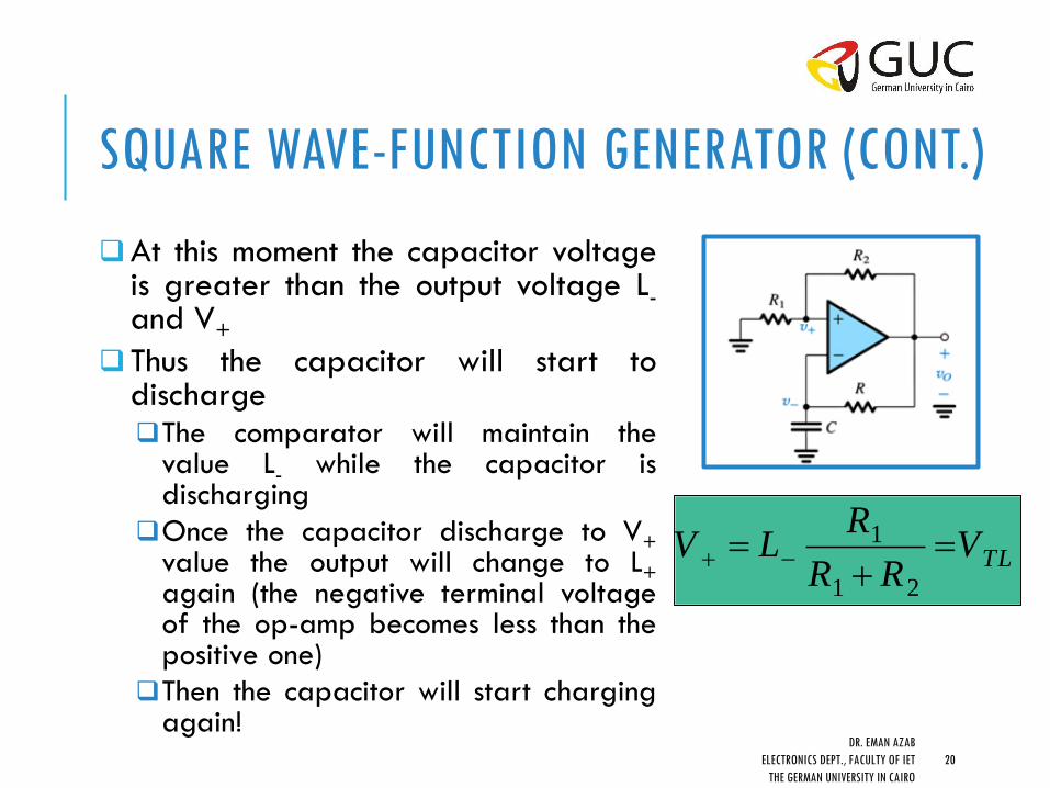
SQUARE WAVE-FUNCTION GENERATOR (CONT.)
DR. EMAN AZAB
ELECTRONICS DEPT., FACULTY OF IET
THE GERMAN UNIVERSITY IN CAIRO
20
At this moment the capacitor voltageis greater than the output voltage L-and V+
Thus the capacitor will start todischargeThe comparator will maintain the
value L- while the capacitor isdischarging
Once the capacitor discharge to V+value the output will change to L+again (the negative terminal voltageof the op-amp becomes less than thepositive one)
Then the capacitor will start chargingagain!
1
1 2
TL
RV L V
R R
SQUARE WAVE-FUNCTION GENERATOR (CONT.)
DR. EMAN AZAB
ELECTRONICS DEPT., FACULTY OF IET
THE GERMAN UNIVERSITY IN CAIRO
21
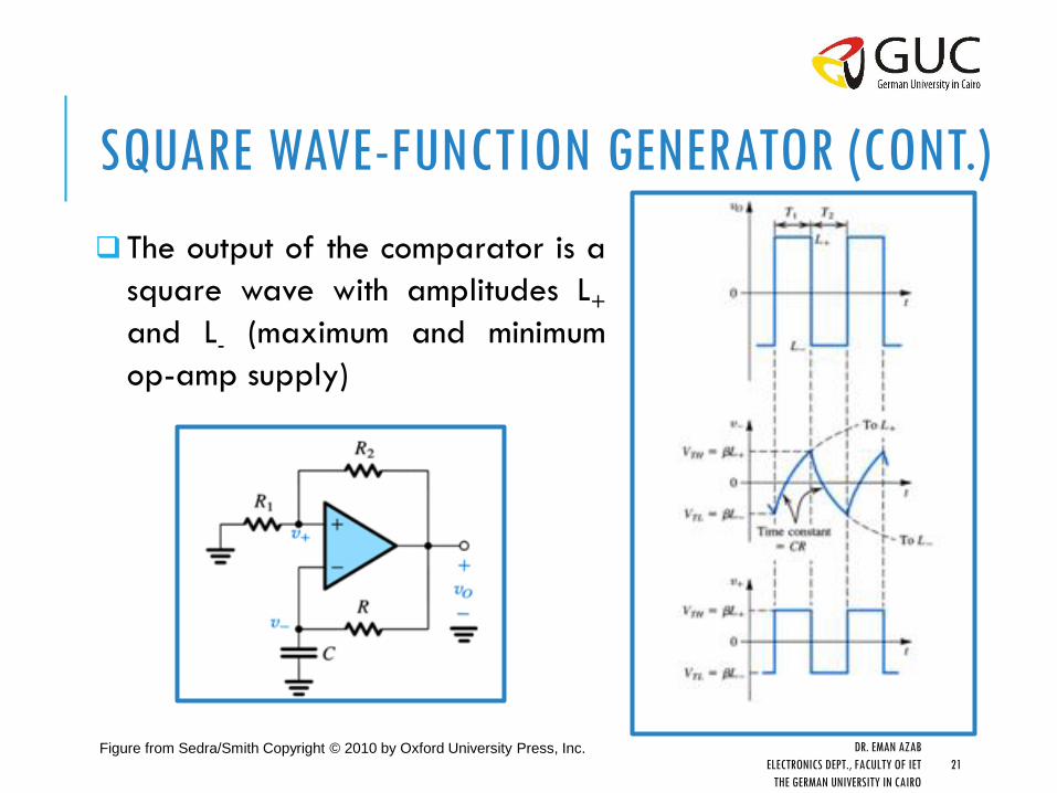
Figure from Sedra/Smith Copyright © 2010 by Oxford University Press, Inc.
The output of the comparator is a
square wave with amplitudes L+
and L- (maximum and minimum
op-amp supply)

SQUARE WAVE-FUNCTION GENERATOR (CONT.)
DR. EMAN AZAB
ELECTRONICS DEPT., FACULTY OF IET
THE GERMAN UNIVERSITY IN CAIRO
22
To calculate the frequency of theoutput wave form, we must calculatethe charging and discharging timeof the capacitor
Where R is the charging resistor, Cis the capacitor used, VSt is thesteady state voltage of thecapacitor (L+ or L-), Vini and VF is theinitial and final capacitor voltagerespectively
𝑇 = 𝑅𝐶 ln𝑉𝑆𝑡 − 𝑉𝑖𝑛𝑖𝑉𝑆𝑡 − 𝑉𝐹
SQUARE WAVE-FUNCTION GENERATOR (CONT.)
DR. EMAN AZAB
ELECTRONICS DEPT., FACULTY OF IET
THE GERMAN UNIVERSITY IN CAIRO
23
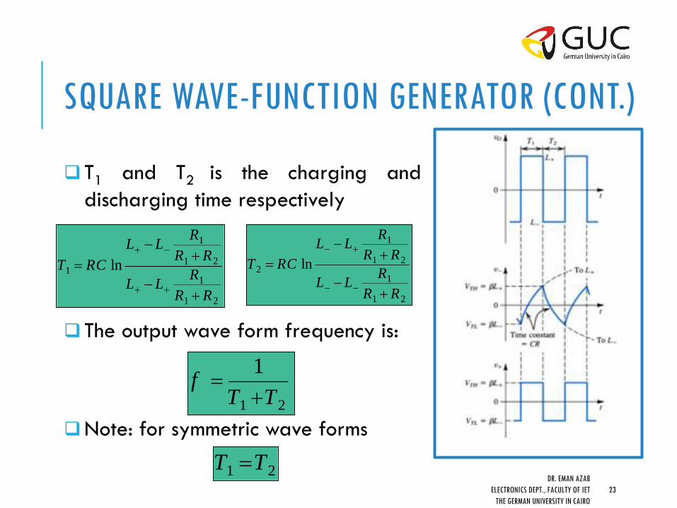
T1 and T2 is the charging and
discharging time respectively
The output wave form frequency is:
Note: for symmetric wave forms
1
1 21
1
1 2
ln
RL L
R RT RC
RL L
R R
1
1 22
1
1 2
ln
RL L
R RT RC
RL L
R R
1 2
1f
T T
1 2T T

TRIANGULAR WAVE-FUNCTION GENERATOR
DR. EMAN AZAB
ELECTRONICS DEPT., FACULTY OF IET
THE GERMAN UNIVERSITY IN CAIRO
24Figure from Sedra/Smith Copyright © 2010 by Oxford University Press, Inc.
A Triangular wave
function generator can be
realized by integrating a
square wave form
Thus adding an op-amp
based integrator after
the square wave function
generator will realize a
triangular waveform
1
1 2
TH
RV L
R R
1
1 2
TL
RV L
R R
TRIANGULAR WAVE FUNCTION GENERATOR (CONT.)
DR. EMAN AZAB
ELECTRONICS DEPT., FACULTY OF IET
THE GERMAN UNIVERSITY IN CAIRO
25
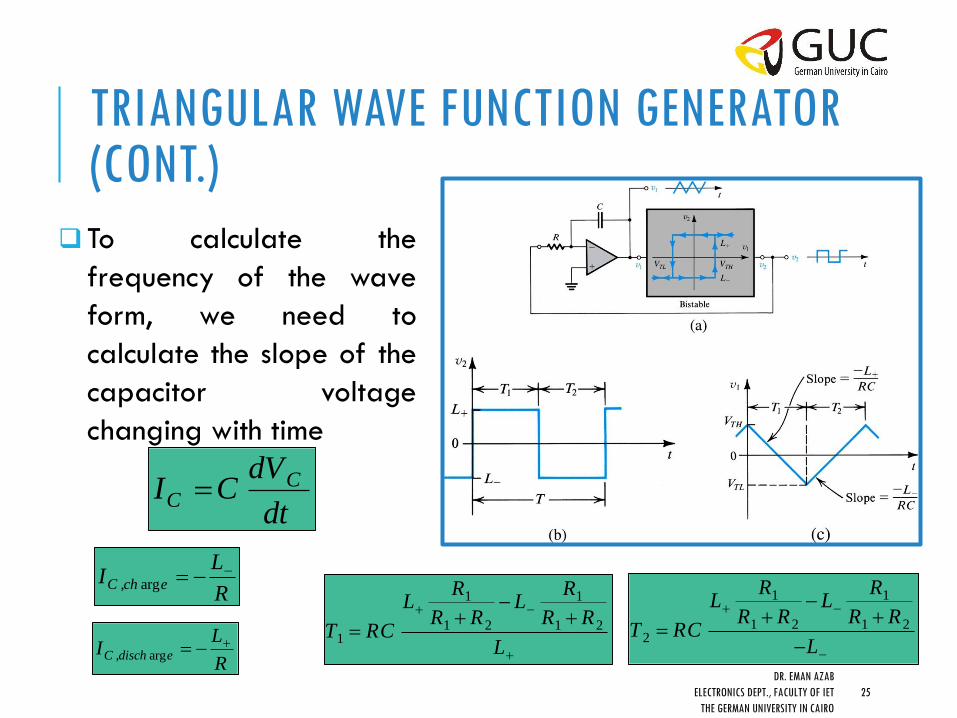
To calculate the
frequency of the wave
form, we need to
calculate the slope of the
capacitor voltage
changing with time
CC
dVI C
dt
, argC ch e
LI
R
, argC disch e
LI
R
1 1
1 2 1 21
R RL L
R R R RT RC
L
1 1
1 2 1 22
R RL L
R R R RT RC
L
EXAMPLE
DR. EMAN AZAB
ELECTRONICS DEPT., FACULTY OF IET
THE GERMAN UNIVERSITY IN CAIRO
26
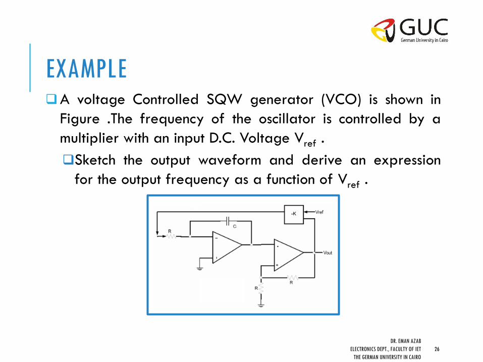
A voltage Controlled SQW generator (VCO) is shown in
Figure .The frequency of the oscillator is controlled by a
multiplier with an input D.C. Voltage Vref .
Sketch the output waveform and derive an expression
for the output frequency as a function of Vref .