ltc1760 dual smart battery system manager - analog.com · integrated smbus level 3 battery charger...
TRANSCRIPT

LTC1760
11760fc
For more information www.linear.com/LTC1760
TYPICAL APPLICATION
FEATURES DESCRIPTION
Dual Smart Battery System Manager
The LTC®1760 Smart Battery System Manager is a highly- integrated SMBus Level 3 battery charger and selector intended for products using dual smart batteries. Three SMBus interfaces allow the LTC1760 to servo to the internal voltage and currents measured by the batteries while allowing an SMBus Host device to monitor either battery’s status. Charging accuracy is determined by the battery’s internal voltage and current measurements, typically better than ±0.2%.
A proprietary PowerPath architecture supports simultane-ous charging or discharging of both batteries. Typical battery run times are extended by up to 10%, while charging times are reduced by up to 50%. The LTC1760 automatically switches between power sources in less than 10µs to prevent power interruption upon battery or wall adapter removal.
The LTC1760 implements all elements of a version 1.1 “Smart Battery System Manager” except for the generation of composite battery information. An internal multiplexer cleanly switches the SMBus Host to either of the two attached Smart Batteries without generating partial mes-sages to batteries or SMBus Host. Thermistors on both batteries are automatically monitored for temperature and disconnection information (SafetySignal).
Dual vs Sequential Charging
APPLICATIONS
n SMBus Charger/Selector for Two Smart Batteries*n Voltage and Current Accuracy within 0.2% of Value
Reported by Batteryn Simplifies Construction of “Smart Battery System
Manager”n Includes All SMBus Charger V1.1 Safety Featuresn Supports Autonomous Operation without a Hostn Allows Both Batteries to Discharge Simultaneously
into Single Load with Low Loss (Ideal Diode) n SMBus Switching for Dual Batteries with Alarm
Monitoring for Charging Battery at All Timesn Pin Programmable Limits for Maximum Charge
Current and Voltage Improve Safetyn Fast Autonomous PowerPath™ Switching (<10µs)n Low Loss Simultaneous Charging of Two Batteriesn >95% Efficient Synchronous Buck Chargern AC Adapter Current Limiting* Maximizes Charge Raten SMBus Accelerator Improves SMBus Timing**n Available in 48-Lead TSSOP Package
n Portable Computers and Instrumentsn Standalone Dual Smart Battery Chargersn Battery Backup Systems
LTC1760
DCIN
SYSTEMPOWER
SMBus (HOST)
1760 TA01
SafetySignal 1
SMBus 1
SafetySignal 2
SMBus 2
TIME (MINUTES)
BATT
ERY
CURR
ENT
(mA)
350030002500200015001000500
0350030002500200015001000500
0
1760 TA03
0 50 100 150 200 250 300
BAT1CURRENT
BAT2CURRENT
SEQUENTIAL
DUAL
BAT1CURRENT
100MINUTES
BATTERY TYPE: 10.8V Li-Ion (MOLTECH NI2020)REQUESTED CURRENT = 3AREQUESTED VOLTAGE = 12.3VMAX CHARGER CURRENT = 4.1A
BAT2CURRENT
Dual Battery Charger/Selector System Architecture
L, LT, LTC, LTM, Linear Technology and the Linear logo are registered trademarks and PowerPath is a trademark of Analog Devices, Inc. All other trademarks are the property of their respective owners. Protected by U.S. Patents including *5723970 **6650174.

LTC1760
21760fc
For more information www.linear.com/LTC1760
PIN CONFIGURATIONABSOLUTE MAXIMUM RATINGS
DCIN, SCP, SCN, CLP, VPLUS, SW to GND ..................................... –0.3V to 32VSCH1, SCH2 to GND ................................... –0.3V to 28VBOOST to GND ........................................... –0.3V to 37VCSP, CSN, BAT1, BAT2 to GND ................... –0.3V to 28VLOPWR, DCDIV to GND ............................. –0.3V to 10VVCC2, VDDS to GND ....................................... –0.3V to 7VSDA1, SDA2, SDA, SCL1, SCL2, SCL, SMBALERT to GND .................... –0.3V to 7VMODE to GND .................................–0.3V to VCC2 +0.3V COMP1 to GND ............................................ –0.3V to 5VMaximum DC Current Into Pin SDA1, SDA2, SDA, SCL1, SCL2, SCL ................ ±3mA TH1A, TH2A ..................................................... –5mA TH1B, TH2B ................................................... –102µAOperating Junction Temperature Range (Note 6) .................................................. –40°C to 125°CStorage Temperature.............................. –65°C to 150°CLead Temperature (Soldering, 10 sec) ................... 300°C
(Note 1)
123456789
101112131415161718192021222324
TOP VIEW
FW PACKAGE48-LEAD PLASTIC TSSOP
484746454443424140393837363534333231302928272625
SCH2GCH2GCH1SCH1TGATEBOOSTSWDCINVCCBGATEPGNDCOMP1CLPCSPCSNVLIMITILIMITTH1BTH1ASMBALERTTH2ATH2BMODEVCC2
VPLUSBAT2BAT1SCNSCP
GDCOGDCIGB1OGB1I
GB2OGB2I
LOPWRVSET
ITHISET
DCDIVSCL2SCL
SCL1VDDSSDA2SDA
SDA1GND
TJMAX = 125°C, qJA = 110°C/W
ORDER INFORMATION
LEAD FREE FINISH TAPE AND REEL PART MARKING PACKAGE DESCRIPTION TEMPERATURE RANGE
LTC1760CFW#PBF LTC1760CFW#TRPBF LTC1760CFW 48-Lead Plastic TSSOP 0°C to 85°C
LTC1760IFW#PBF LTC1760IFW#TRPBF LTC1760IFW 48-Lead Plastic TSSOP –40°C to 125°C
Consult LTC Marketing for parts specified with wider operating temperature ranges. Consult LTC Marketing for information on non-standard lead based finish parts.For more information on lead free part marking, go to: http://www.linear.com/leadfree/ For more information on tape and reel specifications, go to: http://www.linear.com/tapeandreel/. Some packages are available in 500 unit reels through designated sales channels with #TRMPBF suffix.
(http://www.linear.com/product/LTC1760#orderinfo)

LTC1760
31760fc
For more information www.linear.com/LTC1760
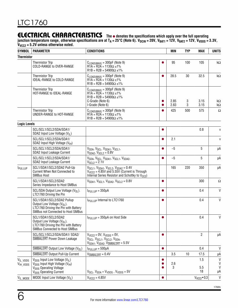
ELECTRICAL CHARACTERISTICS
SYMBOL PARAMETER CONDITIONS MIN TYP MAX UNITS
Supply and Reference
DCIN Operating Range DCIN Selected 6 28 V
ICH0 ICH1
DCIN Operating Current Not Charging (DCIN Selected) (Note 10) Charging (DCIN Selected) (Note 10)
1 1.3
1.5 2
mA mA
IVCC2_AC1 IVCC2_AC0
VCC2 Operating Current AC Present (Note 11) AC Not Present (Note 11)
0.75 75
1 100
mA µA
Battery Operating Voltage Range Battery Selected, PowerPath Function Battery Selected, Charging Function (Note 2)
6 0
28 28
V V
IBAT Battery Drain Current Battery Selected, Not Charging, VDCIN = 0V (Note 10) 175 µA
VFDC VFB1 VFB2 VFSCN
VPLUS Diodes Forward Voltage: DCIN to VPLUS BAT1 to VPLUS BAT2 to VPLUS SCN to VPLUS
IVCC = 10mA IVCC = 0mA IVCC = 0mA IVCC = 0mA
0.8 0.7 0.7 0.7
V V V V
UVLO Undervoltage Lockout Threshold VPLUS Ramping Down, Measured at VPLUS to GND l 3 5 V
VVCC VCC Regulator Output Voltage l 4.9 5.2 5.5 V
VLDR VCC Load Regulation No External Connection Beyond Applications Shown Herein
0.2 1 %
Switching Regulator
VTOL Voltage Accuracy With Respect to Voltage Reported by Battery VCHMIN < Requested Voltage < VLIMIT
l –32 32 mV
ITOL Current Accuracy With Respect to Current Reported by Battery 4mV/RSENSE < Requested Current < ILIMIT (Min) (Note 12) RILIMIT = 0 (Short to GND) RILIMIT = 10k ±1% RILIMIT = 33k ±1% RILIMIT = Open (or Short ILIMIT to VCC2)
l
l
l
l
–2 –4 –8 –8
2 4 8 8
mA mA mA mA
f0SC Regulator Switching Frequency 255 300 345 kHz
fDO Regulator Switching Frequency in Low Dropout Mode
Duty Cycle ≥99% 20 25 kHz
DCMAX Regulator Maximum Duty Cycle 99 99.5 %
IMAX Maximum Current Sense Threshold VITH = 2.2V 140 155 190 mV
ISNS CA1 Input Bias Current VCSP = VCSN > 5V 150 µA
CMSL CA1 Input Common Mode Low 0 V
CMSH CA1 Input Common Mode High VDCIN – 0.2 V
VCL1 CL1 Turn-On Threshold C-Grade (Note 6) I-Grade (Note 6)
l
l
95 94 90
100 100 100
105 108 108
mV mV mV
TG tr TG tr
TGATE Transition Time: TGATE Rise Time TGATE Fall Time
CLOAD = 3300pF, 10% to 90% CLOAD = 3300pF, 10% to 90%
50 50
90 90
ns ns
BG tr BG tf
BGATE Transition Time BGATE Rise Time BGATE Fall Time
CLOAD = 3300pF, 10% to 90% CLOAD = 3300pF, 10% to 90%
50 40
90 80
ns ns
The l denotes the specifications which apply over the full operating junction temperature range, otherwise specifications are at TA = 25°C (Note 6). VDCIN = 20V, VBAT1 = 12V, VBAT2 = 12V, VVDDS = 3.3V, VVCC2 = 5.2V unless otherwise noted.

LTC1760
41760fc
For more information www.linear.com/LTC1760
SYMBOL PARAMETER CONDITIONS MIN TYP MAX UNITS
Trip Points
VTR DCDIV/LOPWR Threshold VDCDIV or VLOPWR Falling C-Grade (Note 6) I-Grade (Note 6)
l
l
1.166 1.162
1.19 1.19
1.215 1.215
V V
VTHYS DCDIV/LOPWR Hysteresis Voltage VDCDIV or VLOPWR Rising 30 mV
IBVT DCDIV/LOPWR Input Bias Current VDCDIV or VLOPWR = 1.19V 20 200 nA
VTSC Short-Circuit Comparator Threshold VSCP – VSCN, VCC ≥ 5V C-Grade (Note 6) I-Grade (Note 6)
l
l
90 88
100 100
115 115
mV mV
VFTO Fast PowerPath Turn-Off Threshold VDCDIV Rising from VCC 6 7 7.9 V
VOVSD Overvoltage Shutdown Threshold as a Percent of Programmed Charger Voltage
VSET Rising from 0.8V until TGATE and BGATE Stop Switching
107 %
DACs
IRES IDAC Resolution Guaranteed Monotonic 10 Bits
tIP tILOW
IDAC Pulse Period: Normal Mode Wake-Up Mode
6
10 50
15
µs
ms
Charging Current Granularity RILIMIT = 0 (Short ILIMIT to GND) RILIMIT = 10k ±1% RILIMIT = 33k ±1% RILIMIT = Open (or Short ILIMIT to VCC2 )
1 2 4 4
mA mA mA mA
IWAKE_UP Wake-Up Charging Current (Note 5) 60 80 100 mA
ILIMIT Charging Current Limit C-Grade (Note 6) RILIMIT = 0 (Short ILIMIT to GND) RILIMIT = 10k ±1% RILIMIT = 33k ±1% RILIMIT = Open (or Short ILIMIT to VCC2 )
I-Grade (Note 6) RILIMIT = 0 (Short ILIMIT to GND) RILIMIT = 10k ±1% RILIMIT = 33k ±1% RILIMIT = Open (or Short ILIMIT to VCC2 )
l
l
l
l
l
l
l
l
980
1960 2490 3920
930 1870 2380 3750
1000 2000 3000 4000
1000 2000 3000 4000
1070 2140 3210 4280
1110 2220 3320 4430
mA mA mA mA
mA mA mA mA
VRES VDAC Resolution Guaranteed Monotonic (5V < VBAT < 25V) 11 Bits
VSTEP VDAC Granularity 16 mV
VLIMIT Charging Voltage Limit (Note 7)
RVLIMIT = 0 (Short VLIMIT to GND) RVLIMIT = 10k ±1% RVLIMIT = 33k ±1% RVLIMIT = 100k ±1% RVLIMIT = Open (or Short VLIMIT to VCC2 )(Note 13)
l
l
l
l
l
8400 12608 16832 21024
8432 12640 16864 21056 32768
8464 12672 16896 21088
mV mV mV mV mV
Charge MUX Switches
tONC GCH1/GCH2 Turn-On Time VGCHX – VSCHX > 3V, CLOAD = 3000pF 5 10 ms
tOFFC GCH1/GCH2 Turn-Off Time VGCHX – VSCHX < 1V, from Time of VCSN < VBATX – 30mV, CLOAD = 3000pF
15 µs
VCON CH Gate Clamp Voltage GCH1 GCH2
ILOAD = 1µA VGCH1 – VSCH1 VGCH2 – VSCH2
5 5
5.8 5.8
7 7
V V
ELECTRICAL CHARACTERISTICS The l denotes the specifications which apply over the full operating junction temperature range, otherwise specifications are at TA = 25°C (Note 6). VDCIN = 20V, VBAT1 = 12V, VBAT2 = 12V, VVDDS = 3.3V, VVCC2 = 5.2V unless otherwise noted.

LTC1760
51760fc
For more information www.linear.com/LTC1760
SYMBOL PARAMETER CONDITIONS MIN TYP MAX UNITS
VCOFF CH Gate Off Voltage GCH1 GCH2
ILOAD =10µA VGCH1 – VSCH1 VGCH2 – VSCH2
–0.8 –0.8
–0.4 –0.4
0 0
V V
VTOC CH Switch Reverse Turn-Off Voltage VBATX – VCSN, 5V ≤ VBATX ≤ 28V C-Grade (Note 6) I-Grade (Note 6)
l
l
5 2
20 20
40 40
mV mV
VFC CH Switch Forward Regulation Voltage VCSN – VBATX, 5V ≤ VBATX ≤ 28V l 15 35 60 mV
IOC(SRC) IOC(SNK)
GCH1/GCH2 Active Regulation: Max Source Current Max Sink Current
VGCHX – VSCHX = 1.5V –2 2
µA µA
VCHMIN BATX Voltage Below Which Charging is Inhibited
(Note 14) 3.5 4.7 V
PowerPath Switches
tDLY Blanking Period after UVLO Trip Switches Held Off 250 ms
tPPB Blanking Period after LOPWR Trip Switches in 3-Diode Mode 1 sec
tONPO GB1O/GB2O/GDCO Turn-On Time VGS < –3V, from Time of Battery/DC Removal, or LOPWR Indication, CLOAD = 3000pF
l 5 10 µs
tOFFPO GB1O/GB2O/GDCO Turn-Off Time VGS > –1V, from Time of Battery/DC Removal, or LOPWR Indication, CLOAD = 3000pF
l 3 7 µs
VPONO Output Gate Clamp Voltage GB1O GB2O GDCO
ILOAD = 1µA Highest (VBAT1 or VSCP) – VGB1O Highest (VBAT2 or VSCP) – VGB2O Highest (VDCIN or VSCP) – VGDCO
4.75 4.75 4.75
6.25 6.25 6.25
7 7 7
V V V
VPOFFO Output Gate Off Voltage GB1O GB2O GDCO
ILOAD = –25µA Highest (VBAT1 or VSCP) – VGB1O Highest (VBAT2 or VSCP) – VGB2O Highest (VDCIN or VSCP) – VGDCO
0.18 0.18 0.18
0.25 0.25 0.25
V V V
VTOP PowerPath Switch Reverse Turn-Off Voltage
VSCP – VBATX or VSCP – VDCIN 6V ≤ VSCP ≤ 28V C-Grade (Note 6) I-Grade (Note 6)
l
l
5 2
20 20
60 60
mV mV
VFP PowerPath Switch Forward Regulation Voltage
VBATX – VSCP or VDCIN – VSCP 6V ≤ VSCP ≤ 28V
l 0 25 50 mV
IOP(SRC) IOP(SNK)
GDCI/GB1I/GB2I Active Regulation: Source Current Sink Current
(Note 3) –4 75
µA µA
tONPI Gate B1I/B2I/DCI Turn-On Time VGS < –3V, CLOAD = 3000pF (Note 4) 300 µs
tOFFPI Gate B1I/B2I/DCI Turn-Off Time VGS > –1V, CLOAD = 3000pF (Note 4) 10 µs
VPONI Input Gate Clamp Voltage GB1I GB2I GDCI
ILOAD = 1µA Highest (VBAT1 or VSCP) – VGB1I Highest (VBAT2 or VSCP) – VGB2I Highest (VDCIN or VSCP) – VGDCI
4.75 4.75 4.75
6.7 6.7 6.7
7.5 7.5 7.5
V V V
VPOFFI Input Gate Off Voltage GB1I GB2I GDCI
ILOAD = –25µA Highest (VBAT1 or VSCP) – VGB1I Highest (VBAT2 or VSCP) – VGB2I Highest (VDCIN or VSCP) – VGDCI
0.18 0.18 0.18
0.25 0.25 0.25
V V V
ELECTRICAL CHARACTERISTICS The l denotes the specifications which apply over the full operating junction temperature range, otherwise specifications are at TA = 25°C (Note 6). VDCIN = 20V, VBAT1 = 12V, VBAT2 = 12V, VVDDS = 3.3V, VVCC2 = 5.2V unless otherwise noted.
LTC1760
61760fc
For more information www.linear.com/LTC1760
SYMBOL PARAMETER CONDITIONS MIN TYP MAX UNITS
Thermistor
Thermistor Trip COLD-RANGE to OVER-RANGE
CLOAD(MAX) = 300pF (Note 9) R1A = R2A = 1130Ω ±1% R1B = R2B = 54900Ω ±1%
l 95 100 105 kΩ
Thermistor Trip IDEAL-RANGE to COLD-RANGE
CLOAD(MAX) = 300pF (Note 9) R1A = R2A = 1130Ω ±1% R1B = R2B = 54900Ω ±1%
l 28.5 30 32.5 kΩ
Thermistor Trip HOT-RANGE to IDEAL-RANGE
CLOAD(MAX) = 300pF (Note 9) R1A = R2A = 1130Ω ±1% R1B = R2B = 54900Ω ±1% C-Grade (Note 6) I-Grade (Note 6)
l
l
2.85 2.83
3 3
3.15 3.15
kΩ kΩ
Thermistor Trip UNDER-RANGE to HOT-RANGE
CLOAD(MAX) = 300pF (Note 9) R1A = R2A = 1130Ω ±1% R1B = R2B = 54900Ω ±1%
l 425 500 575 Ω
Logic Levels
SCL/SCL1/SCL2/SDA/SDA1/ SDA2 Input Low Voltage (VIL)
l 0.8 v
SCL/SCL1/SCL2/SDA/SDA1/ SDA2 Input High Voltage (VIH)
l 2.1 v
SCL/SCL1/SCL2/SDA/SDA1/ SDA2 Input Leakage Current
VSDA, VSCL, VSDA1, VSCL1, VSDA2, VSCL2 = 0.8V
l –5 5 µA
SCL/SCL1/SCL2/SDA/SDA1/ SDA2 Input Leakage Current
VSDA, VSCL, VSDA1, VSCL1, VSDA2, VSCL2 = 2.1V
l –5 5 µA
IPULLUP SCL1/SDA1/SCL2/SDA2 Pull-Up Current When Not Connected to SMBus Host
VSCL1, VSDA1, VSCL2, VSDA2 = 0.4V VVCC2 = 4.85V and 5.55V (Current is Through Internal Series Resistor and Schottky to VCC2)
165 220 350 µA
SCL1/SDA1/SCL2/SDA2 Series Impedance to Host SMBus
VSDA1, VSCL1, VSDA2, VSCL2 = 0.8V l 300 Ω
SCL/SDA Output Low Voltage (VOL). LTC1760 Driving the Pin
IPULLUP = 350µA l 0.4 V
SCL1/SDA1/SCL2/SDA2 Pullup Output Low Voltage (VOL). LTC1760 Driving the Pin with Battery SMBus not Connected to Host SMBus
IPULLUP Internal to LTC1760 l 0.4 V
SCL1/SDA1/SCL2/SDA2 Output Low Voltage (VOL). LTC1760 Driving the Pin with Battery SMBus Connected to Host SMBus
IPULLUP = 350µA on Host Side l 0.4 V
SCL/SCL1/SCL2/SDA/SDA1/ SDA2/ SMBALERT Power Down Leakage
VVCC2 = 0V, VVDDS = 0V, VSCL, VSCL1, VSCL2, VSDA, VSDA1, VSDA2, VSMBALERT = 5.5V
l 2 µA
SMBALERT Output Low Voltage (VOL) IPULLUP = 500µA l 0.4 V
SMBALERT Output Pull-Up Current VSMBALERT = 0.4V 3.5 10 17.5 µA
VIL_VDDS VIH_VDDS
VDDS Input Low Voltage (VIL) VDDS Input High Voltage (VIH) VDDS Operating Voltage VDDS Operating Current
VSCL, VSDA = VVDDS , VVDDS = 5V
l
l
l
2.6 3
1.5
5.5 18
V V V
µA
VIL_MODE MODE Input Low Voltage (VIL) VVCC2 = 4.85V l VVCC2 • 0.3 V
ELECTRICAL CHARACTERISTICS The l denotes the specifications which apply over the full operating junction temperature range, otherwise specifications are at TA = 25°C (Note 6). VDCIN = 20V, VBAT1 = 12V, VBAT2 = 12V, VVDDS = 3.3V, VVCC2 = 5.2V unless otherwise noted.

LTC1760
71760fc
For more information www.linear.com/LTC1760
SYMBOL PARAMETER CONDITIONS MIN TYP MAX UNITS
VIH_MODE MODE Input High Voltage (VIH) VVCC2 = 4.85V l VVCC2 • 0.7 V
MODE Input Current (IIH) MODE = VVCC2 • 0.7V, VVCC2 = 4.85V l –1 1 µA
MODE Input Current (IIL) MODE = VVCC2 • 0.3V, VVCC2 = 4.85V l –1 1 µA
Charger Timing
tTIMEOUT Timeout for Wake-Up Charging and Controlled Charging
l 140 175 210 sec
tQUERY Sampling Rate Used by the LTC1760 to Update Charging Parameters
1 sec
SMBus Timing
SCL Serial-Clock High Period(tHIGH) At IPULLUP = 350µA, CLOAD = 150pF (Note 8) l 4 µs
SCL Serial-Clock Low Period (tLOW) At IPULLUP = 350µA, CLOAD = 150pF (Note 8) l 4.7 µs
SDA/SCL Rise Time (tr) CLOAD = 150pF, RPU = 9.31k (Note 8) l 1000 ns
SDA/SCL Fall Time (tf) CLOAD = 150pF, RPU = 9.31k (Note 8) l 300 ns
SMBus Accelerator Trip Voltage Range l 0.8 1.42 V
Start-Condition Setup Time (tSU:STA) l 4.7 µs
Start-Condition Hold Time (tHD:STA) l 4 µs
SDA to SCL Rising-Edge Setup Time (tSU:DAT)
l 250 ns
SDA to SCL Falling-Edge Hold Time, Slave Clocking in Data (tHD:DAT)
l 300 ns
tTIMEOUT_SMB
The LTC1760 will Release the SMBus and Terminate the Current Master or Slave Command if the Command is not Completed Before this Time
l 25 35 ms
ELECTRICAL CHARACTERISTICS The l denotes the specifications which apply over the full operating junction temperature range, otherwise specifications are at TA = 25°C (Note 6). VDCIN = 20V, VBAT1 = 12V, VBAT2 = 12V, VVDDS = 3.3V, VVCC2 = 5.2V unless otherwise noted.
Note 1: Stresses beyond those listed under Absolute Maximum Ratings may cause permanent damage to the device. Exposure to any Absolute Maximum Rating condition for extended periods may affect device reliability and lifetime.Note 2: Battery voltage must be adequate to drive gates of PowerPath P-channel FET switches. This does not affect charging voltage of the battery, which can be zero volts during wake-up charging.Note 3: DCIN, BAT1, BAT2 are held at 12V and GDCI, GB1I, GB2I are forced to 10.5V. SCP is set at 12V to measure source current at GDCI, GB1I and GB2I. SCP is set at 11.9V to measure sink current at GDCI, GB1I and GB2I. Note 4: Extrapolated from testing with CL = 50pF.Note 5: Accuracy dependent upon external sense resistor and compensation components.Note 6: The LTC1760 is tested under pulsed load conditions such that TJ ≈ TA. The LTC1760C is guaranteed to meet specifications from 0°C to 70°C junction temperature. Specifications over the –40°C to 85°C operating junction temperature range are assured by design, characterization and correlation with statistical process controls. The LTC1760I is guaranteed over the –40°C to 125°C operating junction temperature range.Note 7: Charger servos to the value reported by a Voltage() query. This is the internal cell voltage measured by the battery electronics and may be
lower than the terminal voltage. Refer to “Operation Section 3.7” for more information.Note 8: CLOAD is the combined capacitance on the host’s SMBus connection and the selected battery’s SMBus connection.Note 9: CLOAD_MAX is the maximum allowed combined capacitance on THxA, THxB and the battery’s SafetySignalx connections.Note 10: Does not include current supplied by VCC to VCC2 (IVCC2_AC1 or IVCC2_AC0)Note 11: Measured with thermistors not present, RVLIMIT and RILIMIT removed and SMBALERT = 1. See Applications Information section: “Calculating IC Operating Current” for example on how to calculate total IC operating current.Note 12: Requested currents below 44mV/RSENSE may not servo correctly due to charger offsets. The charging current for requested currents below 4mV/RSENSE will be between 4mV/RSENSE and (Requested Current – 8mA). Refer to Applications Information: “Setting Charger Output Current Limit” for values of RSENSE. Note 13: This limit is greater than the absolute maximum for the charger. Therefore, there is no effective limitation for the voltage when this option is selected.Note 14: Does not apply to Wake-Up Mode.

LTC1760
81760fc
For more information www.linear.com/LTC1760
TYPICAL PERFORMANCE CHARACTERISTICS
Dual Charging Batteries with Different Charge State
Dual Battery Discharge Time vs Sequential Battery Discharge (Li-Ion)
Dual Battery Dischage Time vs Sequential Battery Discharge (NiMH)
Charging Voltage Accuracy Charging Current AccuracyDual Battery Charge Time vs Sequential Battery Charging
ChargingVoltage() (mV)4700
Volta
ge()
–Cha
rgin
gVol
tage
() (m
V)
–10
–5
0
14428
1760 G01
–15
–20
–257132 9564 11996 16860
ChargingCurrent() (mA)
–20
Curr
ent()
–Cha
rgin
gCur
rent
() (m
A)–10
0
10
–15
–5
5
800 1600 2400 3200
1760 G02
40000TIME (MINUTES)
BATT
ERY
CURR
ENT
(mA)
350030002500200015001000500
0350030002500200015001000500
0
1760 G03
0 50 100 150 200 250 300
BAT1CURRENT
BAT2CURRENT
SEQUENTIAL
DUAL
BAT1CURRENT
100MINUTES
BATTERY TYPE: 10.8V Li-Ion (MOLTECH NI2020)REQUESTED CURRENT = 3AREQUESTED VOLTAGE = 12.3VMAX CHARGER CURRENT = 4.1A
BAT2CURRENT
BAT2VOLTAGE
BAT2CURRENT
BAT1CURRENT
BAT1VOLTAGE
BAT1 INITIAL CAPACITY = 0%BAT2 INITIAL CAPACITY = 90%PROGRAMMED CHARGER CURRENT = 3APROGRAMMED CHARGER VOLTAGE = 16.8V
TIME (MINUTES)0
BATT
ERY
VOLT
AGE
(V)
1201760 G04
40 80 160
17.0
16.5
16.0
15.5
15.0
14.5
14.0
13.520 60 100 140
BATTERY CURRENT (mA)
3500
3000
2500
2000
1500
1000
500
0
TIME (MINUTES)0
BATT
ERY
VOLT
AGE
(V)
120
12.0
11.0
10.0
9.0
8.0
12.0
11.0
10.0
9.0
8.0
1760 G05
20 18040 60 80 100 140 160
BAT1VOLTAGE
BAT1VOLTAGE
DUAL
SEQUENTIAL
BAT2VOLTAGE
BAT2VOLTAGE
BATTERY TYPE: 10.8V Li-Ion (MOLTECH NI2020)LOAD CURRENT = 3A
11MINUTES
TIME (MINUTES)0 12020 40 60 80 100 140
BATT
ERY
VOLT
AGE
(V)
15
14
13
12
11
10
15
14
13
12
11
10
1760 G06
BAT2VOLTAGE
BAT2VOLTAGE
BAT1VOLTAGE
BAT1VOLTAGE
BATTERY TYPE: 12V NiMH (MOLTECH NJ1020)LOAD: 33W
16MINUTES
DUAL
SEQUENTIAL

LTC1760
91760fc
For more information www.linear.com/LTC1760
Efficiency vs Charging Current Load Dump Load Regulation
TYPICAL PERFORMANCE CHARACTERISTICS
PowerPath Switching 1 and 2 SMBus Accelerator Operation
IOUT (A)0
0
EFFI
CIEN
CY (%
)
10
30
40
50
100
70
0.025 0.10
1760 G07
20
80
90
60
0.50 2.5 4.0TIME (ms)
–4 –2
BAT1
VOL
TAGE
(V)
14
12
10
8
6
4
2
0
1760 G08
42 10 12 14 160 6 8
VIN = 20VVDAC = 12.29VIDAC = 3000mALOAD CURRENT = 1ATA = 25°C
BAT1OUTPUT
LOADCONNECTED
LOADDISCONNECTED
CHARGE CURRENT (mA)0
BAT1
VOL
TAGE
(V)
4000
1760 G09
1000 2000 3000
12.4
12.3
12.2
12.1
12.0
11.9
11.8
11.7
11.6
VIN = 20VVDAC = 12.288VIDAC = 4000mATA = 25°C
TIME (µs)
16
15
14
13
12
11
10
9
8
7
6
LOAD
VOL
TAGE
(V)
1960 G10
–50 –40 –30 –10 0 10 20 30 40 50–20
CLOAD = 20FILOAD = 0.8ATA = 25°C
LOPWRTHRESHOLD
1µs/DIV
1760 G11
5V
0V
RPULLUP = 15k
LTC1760
VCC = 5VCLD = 200pFTA = 25°C
PIN FUNCTIONSInput Power Related
SCN (Pin 4): PowerPath Current Sensing Negative Input. This pin should be connected directly to the “bottom” (output side) of the sense resistor, RSC, in series with the three PowerPath switch pairs, for detecting short-circuit current events. Also powers the LTC1760 internal circuitry when all other sources are absent.
SCP (Pin 5): PowerPath Current Sensing Positive Input. This pin should be connected directly to the “top” (switch
side) of the sense resistor, RSC, in series with the three PowerPath switch pairs, for detecting short-circuit cur-rent events.
GDCO (Pin 6): DCIN Output Switch Gate Drive. Together with GDCI, this pin drives the gate of the P-channel switch in series with the DCIN input switch.
GDCI (Pin 7): DCIN Input Switch Gate Drive. Together with GDCO, this pin drives the gate of the P-channel switch connected to the DCIN input.
LTC1760
101760fc
For more information www.linear.com/LTC1760
GB1O (Pin 8): BAT1 Output Switch Gate Drive. Together with GB1I, this pin drives the gate of the P-channel switch in series with the BAT1 input switch.
GB1I (Pin 9): BAT1 Input Switch Gate Drive. Together with GB1O, this pin drives the gate of the P-channel switch connected to the BAT1 input.
GB2O (Pin 10): BAT2 Output Switch Gate Drive. Together with GB2I, this pin drives the gate of the P-channel switch in series with the BAT2 input switch.
GB2I (Pin 11): BAT2 Input Switch Gate Drive. Together with GB2O, this pin drives the gate of the P-channel switch connected to the BAT2 input.
CLP (Pin 36): The Positive Input to the Supply Current Limiting Amplifier CL1. The threshold is set at 100mV above the voltage at the DCIN pin. When used to limit supply current, a filter is needed to filter out the switching noise.
Battery Charging Related
VSET (Pin 13): The Tap Point of a Programmable Resistor Divider which Provides Battery Voltage Feedback to the Charger. A capacitor from CSN to VSET and from VSET to GND provide necessary compensation and filtering for the voltage loop.
ITH (Pin 14): The Control Signal of the Inner Loop of the Current Mode PWM. Higher ITH voltage corresponds to higher charging current in normal operation. A capacitor of at least 0.1µF to GND filters out PWM ripple. Typical full-scale output current is 30µA. Nominal voltage range for this pin is 0V to 2.4V.
ISET (Pin 15): A capacitor from ISET to GND is required to filter higher frequency components from the delta-sigma IDAC.
ILIMIT (Pin 32): An external resistor (RILIMIT) is connected between this pin and GND. The value of the external resis-tor programs the range and resolution of the programmed charger current.
VLIMIT (Pin 33): An external resistor (RVLIMIT)is connected between this pin and GND. The value of the external resis-tor programs the range and resolution of the voltage DAC.
CSN (Pin 34): Current Amplifier CA1 Input. Connect this to the common output of the charger MUX switches.
CSP (Pin 35): Current Amplifier CA1 Input. This pin and the CSN pin measure the voltage across the charge cur-rent sense resistor, RSENSE, to provide the instantaneous current signals required for both peak and average current mode operation.
COMP1 (Pin 37): The Compensation Node for the Am-plifier CL1. A capacitor is required from this pin to GND if input current amplifier CL1 is used. At input adapter current limit, this node rises to 1V. By forcing COMP1 to GND, amplifier CL1 will be defeated (no adapter current limit). COMP1 can source 10µA.
BGATE (Pin 39): Drives the gate of the bottom external MOSFET of the battery charger buck converter.
SW (Pin 42): PWM Switch Node. Connected to the source of the top external MOSFET. Used as reference for top gate driver.
BOOST (Pin 43): Supply to Topside Floating Driver. The bootstrap capacitor is returned to this pin. Voltage swing at this pin is from a diode drop below VCC to (DCIN + VCC).
TGATE (Pin 44): Drives the gate of the top external MOSFET of the battery charger buck converter.
SCH1 (Pin 45), SCH2 (Pin 48): Charger MUX N-Channel Switch Source Returns. These two pins are connected to the sources of the back-to-back switch pairs Q3/Q4 and Q9/Q10 (see Typical Applications). A small pull-down cur-rent source returns these nodes to 0V when the switches are turned off.
GCH1 (Pin 46), GCH2 (Pin 47): Charger MUX N-Channel Switch Gate Drives. These two pins drive the gates of the back-to-back switch pairs, Q3/Q4 and Q9/Q10, between the charger output and the two batteries (see Typical Applications).
External Power Supply Pins
VPLUS (Pin 1): Supply. The VPLUS pin is connected via four internal diodes to the DCIN, SCN, BAT1, and BAT2 pins. Bypass this pin with a 0.1µF capacitor and a 1µF capacitor (see Typical Applications for complete circuit).
BAT1 (Pin 3), BAT2 (Pin 2): These two pins are the inputs from the two batteries for power to the LTC1760.
PIN FUNCTIONS

LTC1760
111760fc
For more information www.linear.com/LTC1760
LOPWR (Pin 12): LOPWR Comparator Input from SCN External Resistor Divider to GND. If the voltage at LOPWR pin is lower than the LOPWR comparator threshold, then system power has failed and power is autonomously switched to a higher voltage source, if available.
DCDIV (Pin 16): External DC Source Comparator Input from DCIN External Resistor Divider to GND. If the voltage at DCDIV pin is above the DCDIV comparator threshold, then the AC_PRESENT bit is set and the wall adapter power is considered to be adequate to charge the batteries. If DCDIV rises more than 1.8V above VCC, then all of the power path switches are latched off until all power is removed. A capacitor from DCDIV to GND is recommended to prevent noise-induced false emergency turn-off conditions from being detected. Refer to “Section 8.3” and “Typical Application”.
DCIN (Pin 41): Supply. External DC power source. A 0.1µF bypass capacitor must be connected to this pin as close as possible. No series resistance is allowed, since the adapter current limit comparator input is also this pin.
Internal Power Supply Pins
VDDS (Pin 20): Power Supply for SMBus Accelerators. Also used in conjunction with MODE pin to modify the LTC1760 operating mode.
GND (Pin 24): Ground for Low Power Circuitry.
VCC2 (Pin 25): Power Supply is used Primarily to Power Internal Logic Circuitry. Must be connected to VCC.
PGND (Pin 38): High Current Ground Return for BGATE Driver.
VCC (Pin 40): Internal Regulator Output. Bypass this output with at least a 2µF to 4.7µF capacitor. Do not use this regulator output to supply external circuitry except as shown in the application circuit.
SBS Interface Pins
SCL2 (Pin 17): SMBus Clock Signal to Smart Battery 2. Do not connect to an external pull-up. The LTC1760 connects this pin to an internal pull-up (IPULLUP) when required.
SCL (Pin 18): SMBus Clock Signal to SMBus Host. Also used to determine flashing rate for stand-alone charge indi-
cators. Requires an external pullup to VDDS (normal SMBus operating mode). Connected to internal SMBus accelerator.
SCL1 (Pin 19): SMBus Clock Signal to Smart Battery 1. Do not connect to an external pull-up. The LTC1760 connects this pin to an internal pull-up (IPULLUP) when required.
SDA2 (Pin 21): SMBus Data Signal to Smart Battery 2. Do not connect to an external pull-up. The LTC1760 connects this pin to an internal pull-up (IPULLUP) when required.
SDA (Pin 22): SMBus Data Signal to SMBus Host. Also used to indicate charging status of Battery 2. Requires an external pullup to VDDS. Connected to internal SMBus accelerator.
SDA1 (Pin 23): SMBus Data Signal to Smart Battery 1. Do not connect to an external pull-up. The LTC1760 connects this pin to an internal pull-up (IPULLUP) when required.
MODE (Pin 26): Used in conjunction with VDDS to allow SCL, SDA and SMBALERT to indicate charging status. May also be used as a hardware charge inhibit.
TH2B (Pin 27): Thermistor Force/Sense Connection to Smart Battery 2 SafetySignal. Connect to Battery 2 thermistor through resistor network shown in “Typical Application.”
TH2A (Pin 28): Thermistor Force/Sense Connection to Smart Battery 2 SafetySignal. Connect to Battery 2 thermistor through resistor network shown in “Typical Application.”
SMBALERT (Pin 29): Active Low Interrupt Pin. Signals SMBus Host that there has been a change of status in battery or AC presence. Open drain with weak current source pull-up to VCC2 (with Schottky to allow it to be pulled to 5V externally). Also used to indicate charging status of Battery 1.
TH1A (Pin 30): Thermistor Force/Sense Connection to Smart Battery 1 SafetySignal. Connect to Battery 1 thermistor through resistor network shown in “Typical Application.”
TH1B (Pin 31): Thermistor Force/Sense Connection to Smart Battery 1 SafetySignal. Connect to Battery 1 thermistor through resistor network shown in “Typical Application.”
PIN FUNCTIONS

LTC1760
121760fc
For more information www.linear.com/LTC1760
BLOCK DIAGRAM
SHORT CIRCUIT
SEQUENCER
10-BIT ∆ΣCURRENT DAC
LIMITDECODER
PowerPathCONTROLLER
SMBusINTERFACE
CHARGE
+
–
+
–
–
–
–
–
11-BIT ∆ΣVOLTAGE DAC
100Ω
100mV
SWB1DRIVER
CHARGEPUMP
SWB2DRIVER
SWDCDRIVER
CSN
+–ON
+–ON
DCIN
GCH1
SCH2
GCH2
SCH1
TGATE
PGND
BGATE
SW
BAT1
GND
DCDIV
LOPWR
VCC
VCC2
DCIN
DCIN
VSET
VPLUS
BAT2
OSCILLATOR
LOW DROPDETECT TON
BOOST
BGATE
VCCPWMLOGIC
+
+
+
+
QS
R
100mVCLP
+
40mV
+–15
SCN
GB1I GB1O GB2I GB2O GDCI GDCO
SCP
SCN
CSP
TH2B
TH2A
TH1B
TH1A
CSN
ISET
CA1
3k
3k
0.8V
BUFFERED ITH
gm = 1.4m
gm = 0.4m
Ω
gm = 1.4m Ω
IREV
ICMP
ITHCOMP1
CSP-CSN3kΩ
36
38
39
42
44
43
13
41
16
12
40
24
25
1
2
3
48
47
45
46
9 8 11 10 7 6
37 14
5
4
MODE26
30
31
28
27
15
35
34
CL1
CA2
VCCREGULATOR
SAFETYSIGNAL
DECODER
1.19V
0.86VCSN
0V
400k
EA
0.8V
AC_PRESENT
ILIMIT32
VLIMIT33
1760 BD
3mV
SDA2
SCL2
SDA1
SCL1
SDA
SCL
VDDS
VCC2
18
22
19
23
17
21
20
SMBALERT29
10µA
+
–
+
–
+
–
–

LTC1760
131760fc
For more information www.linear.com/LTC1760
(For Operation Section) TABLE OF CONTENTS 1 Overview ................................................................................................................................................................................................... 142 The SMBus Interface................................................................................................................................................................................. 14
2.1 SMBus Interface Overview ................................................................................................................................................................ 142.3 Description of Supported SMBus Functions ..................................................................................................................................... 17
2.3.1 BatterySystemState() (0×01) .................................................................................................................................................. 172.3.2 BatterySystemStateCont() (0×02) ........................................................................................................................................... 182.3.3 BatterySystemInfo() (0×04) .................................................................................................................................................... 192.3.4 LTC() (0×3C) ........................................................................................................................................................................... 202.3.5 BatteryMode() (0×03) ............................................................................................................................................................ 202.3.6 Voltage() (0×09) ...................................................................................................................................................................... 202.3.7 Current() (0×0A) ..................................................................................................................................................................... 212.3.8 ChargingCurrent() (0×14) ....................................................................................................................................................... 212.3.9 ChargingVoltage() (0×15) ....................................................................................................................................................... 212.3.10 AlarmWarning() (0×16) ........................................................................................................................................................... 212.3.11 AlertResponse() ...................................................................................................................................................................... 22
2.4 SMBus Dual Port Operation .............................................................................................................................................................. 222.5 LTC1760 SMBus Controller Operation ............................................................................................................................................... 232.6 LTC1760 SMBALERT Operation ........................................................................................................................................................ 26
3 Charging Algorithm Overview ................................................................................................................................................................... 263.1 Wake-Up Charging Initiation ............................................................................................................................................................. 263.2 Wake-Up Charging Termination ........................................................................................................................................................ 263.3 Wake-Up Charging Current and Voltage Limits ................................................................................................................................. 273.4 Controlled Charging Initiation ........................................................................................................................................................... 273.5 Controlled Charging Termination ...................................................................................................................................................... 273.6 Controlled Charging Current Programming ...................................................................................................................................... 28
3.6.1 Current Limits When Charging A Single Battery ...................................................................................................................... 283.6.2 Current Limits When Charging Two Batteries (TURBO Mode Disabled) .................................................................................. 283.6.3 Current Limits When Charging Two Batteries (TURBO Mode Enabled).................................................................................... 29
3.7 Controlled Charging Voltage Programming ....................................................................................................................................... 294 System Power Management Algorithm and Battery Calibration ................................................................................................................ 29
4.1 Turning Off System Power ................................................................................................................................................................ 294.2 Power-By Algorithm When No Battery is Being Calibrated ................................................................................................................ 294.3 Power-By Algorithm When a Battery is Being Calibrated................................................................................................................... 304.4 Power-By Reporting .......................................................................................................................................................................... 30
5 Battery Calibration (Conditioning) ............................................................................................................................................................. 305.1 Selecting a Battery to be Calibrated ................................................................................................................................................. 305.2 Initiating Calibration of Selected Battery ........................................................................................................................................... 315.3 Terminating Calibration of Selected Battery ...................................................................................................................................... 31
6 MODE Pin Operation ................................................................................................................................................................................. 316.1 Standalone Charge Indication ........................................................................................................................................................... 316.2 Hardware Charge Inhibit ................................................................................................................................................................... 326.3 Charging When SCL And SDA Are Low ............................................................................................................................................. 326.4 Charging With an SMBus Host ......................................................................................................................................................... 32
7 Battery Charger Controller ........................................................................................................................................................................ 327.1 Charge MUX Switches ...................................................................................................................................................................... 337.2 Dual Charging ................................................................................................................................................................................... 33
8 PowerPath Controller ................................................................................................................................................................................ 338.1 Autonomous PowerPath Switching ................................................................................................................................................... 348.2 Short-Circuit Protection .................................................................................................................................................................... 348.3 Emergency Turn-Off .......................................................................................................................................................................... 348.4 Power-Up Strategy ............................................................................................................................................................................ 34
9 The Voltage DAC Block ............................................................................................................................................................................. 3510 The Current DAC Block ............................................................................................................................................................................. 35
LTC1760
141760fc
For more information www.linear.com/LTC1760
OPERATION1 Overview
The LTC1760 is composed of an SMBus interface with dual port capability, a sequencer for managing system power and the charging and discharging of two batteries, a battery charger controller, charge MUX controller, Pow-erPath controller, a 10-bit current DAC (IDAC) and 11-bit voltage DAC (VDAC). When coupled with optional system software for generating composite battery information, it forms a complete Smart Battery System Manager for charging and selecting two smart batteries. The battery charger is controlled by the sequencer which uses a Level 3 SMBus interface to read ChargingVoltage(), Voltage(), ChargingCurrent(), Current(), Alarm() and BatteryMode(). This information, together with thermistor measurements allows the sequencer to select the charging battery and safely servo on voltage and current. Charging can be accomplished only if the voltage at DCDIV indicates that sufficient voltage is available from the input power source, usually an AC adapter. The charge MUX, which selects the battery to be charged, is capable of charging both batteries simultaneously. The charge MUX switch drivers are configured to allow charger current to share between the two batteries and to prevent current from flowing in a reverse direction in the switch. The amount of current that each battery receives will depend upon the relative capacity of each battery and the battery voltage. This can result in significantly shorter charging times (up to 50% for Li-Ion batteries) than sequential charging of each battery.
The sequencer also selects which of the pairs of PFET switches will provide power to the system load. If the system voltage drops below the threshold set by the LOPWR resistor divider, then all of the output-side PFETs are turned on quickly. The input-side PFETs act as diodes in this mode and power is taken from the highest voltage source available at the DCIN, BAT1, or BAT2 inputs. The input-side PowerPath switch driver that is delivering power then closes its input switch to reduce the power dissipa-tion in the PFET bulk diode. In effect, this system provides
diode-like behavior from the FET switches, without the attendant high power dissipation from diodes. The Host is informed of this 3-Diode mode status when it polls the PowerPath status register via the SMBus interface. High speed PowerPath switching at the LOPWR trip point is handled autonomously.
Simultaneous discharge of both batteries is supported. The switch drivers prevent reverse current flow in the switches and automatically discharge both batteries into the load, sharing current according to the relative capacity of the batteries. Simultaneous dual discharge can increase battery operating time by up to 10% by reducing losses in the switches and reducing internal battery losses as-sociated with high discharge rates.
2 The SMBus Interface
2.1 SMBus Interface Overview
The SMBus interface allows the LTC1760 to communi-cate with two batteries and the SMBus Host. The SMBus Interface supports true dual port operation by allowing the SMBus Host to be connected to the SMBus of either battery. The LTC1760 is able to operate as an SMBus Master or Slave device. The LTC1760 SMBUS address is 0×14 (8-bit format).
References:
Smart Battery System Manager Specification: Revision 1.1, SBS Implementers Forum.
Smart Battery Data Specification: Revision 1.1, SBS Imp-lementers Forum.
Smart Battery Charger Specification: Revision 1.1, SBS Imp-lementers Forum
System Management Bus Specification: Revision 1.1, SBS Implementers Forum
I2C-Bus and How to Use it: V1.0, Philips Semiconductor.
(Refer to Block Diagram and Typical Application Figure)

LTC1760
151760fc
For more information www.linear.com/LTC1760
2.2 Data Bit Definition of Supported SMBus Functions. Function
LTC1760 SMBus Mode
Access
SMBus Address
Command
Code
Data Type
Data Bit or Nibble Definition/Allowed Values (See section 2.3 for Details)
D15 D14 D13 D12 D11 D10 D09 D08 D07 D06 D05 D04 D03 D02 D01 D00
BatterySystemState() Slave Read/Write
7-bit: 0001_010b8-bit: 0×14
0×01 Status/Control
SMB_
BAT4
SMB_
BAT3
SMB_
BAT2
SMB_
BAT1
POW
ER_B
Y_BA
T4
POW
ER_B
Y_BA
T3
POW
ER_B
Y_BA
T2
POW
ER_B
Y_BA
T1
CHAR
GE_B
AT4
CHAR
GE_B
AT3
CHAR
GE_B
AT2
CHAR
GE_B
AT1
PRES
ENT_
BAT
4
PRES
ENT_
BAT
3
PRES
ENT_
BAT
2
PRES
ENT_
BAT
1
0 0 0/1 0/1 0 0 0/1 0/1 0 0 0/1 0/1 0 0 0/1 0/1
BatterySystemStateCont() Slave Read/Write
7-bit: 0001_010b8-bit: 0×14
0×02 Status/Control
RESE
RVED
RESE
RVED
RESE
RVED
RESE
RVED
CALI
BRAT
E_BA
T4
CALI
BRAT
E_BA
T3
CALI
BRAT
E_BA
T2
CALI
BRAT
E_BA
T1
RESE
RVED
CALI
BRAT
E
CHAR
GER_
POR
CHAR
GING
_INH
IBIT
CALI
BRAT
E_RE
QUES
T
CALI
BRAT
E_RE
QUES
T_SU
PPOR
T
POW
ER_N
OT_G
OOD
AC_P
RESE
NT
0 0 0 0 0 0 0/1 0/1 0 0/1 0/1 0/1 0/1 1 0/1 0/1
BatterySystemInfo() Slave Read 7-bit: 0001_010b8-bit: 0×14
0×04 Status RESERVED
RESERVED
BATTERY SYSTEM REVISION
BATTERY SUPPORTED
0 0 0 0 0 0 0 0 1 0 0 0 0 0 1 1
LTC() Slave Read/Write
7-bit: 0001_010b8-bit: 0×14
0×3C Status/Control
POW
ER_O
FF
RESE
RVED
RESE
RVED
RESE
RVED
RESE
RVED
RESE
RVED
RESE
RVED
RESE
RVED
TURB
O
RESE
RVED
RESE
RVED
RESE
RVED
LTC_
VERS
ION3
LTC_
VERS
ION2
LTC_
VERS
ION1
LTC_
VERS
ION0
0/1 0 0 0 0 0 0 1 0/1 0 0 0 0 0 0 1
BatteryMode() Master Read 7-bit: 0001_011b8-bit: 0×16
0×03 Status
RESE
RVED
RESE
RVED
RESE
RVED
RESE
RVED
RESE
RVED
RESE
RVED
RESE
RVED
RESE
RVED
COND
ITIO
N_FL
AG
RESE
RVED
RESE
RVED
RESE
RVED
RESE
RVED
RESE
RVED
RESE
RVED
RESE
RVED
0/1 0/1 0/1 0/1 0/1 0/1 0/1 0/1 0/1 0/1 0/1 0/1 0/1 0/1 0/1 0/1
OPERATION

LTC1760
161760fc
For more information www.linear.com/LTC1760
Function
LTC1760
Mode
Access
SMBus Address
Command
Code
Data Type
Data Bit or Nibble Definition/Allowed Values (See section 2.3 for Details)
D15 D14 D13 D12 D11 D10 D09 D08 D07 D06 D05 D04 D03 D02 D01 D00
Current() Master Read 7-bit: 0001_011b8-bit: 0×16
0×0A Value
IA15
IA14
IA13
IA12
IA11
IA10
IA09
IA08
IA07
IA06
IA05
IA04
IA03
IA02
IA01
IA00
0/1 0/1 0/1 0/1 0/1 0/1 0/1 0/1 0/1 0/1 0/1 0/1 0/1 0/1 0/1 0/1
Voltage() Master Read 7-bit: 0001_011b8-bit: 0×16
0×09 Status/Control
VA15
VA14
VA13
VA12
VA11
VA10
VA09
VA08
VA07
VA06
VA05
VA04
VA03
VA02
VA01
VA00
0/1 0/1 0/1 0/1 0/1 0/1 0/1 0/1 0/1 0/1 0/1 0/1 0/1 0/1 0/1 0/1
ChargingCurrent() Master Read 7-bit: 0001_011b8-bit: 0×16
0×14 Status
IR15
IR14
IR13
IR12
IR11
IR10
IR09
IR08
IR07
IR06
IR05
IR04
IR03
IR02
IR01
IR00
0/1 0/1 0/1 0/1 0/1 0/1 0/1 0/1 0/1 0/1 0/1 0/1 0/1 0/1 0/1 0/1
ChargingVoltage() Master Read 7-bit: 0001_011b8-bit: 0×16
0×15 Status/Control
VR15
VR14
VR13
VR12
VR11
VR10
VR09
VR08
VR07
VR06
VR05
VR04
VR03
VR02
VR01
VR00
0/1 0/1 0/1 0/1 0/1 0/1 0/1 0/1 0/1 0/1 0/1 0/1 0/1 0/1 0/1 0/1
AlarmWarning() Master Read 7-bit: 0001_010b8-bit: 0×16
0×16 Status
OVER
_CHA
RGED
TERM
INAT
E_CH
ARGE
_ALA
RM
TERM
INAT
E_CH
ARGE
_RES
ERVE
D
OVER
_TEM
P_AL
ARM
TERM
INAT
E_DI
SCHA
RGE_
ALAR
M
RESE
RVED
RESE
RVED
RESE
RVED
RESE
RVED
RESE
RVED
RESE
RVED
FULL
Y_DI
SCHA
RGED
RESE
RVED
RESE
RVED
RESE
RVED
RESE
RVED
0/1 0/1 0/1 0/1 0/1 0/1 0/1 0/1 0/1 0/1 0/1 0/1 0/1 0/1 0/1 0/1
AlertResponse() see (1)
Slave Read Byte
7-bit: 0001_100b8-bit: 0×18
N/A Register
ARA_
ADD0
7
ARA_
ADD0
6
ARA_
ADD0
5
ARA_
ADD0
4
ARA_
ADD0
3
ARA_
ADD0
2
ARA_
ADD0
1
ARA_
ADD0
0
0 0 0 1 0 1 0 0
(1) Read-byte format. 0×14 is returned as the interrupt address of the LTC1760.
OPERATION

LTC1760
171760fc
For more information www.linear.com/LTC1760
OPERATION2.3 Description of Supported SMBus Functions
The functions are described as follows:
Function Name() (command code)
Description:
A brief description of the function.
Purpose:
The purpose of the function, and an example where ap-propriate.
SMBus Protocol: Refer to Section 2.5 and to the SMBus specification for more details.
Input, Output or Input/Output: A description of the data supplied to, or returned by, the function.
Whenever the LTC1760 encounters a valid command with invalid data, it ACKs the command, and ignores the invalid data. For example, if an attempt is made to select Battery 1 and 2 to simultaneously communicate with the system host, the LTC1760 will just ignore the request.
2.3.1 BatterySystemState() (0×01)
Description:
This function returns the present state of the LTC1760 and allows access to individual batteries. The information is broken into four nibbles that report:
Which battery is communicating with the SMBus Host
Which batteries, if any, or AC is powering the system
Which batteries are connected to the Smart Charger
Which batteries are present.
The LTC1760 provides a mechanism to notify the system whenever there is a change in its state. Specifically, the LTC1760 provides the system with a notification whenever:
• A battery is added or removed (Polling or SMBALERT).
• AC power is connected or disconnected (Polling or SMBALERT).
• The LTC1760 autonomously changes the configura-tion of the batteries supplying power (Polling only).
• The LTC1760 autonomously changes the configuration of the batteries being charged (Polling only).
Purpose:
Used by the SMBus Host to determine the present state of the LTC1760 and the attached batteries. It also may be used to determine the state of the battery system after the LTC1760 notifies the SMBus Host of a change via SMBALERT.
SMBus Protocol: Read or Write Word.
Input/Output: word – Refer to “Section 2.2” for bit mapping.
SMB_BAT[4:1] Nibble
The read/write SMB_BAT[4:1] nibble is used by the SMBus Host to select with which individual battery to commu-nicate or to determine with which individual battery it is communicating.
For example, an application that displays the remaining capacity of all batteries would write to this nibble to in-dividually select each battery in turn and get its capacity.
Allowed values are:
0010b: SMBus Host is communicating with Battery 2.
0001b: SMBus Host is communicating with Battery 1. (Power On Reset Value)
To change this nibble, set only one of the lower two bits of this nibble high. All other values will simply be ignored.
POWER_BY_BAT[4:1] Nibble
The read only POWER_BY_BAT[4:1] nibble is used by the SMBus Host to determine which batteries are powering the system. All writes to this nibble will be ignored.
Allowed values are:
0011b: System powered by both Battery 2 and Battery 1 simultaneously.
0010b: System powered by Battery 2 only.
0001b: System powered by Battery 1 only.
0000b: System powered by AC adapter only.

LTC1760
181760fc
For more information www.linear.com/LTC1760
CHARGE_BAT[4:1] Nibble
The read only CHARGE_BAT[4:1]nibble is used by the SMBus Host to determine which, if any, battery is being charged. All writes to this nibble will be ignored.
Allowed values are:
0011b: Both Battery 2 and Battery 1 being charged.
0010b: Only Battery 2 is being charged.
0001b: Only Battery 1 is being charged.
0000b: No battery being charged.
An indication that multiple batteries are being charged simultaneously does not indicate that the batteries are being charged at the same rate or that they will complete their charge at the same time. To actually determine when an individual battery will be fully charged, use the SMB_BAT[4:1] nibble to individually select the battery of interest and read the TimeToFull() value.
PRESENT_BAT[4:1] Nibble
The read only PRESENT_BAT[4:1]nibble is used by the SMBus Host to determine how many and which batteries are present. All writes to this nibble will be ignored.
Allowed values are:
0011b: Both Battery 2 and Battery 1 are present.
0010b: Only Battery 2 is present.
0001b: Only Battery 1 is present.
0000b: No batteries are present.
2.3.2 BatterySystemStateCont() (0×02)
Description:
This function returns additional state information of the LTC1760 and provides a mechanism to prohibit charging. This command also removes any requirement for the SMBus Host to communicate directly with the charger to obtain AC presence information. When the LTC1760 is used, access to the charger 8-bit address, 0×012, is blocked.
Purpose:
Used by the SMBus Host to retrieve additional state information from the LTC1760 and the overall system
power configuration. It may also be used by the system to prohibit any battery charging.
SMBus Protocol: Read or Write Word.
Input/Output: word - Refer to “Section 2.2” for bit mapping
AC_PRESENT Bit
The read only AC_PRESENT bit is used to show the user the status of AC availability to power the system. It may be used internally by the SMBus Host in conjunction with other information to determine when it is appropriate to allow a battery conditioning cycle. Whenever there is a change in the AC status, the LTC1760 asserts SMBALERT low. In response, the system has to read this register to determine the actual presence of AC. The LTC1760 uses the DCDIV pin to measure the presence of AC.
Allowed values are:
1b: The LTC1760 has determined that AC is present.
0b: The LTC1760 has determined that AC is not pres-ent.
POWER_NOT_GOOD Bit
The read only POWER_NOT_GOOD bit is used to show that the voltage delivered to the system load is inadequate. This is determined by the LOPWR comparator.
The POWER_NOT_GOOD bit will also be set if the LTC1760 has detected a short circuit condition (see “Section 8.2”) or an emergency turn-off condition (see “Section 8.3”). Under either of these conditions the power paths will be shut off even if battery or DC power is available.
Allowed values are:
1b: The LTC1760 has determined that the voltage delivered to the system load is inadequate.
0b: The LTC1760 has determined that the voltage delivered to the system load is adequate.
CALIBRATE_REQUEST_SUPPORT Bit
The read only CALIBRATE_REQUEST_SUPPORT bit is always set high to indicate that the LTC1760 has a mecha-nism to determine when any of the attached batteries are in need of a calibration cycle.
OPERATION
LTC1760
191760fc
For more information www.linear.com/LTC1760
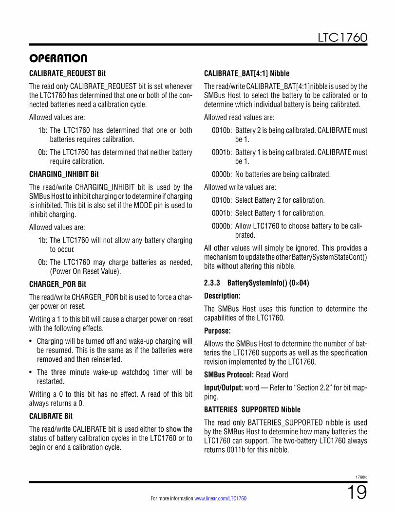
OPERATIONCALIBRATE_REQUEST Bit
The read only CALIBRATE_REQUEST bit is set whenever the LTC1760 has determined that one or both of the con-nected batteries need a calibration cycle.
Allowed values are:
1b: The LTC1760 has determined that one or both batteries requires calibration.
0b: The LTC1760 has determined that neither battery require calibration.
CHARGING_INHIBIT Bit
The read/write CHARGING_INHIBIT bit is used by the SMBus Host to inhibit charging or to determine if charging is inhibited. This bit is also set if the MODE pin is used to inhibit charging.
Allowed values are:
1b: The LTC1760 will not allow any battery charging to occur.
0b: The LTC1760 may charge batteries as needed, (Power On Reset Value).
CHARGER_POR Bit
The read/write CHARGER_POR bit is used to force a char-ger power on reset.
Writing a 1 to this bit will cause a charger power on reset with the following effects.
• Charging will be turned off and wake-up charging will be resumed. This is the same as if the batteries were removed and then reinserted.
• The three minute wake-up watchdog timer will be restarted.
Writing a 0 to this bit has no effect. A read of this bit always returns a 0.
CALIBRATE Bit
The read/write CALIBRATE bit is used either to show the status of battery calibration cycles in the LTC1760 or to begin or end a calibration cycle.
CALIBRATE_BAT[4:1] Nibble
The read/write CALIBRATE_BAT[4:1]nibble is used by the SMBus Host to select the battery to be calibrated or to determine which individual battery is being calibrated.
Allowed read values are:
0010b: Battery 2 is being calibrated. CALIBRATE must be 1.
0001b: Battery 1 is being calibrated. CALIBRATE must be 1.
0000b: No batteries are being calibrated.
Allowed write values are:
0010b: Select Battery 2 for calibration.
0001b: Select Battery 1 for calibration.
0000b: Allow LTC1760 to choose battery to be cali-brated.
All other values will simply be ignored. This provides a mechanism to update the other BatterySystemStateCont() bits without altering this nibble.
2.3.3 BatterySystemInfo() (0×04)
Description:
The SMBus Host uses this function to determine the capabilities of the LTC1760.
Purpose:
Allows the SMBus Host to determine the number of bat-teries the LTC1760 supports as well as the specification revision implemented by the LTC1760.
SMBus Protocol: Read Word
Input/Output: word — Refer to “Section 2.2” for bit map-ping.
BATTERIES_SUPPORTED Nibble
The read only BATTERIES_SUPPORTED nibble is used by the SMBus Host to determine how many batteries the LTC1760 can support. The two-battery LTC1760 always returns 0011b for this nibble.

LTC1760
201760fc
For more information www.linear.com/LTC1760
BATTERY_SYSTEM_REVISION Nibble
The read only BATTERY_SYSTEM_REVISION nibble re-ports the version of the Smart Battery System Manager specification supported.
LTC1760 always returns 1000b for this nibble, indicating Version 1.0 without optional PEC support.
2.3.4 LTC() (0×3C)
Description:
This function returns the LTC version nibble and allows the user to perform expanded Smart Battery System Manager functions.
Purpose:
Used by the SMBus Host to determine the version of the LTC1760 and to program and monitor TURBO and POWER_OFF special functions.
SMBus Protocol: Read or Write Word.
Input/Output: word — Refer to “Section 2.2” for bit map-ping.
POWER_OFF Bit
This read/write bit allows the LTC1760 to turn off all power paths.
Allowed values:
1b: All power paths are off.
0b: All power paths are enabled. (power on reset value).
TURBO Bit
This read/write bit allows the LTC1760 to enter TURBO charging mode. Refer to “section 3.6”.
Allowed values:
1b: Turbo charging mode enabled.
0b: Turbo charging mode disabled. (Power On Reset Value).
LTC_Version[3:0] Nibble
This read only nibble always returns 0001b as the LTC1760 version.
OPERATION2.3.5 BatteryMode() (0×03)
Description:
This function is used by the LTC1760 to read the battery’s Mode register.
Purpose:
Allows the LTC1760 to determine if a battery requires a conditioning/calibration cycle.
SMBus Protocol: Read Word. LTC1760 reads Battery 1 or Battery 2 as an SMBus Master.
Input/Output: word — Refer to “Section 2.2” for bit map-ping.
CONDITION_FLAG Bit
The CONDITION_FLAG bit is set whenever the battery requires calibration.
Allowed values:
1b: Battery requires calibration. (Also known as a Condition Cycle Request).
0b: Battery does not require calibration.
2.3.6 Voltage() (0×09)
Description:
This function is used by the LTC1760 to read the actual cell-pack voltage .
Purpose:
Allows the LTC1760 to determine the cell pack voltage and close the charging voltage servo loop.
SMBus Protocol: Read Word. LTC1760 reads Battery 1 or Battery 2 as an SMBus Master.
Output: unsigned integer — battery terminal voltage in milli-volts. Refer to “Section 2.2” for bit mapping.
Units: mV.
Range: 0 to 65,535 mV.

LTC1760
211760fc
For more information www.linear.com/LTC1760
2.3.7 Current() (0×0A)
Description:
This function is used by the LTC1760 to read the actual current being supplied through the battery terminals.
Purpose:
Allows the LTC1760 to determine how much current a battery is receiving through its terminals and close the charging current servo loop.
SMBus Protocol: Read Word. LTC1760 reads Battery 1 or Battery 2 as an SMBus Master.
Output: signed integer (2’s complement) — charge/dis-charge rate in mA increments - positive for charge, nega-tive for discharge. Refer to “Section 2.2” for bit mapping.
Units: mA.
Range: 0 to 32,767 mA for charge or 0 to -32,768 mA for discharge.
2.3.8 ChargingCurrent() (0×14)
Description:
This function is used by the LTC1760 to read the Smart Battery’s desired charging current.
Purpose:
Allows the LTC1760 to determine the maximum charging current.
SMBus Protocol: Read Word. LTC1760 reads Battery 1 or Battery 2 as an SMBus Master.
Output: unsigned integer — maximum charger output current in mA. Refer to “Section 2.2” for bit mapping.
Units: mA.
Range: 0 to 65,534 mA.
2.3.9 ChargingVoltage() (0×15)
Description:
This function is used by the LTC1760 to read the Smart Battery’s desired charging voltage.
Purpose:
Allows the LTC1760 to determine the maximum charging voltage.
SMBus Protocol: Read Word. LTC1760 reads Battery 1 or Battery 2 as an SMBus Master.
Output: unsigned integer — charger output voltage in mV. Refer to “Section 2.2” for bit mapping.
Units: mV.
Range: 0 to 65,534 mV.
2.3.10 AlarmWarning() (0×16)
Description:
This function is used by the LTC1760 to read the Smart Battery’s Alarm register.
Purpose:
Allows the LTC1760 to determine the state of all applicable alarm flags.
SMBus Protocol: Read Word. LTC1760 reads Battery 1 or Battery 2 as an SMBus Master.
Output: unsigned integer – Refer to “Section 2.2” for bit mapping.
OVER_CHARGED_ALARM Bit
The read only OVER_CHARGED_ALARM bit is used by the LTC1760 to determine if charging may continue.
Allowed values are:
1b: The LTC1760 will not charge this battery.
0b: The LTC1760 may charge this battery if other conditions permit charging.
TERMINATE_CHARGE_ALARM Bit
The read only TERMINATE_CHARGE_ALARM bit is used by the LTC1760 to determine if charging may continue.
Allowed values are:
1b: The LTC1760 will not charge this battery.
0b: The LTC1760 may charge this battery if other conditions permit charging.
OPERATION

LTC1760
221760fc
For more information www.linear.com/LTC1760
TERMINATE_CHARGE_RESERVED BitThe read only TERMINATE_CHARGE_RESERVED bit is used by the LTC1760 to determine if charging may continue. Allowed values are:
1b: The LTC1760 will not charge this battery.
0b: The LTC1760 may charge this battery if other conditions permit charging.
OVER_TEMP_ALARM BitThe read only OVER_TEMP_ALARM bit is used by the LTC1760 to determine if charging may continue.
Allowed values are:
1b: The LTC1760 will not charge this battery.
0b: The LTC1760 may charge this battery if other conditions permit charging.
TERMINATE_DISCHARGE_ALARM BitThe read only TERMINATE_DISCHARGE_ALARM bit is used by the LTC1760 to determine if discharge from the battery is still allowed. This is used for PowerPath man-agement and battery calibration.
Allowed values are:
1b: The LTC1760 will terminate calibration and should try to not use this battery in the power path. When all other power paths fail the LTC1760 will ignore this alarm and still try to supply system power from this battery.
0b: The LTC1760 may continue discharging this battery.
FULLY_DISCHARGED BitThe read only FULLY_DISCHARGED bit is used by the LTC1760 to determine if discharge from the battery is still allowed. This is used for PowerPath management and battery calibration.
Allowed values are:
1b: The LTC1760 will terminate calibration and should try to not use this battery in the power path. When all other power paths fail the LTC1760 will ignore this alarm and still try to supply system power from this battery.
0b: The LTC1760 may continue discharging this battery.
OPERATION2.3.11 AlertResponse()
Description:The SMBus Host uses the Alert Response Address (ARA) to simultaneously address all devices on the SMBus and de-termine which devices are currently asserting SMBALERT.Purpose:This command allows the SMBus Host to identify the subset of devices that have new status data. This reduces the number of reads required to refresh all status infor-mation from the system. The SMBus Host begins an ARA by transmitting the 8-bit address, 0×18, to all devices. ARA-compliant devices that are asserting SMBALERT will then simultaneously return their address on the next read byte. While transmitting their address each device monitors SDA. If a lower address is present, the device transmitting the higher address will see that SDA does not match and it will stop transmitting its address. When a device sees its full address has been received it will stop asserting SMBALERT and the Host will know to read status from this device. Subsequent ARA requests will allow the Host to complete the list of devices requiring servicing.
Output:The LTC1760 will transmit its 8-bit address, 0x14, in response to an ARA request. The LTC1760 will stop trans-mitting its address if another device with a lower address is also responding to the ARA. The LTC1760 will de-assert SMBALERT when it successfully returns its address.
The following events will cause the LTC1760 to pull-down the SMBALERT# bus through the SMBALERT pin:
• Change of AC_PRESENT in the BatterySystemSta-teCont() function.
• Change of BATTERY_PRESENT in the BatterySys-temState() function.
• Internal power on reset condition.
Refer to “Section 2.2” for bit mapping.
2.4 SMBus Dual Port Operation
The SMBus Interface includes the LTC1760’s SMBus controller, as well as circuitry to arbitrate and connect the battery and SMBus Host interfaces. The SMBus controller generates and interprets all LTC1760 SMBus functions.

LTC1760
231760fc
For more information www.linear.com/LTC1760
OPERATION
HOSTSMB*
SMB1*
SMB2*BAT2
BAT1
HOST, LTC1760 AND BAT1 CAN COMMUNICATE.BAT2 ORIGINATED COMMANDS ARE IGNORED.
HOSTSMB*
SMB1*
SMB2*BAT2
BAT1
LTC1760 AND BAT2 CAN COMMUNICATE. HOST ANDBAT1 ORIGINATED COMMANDS ARE STRETCHED IF THE LTC1760 IS COMMUNICATING WITH BAT2.
LTC1760 AND BAT1 CAN COMMUNICATE. HOST ANDBAT2 ORIGINATED COMMANDS ARE STRETCHED IF THE LTC1760 IS COMMUNICATING WITH BAT1.
HOSTSMB*
SMB1*
SMB2*BAT2
BAT1
HOST, LTC1760 AND BAT2 CAN COMMUNICATE.BAT1 ORIGINATED COMMANDS ARE IGNORED.
HOSTSMB*
SMB1*
SMB2*BAT2
BAT1
(1b)(1a)
(1d)(1c)1760 F01
*SMB INCLUDES SCL AND SDA, SMB1 INCLUDES SCL1 AND SDA1, AND SMB2 INCLUDES SCL2 AND SDA2.
LTC1760SMBus
CONTROLLER
LTC1760SMBus
CONTROLLER
LTC1760SMBus
CONTROLLER
LTC1760SMBus
CONTROLLER
Figure 1. Switch Configurations Used by the LTC1760 for Managing Dual Port Battery Communication
The dual port operation allows the SMBus Host to be connected to the SMBus of either battery by setting the SMB_BAT[4:1] nibble. Arbitration is handled by stretching an SMBus start sequence when a bus collision might occur. Whenever configurations are switched, the LTC1760 will generate a harmless SMBus reset on SMB1 and SMB2 as required. The four possible configurations are illustrated in Figure 1. Sample SMBus communications are shown in Figures 2 and 3.
2.5 LTC1760 SMBus Controller Operation
SMBus communication with the LTC1760 is handled by the SMBus Controller, a sub-block of the SMBus Interface. Data is clocked into the SMBus Controller block shift register after the rising SCL edge. Data is clocked out of the SMBus Control block shift register after the falling edge of SCL.
The LTC1760 acting as a Slave will acknowledge (ACK) each byte of serial data. The Command byte will be NACKed if
an invalid command code is transmitted to the LTC1760. The SMBus Controller must respond if addressed as a combined Smart Battery System Manager at 8-bit address 0×14. A valid address includes a legal Read/Write bit. The SMBus Controller will ignore invalid data although the data transmission with the invalid data will still be ACKed.
When the LTC1760, acting as a bus Master receives a NACK, it will terminate the transmission and provide a STOP condition on the bus.
Detection of a STOP condition, power on reset, or SMBus time out will reset the Controller to an initial state at any time.
The LTC1760 supports ARA, Write Word and Read Word protocols as an SMBus Slave. The LTC1760 supports Read Word protocol as an SMBus Master.
Refer to “System Management Bus Specification” for a complete description of required operation and symbols.

LTC1760
241760fc
For more information www.linear.com/LTC1760
OPERATION
SMBu
s DU
ALPO
RT
SCL
SDA
SCL1
SDA1
SCL2
SDA2
Figu
re 2
. LTC
1760
Stre
tche
s Ho
st’s
Com
mun
icat
ion
With
Bat
tery
1 W
hile
It C
ompl
etes
a R
ead
Of B
atte
ry 2
. (Co
nfig
urat
ion
b)

LTC1760
251760fc
For more information www.linear.com/LTC1760
OPERATION
SMBu
s DU
AL P
ORT
SCL
SDA
SCL1
SDA1
SCL2
SDA2
Figu
re 3
. LTC
1760
Que
ries
Batte
ry 1
Fol
low
ed B
y Ba
ttery
2 F
or R
eque
sted
Cur
rent
. (Co
nfig
urat
ion
b)
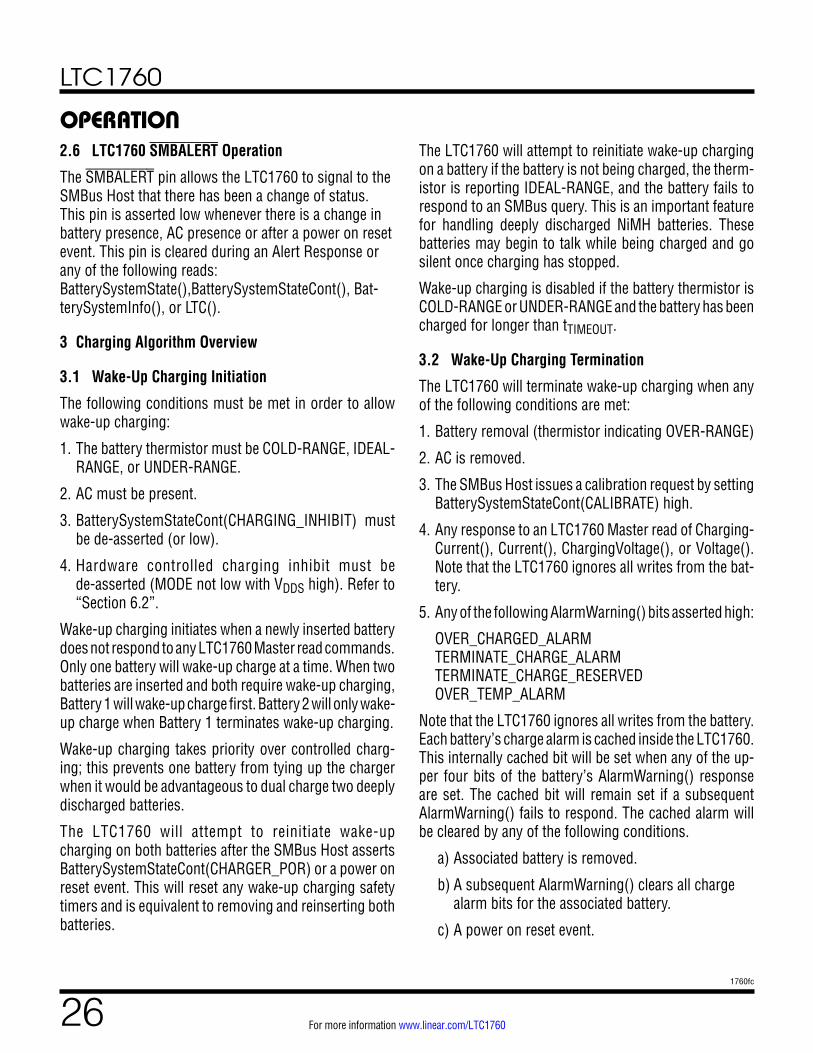
LTC1760
261760fc
For more information www.linear.com/LTC1760
OPERATION2.6 LTC1760 SMBALERT Operation
The SMBALERT pin allows the LTC1760 to signal to the SMBus Host that there has been a change of status. This pin is asserted low whenever there is a change in battery presence, AC presence or after a power on reset event. This pin is cleared during an Alert Response or any of the following reads: BatterySystemState(),BatterySystemStateCont(), Bat-terySystemInfo(), or LTC().
3 Charging Algorithm Overview
3.1 Wake-Up Charging Initiation
The following conditions must be met in order to allow wake-up charging:
1. The battery thermistor must be COLD-RANGE, IDEAL-RANGE, or UNDER-RANGE.
2. AC must be present.
3. BatterySystemStateCont(CHARGING_INHIBIT) must be de-asserted (or low).
4. Hardware controlled charging inhibit must be de-asserted (MODE not low with VDDS high). Refer to “Section 6.2”.
Wake-up charging initiates when a newly inserted battery does not respond to any LTC1760 Master read commands. Only one battery will wake-up charge at a time. When two batteries are inserted and both require wake-up charging, Battery 1 will wake-up charge first. Battery 2 will only wake-up charge when Battery 1 terminates wake-up charging.
Wake-up charging takes priority over controlled charg-ing; this prevents one battery from tying up the charger when it would be advantageous to dual charge two deeply discharged batteries.
The LTC1760 will attempt to reinitiate wake-up charging on both batteries after the SMBus Host asserts BatterySystemStateCont(CHARGER_POR) or a power on reset event. This will reset any wake-up charging safety timers and is equivalent to removing and reinserting both batteries.
The LTC1760 will attempt to reinitiate wake-up charging on a battery if the battery is not being charged, the therm-istor is reporting IDEAL-RANGE, and the battery fails to respond to an SMBus query. This is an important feature for handling deeply discharged NiMH batteries. These batteries may begin to talk while being charged and go silent once charging has stopped.
Wake-up charging is disabled if the battery thermistor is COLD-RANGE or UNDER-RANGE and the battery has been charged for longer than tTIMEOUT.
3.2 Wake-Up Charging Termination
The LTC1760 will terminate wake-up charging when any of the following conditions are met:
1. Battery removal (thermistor indicating OVER-RANGE)
2. AC is removed.
3. The SMBus Host issues a calibration request by setting BatterySystemStateCont(CALIBRATE) high.
4. Any response to an LTC1760 Master read of Charging-Current(), Current(), ChargingVoltage(), or Voltage(). Note that the LTC1760 ignores all writes from the bat-tery.
5. Any of the following AlarmWarning() bits asserted high:
OVER_CHARGED_ALARM TERMINATE_CHARGE_ALARM TERMINATE_CHARGE_RESERVED OVER_TEMP_ALARM
Note that the LTC1760 ignores all writes from the battery. Each battery’s charge alarm is cached inside the LTC1760. This internally cached bit will be set when any of the up-per four bits of the battery’s AlarmWarning() response are set. The cached bit will remain set if a subsequent AlarmWarning() fails to respond. The cached alarm will be cleared by any of the following conditions.
a) Associated battery is removed.
b) A subsequent AlarmWarning() clears all charge alarm bits for the associated battery.
c) A power on reset event.

LTC1760
271760fc
For more information www.linear.com/LTC1760
d) The SMBus Host asserts BatterySystemStateCont(CHARGER_POR) high.
6. The SMBus Host asserts BatterySystemStateCont(CHARGING_INHIBIT) high.
7. Hardware controlled charging inhibit is asserted (MODE low with VDDS high). Refer to “Section 6.2”.
8. The thermistor of the battery being charged indicates COLD-RANGE and the battery has been charged for longer than tTIMEOUT.
9. The thermistor of the battery being charged indicates UNDER-RANGE and the battery has been charged for longer than tTIMEOUT.
10. The thermistor of the battery being charged indicates HOT-RANGE.
11. Any SMBus communication line is held low for longer than tQUERY.
12. BatterySystemStateCont(POWER_NOT_GOOD) is high.
13. The emergency turn-off feature has been asserted using the DCDIV input pin.
3.3 Wake-Up Charging Current and Voltage Limits
The wake-up charging current is fixed at IWAKE_UP for all values of ILIMIT. Wake-up charging uses the low current mode described in “Section 10”.
The wake-up charging voltage is not limited by the VLIMIT function.
3.4 Controlled Charging Initiation
All of the following conditions must be met in order to allow controlled charging of a given battery. One or both batteries may be controlled charged at a time.
1. The battery thermistor must be COLD-RANGE, IDEAL-RANGE, or UNDER-RANGE.
2. AC must be present.
3. BatterySystemStateCont(CHARGING_INHIBIT) must be de-asserted (or low).
4. Hardware controlled charging inhibit must be de-asserted (MODE not low with VDDS high). Refer to “Section 6.2”.
5. The battery responds to an LTC1760 Master read of Alarm() with all charge alarms deasserted.
6. The battery responds to an LTC1760 Master read of ChargingVoltage() with a non zero voltage request value.
7. The battery responds to an LTC1760 Master read of Voltage().
8. The battery responds to an LTC1760 Master read of ChargingCurrent() with a non zero current request value.
9. The battery responds to an LTC1760 Master read of Current().
The following charging related functions are polled each tQUERY: Alarm(), ChargingVoltage(), Voltage(), Charging-Current(), and Current().
3.5 Controlled Charging Termination
The LTC1760 will terminate controlled charging when any of the following conditions are met:
1. Battery removal, or thermistor indicating OVER-RANGE.
2. AC removal.
3. The SMBus Host issues a calibration request by setting BatterySystemStateCont(CALIBRATE) high.
4. An LTC1760 Master read of ChargingCurrent() returning a zero current request.
5. An LTC1760 Master read of ChargingVoltage() returning a zero voltage request.
6. Any of the following AlarmWarning() bits asserted high:
OVER_CHARGED_ALARM TERMINATE_CHARGE_ALARM TERMINATE_CHARGE_RESERVED OVER_TEMP_ALARM
Note that the LTC1760 ignores all writes from the battery. Each battery’s charge alarm is cached inside the LTC1760. This internally cached bit will be set when any of the upper four bits of the battery’s AlarmWarning() response are set.
OPERATION

LTC1760
281760fc
For more information www.linear.com/LTC1760
This cached bit will remain set if a subsequent AlarmWarn-ing() fails to respond. The cached alarm will be cleared by any of the following conditions.
a) Associated battery is removed.
b) A subsequent AlarmWarning() clears all charge alarm bits for the associated battery.
c) A power on reset event.
d) The SMBus Host asserts BatterySystemStateCont(CHARGER_POR) high.
7. The SMBus Host asserts BatterySystemStateCont(CHARGING_INHIBIT) high.
8. Hardware controlled charging inhibit is asserted (MODE low with VDDS high).
9. The SMBus of the battery being charged has stopped acknowledging SMBus read commands for longer than tTIMEOUT.
10. The thermistor of the battery being charged indicates HOT-RANGE.
11. Any SMBus communication line is grounded for longer than tQUERY.
12. BatterySystemStateCont(POWER_NOT_GOOD) is high.
13. The emergency turn-off feature has been asserted using the DCDIV input pin.
Whenever changing conditions cause either battery to stop charging, charging is stopped immediately for all batteries and the voltage and current algorithms are reset to zero. Charging is not resumed until all the conditions for controlled charging are met.
3.6 Controlled Charging Current Programming
The LTC1760 uses a single charger stage to simultaneously charge up to two batteries. The batteries are connected to the charger using a charge MUX. The charge MUX allows the total charger current to be shared by the two batteries while preventing charge transfer between the batteries. Refer to “Section 7.1” and “Section 7.2”.
When charging a single battery, the charging algorithm attempts to adjust the current so as to match the reported current with the requested current. The LTC1760 con-tinuously adjusts the charging current by the difference between the actual and requested currents.
When simultaneously charging two batteries, the charging algorithm attempts to adjust the current so as to match the reported current with the requested current in both batteries. The LTC1760 calculates the difference between the requested and actual current in both batteries and uses the minimum of these differences to increment or decrement the total charge current being provided by the charging stage.
The charging algorithm will not allow the reported actual current to exceed the requested current in either battery. For this reason the most efficient charging occurs for matched batteries at similar charge states.
Whenever changing conditions cause either battery to stop charging, the current algorithm is reset to zero. The programmed current is updated every tQUERY.
There are additional safety restrictions that limit the total output current of the charger. These are detailed in the following three sub-sections.
3.6.1 Current Limits When Charging A Single Battery
The following additional limits are applied to the charg-ing current algorithm described in 3.6 when charging a single battery:
a) The programmed current cannot exceed the re-quested current + ILIMIT/32.
b) The programmed current cannot exceed ILIMIT.
3.6.2 Current Limits When Charging Two Batteries (TURBO Mode Disabled)
The following additional limits are applied to the charging current algorithm described in 3.6 when charging two batteries with turbo mode disabled:
a) The programmed current cannot exceed the maxi-mum of the two requested currents + ILIMIT/32.
b) The programmed current cannot exceed ILIMIT.
OPERATION

LTC1760
291760fc
For more information www.linear.com/LTC1760
3.6.3 Current Limits When Charging Two Batteries (TURBO Mode Enabled)
The following additional limits are applied to the charging current algorithm described in 3.6 when charging two batteries with turbo mode enabled:
a) The programmed current cannot exceed the maxi-mum of the two requested currents + ILIMIT. This relaxed limit enables accelerated charging if ILIMIT is greater than the maximum of the two requested currents. For the recommended matched battery pair the requested current should be the same.
b) The programmed current cannot exceed ILIMIT
TURBO mode provides a mechanism for the SMBus Host to enable the charge MUX to apply additional current to both batteries. TURBO mode only has an effect when two batteries are being charged simultaneously. TURBO mode does not affect wake-up charging or any other conditions that could inhibit charging. TURBO mode is entered when LTC(TURBO) is set high.
Normally the LTC1760 will limit the current into both bat-teries to the maximum of the two requested currents + ILIMIT/32. TURBO mode removes this restriction, allowing the charger to output as much as ILIMIT into the combined battery system.
For example: In a system where LTC(TURBO)=0, ILIMIT=4.0A and each battery is requesting 2A the LTC1760 will not output more than 2.125A into the combined battery system or 1.06A into each battery if their charge states match. In a system where LTC(TURBO)=1, ILIMIT= 4.0A and each battery is requesting 2A the LTC1760 will now output up to ILIMIT into the combined battery system or 2A into each battery if their charge states match.
Even without TURBO mode, the LTC1760 offers signifi-cantly reduced charge times for matched batteries in the top-off state. This time savings is especially significant for Lithium-Ion batteries. Simultaneously charging two bat-teries reduces losses in switches and improves efficiency.
3.7 Controlled Charging Voltage Programming
The LTC1760 monitors the requested and actual voltages in each battery and increments the programmed voltage
by 16mV each tQUERY unless one of the following condi-tions are met:
a) The actual voltage exceeds the requested voltage in either battery.
b) The actual voltage exceeds VLIMIT.
This is an extremely important feature of the LTC1760 since it allows the charger to servo on the internal cell voltage of the battery as determined by the Smart Battery. This voltage may be significantly lower than the battery pack terminal voltage which is used by all Level 2 chargers. The advantage for the LTC1760 is improved charge time, safety, and a more completely charged battery.
The voltage correction cannot exceed the minimum re-quested voltage by more than 512mV. When decrementing, the programmed voltage is reduced by 16mV each tQUERY. Whenever changing conditions cause either battery to stop charging, the voltage algorithm is reset to zero.
4 System Power Management Algorithm and Battery Calibration
4.1 Turning Off System Power
The LTC1760 allows the user to turn off system power using the LTC(POWER_OFF) bit. When POWER_OFF is asserted high all power management functions are bypassed and the LTC1760 will turn off DCIN, BAT2 and BAT1 power paths. This feature allows the user to power down the system. Charging is still allowed when POWER_OFF is asserted high.
4.2 Power-By Algorithm When No Battery is Being Calibrated
The LTC1760 will always attempt to maintain system power. The preferred configuration is to remain in 3- Diode mode. In 3-Diode mode, power will be provided by BAT1, BAT2 and DCIN with the source at the highest voltage potential automatically providing all the power. Sources at similar voltage potentials will share power based on their capacity.
The following conditions will cause the LTC1760 to modify its preferred power-by algorithm.
OPERATION

LTC1760
301760fc
For more information www.linear.com/LTC1760
Power Reporting for Batteries Being Calibrated
AC_PRESENT CALIBRATE_BAT2 CALIBRATE_BAT1POWERED_BY_BAT(4:1)
1 0 0 0000b
1 1 1 0001b
1 1 0 0010b
*States not shown are not allowed
Power Reporting as a Function of Battery Presence
AC_PRESENT PRESENT_BAT2 PRESENT_BAT1POWERED_BY_BAT(4:1)
1 X X 0000b
0 0 0 0000b
0 0 1 0001b
0 1 0 0010b
0 1 1 0011b
Power Reporting with AC_PRESENT Low and both Batteries Present, as a Function of Power Alarms.
AC_PRESENT
BATTERY 2 POWER ALARM
(NOTE 1)
BATTERY 1 POWER ALARM
(NOTE 1)POWERED_BY_BAT(4:1)
0 0 0 0011b
0 0 1 0010b
0 1 0 0001b
0 1 1 0011b
1 X X 0000bNote 1: A power alarm means that ALARM() has returned TERMINATE_DISCHARGE=1 or FULLY_DISCHARGED_ALARM=1
Power Reporting When BatterySystemStateCont(POWER_NOT_GOOD) is High and the LTC1760 has Autonomously Entered 3-Diode Mode
AC_PRESENT PRESENT_BAT2 PRESENT_BAT1POWERED_BY_BAT(4:1)
0 0 0 0000b
0 0 1 0001b
0 1 0 0010b
0 1 1 0011b
1 0 0 0000b
1 0 1 0000b
1 1 0 0000b
1 1 1 0000b
OPERATION1. A battery issues a TERMINATE_DISCHARGE alarm and
AC_PRESENT is high. The LTC1760 will select the other battery and DCIN to power the system.
2. A battery issues a TERMINATE_DISCHARGE alarm and AC_PRESENT is low. The LTC1760 will select the other battery to power the system.
3. A battery issues a TERMINATE_DISCHARGE alarm, AC_PRESENT is low, and the other battery is not present or has previously issued an alarm. The LTC1760 will autonomously try to restore power by entering 3-Diode mode. The 3-Diode mode will ignore TERMINATE_DISCHARGE and FULLY_DISCHARGED alarms.
4.3 Power-By Algorithm When a Battery is Being Calibrated
During battery calibration, the battery being calibrated is the only device powering the system. This will be reflected in the reported POWER_BY[4:1] bits. See “Section 5” for more information on battery calibration.
4.4 Power-By Reporting
The following tables illustrate how BatterySystem State(POWER_BY_BAT[4:1]) interprets PowerPath conditions. 5 Battery Calibration (Conditioning)
Calibration allows the SMBus Host to fully discharge a battery for conditioning purposes. The SMBus Host may determine the battery to be discharged or allow the LTC1760 to choose based on the batteries’ request to be conditioned.
5.1 Selecting a Battery to be Calibrated
Option 1) SMBus Host chooses battery to be calibrated using BatterySystemStateCont(CALIBRATE_BAT[4:1])
Allowed values:
0001b: Set CALIBRATE_BAT1. Only has an effect if Battery 1 BatteryMode(CONDITION_FLAG) is high . May not be updated if a calibration is in progress.
0010b: Set CALIBRATE_BAT2. Only has an effect if Battery 2 BatteryMode(CONDITION_FLAG) is high. May not be updated if a calibration is in progress.

LTC1760
311760fc
For more information www.linear.com/LTC1760
0000b: Clears CALIBRATE_BAT1 and CALIBRATE_BAT2 and allows LTC1760 to chose. Power on reset default. May not be updated if a calibration is in progress.
Option 2) SMBus Host allows LTC1760 to choose battery to be calibrated.
BatterySystemStateCont(CALIBRATE_BAT[4:1]) = 0000b. See previous option.
The LTC1760 determines that the battery requires calibration by reading BatteryMode(CONDITION_FLAG). This flag is cached in the LTC1760. The LTC1760 sets BatterySystemStateCont(CALIBRATE_REQUEST) high. The LTC1760 will always select the battery that is requesting calibration. If both batteries are requesting calibration, the LTC1760 will select Battery 1. If neither battery is request-ing calibration, then calibration cannot occur.
5.2 Initiating Calibration of Selected Battery
The SMBus Host initiates a calibration by writing to Batt erySystemStateCont(CALIBRATE). Follow rules of the previous section to preserve battery intended for calibra-tion. The SMBus Host must only set the calibration bit once per calibration.
The LTC1760 will discharge the selected battery as long as the calibration is in progress (CALIBRATE high). Updates to the cached BatteryMode(CONDITION_FLAG) will be inhibited while CALIBRATE is asserted. This means that discharge of the battery will continue even if the battery clears the CONDITION_FLAG.
5.3 Terminating Calibration of Selected Battery
Calibration will end when CALIBRATE is cleared. CALI-BRATE will be cleared when:
• AC is removed.
• The battery being calibrated is removed. When the battery being calibrated is removed, the LTC1760 will automatically calibrate the other battery if it is request-ing calibration.
• BatterySystemStateCont(POWER_NOT_GOOD) is high.
Summary of SDA, SCL and SMBALERT Operation as a Function of MODE and VDDS LevelsCONDITION LTC1760 OPERATING MODE
VMODE = GND VVDDS < VIL_VDDS
SCL: Clock for Status Indicators SCL: Clock for Status Indicators SDA: Battery 2 Status SMBALERT: Battery 1 Status
VMODE = GND VVDDS > VIH_VDDS
SCL, SDA, SMBALERT: Normal Operation LTC1760 Charging Inhibited
VMODE = VVCC2 VVDDS < VIL_VDDS
SCL, SDA Ignored and May Float Low SMBALERT: Normal Operation SCL1, SDA1, SCL2 and SDA2: Normal Operation and Charging is Allowed
VMODE = VVCC2 VVDDS > VIH_VDDS
Normal Operation on all Pins, Charging is Allowed
• The battery sets Alarm Warning(TERMINATE_DISCHARGE) high.
• The battery sets Alarm Warning (FULLY_DISCHARGED) high.
• A zero is written to the CALIBRATE bit.
The LTC1760 will attempt to initiate a charge cycle after the discharge cycle is completed.
6 MODE Pin Operation
The MODE pin is a multifunction pin that allows the LTC1760 to: 1) display charging status in stand alone operation; 2) activate hardware charge inhibit; 3) charge when SCL and SDA are low and; 4) charge with an SMBus Host.
OPERATION
6.1 Standalone Charge Indication
When MODE is tied to GND and VVDDS < VIL_VDDS, the function of SDA, SMBALERT, and SCL are changed as described below:
SDA is an output and is used to monitor charging status of Battery 2. Allowed values are:
Low: Battery 2 is charging.
High: Battery 2 not charging (AC is not present or bat-tery is not present).
Blinking: Battery 2 charge complete (AC is present, battery is present and not charging).

LTC1760
321760fc
For more information www.linear.com/LTC1760
SMBALERT is used to monitor charging status of Battery 1. Allowed values are:
Low: Battery 1 is charging.
High: Battery 1 not charging (AC is not present or bat-tery is not present).
Blinking: Battery 1 charge complete (AC is present, battery is present and not charging).
SCL is an input and is used to determine the blinking rate of SDA and SMBALERT. Tie SCL high if blinking is not desired. This will provide two different states to indicate charging (output low) and not charging (output high).
6.2 Hardware Charge Inhibit
When MODE is tied to GND and VVDDS>VIH_VDDS, charging is inhibited and BatterySystemStateCont(CHARGING_INHIBIT) will report a logic high.
6.3 Charging When SCL And SDA Are Low
When MODE is tied to VCC2 and VVDDS < VIL_VDDS, SDA and SCL are not used and will not interfere with LTC1760 battery communication. This feature allows the LTC1760 to autonomously charge when SCL and SDA are not available. This scenario might occur when SMBus Host has powered down and is no longer pulling up on SCL and SDA.
6.4 Charging With an SMBus Host
When Mode is tied to VCC2 and VVDDS > VIH_VDDS, SDA and SCL are used to communicate with the SMBus Host.
7 Battery Charger Controller
The LTC1760 charger controller uses a constant off-time, current mode step-down architecture. During normal operation, the top MOSFET is turned on each cycle when the oscillator sets the SR latch and turned off when the main current comparator ICMP resets the SR latch. While the top MOSFET is off, the bottom MOSFET is turned on until either the inductor current trips the current compara-tor IREV, or the beginning of the next cycle. The oscillator uses the equation:
tOFF = (VDCIN - VBAT)/(VDCIN • fOSC)
OPERATION
TGATE
BGATE
ON
ON
OFF
OFF
tOFF
TRIP POINT SET BY ITH VOLTAGE
INDUCTORCURRENT
1760 F04
Figure 4.
to set the bottom MOSFET on time. The result is quasi-constant frequency operation where the converter fre-quency remains nearly constant over a wide range of output voltages. This activity is diagrammed in Figure 4.
The peak inductor current, at which ICMP resets the SR latch, is controlled by the voltage on ITH. ITH is in turn controlled by several loops, depending upon the situation at hand. The average current control loop converts the voltage between CSP and BAT to a representative current. Error amp CA2 compares this current against the desired current programmed by the IDAC at the ISET pin and adjusts ITH for the desired voltage across RSENSE.
The voltage at BAT is divided down by an internal resis-tor divider set by the VDAC and is used by error amp EA to decrease ITH if the divider voltage is above the 0.8V reference.
The amplifier CL1 monitors and limits the input current, normally from the AC adapter, to a preset level (100 mV/RCL). At input current limit, CL1 will decrease the ITH volt-age and thus reduce battery charging current.
An over-voltage comparator, OV, guards against transient overshoots (>7.5%). In this case, the top MOSFET is turned off until the over-voltage condition is cleared. This feature is useful for batteries which “load dump” themselves by opening their protection switch to perform functions such as calibration or pulse-mode charging.
The top MOSFET driver is powered from a floating boot-strap capacitor C4. This capacitor is normally recharged from VCC through an external diode when the top MOS-FET is turned off. As VIN decreases towards the selected
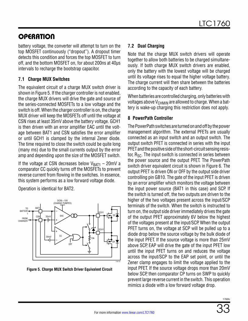
LTC1760
331760fc
For more information www.linear.com/LTC1760
battery voltage, the converter will attempt to turn on the top MOSFET continuously (“dropout’’). A dropout timer detects this condition and forces the top MOSFET to turn off, and the bottom MOSFET on, for about 200ns at 40µs intervals to recharge the bootstrap capacitor.
7.1 Charge MUX Switches
The equivalent circuit of a charge MUX switch driver is shown in Figure 5. If the charger controller is not enabled, the charge MUX drivers will drive the gate and source of the series-connected MOSFETs to a low voltage and the switch is off. When the charger controller is on, the charge MUX driver will keep the MOSFETs off until the voltage at CSN rises at least 35mV above the battery voltage. GCH1 is then driven with an error amplifier EAC until the volt-age between BAT1 and CSN satisfies the error amplifier or until GCH1 is clamped by the internal Zener diode. The time required to close the switch could be quite long (many ms) due to the small currents output by the error amp and depending upon the size of the MOSFET switch.
If the voltage at CSN decreases below VBAT1 – 20mV a comparator CC quickly turns off the MOSFETs to prevent reverse current from flowing in the switches. In essence, this system performs as a low forward voltage diode.
Operation is identical for BAT2.
7.2 Dual Charging
Note that the charge MUX switch drivers will operate together to allow both batteries to be charged simultane-ously. If both charge MUX switch drivers are enabled, only the battery with the lowest voltage will be charged until its voltage rises to equal the higher voltage battery. The charge current will then share between the batteries according to the capacity of each battery.
When batteries are controlled charging, only batteries with voltages above VCHMIN are allowed to charge. When a bat-tery is wake-up charging this restriction does not apply.
8 PowerPath Controller
The PowerPath switches are turned on and off by the power management algorithm. The external PFETs are usually connected as an input switch and an output switch. The output switch PFET is connected in series with the input PFET and the positive side of the short-circuit sensing resis-tor, RSC. The input switch is connected in series between the power source and the output PFET. The PowerPath switch driver equivalent circuit is shown in Figure 6. The output PFET is driven ON or OFF by the output side driver controlling pin GB10. The gate of the input PFET is driven by an error amplifier which monitors the voltage between the input power source (BAT1 in this case) and SCP. If the switch is turned off, the two outputs are driven to the higher of the two voltages present across the input/SCP terminals of the switch. When the switch is instructed to turn on, the output side driver immediately drives the gate of the output PFET approximately 6V below the highest of the voltages present at the input/SCP. When the output PFET turns on, the voltage at SCP will be pulled up to a diode drop below the source voltage by the bulk diode of the input PFET. If the source voltage is more than 25mV above SCP, EAP will drive the gate of the input PFET low until the input PFET turns on and reduces the voltage across the input/SCP to the EAP set point, or until the Zener clamp engages to limit the voltage applied to the input PFET. If the source voltage drops more than 20mV below SCP, then comparator CP turns on SWP to quickly prevent large reverse current in the switch. This operation mimics a diode with a low forward voltage drop.
OPERATION
–
+
+
–
GCH1
SCH1
Q4
Q3
TOBATTERY
1
FROMCHARGER
BAT1
CSN 35mV
20mV
OFF
DCIN + 10V(CHARGE PUMPED)
10k
1760 F05
EAC
CC
Figure 5. Charge MUX Switch Driver Equivalent Circuit
LTC1760
341760fc
For more information www.linear.com/LTC1760
Figure 6. PowerPath Driver Equivalent Circuit
–
+
+
–
GB1I
GB1O
Q8
Q7
FROMBATTERY
1BAT1
SCP
25mV
20mV OFF
OFF
1760 F06
EAP
CP
SWP
TO LOADCLRSC
OPERATION
8.1 Autonomous PowerPath Switching
The LOPWR comparator monitors the voltage at the load through the resistor divider from pin SCN. If LTC (POWER_OFF) is low and the LOPWR comparator trips, then all of the switches are turned on (3-Diode mode) by the Autonomous PowerPath Controller to ensure that the system is powered from the source with the highest voltage. The Autonomous PowerPath Controller waits approximately 1 second, to allow power to stabilize, and then reverts back to the PowerPath switch configuration requested by the PowerPath Management Algorithm. A power fail counter is incremented to indicate that a failure has occurred. If the power fail counter equals a value of 3, then the the Autonomous PowerPath Controller sets the switches to 3-Diode mode and BatterySystem- StateCont(POWER_NOT_GOOD) will be set, provided the LOPWR comparator is still detecting a low power event. This is a three-strikes-and-you’re-out process which is intended to debounce the POWER_NOT_GOOD indicator. The power fail counter is reset when battery or AC presence change.
8.2 Short-Circuit Protection
Short-circuit protection operates in both a current mode and a voltage mode. If the voltage between SCP and
SCN exceeds the short-circuit comparator threshold VTSC for more than 15ms, then all of the PowerPath switches are turned off and BatterySystemState-Cont (POWER_NOT_GOOD) is set. Similarly, if the voltage at SCN falls below 3V for more than 15ms, then all of the PowerPath switches are turned off and POWER_NOT_GOOD is set high. The POWER_NOT_GOOD bit is reset by removing all power sources and allowing the voltage at VPLUS to fall below the UVLO threshold. If the POWER_NOT_GOOD bit is set, charging is disabled until VPLUS exceeds the UVLO threshold and the Charger Algorithm allows charging to resume.
When a hard short-circuit occurs, it might pull all of the power sources down to near 0V potentials. The capacitors on VCC and VPLUS must be large enough to keep the circuit operating correctly during the 15ms short-circuit event. The charger will stop within a few microseconds, leaving a small current which must be provided by the capacitor on VPLUS. The recommended minimum values (1µF on VPLUS and 2µF on VCC, including tolerances) should keep the LTC1760 operating above the UVLO trip voltage long enough to perform the short-circuit function when the input voltages are greater than 8V. Increasing the capaci-tor across VCC to 4.7µF will allow operation down to the recommended 6V minimum.
8.3 Emergency Turn-Off
All of the PowerPath switches can be forced off by set-ting the DCDIV pin to a voltage between 8V and 10V. This will have the same effect as a short-circuit event. DCDIV must be less than 5V and VPLUS must decrease below the UVLO threshold to re-enable the PowerPath switches. The LTC1760 can recover from this condition without removing power. Contact Applications Engineering for more information.
8.4 Power-Up Strategy
All three PowerPath switches are turned on after VPLUS exceeds the UVLO threshold for more than 250ms. This delay is to prevent oscillation from a turn-on transient near the UVLO threshold.

LTC1760
351760fc
For more information www.linear.com/LTC1760
OPERATION9 The Voltage DAC Block
The voltage DAC (VDAC) is a delta-sigma modulator which controls the effective value of an internal resistor, RVSET = 7.2k, used to program the maximum charger volt-age. Figure 7 is a simplified diagram of the VDAC operation. The delta-sigma modulator and switch SWV convert the VDAC value to a variable resistance equal to (11/8)RVSET/(VDAC(VALUE)/2047). In regulation, VSET is servo driven to the 0.8V reference voltage, VREF.
Capacitors CB1 and CB2 are used to average the voltage present at the VSET pin as well as provide a zero in the voltage loop to help stability and transient response time to voltage variations.
10 The Current DAC Block
The current DAC is a delta-sigma modulator which controls the effective value of an internal resistor, RSET = 18.77k, used to program the maximum charger current. Figure 8 is a simplified diagram of the DAC operation. The delta-sigma
modulator and switch convert the IDAC value to a variable resistance equal to 1.25RSET/(IDAC(VALUE)/1023). In regu-lation, ISET is servo driven to the 0.8V reference voltage, VREF, and the current from RSET is matched against a current derived from the voltage between pins CSP and CSN. This current is (VCSP – VCSN)/3k.
Therefore programmed current is:
ICHG = VREF • 3k/(1.25 RSNS RSET) • (IDAC(VALUE)/1023) = (102.3mV/RSNS) • (IDAC(VALUE)/1023)
During wake-up current operation, the current DAC enters a low current mode. The current DAC output is pulse-width modulated with a high frequency clock having a duty cycle value of 1/8. Therefore, the maximum output current provided by the charger is IMAX/8. The delta-sigma output gates this low duty cycle signal on and off. The delta-sigma shift registers are then clocked at a slower rate, about 40ms/bit, so that the charger has time to settle to the IMAX/8 value.
–
+CB1
CB2
CSN
1760 F07
EA
VREF
VSET
RVSET7.2k
RVF405.3k
∆ΣMODULATOR
SWV 11
TOITH
DACVALUE(11 BITS)
–
+
1760 F08
VREF
ISET
RSET18.77k
∆ΣMODULATOR
10
TOITH
DACVALUE(10 BITS)
CSET
(VCSP – VCSN)3kΩ
(FROM CA1 AMPLIFIER)
Figure 7. Voltage DAC Operation Figure 8. Current Dac Operation

LTC1760
361760fc
For more information www.linear.com/LTC1760
APPLICATIONS INFORMATION
Figure 9.
100mV
–
+5kΩ
CLP
DCIN
1760 F09
0.1µF
+
RCL*
CIN
VIN
CL1
AC ADAPTERINPUT
*RCL = 100mVADAPTER CURRENT LIMIT
+
Automatic Current Sharing
In a dual parallel charge configuration, the LTC1760 does not actually control the current flowing into each individual battery. The capacity, or Amp-Hour rating, of each battery determines how the charger current is shared. This auto-matic steering of current is what allows both batteries to reach their full capacity points at the same time. In other words, given all other things equal, charge termination will happen simultaneously.
A battery can be modeled as a huge capacitor and hence governed by the same laws.
I = C • (dV/dt) where:
I = The current flowing through the capacitor
C = Capacity rating of battery (using amp-hour values instead of capacitance)
dV = Change in voltage
dt = Change in time
The equivalent model of a set or parallel batteries is a set of parallel capacitors. Since they are in parallel, the change in voltage over change in time is the same for both batteries 1 and 2.
dV/dtBAT1 = dV/dtBAT2
From here we can simplify.
IBAT1/CBAT1 = dV/dt = IBAT2/CBAT2
IBAT2 = IBAT1 CBAT2/CBAT1
At this point you can see that the current divides as the ratio of the two batteries capacity ratings. The sum of the current into both batteries is the same as the current being supply by the charger. This is independent of the mode of the charger (CC or CV).
ICHRG = IBAT1 + IBAT2
From here we solve for the actual current for each battery.
IBAT2 = ICHRG CBAT2/(CBAT1 + CBAT2)
IBAT1 = ICHRG CBAT1/(CBAT1 + CBAT2)
Please note that the actual observed current sharing will vary from manufacturer’s claimed capacity ratings since
it is actual physical capacity rating at the time of charge. Capacity rating will change with age and use and hence the current sharing ratios can change over time.
Adapter Limiting
An important feature of the LTC1760 is the ability to auto-matically adjust charging current to a level which avoids overloading the wall adapter. This allows the product to operate at the same time that batteries are being charged without complex load management algorithms. Addition-ally, batteries will automatically be charged at the maximum possible rate of which the adapter is capable.
This feature is created by sensing total adapter output cur-rent and adjusting charging current downward if a preset adapter current limit is exceeded. True analog control is used, with closed loop feedback ensuring that adapter load current remains within limits. Amplifier CL1 in Figure 9 senses the voltage across RCL, connected between the CLP and DCIN pins. When this voltage exceeds 100mV, the amplifier will override programmed charging current to limit adapter current to 100mV/RCL. A lowpass filter formed by 5kΩ and 0.1µF is required to eliminate switch-ing noise. If the current limit is not used, CLP should be connected to DCIN.
Setting Input Current Limit
To set the input current limit, you need to know the mini-mum wall adapter current rating. Subtract 5% for the input current limit tolerance and use that current to determine the resistor value.
RCL = 100mV/ILIM
ILIM = Adapter Min Current – (Adapter Min Current • 5%)

LTC1760
371760fc
For more information www.linear.com/LTC1760
As is often the case, the wall adapter will usually have at least a +10% current limit margin and many times one can simply set the adapter current limit value to the actual adapter rating (see Figure 9 & Table 1).
Table 1. Common RCL Resistor ValuesAdapter Rating A
RCL Value* (Ω) 1%
RCL Power Dissipation (W)
RCL Power Rating (W)
1.5 0.06 0.135 0.25
1.8 0.05 0.162 0.25
2 0.045 0.18 0.25
2.3 0.039 0.206 0.25
2.5 0.036 0.225 0.5
2.7 0.033 0.241 0.5
3 0.030 0.21 0.5
*Values shown above are rounded to nearest standard value. Table 1 RCL values take into account LTC1760 C-grade 5% tolerance for VCL1.
Extending System to More than 2 Batteries
The LTC1760 can be extended to manage systems with more than 3 sources of power. Contact Linear Technology Applications Engineering for more information.
Charge Termination Issues
Batteries with constant-current charging and voltage-based charger termination might experience problems with reductions of charger current caused by adapter limiting. It is recommended that input limiting feature be defeated in such cases. Consult the battery manufacturer for information on how your battery terminates charging.
Setting Charger Output Current Limit
The LTC1760 current DAC and the PWM analog circuitry must coordinate the setting of the charger current. Failure to do so will result in incorrect charge currents.
Table 2. Recommended Resistor ValuesIMAX (A) RSENSE (Ω) 1% RSENSE (W) RILIMIT (Ω) 1%
1 0.100 0.25 0
2 0.05 0.25 10k
3 0.025 0.5 33k
4 0.025 0.5 Open or short to VCC2
APPLICATIONS INFORMATIONWarningDO NOT CHANGE THE VALUE OF RILIMIT DURING OPERA-TION. The value must remain fixed and track the RSENSE value at all times. Changing the current setting can result in currents that greatly exceed the requested value and potentially damage the battery or overload the wall adapter if no input current limiting is provided.
Setting Charger Output Voltage Limit
The value of an external resistor connected from the VLIMIT pin to GND determines one of five voltage limits that are applied to the charger output value. See Table 3. These limits provide a measure of safety with a hardware restric-tion on charging voltage, which cannot be overridden by software. This voltage sets the limit that will be applied to the battery as reported by battery. Since the battery internal voltage monitor point is the actual cell voltage, you may see higher voltages, up to 512mV higher, at the external charger terminals due to the voltage servo loop action. See Operations “Section 3.7” for more information on the voltage servo system.
Table 3. Recommended Resistor Values for RVLIMIT
VMAX RVLIMIT (Ω) 1%
Up to 8.4V 0 (Short to ground)
Up to 12.6V 10k
Up to 16.8V 33k
Up to 21.0V 100k
Up to 32.7V (No Limit) Open or short to VCC2
Inductor Selection
Higher operating frequencies allow the use of smaller inductor and capacitor values. A higher frequency gener-ally results in lower efficiency because of MOSFET gate charge losses. In addition, the effect of inductor value on ripple current and low current operation must also be considered. The inductor ripple current ∆IL decreases with higher frequency and increases with higher VIN.
ΔIL =
1f( ) L( )
VOUT 1−VOUTVIN
⎛
⎝⎜
⎞
⎠⎟
Accepting larger values of ∆IL allows the use of low inductances, but results in higher output voltage ripple

LTC1760
381760fc
For more information www.linear.com/LTC1760
APPLICATIONS INFORMATIONand greater core losses. A reasonable starting point for setting ripple current is ∆IL = 0.4(IMAX). In no case should ∆IL exceed 0.6(IMAX) due to limits imposed by IREV and CA1. Remember the maximum ∆IL occurs at the maximum input voltage. In practice 10µH is the lowest value recom-mended for use.
Charger Switching Power MOSFET and Diode Selection
Two external power MOSFETs must be selected for use with the LTC1760 charger: An N-channel MOSFET for the top (main) switch and an N-channel MOSFET for the bottom (synchronous) switch.
The peak-to-peak gate drive levels are set by the VCC volt-age. This voltage is typically 5.2V. Consequently, logic-level threshold MOSFETs must be used. Pay close attention to the BVDSS specification for the MOSFETs as well; many of the logic level MOSFETs are limited to 30V or less.
Selection criteria for the power MOSFETs include the “ON” resistance RDS(ON), reverse transfer capacitance CRSS, input voltage and maximum output current. The LTC1760 charger is always operating in continuous mode so the duty cycles for the top and bottom MOSFETs are given by:
Main Switch Duty Cycle = VOUT/VIN
Synchronous Switch Duty Cycle = (VIN – VOUT)/VIN
The MOSFET power dissipations at maximum output current are given by:
PMAIN = VOUT/VIN(IMAX)2(1 + d∆T)RDS(ON) + k(VIN)2 (IMAX)(CRSS)(f)
PSYNC = (VIN – VOUT)/VIN(IMAX)2(1 + d∆T) RDS(ON)
Where d∆T is the temperature dependency of RDS(ON) and k is a constant inversely related to the gate drive current. Both MOSFETs have I2R losses while the topside N-channel equation includes an additional term for transi-tion losses, which are highest at high input voltages. For VIN < 20V the high current efficiency generally improves with larger MOSFETs, while for VIN > 20V the transition losses rapidly increase to the point that the use of a higher RDS(ON) device with lower CRSS actually provides higher efficiency. The synchronous MOSFET losses are greatest
at high input voltage or during a short-circuit when the duty cycle in this switch is nearly 100%. The term (1 + d∆T) is generally given for a MOSFET in the form of a normalized RDS(ON) vs Temperature curve, but d = 0.005/°C can be used as an approximation for low voltage MOSFETs. CRSS is usually specified in the MOSFET characteristics. The constant k = 1.7 can be used to estimate the contributions of the two terms in the main switch dissipation equation.
If the LTC1760 charger is to operate in low dropout mode or with a high duty cycle greater than 85%, then the top-side N-channel efficiency generally improves with a larger MOSFET. Using asymmetrical MOSFETs may achieve cost savings or efficiency gains.
The Schottky diode D1, shown in the Typical Application, conducts during the dead-time between the conduction of the two power MOSFETs. This prevents the body diode of the bottom MOSFET from turning on and storing charge during the dead-time, which could cost as much as 1% in efficiency. A 1A Schottky is generally a good size for 4A regulators due to the relatively small average current. Larger diodes can result in additional transition losses due to their larger junction capacitance. The diode may be omitted if the efficiency loss can be tolerated.
Calculating IC Operating Current
This section shows how to use the values supplied in the Electrical Characteristics table to estimate operating cur-rent for a given application.
The total IC operating current through DCIN when AC is present and batteries are charging (IDCIN_CHG) is given by:
IDCIN_CHG = ICH1 + IVCC2_AC1 + ISAFETY1 + ISAFETY2 + IVLIM + IILIM + ISMB + ISMB_BAT1 + ISMB_BAT2 + ISMBALERT
where:
ICH1 is defined in “Electrical Characteristics.”
IVCC2_AC1 is defined in “Electrical Characteristics.”
ISAFETYX is the current used to test the battery thermistor connected to SAFETY1 OR SAFETY2.
For thermistors that are OVER-RANGE: ISAFETYX = 2/64 • VVCC2/(RXB + RTHX)

LTC1760
391760fc
For more information www.linear.com/LTC1760
For thermistors that are COLD-RANGE: ISAFETYX = 4/64 • VVCC2/(RXB + RTHX)
For thermistors that are IDEAL-RANGE: ISAFETYX = 4/64 • VVCC2/(RXB + RTHX) + 2/64 • VVCC2/ (R1A +RTHX)
For thermistors that are HOT-RANGE: ISAFETYX = 4/64 • VVCC2/(RXB + RTHX) + 4/64 • VVCC2/ (R1A +RTHX)
RTHX is the impedance of the battery’s thermistor to ground.
RXB = 54.9k
RXA = 1.13k
Sample calculation of ISAFETYX with VVCC2 = 5.2V
Thermistor Impedance RTHX (W) Thermistor Range ISAFETYX (µA)
400 OVER_RANGE 1.05
3.3k IDEAL_RANGE 42.2
400 UNDER_RANGE 218
IVLIMIT = VVCC2/(RVLIMIT + RLIM_PU).
IILIMIT = VVCC2/(RILIMIT + RLIM_PU).
RLIM_PU is the typical pull-up impedance at VLIMIT and ILIMIT.
RLIM_PU = 34k.
RVLIMIT is the value of the resistance from VLIMIT to GND.
RILIMIT is the value of the resistance from ILIMIT to GND.
ISMB is the current used for communicating with the SMBus Host and depends on the amount of bus traffic.
ISMB_BATX is the current used for communicating with Battery1 or Battery2.
ISMB_BATX = 350µA • 0.0155 = 5.425µA.
ISMBALERT is defined in “Electrical Characteristics.”
Sample calculation of IDCIN_CHG with two Li-Ion batteries (RTHX = 400), RVLIMIT = RILIMIT = 30k, VCC2 = 5.2V, and no SMBus Host communication:
APPLICATIONS INFORMATION IDCIN_CHG = ICH1 + IVCC2_AC1 + ISAFETY1 + ISAFETY2 + IVLIM + IILIM + ISMB + ISMB_BAT1 + ISMB_BAT2 + ISMBALERT = 1.3mA + 700µA + 218µA + 218µA +81µA + 81µA + 0µA + 5.4µA + 5.4µA + 0µA = 2.62mA
The total operating current through BAT1 and BAT2 when AC is not present (IBAT_NOAC) is given by:
IBAT_NOAC = IBAT + IVCC2_AC0 + ISAFETY1 + ISAFETY2 + ISMB + ISMB_BAT1_AC0 + ISMB_BAT2_AC0 + ISMBALERT
where:
IBAT is defined in “Electrical Characteristics.”
IVCC2_AC0 is defined in “Electrical Characteristics.”
ISAFETYX is the current used to test the battery thermistor connected to SAFETY1 or SAFETY2.
ISAFETYX = 2/64 • VVCC2/(RXB + RTHX).
RTHX is the impedance of the battery’s thermistor to ground.
RXB = 54.9k.
Sample calculation of ISAFETY with VVCC2 = 5.2V
Thermistor Impedance RTHX (Ω) Thermistor Range ISAFETYX (µA)
400 UNDER_RANGE 2.9
ISMB_BATX_ACO is the current used for communicat- ing with Battery1 or Battery2 when AC in not present.
ISMB_BATX_AC0 = 350µA • 0.00687 = 2.404µA.
ISMB is the current used for communicating with the SMBus Host and depends on the amount of bus traffic.
Sample calculation with two Li-Ion batteries (RTHX = 400), VCC2 = 5.2V, and no SMBus Host communication:
IBAT_NOAC – IBAT + IVCC2_AC0 + ISAFETY1 + ISAFETY2 + ISMB + ISMB_BAT1_AC0 + ISMB_BAT2_AC0 + ISMBALERT = 175µA + 80µA + 2.9µA + 2.9µA + 0µA + 2.4µA + 2.4µA + 0µA = 265µA

LTC1760
401760fc
For more information www.linear.com/LTC1760
Calculating IC Power Dissipation
The power dissipation of the LTC1760 is dependent upon the gate charge of QTG and QBG.(Refer to Typical Application). The gate charge is determined from the manufacturer’s data sheet and is dependent upon both the gate voltage swing and the drain voltage swing of the FET.
PD = (VDCIN – VVCC) • fOSC • (QTG + QBG) + VDCIN • IDCIN_CHG – VVCC • (ISAFETY1 + ISAFETY2)
where:
IDCIN_CHG, ISAFETY1, ISAFETY2 are defined in the previous section.
Example:
VVCC = 5.2V, VDCIN = 19V, fOSC = 345kHz, QTG = QBG = 15nC, IDCIN_CHG = 2.62mA, ISAFETY1 = ISAFETY2 = 218µA. PD = 190mW
VSET/ISET Capacitors
Capacitor C7 is used to filter the delta-sigma modulation frequency components to a level which is essentially DC. Acceptable voltage ripple at ISET is about 10mVP-P. Since the period of the delta-sigma switch closure, T∆S, is about 10µs and the internal IDAC resistor, RSET, is 18.77k, the ripple voltage can be approximated by:
ΔVISET =
VREF • TΔ∑RSET • C7
Then the equation to extract C7 is:
C7 =
VREF • TΔ ∑
ΔVISET •RSET = 0.8/0.01/18.77k(10µs) @ 0.043µFIn order to prevent overshoot during start-up transients the time constant associated with C7 must be shorter than the time constant of C5 at the ITH pin. If C7 is increased to improve ripple rejection, then C5 should be increased proportionally and charger response time to average cur-rent variation will degrade.
Capacitors CB1 and CB2 are used to filter the VDAC delta-sigma modulation frequency components to a level which is essentially DC. CB2 is the primary filter capacitor and CB1 is used to provide a zero in the response to cancel the pole associated with CB2. Acceptable voltage ripple at VSET is about 10mVP-P. Since the period of the delta-sigma switch closure, T∆S, is about 11µs and the internal VDAC resistor, RVSET, is 7.2kΩ, the ripple voltage can be approximated by:
ΔVVSET =
VREF • TΔ ∑
RVSET CB1 ||CB2( )
Then the equation to extract CB1 || CB2 is:
CB1 ||CB2 =
VREF • TΔ ∑
RVSETΔVVSET
CB2 should be 10× to 20× CB1 to divide the ripple voltage present at the charger output. Therefore CB1 = 0.01µF and CB2 = 0.1µF are good starting values. In order to prevent overshoot during start-up transients the time constant as-sociated with CB2 must be shorter than the time constant of C5 at the ITH pin. If CB2 is increased to improve ripple rejection, then C5 should be increased proportionally and charger response time to voltage variation will degrade.
Input and Output Capacitors
In the 4A Lithium Battery Charger (Typical Application section), the input capacitor (CIN) is assumed to absorb all input switching ripple current in the converter, so it must have adequate ripple current rating. Worst-case RMS ripple current will be equal to one half of output charging current. Actual capacitance value is not critical. Solid tantalum low ESR capacitors have high ripple current rating in a relatively small surface mount package, but caution must be used when tantalum capacitors are used for input or output bypass. High input surge currents can be created when the adapter is hot-plugged to the charger or when a battery is connected to the charger. Solid tantalum capaci-tors have a known failure mechanism when subjected to very high turn-on surge currents. Only Kemet T495 series of “Surge Robust” low ESR tantalums are rated for high surge conditions such as battery to ground.
APPLICATIONS INFORMATION

LTC1760
411760fc
For more information www.linear.com/LTC1760
The relatively high ESR of an aluminum electrolytic for C15, located at the AC adapter input terminal, is helpful in reducing ringing during the hot-plug event. Refer to AN88 for more information.
Highest possible voltage rating on the capacitor will minimize problems. Consult with the manufacturer before use. Alternatives include new high capacity ceramic (at least 20µF) from Tokin, United Chemi-Con/Marcon, et al. Other alternative capacitors include OSCON capacitors from Sanyo.
The output capacitor (COUT) is also assumed to absorb output switching current ripple. The general formula for capacitor current is:
IRMS =
(L1)(f)
VBATVDCIN( )0.29 (VBAT) 1 –
For example:
VDCIN = 19V, VBAT = 12.6V, L1 = 10µH, and f = 300kHz, IRMS = 0.41A.
EMI considerations usually make it desirable to minimize ripple current in the battery leads, and beads or inductors may be added to increase battery impedance at the 300kHz switching frequency. Switching ripple current splits be-tween the battery and the output capacitor depending on the ESR of the output capacitor and the battery impedance. If the ESR of COUT is 0.2Ω and the battery impedance is raised to 4Ω with a bead or inductor, only 5% of the cur-rent ripple will flow in the battery.
PowerPath and Charge MUX MOSFET Selection
Three pairs of P-channel MOSFETs must be used with the wall adapter and the two battery discharge paths. Two pairs of N-channel MOSFETs must be used with the battery charge path. The nominal gate drive levels are set by the clamp drive voltage of their respective control circuitry. This voltage is typically 6.25V. Consequently, logic-level threshold MOSFETs must be used. Pay close attention to the BVDSS specification for the MOSFETs as well; many of the logic level MOSFETs are limited to 30V or less.
Selection criteria for the power MOSFETs include the “ON” resistance RDS(ON), input voltage and maximum output
current. For the N-channel charge path, the maximum cur-rent is the maximum programmed current to be used. For the P-channel discharge path maximum current typically occurs at end of life of the battery when using only one battery. The upper limit of RDS(ON) value is a function of the actual power dissipation capability of a given MOSFET package that must take into account the PCB layout. As a starting point, without knowing what the PCB dissipation capability would be, derate the package power rating by a factor of two.
RDS(ON)MAX =PMOSFET
2 IMAX( )2
If you are using a dual MOSFET package with both MOS-FETs in series, you must cut the package power rating in half again and recalculate.
RDS(ON)MAX =PMOSFETDUAL
4 IMAX( )2
If you use identical MOSFETs for both battery paths, voltage drops will track over a wide current range. The LTC1760 linear 25mV CV drop regulation will not occur until the current has dropped below:
ILINEARMAX =
25mV2RDS(ON)MAX
However, if you try to use the above equation to determine RDS(ON) to force linear mode at full current, the MOSFET RDS(ON) value becomes unreasonably low for MOSFETs available at this time. The need for the LTC1760 voltage drop regulation only comes into play for parallel battery configurations that terminate charge or discharge using voltage. At first this seems to be a problem, but there are several factors helping out:
1. When batteries are in parallel current sharing, the cur-rent flow through any one battery is less than if it is running stand-alone.
2. Most batteries that charge in constant voltage mode, such as Li-ion, charge terminate at a current value of C/10 or less which is well within the linear operation range of the MOSFETs.
3. Voltage tracking for the discharge process does not need such precise voltage tracking values.
APPLICATIONS INFORMATION

LTC1760
421760fc
For more information www.linear.com/LTC1760
PowerPathMUX
LTC1760
CHARGEMUX
LTC1623
SMBus
SMBusTO/FROM
HOST
TOLOAD
CONDITIONINGLOAD
1760 F10
Figure 10. Large Load Conditioning Circuit
The LTC1760 has two transient conditions that force the discharge path P-channel MOSFETs to have two additional parameters to consider. The parameters are gate charge QGATE and single pulse power capability.
When the LTC1760 senses a LOW_POWER event, all the P-channel MOSFETs are turned on simultaneously to allow voltage recovery due to a loss of a given power source. However, there is a delay in the time it takes to turn on all the MOSFETs. Slow MOSFETs will require more bulk capacitance to hold up all the system’s power sup-ply function during the transition and fast MOSFET will require less bulk capacitance. The transition speed of a MOSFET to an on or off state is a direct function of the MOSFET gate charge.
t = QGATE/IDRIVE
IDRIVE is the fixed drive current into the gate from the LTC1760 and “t” is the time it takes to move that charge to a new state and change the MOSFET conduction mode. Hence time is directly related to QGATE. Since QGATE goes up with MOSFETs of lower RDS(ON), choosing such MOSFETs has a counterproductive increase in gate charge making the MOSFET slower. Please note that the LTC1760 recovery time specification only refers to the time it takes for the voltage to recover to the level just prior to the LOW_POWER event as opposed to full voltage.
The single pulse current rating of MOSFET is important when a short-circuit takes place. The MOSFET must survive a 15ms overload. MOSFETs of lower RDS(ON) or MOSFETs that use more powerful thermal packages will have a high power surge rating. Using too small of a pulse rating will allow the MOSFET to blow to the open circuit condition instantly like a fuse. Typically there is no outward sign of failure because it happens so fast. Please measure the surge current for all discharge power paths under worse case conditions and consult the MOSFET data sheet for the limitations. Voltage sources with the highest voltage and the most bulk capacitance are often the biggest risk. Specifically the MOSFETs in the wall adapter path with wall adapters of high voltage, large bulk capacitance and low resistance DC cables between the adapter and device are the most common failures.
APPLICATIONS INFORMATIONRemember to only use the real wall adapter with a produc-tion DC power cord when performing the wall adapter path test. The use of a laboratory power supply is unrealistic for this test and will force you to over specify the MOSFET ratings. A battery pack usually has enough series resistance to limit the peak current or are too low in voltage to create enough instantaneous power to damage their respective power path MOSFETs.
Conditioning Systems With Large Loads
In systems where the load is too large to be used for conditioning a single battery it may be necessary to bypass the built in calibrate function and simply switch in an external load. A convenient way to accomplish this task is by using an SMBus based LTC1623 load switch controller. See Figure 10.
Unique Configuration Information
This section summarizes unique LTC1760 configurations that allow some LTC1760 features to be eliminated. These configurations may be selected in any combination with-out adversely affecting LTC1760 operation. Refer to the Typical Application circuit diagram located at the back of this data sheet.

LTC1760
431760fc
For more information www.linear.com/LTC1760
A) Single Battery Configuration.
To limit the LTC1760 to a single battery, modify the battery slot to be eliminated as follows:
1) Remove both FETs (Q5, Q6 or Q7, Q8) involved in the discharge path.
2) Remove both FETS (Q3, Q4 or Q9, Q10) involved in the charge path.
3) Remove the thermistor sensing resistors (R1A, R1B or R2A, R2B).
4) Short the thermistor sense lines (TH1A, TH1B or TH2A, TH2B) together at the IC.
5) Remove the diode (D2 or D3).
6) Unless otherwise specified, leave the unused pins of the LTC1760 floating.
B) No Short-Circuit Protection Configuration.
1) Replace RSC with a short.
C) No LOPWR Protection.
1) Remove resistors R2 and R3 connected to LOPWR and tie LOPWR to the VCC pin.
D) No DC Path Configuration.
To remove the DC input as part of the power path choices to support the load:
1) Remove both FETs Q1 and Q2 involved in the DC path.
2) Unless otherwise specified, leave the unused pins of the LTC1760 floating.
E) No Charge Configuration.
To permanently disable the battery charger function:
1) Remove ALL FETs involved in the charge path (Q3, Q4, Q9, Q10).
2) Remove switching FETs QTG, QBG, diode D1 and inductor L1.
3) Remove diodes D2, D3, D4, capacitors C4, COUT and Resistor R11 and RSENSE.
4) Reduce CIN capacitor to 0.1µF.
APPLICATIONS INFORMATION
1760 F10
VBAT
L1
VIN
HIGHFREQUENCY
CIRCULATINGPATH
BAT
SWITCH NODE
CIN COUTD1
Figure 11. High-Speed Switching Path
5) Remove all components connected to COMP1, VSET, ITH, ISET, ILIMIT and VLIMIT pins.
6) Short ILIMIT and VLIMIT to GND.
7) Remove R1, C1 but short CLP to DCIN. Replace RCL with a short/trace connection.
8) Short CSP to CSN but leave the combination floating.
9) Unless otherwise specified, leave the unused pins of the LTC1760 floating.
F) No DC Path And No Charge Configuration.
To limit the LTC1760 to battery discharge functions only, merge the previous two configurations with the following:
1) Remove CIN.
2) Remove resistors tied to DCDIV. Ground DCDIV.
PCB Layout Considerations
For maximum efficiency, the switch node rise and fall times should be minimized. To prevent magnetic and electrical field radiation and high frequency resonant problems, proper layout of the components connected to the IC is essential. (See Figure 11.) Here is a PCB layout priority list for proper layout. Layout the PCB using this specific order.
1. Input capacitors need to be placed as close as possible to switching FET’s supply and ground connections. Shortest copper trace connections possible. These parts must be on the same layer of copper. Vias must not be used to make this connection.

LTC1760
441760fc
For more information www.linear.com/LTC1760
CSP
1760 F11
DIRECTION OF CHARGING CURRENT
RSNS
CSN
Figure 12. Kelvin Sensing of Charging Current
2. The control IC needs to be close to the switching FET’s gate terminals. Keep the gate drive signals short for a clean FET drive. This includes IC supply pins that connect to the switching FET source pins. The IC can be placed on the opposite side of the PCB relative to above.
3. Place inductor input as close as possible to switching FET’s output connection. Minimize the surface area of this trace. Make the trace width the minimum amount needed to support current—no copper fills or pours. Avoid running the connection using multiple layers in parallel. Minimize capacitance from this node to any other trace or plane.
4. Place the output current sense resistor right next to the inductor output but oriented such that the IC’s current sense feedback traces going to resistor are not long. The feedback traces need to be routed together as a single pair on the same layer at any given time with smallest trace spacing possible. Locate any filter component on these traces next to the IC and not at the sense resistor location.
5. Place output capacitors next to the sense resistor output and ground.
6. Output capacitor ground connections need to feed into same copper that connects to the input capacitor ground before tying back into system ground.
General Rules
7. Connection of switching ground to system ground or internal ground plane should be single point. If the system has an internal system ground plane, a good way to do this is to cluster vias into a single star point to make the connection.
8. Route analog ground as a trace tied back to IC ground (analog ground pin if present) before connecting to any other ground. Avoid using the system ground plane. CAD trick: make analog ground a separate ground net and use a 0Ω resistor to tie analog ground to system ground.
9. A good rule of thumb for via count for a given high current path is to use 0.5A per via. Be consistent.
10. If possible, place all the parts listed above on the same PCB layer.
11. Copper fills or pours are good for all power connections except as noted above in Rule 3. You can also use cop-per planes on multiple layers in parallel too—this helps with thermal management and lower trace inductance improving EMI performance further.
12. For best current programming accuracy provide a Kelvin connection from RSENSE to CSP and BAT. See Figure 12 as an example.
It is important to keep the parasitic capacitance on the RT, CSP and BAT pins to a minimum. The traces connecting these pins to their respective resistors should be as short as possible.
Important Safety Notes
Although every effort is made to meet and exceed all required “SMBus Charger V1.1” safety features it is the responsibility of the battery pack to protect itself from excessive currents or voltages. The LTC1760 is not itself a safety device. Consult your battery pack manufacturer for more information.
APPLICATIONS INFORMATION

LTC1760
451760fc
For more information www.linear.com/LTC1760
TYPICAL APPLICATIONS
3641
32
163747484645134024
2529182220333226
CB10.1µF
CB20.47µF
C30.012µF
R6100Ω
R749.9k
R51.21k
R412.7k
100pF
C50.15µF
CL20µF
C70.1µF
R93.3k
D4
C130.1µF
17698111054123435141542434439382827172130311923
C40.22µF
QBG
QTG
L110µH
RSENSE0.025
CIN20µF
VDDS*
COUT20µF
R14.99k
R2280k
R349.9k
RCL0.03Ω
RSC0.02Ω
VIN
SMBALERT
SCL
SDA
VDDS
R111k
C10.1µF
C81µF
Q1
Q2
Q6
Q5
Q7
Q8
Q4
Q3
1760 TA02
LOAD
BAT1
BAT2
Q9
Q10
C12100pF
C10.1µF
C90.1µF
C64.7µF
R10100Ω
CLPDCINBAT1BAT2
DCDIVCOMP1GCH2SCH2GCH1SCH1VSETVCCGND
VCC2SMBALERTSCLSDAVDDSVLIMITILIMITMODE
LTC1760VPLUSGDCI
GDCOGB1I
GB1OGB2I
GB2OSCPSCN
LOPWRCSNCSPITH
ISETSW
BOOSTTGATEBGATEPGNDTH2ATH2BSCL2SDA2TH1ATH1BSCL1SDA1
BAT2 BAT1D3D2
R2B, 54.9k
R2A, 1.13k
R1B, 54.9k
R1A, 1.13k
C111800pF
RVLIMIT10k
D1
SCL2
SDA2
D1: MBR130T3D2, D3: BAT54A TYPED4: CMDSH3 TYPEQ1, Q2, Q5, Q6, Q7, Q8: Si4925DYQ3, Q4, Q9, Q10, QTG, QBG: FDS6912A*OPTIONAL: ESD CLAMP DIODES FOR BATTERY HOT SWAP PROTECTION
PowerPath MUX
RPURPU
VDDS
CHARGE MUX
THSCLSDA
BAT2
VDDS*
SCL1
SDA1
BAT1
THSCLSDA
LTC1760
461760fc
For more information www.linear.com/LTC1760
PACKAGE DESCRIPTION
FW Package48-Lead Plastic TSSOP (6.1mm)
(Reference LTC DWG # 05-08-1651 Rev A)
FW48 TSSOP REV A 10050.09 – 0.20(.0035 – .008)
0° – 8°
0.25REF
0.45 – 0.75(.018 – .029)
0.17 – 0.27(.0067 – .0106)
TYP
0.50(.0197)
BSC
6.0 – 6.2**(.236 – .244)
7.9 – 8.3(.311 – .327)
1 3 4 5 6 7 8 9 10 11 12 13 14 15 16 17 18 19 20 21 22 23 24
12.40 – 12.60*(.488 – .496)
1.10(.0433)
MAX
0.05 – 0.15(.002 – .006)
2
48 46 45 44 43 42 41 40 39 38 37 36 35 34 33 32 31 30 29 28 27 26 2547
C0.10-T--C-
MILLIMETERS(INCHES)
DIMENSIONS DO NOT INCLUDE MOLD FLASH. MOLD FLASH SHALL NOT EXCEED .152mm (.006") PER SIDEDIMENSIONS DO NOT INCLUDE INTERLEAD FLASH. INTERLEAD FLASH SHALL NOT EXCEED .254mm (.010") PER SIDE
NOTE:1. CONTROLLING DIMENSION: MILLIMETERS
2. DIMENSIONS ARE IN
3. DRAWING NOT TO SCALE*
**
0.32 ±0.05 0.50 BSC
6.2 ±0.108.4 ±0.10
48 25
1 24
RECOMMENDED SOLDER PAD LAYOUT
0.95 ±0.10
FW Package48-Lead Plastic TSSOP (6.1mm)
(Reference LTC DWG # 05-08-1651 Rev A)
Please refer to http://www.linear.com/product/LTC1760#packaging for the most recent package drawings.
LTC1760
471760fc
For more information www.linear.com/LTC1760
Information furnished by Linear Technology Corporation is believed to be accurate and reliable. However, no responsibility is assumed for its use. Linear Technology Corporation makes no representa-tion that the interconnection of its circuits as described herein will not infringe on existing patent rights.
REVISION HISTORYREV DATE DESCRIPTION PAGE NUMBER
A 04/11 I-Grade part added. Reflected throughout the data sheet 1-48
B 03/16 Revised Conditions of VCC Load Regulation Spec 3
C 08/17 Revised Circuit Diagram C5 & C7, BAT1, BAT2 added 45

LTC1760
481760fc
For more information www.linear.com/LTC1760 LINEAR TECHNOLOGY CORPORATION 2010
LT 0817 REV C • PRINTED IN USAwww.linear.com/LTC1760
RELATED PARTSPART NUMBER DESCRIPTION COMMENTS
LT®1571 1.5A Switching Regulator Battery Charger 500kHz or 200kHz Switching Frequency for Small Design
LTC1733 Li-Ion Linear Charger with Thermal Regulation Will Not Overheat, Standalone Charger, Complete Charger
LT1769 2A Switching Regulator Battery Charger Monolithic, 20-Lead TSSOP, 28-Lead SSOP Packages
LTC1960 Dual Battery Charger/Selector with SPI 11-Bit VDAC, 0.8% Voltage Accuracy, 10-Bit IDAC for 5% Current Accuracy
LTC4006 Small, High Efficiency, Fixed Voltage, Lithium-Ion Battery Charger
Constant Current/ Constant Voltage Switching Regulator with Termination Timer; AC Adapter Current Limit and SafetySignal Sensor in a Small 16 Pin Package
LTC4007 High Efficiency, Programmable Voltage Battery Charger with Termination
Complete Charger for 3- or 4-Cell Lithium-Ion Batteries, AC Adapter Current Limit, SafetySignal Sensor and Indicator Outputs
LTC4008 High Efficiency, Programmable Voltage/ Current Battery Charger
Constant Current/ Constant Voltage Switching Regulator; Resistor Voltage/Current Programming, AC Adapter Current Limit and SafetySignal Sensor
LTC4100 Smart Battery Charger Controller SMBus Rev 1.1 Compliant